

Silicon Laboratories Finland BT121 Datasheet

BT121 BLUETOOTH SMART READY MODULE
DATA SHEET
Tuesday, 09 June 2015
Document Version: 1.41

Copyright © Silicon Labs
All rights reserved.
Silicon Labs assumes no liability or responsibility for any errors, mistakes or inaccuracies in content. Silicon
Labs reserves the right to change products or specifications without notice, and does not make any
commitment to update the information herein.
Silicon Labs’ products are not authorized for use as critical components in life support devices or systems.
BGScript™ is a trademark of Silicon Labs.
The Bluetooth® word mark and logos are registered trademarks owned by the Bluetooth® SIG, Inc. USA.
All other trademarks and trade names listed herein belong to their respective owners.
Information is subject to change without notice.
Bluegiga – A Silicon Labs Company

Date Edited
Comment
1.0
First release of document
1.1
Minor updates
1.2
Minor updates
1.3
Power consumption measurements
1.4
Revised power consumption measurements
1.41
FCC statement
VERSION HISTORY
Bluegiga – A Silicon Labs Company

TABLE OF CONTENTS
BT121 overview 6
1.1 Key Features 6
1.2 Typical applications 7
1.3 Block diagram 7
Design guidelines 8
2.1 PCB layout recommendations 8
2.2 Power supply recommendations 8
2.3 Software application related options 8
2.4 Firmware updating related recommendations 8
Pin-out description 10
3.1 Power, ground, reset, RF and boot loader pins 10
3.2 GPIO pins 11
Power control 12
4.1 Power supply requirements 12
4.2 Power saving functionality 12
4.3 Reset 13
4.4 Recovery mode 14
4.5 Clock signals 14
Interfaces 15
5.1 GPIO 15
5.2 UART 16
5.3 I2C 16
5.4 SPI 16
5.5 ADC 16
5.6 DAC 16
5.7 Real-time clock 16
5.8 Microcontroller programming interface 16
Antenna 17
6.1 Effect on antenna matching of a plastic sheet placed near the antenna 18
6.2 Effect on antenna matching of a metal sheet placed under the antenna 19
6.3 Effect on antenna matching of a metal sheet placed against the end of the module 20
6.4 Measured antenna efficiency 21
6.5 Measured 2D radiation patterns 22
6.6 Measured 3D radiation patterns 24
Bluetooth Stack Software 25
Host interface 26
Bluegiga – A Silicon Labs Company 4

8.1 UART 26
Connection examples 27
9.1 Connecting an external host using the UART interface 27
9.2 Connecting an external device using SPI interface 28
9.3 Connecting an external device using I2C interface 29
Electrical characteristics 30
10.1 Absolute maximum ratings 30
10.2 Recommended operating conditions 30
10.3 Logic signal characteristics 31
RF Characteristics 33
11.1 Supported frequencies and channels 35
11.2 Typical receiver sensitivity 35
11.3 Transmitter output power 35
11.4 Carrier frequency accuracy 35
Physical dimensions 36
Soldering recommendations 38
13.1 Soldering profile example 39
Tape and reel packaging 40
14.1 Reel material and dimensions 40
14.2 Tape material and dimensions 40
14.3 Tape and reel box dimensions 41
14.4 Module orientation in tape 41
Certifications 42
15.1 CE 42
15.2 FCC and IC 42
Ordering information 44
Contact Information 45
Bluegiga – A Silicon Labs Company 5

Bluetooth features
Bluetooth 4.1 Smart Ready compliant
Master and slave modes
Up to 6 x BR/EDR connections
Up to 7 x BLE connections
1 x BR/EDR + 7 x BLE connections
simultaneously
Radio features
Integrated antenna
TX Power
o +12 dBm with Bluetooth BR/EDR
o +10 dBm with Bluetooth LE
RX Sensitivity
o -96 dBm
200-400 meter LoS range
Software features
Integrated Bluetooth Smart Ready Stack
SPP, iAP2, GATT over BR Bluetooth profiles
Any GATT based Bluetooth Smart profile
1000 kbps throughput over SPP
150 kbps throughput over iAP2
100 kbps throughput over BLE
BGAPITM serial protocol API over UART for
modem usage
BGLIBTM host API/library which implements
BGAPI serial protocol
BGScriptTM scripting language for standalone
usage
Profile ToolkitTM for creating GATT based
services
Hardware interfaces
UART host interface
2 x SPI, UART and 2 x I2C peripheral interfaces
Up to 22 x GPIO with interrupts
4 x 12-bit ADC and 2 x 12-bit DAC*
Internal temperature sensor*
Internal battery voltage measurement option*
Clock generator*
RTC with calendar*
Microcontroller
ARM Cortex M0
48 Mhz
16kB RAM
128kB flash
Electrical characteristics
Supply voltage: 2.2V to 3.6V
Supply voltage: 2.4V to 3.6V when using ADC
Environmental and regulatory
Temperature range: -40C to +85C
Bluetooth, CE, FCC and IC, Japan and South-Korea
qualified*
Dimensions:
W x L x H: 11.0 mm x 13.9 mm x 2.2 mm
BT121 overview
BT121 is a Bluetooth Smart Ready module targeted for applications that require both Bluetooth Smart and
Classic connectivity. It can connect to legacy devices that only support Bluetooth SPP or Apple® iAP2 profiles
as well to devices that support Bluetooth Smart. BT121 integrates a high performance Bluetooth radio, a lowpower ARM Cortex micro-controller and a Bluegiga Bluetooth Smart Ready stack software marking it
extremely easy-to-use as no RF or Bluetooth software development is needed. BT121 can be used as a
modem together with a separate host MCU, but applications can also be embedded into the built-in ARM®
Cortex® MCU with the Bluegiga BGScriptTM scripting language.
1.1 Key Features
*) Feature not implemented on engineering samples and engineering samples are not qualified
Bluegiga – A Silicon Labs Company 6
1.2 Typical applications
BT121 can be used in a wide variety of applications such as health and fitness, PoS (point-of-sales), M2M
connectivity, automotive aftermarket, industrial and home automation gateways and others.
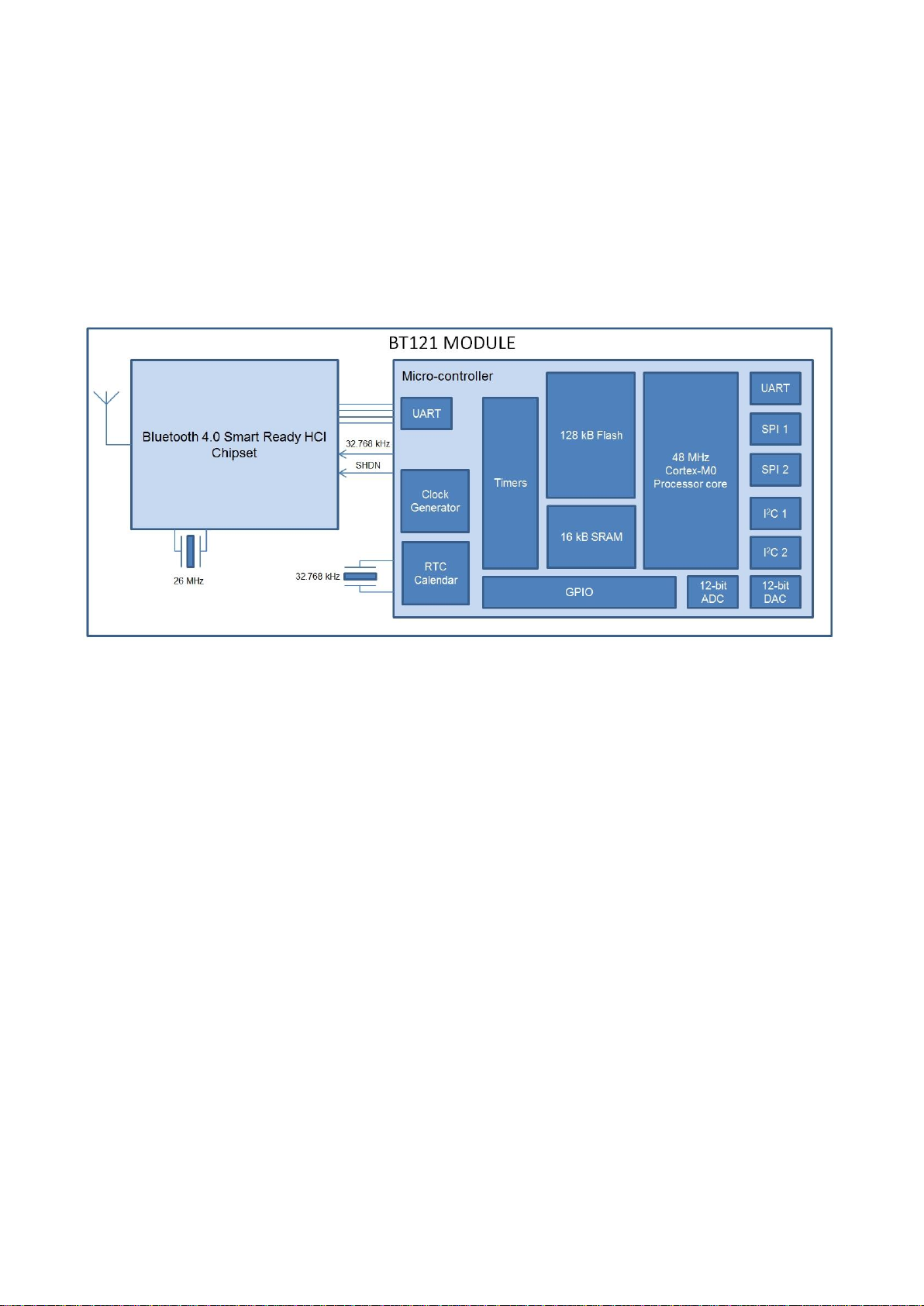
1.3 Block diagram
The block diagram for Bluegiga Bluetooth Smart Ready module BT121 is shown in below.
Figure 1 BT121 Bluetooth Smart Ready module block diagram
Bluegiga – A Silicon Labs Company 7

Design guidelines
Certain hardware related design guidelines should always be followed when developing applications based on
the BT121 module.
2.1 PCB layout recommendations
All ground pads should be connected to a ground plane.
The antenna layout should follow the example shown in Figure 2 below and avoid the designs shown
as crossed over.
BT121 requires minimal free space around the module and only the white area marked in the PCB
picture series presented in Figure 2 below needs to be free of copper and components.
Figure 2 PCB layout recommendations for BT121 application boards
2.2 Power supply recommendations
The regulator used must be capable of supplying a peak current of 150 mA and the regulator must be of a
type stable with ceramic capacitors.
2.3 Software application related options
BT121 can be used either as a stand-alone solution by using the Bluegiga BGScript™ scripting language or
alternatively if the application software size or other factors require together with an external host processor by
using Bluegiga BGAPI™ commands. The decision on which approach to use is most often dictated by the
limits set by the internal memory of the BT121 module.
2.4 Firmware updating related recommendations
To enable firmware updating an external UART interface connection as shown in Figure 3 on the next page is
mandatory. BT121 firmware can be updated through the UART interface by holding the host MCU in reset
state which typically will free the UART lines to be used by the update interface.
Bluegiga – A Silicon Labs Company 8
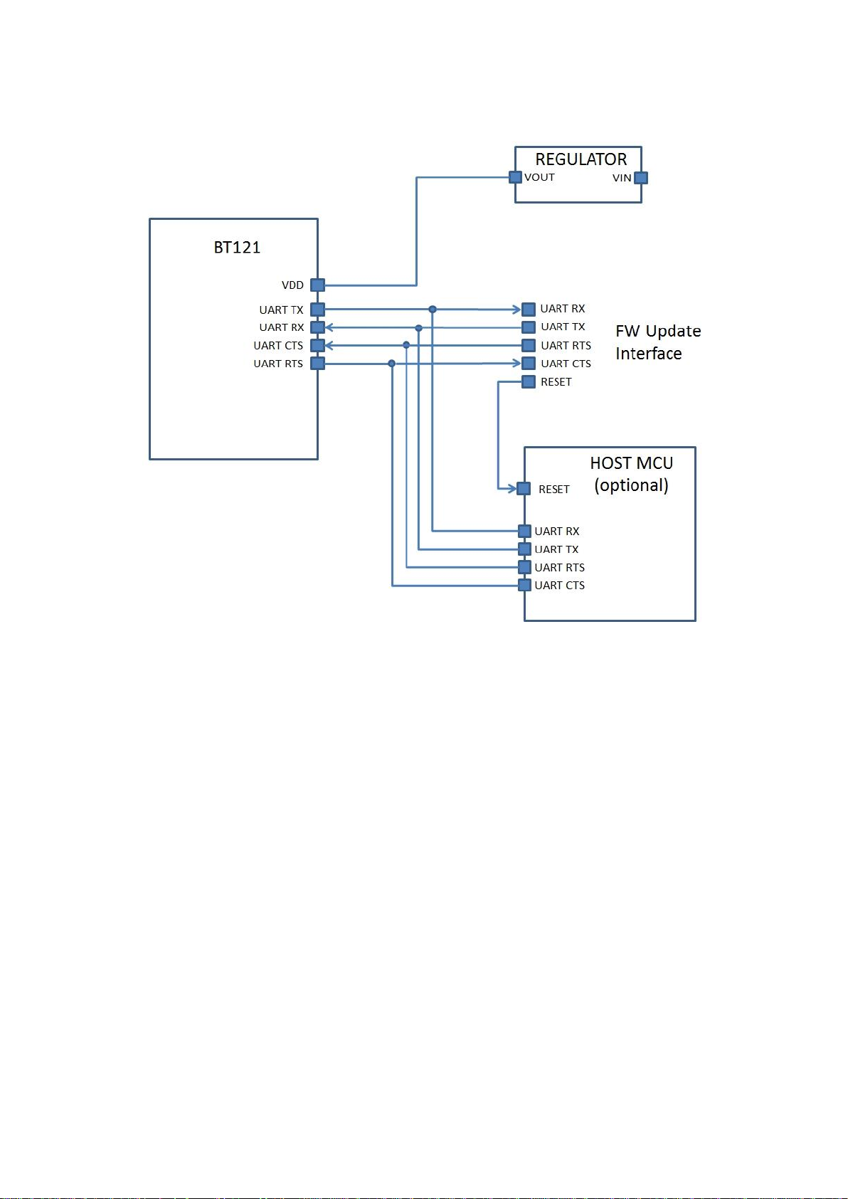
Figure 3 BT121 firmware update via UART connection example
Bluegiga – A Silicon Labs Company 9
Pin / Pad
Function
Description
30,34
VDD
Module power supply input pins.
1, 2, 3, 13, 21,
31, 32, 33, 41
GND
Ground pin. These are all connected together internally but they should all be individually
connected directly to a solid ground plane with vias in close proximity to the pins. This requirement
concerns especially the antenna connections.
22,40
RESET
Module reset signal pins. Pulling RESET low will reset the internal processor of the module. These
connections have an internal pull-up and can be left floating if not needed.
23,35
BOOT0
Boot mode pin of the microcontroller internal boot loader. This connection has an internal pull-down
and should be left floating or pulled low in normal operation.
If the Bluegiga DFU is overwritten or disabled, pulling BOOT0 high at reset will allow DFU to be
rewritten through the UART (serial port interface).
Pin-out description
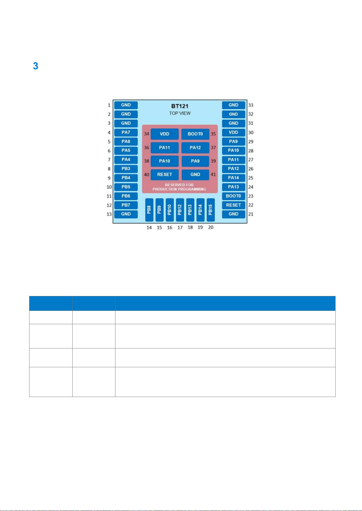
This section contains a description of the BT121 pin-out. Each pin may have one or more functions which are
all listed in tables. The pin-out is shown in Figure 4 below.
Figure 4 BT121 pin-out (top view)
3.1 Power, ground, reset, RF and boot loader pins
Power supply, ground, reset signal, RF antenna input/output and boot loader related pins are listed in Table 1
below.
Table 1 Power, ground, reset, RF and boot loader pins
Bluegiga – A Silicon Labs Company 10
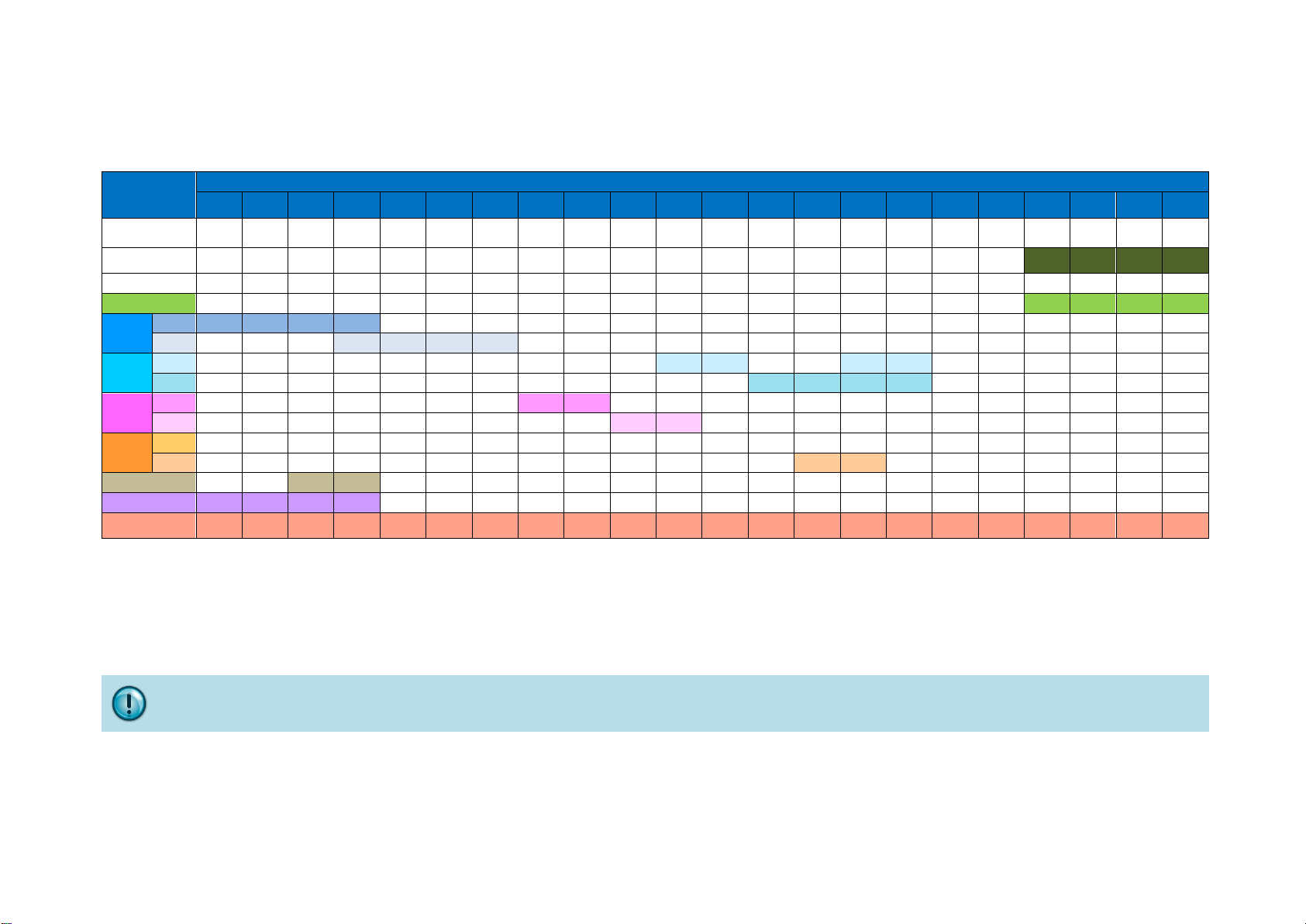
PERIPHERAL
FUNCTION
GPIO NAME
PA7
PA6
PA5
PA4
PB3
PB4
PB5
PB6
PB7
PB8
PB9
PB10
PB12
PB13
PB14
PB15
PA13
PA14
RTS
PA12
CTS
PA11
RX
PA10
TX
PA9
PIN NUMBER
4 5 6 7 8 9 10
11
12
14
15
16
17
18
19
20
24
25
26
37
27
36
28
38
29
39
DEFAULT
FUNCTION **
dc
dc
dc
dc
dc
dc
dc
dc
dc
dc
dc
dc
dc
dc
dc
dc
dc
dc
RTS
CTS
RX
TX
5V TOLERANT
N N N N Y Y Y Y Y Y Y Y Y Y Y Y Y Y Y Y Y
Y
UART ***
RTS
CTS
RX
TX
SPI 1
Alt.1
MOSI
MISO
SCK
NSS*
Alt.2 NSS*
SCK
MISO
MOSI
SPI 2
Alt.1
NSS*
SCK
MISO
MOSI
Alt.2
NSS*
SCK
MISO
MOSI
I2C 1
Alt.1 SCL
SDA Alt.2 SCL
SDA
I2C 2
Alt.1
Alt.2 SCL
SDA
DAC output
AO2
AO1
ADC input
AIN7
AIN6
AIN5
AIN4
Interrupt
channel
7 6 5 4 3 4 5 6 7 8 9
10
12
13
14
15
13
14
12
11
10
9
I2C 2 cannot be used in Alt. 2 configuration
3.2 GPIO pins
General purpose I/O pins and their functions are listed below.
* NSS signal is optional, see SPI description (Section 5.4 ) GPIO pins 36, 37, 38 and 39
** Default pin functions on production firmware / dc = disconnected, no need to pull up or down Reserved for production testing
*** UART can be used as a BGAPI™ host interface and DFU firmware updates Must be left unconnected
If the pins are set as GPIO rather than UART signals the DFU cannot work, see UART (Section 5.2 ) and recovery mode (Section 4.4 )
Bluegiga – A Silicon Labs Company 11
Table 2 General purpose I/O pins and their functions

Power control
4.1 Power supply requirements
BT121 is powered by a single power supply input (VDD). Nominal input voltage is 3.3 VDC and input voltage
range 2.2 V to 3.6 V. If the module’s internal ADC and/or DAC functions are used minimum allowed power
supply voltage is 2.4V.
The VDD supply should be capable of supplying a peak current of at least 150 mA even though the average
current consumption of BT121 will be much less than that. External high frequency bypass capacitors are not
needed because the module contains the necessary power supply filtering capacitors.
Careful design of the layout and proper component selection are necessary to prevent switching noise from
appearing on the supply line. Such disturbances can be caused by on-board charge pump converters (e.g.
RS232 level shifters). Charge pump based converters tend to have strong switching spikes which are difficult
to filter out and may degrade RF performance. A ferrite chip can be added in series with the supply line close
to the module supply pin to reduce RF interference through the supply line.
There is a total of about 1.5 µF of ceramic capacitors on the VDD line inside the module. When using low drop
linear regulators to generate a regulated supply voltage for the VDD line, the stability of the regulator with the
low ESR provided by these capacitors should be checked. Many linear regulators and some switched mode
ones too are not stable when used with ceramic output capacitors. The regulator datasheets usually have
recommendations for output capacitor ESR range or they contain a stability curve to help select components
properly. A regulator designated as “stable with ceramic capacitors” is recommended.
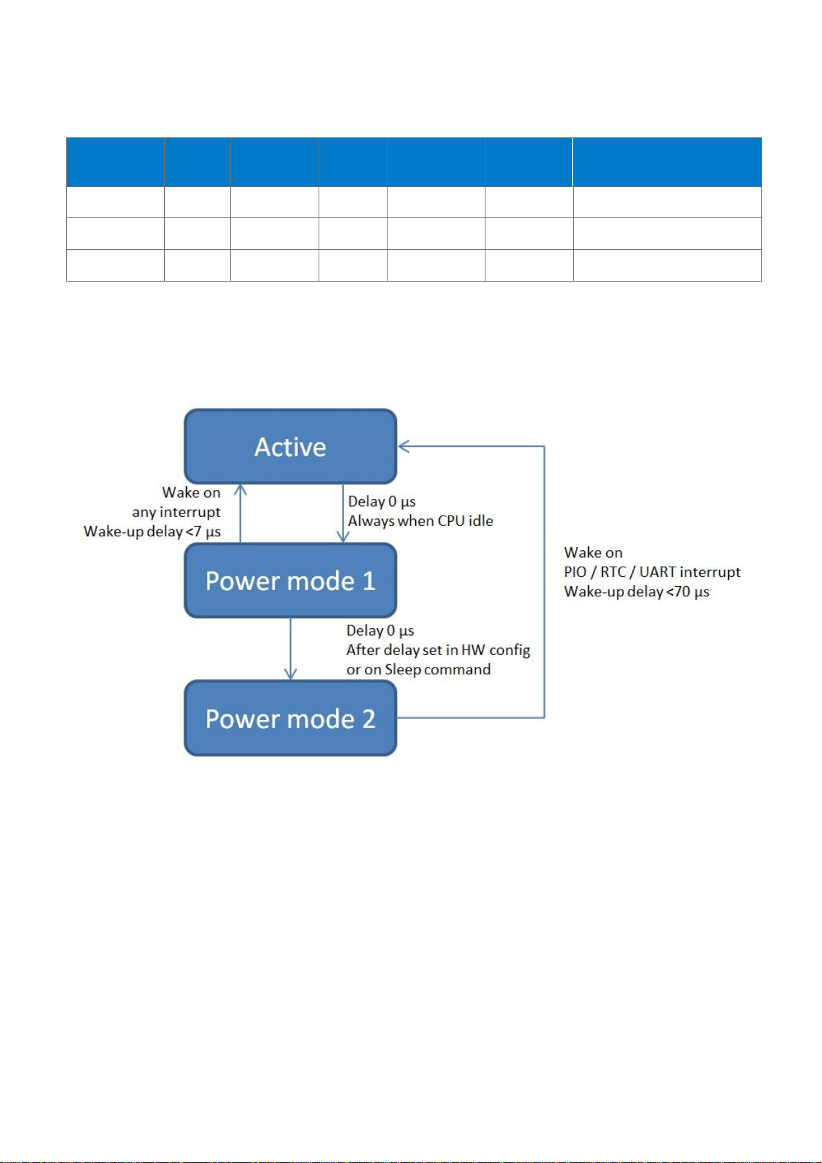
4.2 Power saving functionality
BT121 contains two configurable power saving modes. The internal RTC (Real Time Clock) is usually kept
always running to avoid the long wake-up time associated with the internal 32 kHz crystal oscillator. The RTC
is always available to wake up the module.
4.2.1 Power mode 1
Power mode 1 is a shallow sleep state with all clocks and peripherals running but with the processor core
stopped. It is used automatically and has no impact on module performance and does not require special
considerations in user applications. See Table 3 on next page.
4.2.2 Power mode 2
Power mode 2 is a deep sleep state, in which most peripheral devices and system clocks are powered down.
The UART interfaces cannot operate without clocks, and instant communications with the host are not
possible. A separate wake-up command on the host UART or a PIO interrupt can be used to wake up the
module, or an RTC event. The radio can also cause a wake-up event. There is a short wake-up delay due to
the time required for the internal clocks to stabilize and because of this the module processor is not instantly
ready to receive data. See Table 3 on next page.
Bluegiga – A Silicon Labs Company 12
Power mode
CPU
clocks
CPU
core
Radio
Wakeup
delay
UART
Current
consumption *
Active
ON
Running
On - Active
10 - 20 mA
Power mode 1
ON
Stopped
On
< 7μs
Active
4 - 10 mA
Power mode 2
OFF
Powered off
On
< 70 μs
Off
50 - 100 μA
Table 3 Power modes with corresponding wakeup delays and current consumption
* Current consumption with radio inactive
The logic flow of the power saving modes in relation to each other is shown in Figure 5 below. It is to be noted
that the processor will not lose RAM contents regardless of the power mode used.
4.3 Reset
BT121 can be reset by several methods: by pulling the RESET pin low, by the internal system power-up reset
functionality or by the internal watchdog timer. The RESET pin is internally connected to a pull-up resistor with
a resistance of approximately 40 kohm. The RESET pin should be connected to a push-button, header or test
point to enable the use of the system recovery mode.
Bluegiga – A Silicon Labs Company 13
Figure 5 Power modes in relation to each other and to active mode

4.4 Recovery mode
Pulling the BOOT0 pin high at reset sets the BT121 module’s internal microcontroller into a recovery mode,
which allows the Bluegiga DFU to be rewritten to the module using the DumoGUI software. The BOOT0 pin
should be connected to a header or test point to enable DFU recovery. The pin is internally connected to a 10
kohm pull-down resistor.
4.5 Clock signals
BT121 generates all the required clock signals internally. The clocks used by the internal microcontroller and
external peripherals are synchronized to an internal 32.768 kHz crystal connected to the internal RTC. The
micro power RTC is always kept running when the module is supplied with power. It will take approximately
two seconds for the RTC oscillator to stabilize after power is connected. To avoid this delay it is recommended
that the power supply feed to the BT121 is not switched off but instead the module can be set into the lowest
power mode providing the smallest current consumption.
Bluegiga – A Silicon Labs Company 14
 Loading...