

Silicon Laboratories Finland BGM13P Installation Instructions
BGM13P Blue Gecko Bluetooth ® Module
Data Sheet
The BGM13P Blue Gecko Bluetooth ® Module (BGM13P) is a small form factor, certified
module, enabling rapid development of Bluetooth Low Energy solutions.
Based on the Silicon Labs EFR32BG13 Blue Gecko SoC, the BGM13P combines an energy- efficient, Bluetooth wireless SoC with a proven RF/antenna design and Bluetooth 5
compliant Bluetooth stack. This integration accelerates time-to-market and saves months
of engineering effort and development costs. In addition, common software and development tools enable seamless migration between modules, SIPs and SoC based designs.
BGM13P modules can be used in a wide variety of applications:
• IoT end devices and gateways
• Health, sports and wellness devices
• Industrial, home and building automation
• Smart phone, tablet and PC accessories
• Beacons
Core / Memory
TM
ARM Cortex
with DSP extensions, FPU and MPU
M4 processor
ETM Debug Interface RAM Memory
Flash Program
Memory
LDMA
Controller
Crystals
38.4 MHz
32.768 kHz
Clock Management
H-F Crystal
Oscillator
Auxiliary H-F RC
Oscillator
L-F Crystal
Oscillator
H-F
RC Oscillator
L-F
RC Oscillator
Ultra L-F RC
Oscillator
KEY FEATURES
• Bluetooth 5 low energy compliant
• Integrated antenna or U.FL connector
• TX power up to 8 dBm
• RX sensitivity: -95 dBm
• Range: up to 200 meters
• 32-bit ARM® Cortex®-M4 core at 38.4
MHz
• Flash memory: 512 kB
• RAM: 64 kB
• Autonomous Hardware Crypto Accelerator
and Random Number Generator
• Integrated DC-DC Converter
• Onboard Bluetooth stack
Energy Management
Voltage
Regulator
DC-DC
Converter
Brown-Out
Detector
Voltage Monitor
Power-On Reset
Other
CRYPTO
CRC
True Random
Number Generator
SMU
32-bit bus
Peripheral Reflex System
Antenna
Chip Antenna
or
U.FL Connector
Matching
Lowest power mode with peripheral operational:
LNA
BALUN
RF Frontend
PA
Radio Transceiver
PGA
I
Frequency
Q
Synthesizer
DEMOD
IFADC
AGC
MOD
FRC
CRC
BUFC
RAC
Serial
Interfaces
USART
Low Energy
TM
UART
2
I
C
I/O Ports Analog I/F
External
Interrupts
General
Purpose I/O
Pin Reset
Pin Wakeup
EM3—StopEM2—Deep SleepEM1—Sleep EM4—Hibernate EM4—ShutoffEM0—Active
Timers and Triggers
Timer/Counter
Low Energy
Timer
Pulse Counter Watchdog Timer
Real Time
Counter and
Calendar
Protocol Timer
Low Energy
Sensor Interface
Cryotimer
ADC
Analog
Comparator
IDAC
Capacitive
Touch
VDAC
Op-Amp
silabs.com | Building a more connected world. Rev. 1.0

1. Feature List
The BGM13P highlighted features are listed below.
• Low Power Wireless System-on-Chip.
•
High Performance 32-bit 38.4 MHz ARM Cortex®-M4 with
DSP instruction and floating-point unit for efficient signal
processing
• Embedded Trace Macrocell (ETM) for advanced debugging
• 512 kB flash program memory
• 64 kB RAM data memory
• 2.4 GHz radio operation
• TX power up to 8 dBm
• Low Energy Consumption
• 9.9 mA RX current
• 8.5 mA TX current at 0 dBm output power
• 87 μA/MHz in Active Mode (EM0)
• 1.4 μA EM2 DeepSleep current (full RAM retention and
RTCC running from LFXO)
• 1.14 μA EM3 Stop current (State/RAM retention)
• Wake on Radio with signal strength detection, preamble
pattern detection, frame detection and timeout
• High Receiver Performance
• -103.2 dBm sensitivity at 125 kbit/s GFSK
• -95 dBm sensitivity at 1 Mbit/s GFSK
• -91.2 dBm sensitivity at 2 Mbit/s GFSK
• Supported Protocols
• Bluetooth Low Energy (Bluetooth 5)
• Support for Internet Security
• General Purpose CRC
• True Random Number Generator (TRNG)
• 2 × Hardware Cryptographic Accelerators (CRYPTO) for
AES 128/256, SHA-1, SHA-2 (SHA-224 and SHA-256) and
ECC
• Regulatory Certifications
• FCC
• CE
• IC / ISEDC
• MIC / Telec
BGM13P Blue Gecko Bluetooth ® Module Data Sheet
Feature List
• Wide selection of MCU peripherals
• 12-bit 1 Msps SAR Analog to Digital Converter (ADC)
• 2 × Analog Comparator (ACMP)
• 2 × Digital to Analog Converter (VDAC)
• 3 × Operational Amplifier (Opamp)
• Digital to Analog Current Converter (IDAC)
• Low-Energy Sensor Interface (LESENSE)
• Multi-channel Capacitive Sense Interface (CSEN)
• 25 pins connected to analog channels (APORT) shared between analog peripherals
• 25 General Purpose I/O pins with output state retention and
asynchronous interrupts
• 8 Channel DMA Controller
• 12 Channel Peripheral Reflex System (PRS)
• 2 × 16-bit Timer/Counter
• 3 or 4 Compare/Capture/PWM channels
• 1 × 32-bit Timer/Counter
• 3 Compare/Capture/PWM channels
• 32-bit Real Time Counter and Calendar
• 16-bit Low Energy Timer for waveform generation
• 32-bit Ultra Low Energy Timer/Counter for periodic wake-up
from any Energy Mode
• 16-bit Pulse Counter with asynchronous operation
• 2 × Watchdog Timer
• 3 × Universal Synchronous/Asynchronous Receiver/Transmitter (UART/SPI/SmartCard (ISO 7816)/IrDA/I2S)
•
Low Energy UART (LEUART™)
•
2 × I2C interface with SMBus support and address recognition in EM3 Stop
• Wide Operating Range
• 1.8 V to 3.8 V single power supply
• Integrated DC-DC
• -40 °C to +85 °C
• Dimensions
• 12.9 × 15.0 × 2.2 mm (W × L × H)
silabs.com | Building a more connected world. Rev. 1.0 | 2

2. Ordering Information
BGM13P Blue Gecko Bluetooth ® Module Data Sheet
Ordering Information
Table 2.1. Ordering Information
Frequency Band
Ordering Code Protocol Stack
BGM13P22F512GA-V2R Bluetooth Low
Energy
BGM13P22F512GA-V2 Bluetooth Low
Energy
BGM13P22F512GE-V2R Bluetooth Low
Energy
BGM13P22F512GE-V2 Bluetooth Low
Energy
Devices ship with the Gecko UART DFU bootloader 1.4.1 + NCP application from Bluetooth SDK 2.7.0.0. The firmware settings conform to the diagram shown in 5.1 Network Co-Processor (NCP) Application with UART Host.
@ Max TX Power Antenna
2.4 GHz @ 8 dBm Built-in 512 64 25 Reel
2.4 GHz @ 8 dBm Built-in 512 64 25 Tray
2.4 GHz @ 8 dBm U.FL 512 64 25 Reel
2.4 GHz @ 8 dBm U.FL 512 64 25 Tray
Flash
(kB)
RAM
(kB) GPIO Packaging
silabs.com | Building a more connected world. Rev. 1.0 | 3

Table of Contents
1. Feature List ................................2
2. Ordering Information ............................3
3. System Overview ..............................7
3.1 Introduction...............................7
3.2 Radio.................................7
3.2.1 Antenna Interface ..........................7
3.2.2 RFSENSE .............................8
3.2.3 Packet and State Trace ........................8
3.2.4 Random Number Generator .......................8
3.3 Power ................................9
3.3.1 Energy Management Unit (EMU) .....................9
3.3.2 DC-DC Converter ..........................9
3.3.3 Power Domains ...........................10
3.4 General Purpose Input/Output (GPIO)......................10
3.5 Clocking ................................10
3.5.1 Clock Management Unit (CMU) ......................10
3.5.2 Internal Oscillators and Crystals......................10
3.6 Counters/Timers and PWM .........................11
3.6.1 Timer/Counter (TIMER) ........................11
3.6.2 Wide Timer/Counter (WTIMER) ......................11
3.6.3 Real Time Counter and Calendar (RTCC) ..................11
3.6.4 Low Energy Timer (LETIMER) ......................11
3.6.5 Ultra Low Power Wake-up Timer (CRYOTIMER) ................11
3.6.6 Pulse Counter (PCNT) .........................11
3.6.7 Watchdog Timer (WDOG) ........................11
3.7 Communications and Other Digital Peripherals ...................12
3.7.1 Universal Synchronous/Asynchronous Receiver/Transmitter (USART) .........12
3.7.2 Low Energy Universal Asynchronous Receiver/Transmitter (LEUART) .........12
3.7.3 Inter-Integrated Circuit Interface (I2C) ....................12
3.7.4 Peripheral Reflex System (PRS) .....................12
3.7.5 Low Energy Sensor Interface (LESENSE) ..................12
3.8 Security Features.............................12
3.8.1 GPCRC (General Purpose Cyclic Redundancy Check) ..............12
3.8.2 Crypto Accelerator (CRYPTO) ......................13
3.8.3 True Random Number Generator (TRNG) ..................13
3.8.4 Security Management Unit (SMU) .....................13
3.9 Analog ................................13
3.9.1 Analog Port (APORT) .........................13
3.9.2 Analog Comparator (ACMP) .......................13
3.9.3 Analog to Digital Converter (ADC) .....................13
3.9.4 Capacitive Sense (CSEN) ........................13
3.9.5 Digital to Analog Current Converter (IDAC) ..................14
silabs.com
| Building a more connected world. Rev. 1.0 | 4

3.9.6 Digital to Analog Converter (VDAC) ....................14
3.9.7 Operational Amplifiers .........................14
3.10 Reset Management Unit (RMU) .......................14
3.11 Core and Memory ............................14
3.11.1 Processor Core ...........................14
3.11.2 Memory System Controller (MSC) ....................14
3.11.3 Linked Direct Memory Access Controller (LDMA) ...............14
3.12 Memory Map ..............................15
3.13 Configuration Summary ..........................16
4. Electrical Specifications ..........................17
4.1 Electrical Characteristics ..........................17
4.1.1 Absolute Maximum Ratings .......................18
4.1.2 Operating Conditions .........................19
4.1.3 DC-DC Converter ..........................20
4.1.4 Current Consumption .........................21
4.1.5 Wake Up Times ...........................24
4.1.6 Brown Out Detector (BOD) .......................24
4.1.7 Frequency Synthesizer .........................25
4.1.8 2.4 GHz RF Transceiver Characteristics ...................26
4.1.9 Oscillators .............................29
4.1.10 Flash Memory Characteristics ......................31
4.1.11 General-Purpose I/O (GPIO) ......................32
4.1.12 Voltage Monitor (VMON) ........................34
4.1.13 Analog to Digital Converter (ADC) ....................35
4.1.14 Current Digital to Analog Converter (IDAC) .................37
4.1.15 Analog Comparator (ACMP) ......................39
4.1.16 I2C ...............................41
4.1.17 USART SPI ............................44
5. Typical Connection Diagrams ........................46
5.1 Network Co-Processor (NCP) Application with UART Host ...............46
5.2 SoC Application .............................46
6. Layout Guidelines ............................47
6.1 Module Placement and Application PCB Layout Guidelines ..............47
6.2 Effect of Plastic and Metal Materials ......................48
6.3 Locating the Module Close to Human Body ....................48
6.4 2D Radiation Pattern Plots .........................49
7. Hardware Design Guidelines ........................51
7.1 Power Supply Requirements .........................51
7.2 Reset Functions .............................51
7.3 Debug and Firmware Updates ........................51
7.3.1 Programming and Debug Connections ...................51
7.3.2 Packet Trace Interface (PTI) .......................51
silabs.com
| Building a more connected world. Rev. 1.0 | 5

8. Pin Definitions ..............................52
8.1 BGM13P Device Pinout ..........................52
8.2 GPIO Functionality Table ..........................54
8.3 Alternate Functionality Overview .......................64
8.4 Analog Port (APORT) Client Maps .......................74
9. Package Specifications ..........................83
9.1 BGM13P Dimensions ...........................83
9.2 BGM13P Module Footprint .........................83
9.3 BGM13P Recommended PCB Land Pattern ...................84
10. Tape and Reel Specifications ........................85
10.1 Tape and Reel Specification ........................85
10.2 Reel Material and Dimensions ........................85
10.3 Module Orientation and Tape Feed ......................86
10.4 Cover Tape Information ..........................86
11. Soldering Recommendations ........................87
11.1 Soldering Recommendations ........................87
12. Certifications ..............................88
12.1 Qualified Antenna Types ..........................88
12.2 Bluetooth ...............................88
12.3 CE .................................88
12.4 FCC.................................89
12.5 ISED Canada .............................90
12.6 Japan ................................92
13. Revision History............................. 93
silabs.com
| Building a more connected world. Rev. 1.0 | 6

BGM13P Blue Gecko
Bluetooth ® Module Data Sheet
System Overview
3. System Overview
3.1 Introduction
The BGM13P product family combines an energy-friendly MCU with a highly integrated radio transceiver and a high performance, ultra
robust antenna. The devices are well suited for any battery operated application, as well as other system where ultra-small size, reliable
high performance RF, low-power consumption and easy application development are key requirements. This section gives a short introduction to the full radio and MCU system.
A detailed block diagram of the BGM13P Bluetooth Smart module is shown in the figure below.
RESETn
Debug Signals
(shared w/GPIO)
IOVDD
1V8
VBAT
Antenna
Chip
Antenna
or
U.FL
Connector
Matching
Serial Wire
and ETM
Debug /
Programming
Energy Management
PAVDD / RFVDD / DVDD
bypass
DC-DC
Converter
VREGVDD / AVDD
Internal Crystals
32.768 kHz
38.4 MHz Crystal
BALUN
Crystal
RF Frontend
LNA
PA
Reset
Management
Unit
Brown Out /
Power-On
Reset
Voltage
Monitor
Voltage
Regulator
Radio Transciever
PGA
I
Frequency
Q
Synthesizer
ARM Cortex-M4 Core
512 KB ISP Flash
Program Memory
Memory Protection Unit
Floating Point Unit
Watchdog
Clock Management
ULFRCO
AUXHFRCO
DEMOD
IFADC
AGC
MOD
64 KB RAM
DMA Controller
Timer
LFRCO
LFXO
HFRCO
HFXO
FRC
CRC
BUFC
RAC
Port I/O Configuration
IOVDD
Digital Peripherals
LETIMER
TIMER
CRYOTIMER
PCNT
RTC / RTCC
USART
LEUART
I2C
CRYPTO
A
A
H
P
B
B
CRC
LESENSE
Port
Mapper
Port A
Drivers
Port B
Drivers
Port C
Drivers
Port D
Drivers
Port F
Drivers
PAn
PBn
PCn
PDn
PFn
Analog Peripherals
IDAC
-
Mux & FB
Input Mux
+
-
+
Op-Amp
VDD
Temp
Sense
APORT
VDAC
Internal
Reference
12-bit ADC
Capacitive
Touch
Analog Comparator
Figure 3.1. BGM13P Block Diagram
3.2 Radio
The BGM13P features a radio transceiver supporting Bluetooth® low energy protocol.
3.2.1 Antenna Interface
BGM13P module family includes options for either a high-performance, integrated chip antenna (BGM13PxxFxxxGA), or external antenna via a U.FL connector (BGM13PxxFxxxGE). The table below includes performance specifications for the integrated chip antenna.
silabs.com | Building a more connected world. Rev. 1.0 | 7

BGM13P Blue Gecko Bluetooth ® Module Data Sheet
System Overview
Table 3.1. Antenna Efficiency and Peak Gain
Parameter With optimal layout Note
Efficiency -2 to -4 dB Antenna efficiency, gain and radiation pattern are highly depend-
Peak gain 1 dBi
3.2.2 RFSENSE
The RFSENSE module generates a system wakeup interrupt upon detection of wideband RF energy at the antenna interface, providing
true RF wakeup capabilities from low energy modes including EM2, EM3 and EM4.
RFSENSE triggers on a relatively strong RF signal and is available in the lowest energy modes, allowing exceptionally low energy consumption. RFSENSE does not demodulate or otherwise qualify the received signal, but software may respond to the wakeup event by
enabling normal RF reception.
Various strategies for optimizing power consumption and system response time in presence of false alarms may be employed using
available timer peripherals.
ent on the application PCB layout and mechanical design. Refer
to 6. Layout Guidelines for PCB layout and antenna integration
guidelines for optimal performance. Typical efficiency gain is expected to be from -3.5 to -5.5 dB.
3.2.3 Packet and State Trace
The BGM13P Frame Controller has a packet and state trace unit that provides valuable information during the development phase. It
features:
• Non-intrusive trace of transmit data, receive data and state information
• Data observability on a single-pin UART data output, or on a two-pin SPI data output
• Configurable data output bitrate / baudrate
• Multiplexed transmitted data, received data and state / meta information in a single serial data stream
3.2.4 Random Number Generator
The Frame Controller (FRC) implements a random number generator that uses entropy gathered from noise in the RF receive chain.
The data is suitable for use in cryptographic applications.
Output from the random number generator can be used either directly or as a seed or entropy source for software-based random number generator algorithms such as Fortuna.
silabs.com | Building a more connected world. Rev. 1.0 | 8
BGM13P Blue Gecko Bluetooth ® Module Data Sheet
System Overview
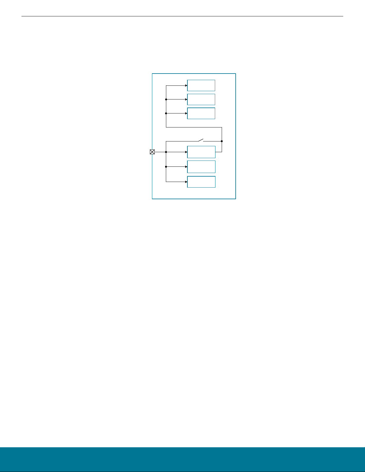
3.3 Power
The BGM13P has an Energy Management Unit (EMU) and efficient integrated regulators to generate internal supply voltages. Only a
single external supply voltage is required, from which all internal voltages are created. An integrated DC-DC buck regulator is utilized to
further reduce the current consumption. Figure 3.2 Power Supply Configuration for +8 dBm Devices on page 9 shows how the external and internal supplies of the module are connected.
VDD
DVDD
PAVDD
RFVDD
VREGVDD
AVDD
IOVDD
Digital
RF PA
RF
DC-DC
Analog
I/O Interfaces
Figure 3.2. Power Supply Configuration for +8 dBm Devices
3.3.1 Energy Management Unit (EMU)
The Energy Management Unit manages transitions of energy modes in the device. Each energy mode defines which peripherals and
features are available and the amount of current the device consumes. The EMU can also be used to turn off the power to unused RAM
blocks, and it contains control registers for the dc-dc regulator and the Voltage Monitor (VMON). The VMON is used to monitor multiple
supply voltages. It has multiple channels which can be programmed individually by the user to determine if a sensed supply has fallen
below a chosen threshold.
3.3.2 DC-DC Converter
The DC-DC buck converter covers a wide range of load currents and provides up to 90% efficiency in energy modes EM0, EM1, EM2
and EM3. Patented RF noise mitigation allows operation of the DC-DC converter without degrading sensitivity of radio components.
Protection features include programmable current limiting, short-circuit protection, and dead-time protection. The DC-DC converter may
also enter bypass mode when the input voltage is too low for efficient operation. In bypass mode, the DC-DC input supply is internally
connected directly to its output through a low resistance switch. Bypass mode also supports in-rush current limiting to prevent input
supply voltage droops due to excessive output current transients.
silabs.com | Building a more connected world. Rev. 1.0 | 9

BGM13P Blue Gecko
Bluetooth ® Module Data Sheet
System Overview
3.3.3 Power Domains
The BGM13P has two peripheral power domains for operation in EM2 and lower. If all of the peripherals in a peripheral power domain
are configured as unused, the power domain for that group will be powered off in the low-power mode, reducing the overall current
consumption of the device.
Table 3.2. Peripheral Power Subdomains
Peripheral Power Domain 1 Peripheral Power Domain 2
ACMP0 ACMP1
PCNT0 CSEN
ADC0 VDAC0
LETIMER0 LEUART0
LESENSE I2C0
APORT I2C1
- IDAC
3.4 General Purpose Input/Output (GPIO)
BGM13P has up to 25 General Purpose Input/Output pins. Each GPIO pin can be individually configured as either an output or input.
More advanced configurations including open-drain, open-source, and glitch-filtering can be configured for each individual GPIO pin.
The GPIO pins can be overridden by peripheral connections, like SPI communication. Each peripheral connection can be routed to several GPIO pins on the device. The input value of a GPIO pin can be routed through the Peripheral Reflex System to other peripherals.
The GPIO subsystem supports asynchronous external pin interrupts.
3.5 Clocking
3.5.1 Clock Management Unit (CMU)
The Clock Management Unit controls oscillators and clocks in the BGM13P. Individual enabling and disabling of clocks to all peripheral
modules is performed by the CMU. The CMU also controls enabling and configuration of the oscillators. A high degree of flexibility allows software to optimize energy consumption in any specific application by minimizing power dissipation in unused peripherals and
oscillators.
3.5.2 Internal Oscillators and Crystals
The BGM13P fully integrates several oscillator sources and two crystals.
• The high-frequency crystal oscillator (HFXO) and integrated 38.4 MHz crystal provide a precise timing reference for the MCU and
radio.
• The low-frequency crystal oscillator (LFXO) and integrated 32.768 kHz crystal provide an accurate timing reference for low energy
modes and the real-time-clock circuits.
• An integrated high frequency RC oscillator (HFRCO) is available for the MCU system, when crystal accuracy is not required. The
HFRCO employs fast startup at minimal energy consumption combined with a wide frequency range.
• An integrated auxilliary high frequency RC oscillator (AUXHFRCO) is available for timing the general-purpose ADC and the Serial
Wire Viewer port with a wide frequency range.
• An integrated low frequency 32.768 kHz RC oscillator (LFRCO) for low power operation where high accuracy is not required.
• An integrated ultra-low frequency 1 kHz RC oscillator (ULFRCO) is available to provide a timing reference at the lowest energy consumption in low energy modes.
silabs.com | Building a more connected world. Rev. 1.0 | 10

BGM13P Blue Gecko
Bluetooth ® Module Data Sheet
System Overview
3.6 Counters/Timers and PWM
3.6.1 Timer/Counter (TIMER)
TIMER peripherals keep track of timing, count events, generate PWM outputs and trigger timed actions in other peripherals through the
PRS system. The core of each TIMER is a 16-bit counter with up to 4 compare/capture channels. Each channel is configurable in one
of three modes. In capture mode, the counter state is stored in a buffer at a selected input event. In compare mode, the channel output
reflects the comparison of the counter to a programmed threshold value. In PWM mode, the TIMER supports generation of pulse-width
modulation (PWM) outputs of arbitrary waveforms defined by the sequence of values written to the compare registers, with optional
dead-time insertion available in timer unit TIMER_0 only.
3.6.2 Wide Timer/Counter (WTIMER)
WTIMER peripherals function just as TIMER peripherals, but are 32 bits wide. They keep track of timing, count events, generate PWM
outputs and trigger timed actions in other peripherals through the PRS system. The core of each WTIMER is a 32-bit counter with up to
4 compare/capture channels. Each channel is configurable in one of three modes. In capture mode, the counter state is stored in a
buffer at a selected input event. In compare mode, the channel output reflects the comparison of the counter to a programmed threshold value. In PWM mode, the WTIMER supports generation of pulse-width modulation (PWM) outputs of arbitrary waveforms defined by
the sequence of values written to the compare registers, with optional dead-time insertion available in timer unit WTIMER_0 only.
3.6.3 Real Time Counter and Calendar (RTCC)
The Real Time Counter and Calendar (RTCC) is a 32-bit counter providing timekeeping in all energy modes. The RTCC includes a
Binary Coded Decimal (BCD) calendar mode for easy time and date keeping. The RTCC can be clocked by any of the on-board oscillators with the exception of the AUXHFRCO, and it is capable of providing system wake-up at user defined instances. When receiving
frames, the RTCC value can be used for timestamping. The RTCC includes 128 bytes of general purpose data retention, allowing easy
and convenient data storage in all energy modes down to EM4H.
A secondary RTC is used by the RF protocol stack for event scheduling, leaving the primary RTCC block available exclusively for application software.
3.6.4 Low Energy Timer (LETIMER)
The unique LETIMER is a 16-bit timer that is available in energy mode EM2 Deep Sleep in addition to EM1 Sleep and EM0 Active. This
allows it to be used for timing and output generation when most of the device is powered down, allowing simple tasks to be performed
while the power consumption of the system is kept at an absolute minimum. The LETIMER can be used to output a variety of waveforms with minimal software intervention. The LETIMER is connected to the Real Time Counter and Calendar (RTCC), and can be configured to start counting on compare matches from the RTCC.
3.6.5 Ultra Low Power Wake-up Timer (CRYOTIMER)
The CRYOTIMER is a 32-bit counter that is capable of running in all energy modes. It can be clocked by either the 32.768 kHz crystal
oscillator (LFXO), the 32.768 kHz RC oscillator (LFRCO), or the 1 kHz RC oscillator (ULFRCO). It can provide periodic Wakeup events
and PRS signals which can be used to wake up peripherals from any energy mode. The CRYOTIMER provides a wide range of interrupt periods, facilitating flexible ultra-low energy operation.
3.6.6 Pulse Counter (PCNT)
The Pulse Counter (PCNT) peripheral can be used for counting pulses on a single input or to decode quadrature encoded inputs. The
clock for PCNT is selectable from either an external source on pin PCTNn_S0IN or from an internal timing reference, selectable from
among any of the internal oscillators, except the AUXHFRCO. The module may operate in energy mode EM0 Active, EM1 Sleep, EM2
Deep Sleep, and EM3 Stop.
3.6.7 Watchdog Timer (WDOG)
The watchdog timer can act both as an independent watchdog or as a watchdog synchronous with the CPU clock. It has windowed
monitoring capabilities, and can generate a reset or different interrupts depending on the failure mode of the system. The watchdog can
also monitor autonomous systems driven by PRS.
silabs.com | Building a more connected world. Rev. 1.0 | 11

BGM13P Blue Gecko
Bluetooth ® Module Data Sheet
System Overview
3.7 Communications and Other Digital Peripherals
3.7.1 Universal Synchronous/Asynchronous Receiver/Transmitter (USART)
The Universal Synchronous/Asynchronous Receiver/Transmitter is a flexible serial I/O module. It supports full duplex asynchronous
UART communication with hardware flow control as well as RS-485, SPI, MicroWire and 3-wire. It can also interface with devices supporting:
• ISO7816 SmartCards
• IrDA
•
I2S
3.7.2 Low Energy Universal Asynchronous Receiver/Transmitter (LEUART)
The unique LEUARTTM provides two-way UART communication on a strict power budget. Only a 32.768 kHz clock is needed to allow
UART communication up to 9600 baud. The LEUART includes all necessary hardware to make asynchronous serial communication
possible with a minimum of software intervention and energy consumption.
3.7.3 Inter-Integrated Circuit Interface (I2C)
The I2C module provides an interface between the MCU and a serial I2C bus. It is capable of acting as both a master and a slave and
supports multi-master buses. Standard-mode, fast-mode and fast-mode plus speeds are supported, allowing transmission rates from 10
kbit/s up to 1 Mbit/s. Slave arbitration and timeouts are also available, allowing implementation of an SMBus-compliant system. The
interface provided to software by the I2C module allows precise timing control of the transmission process and highly automated transfers. Automatic recognition of slave addresses is provided in active and low energy modes.
3.7.4 Peripheral Reflex System (PRS)
The Peripheral Reflex System provides a communication network between different peripheral modules without software involvement.
Peripheral modules producing Reflex signals are called producers. The PRS routes Reflex signals from producers to consumer peripherals which in turn perform actions in response. Edge triggers and other functionality such as simple logic operations (AND, OR, NOT)
can be applied by the PRS to the signals. The PRS allows peripheral to act autonomously without waking the MCU core, saving power.
3.7.5 Low Energy Sensor Interface (LESENSE)
The Low Energy Sensor Interface LESENSETM is a highly configurable sensor interface with support for up to 16 individually configurable sensors. By controlling the analog comparators, ADC, and DAC, LESENSE is capable of supporting a wide range of sensors and
measurement schemes, and can for instance measure LC sensors, resistive sensors and capacitive sensors. LESENSE also includes a
programmable finite state machine which enables simple processing of measurement results without CPU intervention. LESENSE is
available in energy mode EM2, in addition to EM0 and EM1, making it ideal for sensor monitoring in applications with a strict energy
budget.
3.8 Security Features
3.8.1 GPCRC (General Purpose Cyclic Redundancy Check)
The GPCRC module implements a Cyclic Redundancy Check (CRC) function. It supports both 32-bit and 16-bit polynomials. The supported 32-bit polynomial is 0x04C11DB7 (IEEE 802.3), while the 16-bit polynomial can be programmed to any value, depending on the
needs of the application.
silabs.com | Building a more connected world. Rev. 1.0 | 12

BGM13P Blue Gecko
Bluetooth ® Module Data Sheet
System Overview
3.8.2 Crypto Accelerator (CRYPTO)
The Crypto Accelerator is a fast and energy-efficient autonomous hardware encryption and decryption accelerator. EFR32 devices support AES encryption and decryption with 128- or 256-bit keys, ECC over both GF(P) and GF(2m), SHA-1 and SHA-2 (SHA-224 and
SHA-256).
Supported block cipher modes of operation for AES include: ECB, CTR, CBC, PCBC, CFB, OFB, GCM, CBC-MAC, GMAC and CCM.
Supported ECC NIST recommended curves include P-192, P-224, P-256, K-163, K-233, B-163 and B-233.
The CRYPTO1 block is tightly linked to the Radio Buffer Controller (BUFC) enabling fast and efficient autonomous cipher operations on
data buffer content. It allows fast processing of GCM (AES), ECC and SHA with little CPU intervention.
CRYPTO also provides trigger signals for DMA read and write operations.
3.8.3 True Random Number Generator (TRNG)
The TRNG module is a non-deterministic random number generator based on a full hardware solution. The TRNG is validated with
NIST800-22 and AIS-31 test suites as well as being suitable for FIPS 140-2 certification (for the purposes of cryptographic key generation).
3.8.4 Security Management Unit (SMU)
The Security Management Unit (SMU) allows software to set up fine-grained security for peripheral access, which is not possible in the
Memory Protection Unit (MPU). Peripherals may be secured by hardware on an individual basis, such that only priveleged accesses to
the peripheral's register interface will be allowed. When an access fault occurs, the SMU reports the specific peripheral involved and
can optionally generate an interrupt.
3.9 Analog
3.9.1 Analog Port (APORT)
The Analog Port (APORT) is an analog interconnect matrix allowing access to many analog modules on a flexible selection of pins.
Each APORT bus consists of analog switches connected to a common wire. Since many clients can operate differentially, buses are
grouped by X/Y pairs.
3.9.2 Analog Comparator (ACMP)
The Analog Comparator is used to compare the voltage of two analog inputs, with a digital output indicating which input voltage is higher. Inputs are selected from among internal references and external pins. The tradeoff between response time and current consumption
is configurable by software. Two 6-bit reference dividers allow for a wide range of internally-programmable reference sources. The
ACMP can also be used to monitor the supply voltage. An interrupt can be generated when the supply falls below or rises above the
programmable threshold.
3.9.3 Analog to Digital Converter (ADC)
The ADC is a Successive Approximation Register (SAR) architecture, with a resolution of up to 12 bits at up to 1 Msps. The output
sample resolution is configurable and additional resolution is possible using integrated hardware for averaging over multiple samples.
The ADC includes integrated voltage references and an integrated temperature sensor. Inputs are selectable from a wide range of
sources, including pins configurable as either single-ended or differential.
3.9.4 Capacitive Sense (CSEN)
The CSEN module is a dedicated Capacitive Sensing block for implementing touch-sensitive user interface elements such a switches
and sliders. The CSEN module uses a charge ramping measurement technique, which provides robust sensing even in adverse conditions including radiated noise and moisture. The module can be configured to take measurements on a single port pin or scan through
multiple pins and store results to memory through DMA. Several channels can also be shorted together to measure the combined capacitance or implement wake-on-touch from very low energy modes. Hardware includes a digital accumulator and an averaging filter,
as well as digital threshold comparators to reduce software overhead.
silabs.com | Building a more connected world. Rev. 1.0 | 13

BGM13P Blue Gecko
Bluetooth ® Module Data Sheet
System Overview
3.9.5 Digital to Analog Current Converter (IDAC)
The Digital to Analog Current Converter can source or sink a configurable constant current. This current can be driven on an output pin
or routed to the selected ADC input pin for capacitive sensing. The full-scale current is programmable between 0.05 µA and 64 µA with
several ranges consisting of various step sizes.
3.9.6 Digital to Analog Converter (VDAC)
The Digital to Analog Converter (VDAC) can convert a digital value to an analog output voltage. The VDAC is a fully differential, 500
ksps, 12-bit converter. The opamps are used in conjunction with the VDAC, to provide output buffering. One opamp is used per singleended channel, or two opamps are used to provide differential outputs. The VDAC may be used for a number of different applications
such as sensor interfaces or sound output. The VDAC can generate high-resolution analog signals while the MCU is operating at low
frequencies and with low total power consumption. Using DMA and a timer, the VDAC can be used to generate waveforms without any
CPU intervention. The VDAC is available in all energy modes down to and including EM3.
3.9.7 Operational Amplifiers
The opamps are low power amplifiers with a high degree of flexibility targeting a wide variety of standard opamp application areas, and
are available down to EM3. With flexible built-in programming for gain and interconnection they can be configured to support multiple
common opamp functions. All pins are also available externally for filter configurations. Each opamp has a rail to rail input and a rail to
rail output. They can be used in conjunction with the VDAC module or in stand-alone configurations. The opamps save energy, PCB
space, and cost as compared with standalone opamps because they are integrated on-chip.
3.10 Reset Management Unit (RMU)
The RMU is responsible for handling reset of the BGM13P. A wide range of reset sources are available, including several power supply
monitors, pin reset, software controlled reset, core lockup reset, and watchdog reset.
3.11 Core and Memory
3.11.1 Processor Core
The ARM Cortex-M processor includes a 32-bit RISC processor integrating the following features and tasks in the system:
• ARM Cortex-M4 RISC processor achieving 1.25 Dhrystone MIPS/MHz
• Memory Protection Unit (MPU) supporting up to 8 memory segments
• Up to 512 kB flash program memory
• Up to 64 kB RAM data memory
• Configuration and event handling of all modules
• 2-pin Serial-Wire debug interface
3.11.2 Memory System Controller (MSC)
The Memory System Controller (MSC) is the program memory unit of the microcontroller. The flash memory is readable and writable
from both the Cortex-M and DMA. The flash memory is divided into two blocks; the main block and the information block. Program code
is normally written to the main block, whereas the information block is available for special user data and flash lock bits. There is also a
read-only page in the information block containing system and device calibration data. Read and write operations are supported in energy modes EM0 Active and EM1 Sleep.
3.11.3 Linked Direct Memory Access Controller (LDMA)
The Linked Direct Memory Access (LDMA) controller allows the system to perform memory operations independently of software. This
reduces both energy consumption and software workload. The LDMA allows operations to be linked together and staged, enabling sophisticated operations to be implemented.
silabs.com | Building a more connected world. Rev. 1.0 | 14
BGM13P Blue Gecko Bluetooth ® Module Data Sheet
System Overview
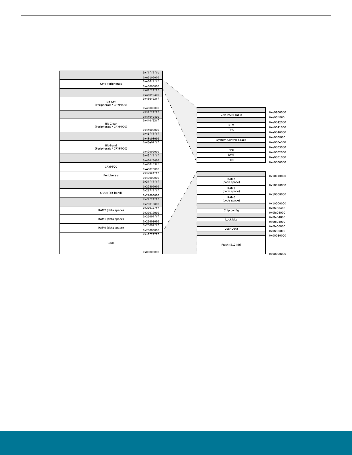
3.12 Memory Map
The BGM13P memory map is shown in the figures below. RAM and flash sizes are for the largest memory configuration.
Figure 3.3. BGM13P Memory Map — Core Peripherals and Code Space
silabs.com | Building a more connected world. Rev. 1.0 | 15

BGM13P Blue Gecko Bluetooth ® Module Data Sheet
System Overview
Figure 3.4. BGM13P Memory Map — Peripherals
3.13 Configuration Summary
The features of the BGM13P are a subset of the feature set described in the device reference manual. The table below describes device specific implementation of the features. Remaining modules support full configuration.
Table 3.3. Configuration Summary
Module Configuration Pin Connections
USART0 IrDA SmartCard US0_TX, US0_RX, US0_CLK, US0_CS
USART1
IrDA I2S SmartCard
US1_TX, US1_RX, US1_CLK, US1_CS
USART2 IrDA SmartCard US2_TX, US2_RX, US2_CLK, US2_CS
TIMER0 with DTI TIM0_CC[2:0], TIM0_CDTI[2:0]
TIMER1 - TIM1_CC[3:0]
WTIMER0 with DTI WTIM0_CC[2:0], WTIM0_CDTI[2:0]
silabs.com | Building a more connected world. Rev. 1.0 | 16

BGM13P Blue Gecko Bluetooth ® Module Data Sheet
Electrical Specifications
4. Electrical Specifications
4.1 Electrical Characteristics
All electrical parameters in all tables are specified under the following conditions, unless stated otherwise:
• Typical values are based on T
• Radio performance numbers are measured in conducted mode, based on Silicon Laboratories reference designs using output power-specific external RF impedance-matching networks for interfacing to a 50 Ω antenna.
• Minimum and maximum values represent the worst conditions across supply voltage, process variation, and operating temperature,
unless stated otherwise.
The BGM13P module has only one external supply pin (VDD). There are several internal supply rails mentioned in the electrical specifications, whose connections vary based on transmit power configuration. Refer to for the relationship between the module's external
VDD pin and internal voltage supply rails.
Refer to for more details about operational supply and temperature limits.
=25 °C and VDD= 3.3 V, by production test and/or technology characterization.
AMB
silabs.com | Building a more connected world. Rev. 1.0 | 17

BGM13P Blue Gecko Bluetooth ® Module Data Sheet
Electrical Specifications
4.1.1 Absolute Maximum Ratings
Stresses above those listed below may cause permanent damage to the device. This is a stress rating only and functional operation of
the devices at those or any other conditions above those indicated in the operation listings of this specification is not implied. Exposure
to maximum rating conditions for extended periods may affect device reliability. For more information on the available quality and reliability data, see the Quality and Reliability Monitor Report at http://www.silabs.com/support/quality/pages/default.aspx.
Table 4.1. Absolute Maximum Ratings
Parameter Symbol Test Condition Min Typ Max Unit
Storage temperature range T
Voltage on any supply pin V
Voltage ramp rate on any
supply pin
DC voltage on any GPIO pin V
Maximum RF level at input P
Total current into supply pins I
Total current into VSS
ground lines
Current per I/O pin I
Current for all I/O pins I
Junction temperature T
STG
DDMAX
V
DDRAMPMAX
DIGPIN
RFMAX2G4
VDDMAX
I
VSSMAX
IOMAX
IOALLMAX
J
-40 — 85 °C
-0.3 — 3.8 V
— — 1 V / µs
5V tolerant GPIO pins1 2
3
-0.3 — Min of 5.25
V
and IOVDD
+2
Standard GPIO pins -0.3 — IOVDD+0.3 V
— — 10 dBm
Source — — 200 mA
Sink — — 200 mA
Sink — — 50 mA
Source — — 50 mA
Sink — — 200 mA
Source — — 200 mA
-40 — 105 °C
Note:
1. When a GPIO pin is routed to the analog module through the APORT, the maximum voltage = IOVDD.
2. Valid for IOVDD in valid operating range or when IOVDD is undriven (high-Z). If IOVDD is connected to a low-impedance source
below the valid operating range (e.g. IOVDD shorted to VSS), the pin voltage maximum is IOVDD + 0.3 V, to avoid exceeding the
maximum IO current specifications.
3. To operate above the IOVDD supply rail, over-voltage tolerance must be enabled according to the GPIO_Px_OVTDIS register.
Pins with over-voltage tolerance disabled have the same limits as Standard GPIO.
silabs.com | Building a more connected world. Rev. 1.0 | 18

BGM13P Blue Gecko Bluetooth ® Module Data Sheet
Electrical Specifications
4.1.2 Operating Conditions
The following subsections define the operating conditions for the module.
4.1.2.1 General Operating Conditions
Table 4.2. General Operating Conditions
Parameter Symbol Test Condition Min Typ Max Unit
Operating ambient temperature range
VDD operating supply voltage
HFCORECLK frequency f
HFCLK frequency f
T
A
V
VDD
CORE
HFCLK
-G temperature grade -40 25 85 °C
DCDC in regulation 2.4 3.3 3.8 V
DCDC in bypass, 50mA load 1.8 3.3 3.8 V
VSCALE2, MODE = WS1 — — 40 MHz
VSCALE0, MODE = WS0 — — 20 MHz
VSCALE2 — — 40 MHz
VSCALE0 — — 20 MHz
silabs.com | Building a more connected world. Rev. 1.0 | 19

BGM13P Blue Gecko Bluetooth ® Module Data Sheet
Electrical Specifications
4.1.3 DC-DC Converter
Test conditions: V_DCDC_I=3.3 V, V_DCDC_O=1.8 V, I_DCDC_LOAD=50 mA, Heavy Drive configuration, F_DCDC_LN=7 MHz, unless otherwise indicated.
Table 4.3. DC-DC Converter
Parameter Symbol Test Condition Min Typ Max Unit
Input voltage range V
DCDC_I
Bypass mode, I
DCDC_LOAD
= 50
mA
Low noise (LN) mode, 1.8 V output, I
DCDC_LOAD
= 100 mA, or
1.8 — V
2.4 — V
VREGVDD_
MAX
VREGVDD_
MAX
Low power (LP) mode, 1.8 V out-
Output voltage programmable range
1
Max load current I
V
DCDC_O
LOAD_MAX
put, I
DCDC_LOAD
Low noise (LN) mode, Medium or
Heavy Drive
Low noise (LN) mode, Light
2
Drive
Low power (LP) mode,
2
= 10 mA
1.8 — V
VREGVDD
— — 70 mA
— — 50 mA
— — 75 µA
LPCMPBIASEMxx3 = 0
Low power (LP) mode,
— — 10 mA
LPCMPBIASEMxx3 = 3
Note:
1. Due to internal dropout, the DC-DC output will never be able to reach its input voltage, V
VREGVDD
.
2. Drive levels are defined by configuration of the PFETCNT and NFETCNT registers. Light Drive: PFETCNT=NFETCNT=3; Medium Drive: PFETCNT=NFETCNT=7; Heavy Drive: PFETCNT=NFETCNT=15.
3. LPCMPBIASEMxx refers to either LPCMPBIASEM234H in the EMU_DCDCMISCCTRL register or LPCMPBIASEM01 in the
EMU_DCDCLOEM01CFG register, depending on the energy mode.
V
V
V
silabs.com | Building a more connected world. Rev. 1.0 | 20

BGM13P Blue Gecko Bluetooth ® Module Data Sheet
Electrical Specifications
4.1.4 Current Consumption
4.1.4.1 Current Consumption 3.3 V using DC-DC Converter
Unless otherwise indicated, typical conditions are: VDD = 3.3 V. T = 25 °C. Minimum and maximum values in this table represent the
worst conditions across supply voltage and process variation at T = 25 °C.
Table 4.4. Current Consumption 3.3 V using DC-DC Converter
Parameter Symbol Test Condition Min Typ Max Unit
Current consumption in EM0
mode with all peripherals disabled, DCDC in Low Noise
DCM mode
2
Current consumption in EM0
mode with all peripherals disabled, DCDC in Low Noise
CCM mode
1
I
ACTIVE_DCM
I
ACTIVE_CCM
38.4 MHz crystal, CPU running
while loop from flash
4
38 MHz HFRCO, CPU running
Prime from flash
38 MHz HFRCO, CPU running
while loop from flash
38 MHz HFRCO, CPU running
CoreMark from flash
26 MHz HFRCO, CPU running
while loop from flash
1 MHz HFRCO, CPU running
while loop from flash
38.4 MHz crystal, CPU running
while loop from flash
4
38 MHz HFRCO, CPU running
Prime from flash
38 MHz HFRCO, CPU running
while loop from flash
38 MHz HFRCO, CPU running
CoreMark from flash
— 87 — µA/MHz
— 69 — µA/MHz
— 70 — µA/MHz
— 82 — µA/MHz
— 76 — µA/MHz
— 615 — µA/MHz
— 97 — µA/MHz
— 80 — µA/MHz
— 81 — µA/MHz
— 92 — µA/MHz
Current consumption in EM0
mode with all peripherals disabled and voltage scaling
enabled, DCDC in Low
Noise CCM mode
1
Current consumption in EM1
mode with all peripherals disabled, DCDC in Low Noise
DCM mode
2
Current consumption in EM1
mode with all peripherals disabled and voltage scaling
enabled, DCDC in Low
Noise DCM mode
2
I
ACTIVE_CCM_VS
I
EM1_DCM
I
EM1_DCM_VS
26 MHz HFRCO, CPU running
— 94 — µA/MHz
while loop from flash
1 MHz HFRCO, CPU running
— 1145 — µA/MHz
while loop from flash
19 MHz HFRCO, CPU running
— 101 — µA/MHz
while loop from flash
1 MHz HFRCO, CPU running
— 1124 — µA/MHz
while loop from flash
38.4 MHz crystal
4
— 56 — µA/MHz
38 MHz HFRCO — 39 — µA/MHz
26 MHz HFRCO — 46 — µA/MHz
1 MHz HFRCO — 588 — µA/MHz
19 MHz HFRCO — 50 — µA/MHz
1 MHz HFRCO — 572 — µA/MHz
silabs.com | Building a more connected world. Rev. 1.0 | 21

BGM13P Blue Gecko Bluetooth ® Module Data Sheet
Electrical Specifications
Parameter Symbol Test Condition Min Typ Max Unit
Current consumption in EM2
mode, with voltage scaling
enabled, DCDC in LP mode
3
I
EM2_VS
Full 64 kB RAM retention and
RTCC running from LFXO
Full 64 kB RAM retention and
— 1.4 — µA
— 1.5 — µA
RTCC running from LFRCO
Current consumption in EM3
mode, with voltage scaling
enabled
Current consumption in
EM4H mode, with voltage
scaling enabled
I
EM3_VS
I
EM4H_VS
1 bank RAM retention and RTCC
running from LFRCO
5
Full 64 kB RAM retention and
CRYOTIMER running from ULFRCO
128 byte RAM retention, RTCC
running from LFXO
128 byte RAM retention, CRYO-
— 1.3 — µA
— 1.14 — µA
— 0.75 — µA
— 0.44 — µA
TIMER running from ULFRCO
128 byte RAM retention, no RTCC — 0.42 — µA
Current consumption in
I
EM4S
No RAM retention, no RTCC — 0.07 — µA
EM4S mode
Note:
1. DCDC Low Noise CCM Mode = Light Drive (PFETCNT=NFETCNT=3), F=6.4 MHz (RCOBAND=4), ANASW=DVDD.
2. DCDC Low Noise DCM Mode = Light Drive (PFETCNT=NFETCNT=3), F=3.0 MHz (RCOBAND=0), ANASW=DVDD.
3. DCDC Low Power Mode = Medium Drive (PFETCNT=NFETCNT=7), LPOSCDIV=1, LPCMPBIASEM234H=0, LPCLIMILIMSEL=1, ANASW=DVDD.
4. CMU_HFXOCTRL_LOWPOWER=0.
5. CMU_LFRCOCTRL_ENVREF = 1, CMU_LFRCOCTRL_VREFUPDATE = 1
silabs.com | Building a more connected world. Rev. 1.0 | 22

BGM13P Blue Gecko Bluetooth ® Module Data Sheet
Electrical Specifications
4.1.4.2 Current Consumption Using Radio
Unless otherwise indicated, typical conditions are: VBATT = 3.3 V. T = 25 °C. DC-DC on. Minimum and maximum values in this table
represent the worst conditions across supply voltage and process variation at T = 25 °C.
Table 4.5. Current Consumption Using Radio
Parameter Symbol Test Condition Min Typ Max Unit
Current consumption in receive mode, active packet
reception (MCU in EM1 @
38.4 MHz, peripheral clocks
disabled), T ≤ 85 °C
Current consumption in receive mode, listening for
packet (MCU in EM1 @ 38.4
MHz, peripheral clocks disabled), T ≤ 85 °C
Current consumption in
transmit mode (MCU in EM1
@ 38.4 MHz, peripheral
clocks disabled), T ≤ 85 °C
I
RX_ACTIVE
I
RX_LISTEN
I
TX
125 kbit/s, 2GFSK, F = 2.4 GHz,
Radio clock prescaled by 4
500 kbit/s, 2GFSK, F = 2.4 GHz,
Radio clock prescaled by 4
1 Mbit/s, 2GFSK, F = 2.4 GHz,
Radio clock prescaled by 4
2 Mbit/s, 2GFSK, F = 2.4 GHz,
Radio clock prescaled by 4
125 kbit/s, 2GFSK, F = 2.4 GHz,
No radio clock prescaling
500 kbit/s, 2GFSK, F = 2.4 GHz,
No radio clock prescaling
1 Mbit/s, 2GFSK, F = 2.4 GHz, No
radio clock prescaling
2 Mbit/s, 2GFSK, F = 2.4 GHz, No
radio clock prescaling
F = 2.4 GHz, CW, 0 dBm output
power, Radio clock prescaled by 3
F = 2.4 GHz, CW, 0 dBm output
power, Radio clock prescaled by 1
— 10.5 — mA
— 10.4 — mA
— 9.9 — mA
— 10.6 — mA
— 10.5 — mA
— 10.5 — mA
— 10.9 — mA
— 11.6 — mA
— 8.5 — mA
— 9.6 — mA
F = 2.4 GHz, CW, 3.5 dBm output
power
F = 2.4 GHz, CW, 8 dBm output
power
— 20.2 —
— 27.1 — mA
silabs.com | Building a more connected world. Rev. 1.0 | 23

BGM13P Blue Gecko Bluetooth ® Module Data Sheet
Electrical Specifications
4.1.5 Wake Up Times
Table 4.6. Wake Up Times
Parameter Symbol Test Condition Min Typ Max Unit
Wakeup time from EM1 t
Wake up from EM2 t
EM1_WU
EM2_WU
Code execution from flash — 10.9 — µs
— 3 — AHB
Code execution from RAM — 3.8 — µs
Wake up from EM3 t
EM3_WU
Code execution from flash — 10.9 — µs
Code execution from RAM — 3.8 — µs
Wake up from EM4H
Wake up from EM4S
1
1
Time from release of reset
source to first instruction execution
Power mode scaling time t
t
EM4H_WU
t
EM4S_WU
t
RESET
SCALE
Executing from flash — 90 — µs
Executing from flash — 300 — µs
Soft Pin Reset released — 51 — µs
Any other reset released — 358 — µs
VSCALE0 to VSCALE2, HFCLK =
19 MHz4
2
VSCALE2 to VSCALE0, HFCLK =
19 MHz
3
— 31.8 — µs
— 4.3 — µs
Note:
1. Time from wakeup request until first instruction is executed. Wakeup results in device reset.
2. VSCALE0 to VSCALE2 voltage change transitions occur at a rate of 10 mV/µs for approximately 20 µs. During this transition,
peak currents will be dependent on the value of the DECOUPLE output capacitor, from 35 mA (with a 1 µF capacitor) to 70 mA
(with a 2.7 µF capacitor).
3. Scaling down from VSCALE2 to VSCALE0 requires approximately 2.8 µs + 29 HFCLKs.
4. Scaling up from VSCALE0 to VSCALE2 requires approximately 30.3 µs + 28 HFCLKs.
Clocks
4.1.6 Brown Out Detector (BOD)
Table 4.7. Brown Out Detector (BOD)
Parameter Symbol Test Condition Min Typ Max Unit
AVDD BOD threshold V
AVDDBOD
AVDD rising — — 1.8 V
AVDD falling (EM0/EM1) 1.62 — — V
AVDD falling (EM2/EM3) 1.53 — — V
AVDD BOD hysteresis V
AVDD BOD response time t
EM4 BOD threshold V
AVDDBOD_HYST
AVDDBOD_DELAY
EM4DBOD
Supply drops at 0.1V/µs rate — 2.4 — µs
AVDD rising — — 1.7 V
— 20 — mV
AVDD falling 1.45 — — V
EM4 BOD hysteresis V
EM4 BOD response time t
silabs.com | Building a more connected world. Rev. 1.0 | 24
EM4BOD_HYST
EM4BOD_DELAY
Supply drops at 0.1V/µs rate — 300 — µs
— 25 — mV

BGM13P Blue Gecko Bluetooth ® Module Data Sheet
Electrical Specifications
4.1.7 Frequency Synthesizer
Table 4.8. Frequency Synthesizer
Parameter Symbol Test Condition Min Typ Max Unit
RF synthesizer frequency
range
LO tuning frequency resolution with 38.4 MHz crystal
Frequency deviation resolution with 38.4 MHz crystal
Maximum frequency deviation with 38.4 MHz crystal
f
RANGE
f
RES
df
RES
df
MAX
2400 - 2483.5 MHz 2400 — 2483.5 MHz
2400 - 2483.5 MHz — — 73 Hz
2400 - 2483.5 MHz — — 73 Hz
2400 - 2483.5 MHz — — 1677 kHz
silabs.com | Building a more connected world. Rev. 1.0 | 25

BGM13P Blue Gecko Bluetooth ® Module Data Sheet
Electrical Specifications
4.1.8 2.4 GHz RF Transceiver Characteristics
4.1.8.1 RF Transmitter General Characteristics for 2.4 GHz Band
Unless otherwise indicated, typical conditions are: T = 25 °C, VDD = 3.3 V. DC-DC on. Crystal frequency=38.4 MHz. RF center frequency 2.45 GHz. Conducted measurement from the antenna feedpoint.
Table 4.9. RF Transmitter General Characteristics for 2.4 GHz Band
Parameter Symbol Test Condition Min Typ Max Unit
Maximum TX power
1
POUT
MAX
8 dBm-rated part numbers — 8 — dBm
Minimum active TX Power POUT
Output power step size POUT
Output power variation vs
supply at POUT
MAX
Output power variation vs
temperature at POUT
MAX
Output power variation vs RF
frequency at POUT
MAX
RF tuning frequency range F
POUT
POUT
POUT
RANGE
MIN
STEP
VAR_V
VAR_T
VAR_F
CW -27 — dBm
-5 dBm< Output power < 0 dBm — 0.8 — dB
0 dBm < output power <
POUT
MAX
2.4 V < V
< 3.3 V, BGM13P22 — 0.05 — dB
VDD
— 0.5 — dB
From -40 to +85 °C, BGM13P22 — 1.7 — dB
Over RF tuning frequency range — 0.3 — dB
2400 — 2483.5 MHz
Note:
1. Supported transmit power levels are determined by the ordering part number (OPN). Transmit power ratings for all devices covered in this datasheet can be found in the Max TX Power column of the Ordering Information Table.
4.1.8.2 RF Receiver General Characteristics for 2.4 GHz Band
Unless otherwise indicated, typical conditions are: T = 25 °C, VDD = 3.3 V. DC-DC on. Crystal frequency=38.4 MHz. RF center frequency 2.45 GHz. Conducted measurement from the antenna feedpoint.
Table 4.10. RF Receiver General Characteristics for 2.4 GHz Band
Parameter Symbol Test Condition Min Typ Max Unit
RF tuning frequency range F
Receive mode maximum
spurious emission
Max spurious emissions during active receive mode, per
FCC Part 15.109(a)
RANGE
SPUR
SPUR
RX
RX_FCC
30 MHz to 1 GHz — -87.3 — dBm
1 GHz to 12 GHz — -81.0 — dBm
216 MHz to 960 MHz, Conducted
Measurement
Above 960 MHz, Conducted
2400 — 2483.5 MHz
— -84.2 — dBm
— -73.1 — dBm
Measurement
silabs.com | Building a more connected world. Rev. 1.0 | 26

BGM13P Blue Gecko Bluetooth ® Module Data Sheet
Electrical Specifications
4.1.8.3 RF Receiver Characteristics for Bluetooth Low Energy in the 2.4GHz Band, 125 kbps Data Rate
Unless otherwise indicated, typical conditions are: T = 25 °C, VDD = 3.3 V. DC-DC on. Crystal frequency=38.4 MHz. RF center frequency 2.45 GHz. Conducted measurement from the antenna feedpoint.
Table 4.11. RF Receiver Characteristics for Bluetooth Low Energy in the 2.4GHz Band, 125 kbps Data Rate
Parameter Symbol Test Condition Min Typ Max Unit
Sensitivity, 0.1% BER SENS
Signal is reference signal1. Using
— -103.2 — dBm
DC-DC converter.
With non-ideal signals as speci-
— -102.8 — dBm
fied in RF-PHY.TS.4.2.2, section
4.6.1.
Note:
1. Reference signal is defined 2GFSK at -67 dBm, Modulation index = 0.5, BT = 0.5, Bit rate = 125 kbps, desired data = PRBS9;
interferer data = PRBS15; frequency accuracy better than 1 ppm.
4.1.8.4 RF Receiver Characteristics for Bluetooth Low Energy in the 2.4GHz Band, 500 kbps Data Rate
Unless otherwise indicated, typical conditions are: T = 25 °C, VDD = 3.3 V. DC-DC on. Crystal frequency=38.4 MHz. RF center frequency 2.45 GHz. Conducted measurement from the antenna feedpoint.
Table 4.12. RF Receiver Characteristics for Bluetooth Low Energy in the 2.4GHz Band, 500 kbps Data Rate
Parameter Symbol Test Condition Min Typ Max Unit
Sensitivity, 0.1% BER SENS
Signal is reference signal1. Using
— -98.8 — dBm
DC-DC converter.
With non-ideal signals as speci-
— -97.6 — dBm
fied in RF-PHY.TS.4.2.2, section
4.6.1.
Note:
1. Reference signal is defined 2GFSK at -67 dBm, Modulation index = 0.5, BT = 0.5, Bit rate = 500 kbps, desired data = PRBS9;
interferer data = PRBS15; frequency accuracy better than 1 ppm.
4.1.8.5 RF Receiver Characteristics for Bluetooth Low Energy in the 2.4GHz Band, 1 Mbps Data Rate
Unless otherwise indicated, typical conditions are: T = 25 °C, VDD = 3.3 V. DC-DC on. Crystal frequency=38.4 MHz. RF center frequency 2.45 GHz. Conducted measurement from the antenna feedpoint.
Table 4.13. RF Receiver Characteristics for Bluetooth Low Energy in the 2.4GHz Band, 1 Mbps Data Rate
Parameter Symbol Test Condition Min Typ Max Unit
Sensitivity, 0.1% BER SENS
Signal is reference signal1. Using
— -95 — dBm
DC-DC converter.
With non-ideal signals as speci-
— -94.8 — dBm
fied in RF-PHY.TS.4.2.2, section
4.6.1.
Note:
1. Reference signal is defined 2GFSK at -67 dBm, Modulation index = 0.5, BT = 0.5, Bit rate = 1 Mbps, desired data = PRBS9;
interferer data = PRBS15; frequency accuracy better than 1 ppm.
silabs.com | Building a more connected world. Rev. 1.0 | 27

BGM13P Blue Gecko Bluetooth ® Module Data Sheet
Electrical Specifications
4.1.8.6 RF Receiver Characteristics for Bluetooth Low Energy in the 2.4GHz Band, 2 Mbps Data Rate
Unless otherwise indicated, typical conditions are: T = 25 °C, VDD = 3.3 V. DC-DC on. Crystal frequency=38.4 MHz. RF center frequency 2.45 GHz. Conducted measurement from the antenna feedpoint.
Table 4.14. RF Receiver Characteristics for Bluetooth Low Energy in the 2.4GHz Band, 2 Mbps Data Rate
Parameter Symbol Test Condition Min Typ Max Unit
Sensitivity, 0.1% BER SENS
Signal is reference signal1. Using
— -91.2 — dBm
DC-DC converter.
With non-ideal signals as speci-
— -91.2 — dBm
fied in RF-PHY.TS.4.2.2, section
4.6.1.
Note:
1. Reference signal is defined 2GFSK at -67 dBm, Modulation index = 0.5, BT = 0.5, Bit rate = 2 Mbps, desired data = PRBS9;
interferer data = PRBS15; frequency accuracy better than 1 ppm.
silabs.com | Building a more connected world. Rev. 1.0 | 28

BGM13P Blue Gecko Bluetooth ® Module Data Sheet
Electrical Specifications
4.1.9 Oscillators
4.1.9.1 Low-Frequency Crystal Oscillator (LFXO)
Table 4.15. Low-Frequency Crystal Oscillator (LFXO)
Parameter Symbol Test Condition Min Typ Max Unit
Crystal frequency f
Overall frequency tolerance
in all conditions
1
LFXO
FT
LFXO
— 32.768 — kHz
-100 — 100 ppm
Note:
1. Nominal crystal frequency tolerance of ± 20 ppm.
4.1.9.2 High-Frequency Crystal Oscillator (HFXO)
Table 4.16. High-Frequency Crystal Oscillator (HFXO)
Parameter Symbol Test Condition Min Typ Max Unit
Crystal frequency f
HFXO
38.4 MHz required for radio trans-
— 38.4 — MHz
ciever operation
Frequency tolerance for the
FT
HFXO
-40 — 40 ppm
crystal
4.1.9.3 Low-Frequency RC Oscillator (LFRCO)
Table 4.17. Low-Frequency RC Oscillator (LFRCO)
Parameter Symbol Test Condition Min Typ Max Unit
Oscillation frequency f
Startup time t
Current consumption
1
LFRCO
LFRCO
I
LFRCO
ENVREF2 = 1
ENVREF2 = 0
ENVREF = 1 in
31.3 32.768 33.6 kHz
31.3 32.768 33.4 kHz
— 500 — µs
— 342 — nA
CMU_LFRCOCTRL
ENVREF = 0 in
— 494 — nA
CMU_LFRCOCTRL
Note:
1. Block is supplied by AVDD if ANASW = 0, or DVDD if ANASW=1 in EMU_PWRCTRL register.
2. In CMU_LFRCOCTRL register.
silabs.com | Building a more connected world. Rev. 1.0 | 29
 Loading...