

Silicon Laboratories Finland BGM113 Users Manual
BGM113 Blue Gecko Bluetooth® Smart
Module Data Sheet
The Blue Gecko BGM113 is a Bluetooth® Smart Module targeted for Bluetooth Smart
applications where small size, reliable RF, low-power consumption, and easy application
development are key requirements. At +3 dBm TX power, BGM113 is ideal for applications requiring short and medium range Bluetooth Smart connectivity.
The BGM113 integrates all of the necessary elements required for a Bluetooth Smart application: Bluetooth radio, software stack, and GATT-based profiles, and it can also host
end user applications, which means no external microcontroller is required in size, price
or power constrained devices. The BGM113 Bluetooth Smart Module also has highly
flexible hardware interfaces to connect to different peripherals or sensors.
BGM113 can be used in a wide variety of applications:
• IoT Sensors and End Devices
• Commercial and Retail
•
Health and Wellness
• Industrial, Home and Building Automation
• Smart Phone, Tablet and PC Accessories
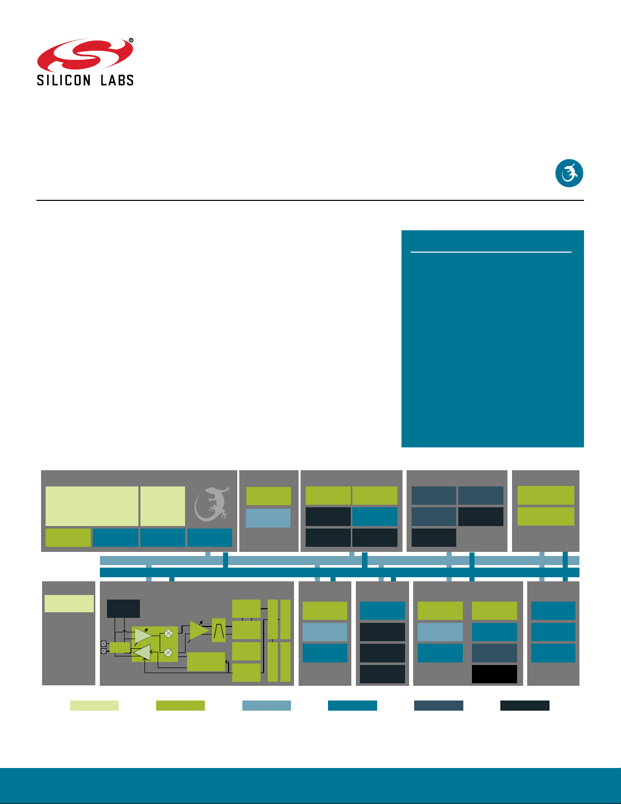
32.768kHz XTAL
DEMOD
IFADC
AGC
MOD
Clocks
38.4MHz XTAL
FRC
CRC
Clock Management
High Frequency
Crystal Oscillator
Low Frequency
RC Oscillator
Low Frequency
Crystal Oscillator
32-bit bus
Peripheral Reflex System
Serial
Interfaces
USART
BUFC
Low Energy
UART
I2C
RAC
High Frequency
RC Oscillator
Auxiliary High
Frequency
RC Oscillator
Ultra Low
Frequency
RC Oscillator
I/O Ports Analog I/F
External Interrupts
General Purpose
I/O
Pin Reset
Pin Wakeup
ARM Cortex M4 processor
with DSP extensions and FPU
Flash Program
Memory
RAM Memory Debug Interface DMA Controller
Antenna
Chip Antenna
Core / Memory
Memory Protection
RFSENSE
LNA
BALUN
RF Frontend
PA
Unit
Radio Transceiver
PGA
I
Frequency
Q
Synthesizer
KEY FEATURES
• Bluetooth 4.1 Compliant (Bluetooth Smart)
• Software upgradable to Bluetooth 4.2
•
Integrated antenna
• TX power: up to +3 dBm
• RX sensitivity: down to -93 dBm
• Range: up to 50 meters
• 32-bit ARM® Cortex®-M4 core at 38.4
MHz
• Flash memory: 256kB
• RAM: 32 kB
• Autonomous Hardware Crypto Accelerator
and True Random Number Generator
• Integrated DC-DC Converter
• Onboard Bluetooth Smart stack
Energy Management
Voltage
Regulator
DC-DC
Converter
Brown-Out
Detector
Voltage Monitor
Power-On Reset
Timers and Triggers
Timer/Counter
Low Energy
Timer
Pulse Counter
Watchdog Timer
Real Time Counter
and Calendar
Protocol Timer
Cryotimer
Other
CRYPTO
CRC
ADC
Analog
Comparator
IDAC
Lowest power mode with peripheral operational:
EM3—StopEM2—Deep SleepEM1—Sleep EM4—Hibernate EM4—ShutoffEM0—Active
silabs.com | Smart. Connected. Energy-friendly. Preliminary Rev. 0.93
This information applies to a product under development. Its characteristics and specifications are subject to change without notice.

1. Feature List
The BGM113 highlighted features are listed below.
• Low Power Wireless System-on-Chip.
•
High Performance 32-bit 38.4 MHz ARM Cortex®-M4 with
DSP instruction and floating-point unit for efficient signal
processing
•
256 kB flash program memory
• 32 kB RAM data memory
• 2.4 GHz radio operation
• TX power up to +3 dBm
• Low Energy Consumption
• 8.7 mA RX current at 2.4 GHz
• 8.8 mA TX current @ 0 dBm output power at 2.4 GHz
• 63 μA/MHz in Active Mode (EM0)
• 1.4 μA EM2 DeepSleep current (full RAM retention and
RTCC running from LFXO)
• 1.1 μA EM3 Stop current (State/RAM retention)
• Wake on Radio with signal strength detection, preamble
pattern detection, frame detection and timeout
• High Receiver Performance
• -93 dBm sensitivity @ 1 Mbit/s GFSK (2.4GHz)
• Supported Protocol
•
Bluetooth® Smart
• Support for Internet Security
• General Purpose CRC
• Random Number Generator
• Hardware Cryptographic Acceleration for AES 128/256,
SHA-1, SHA-2 (SHA-224 and SHA-256) and ECC
BGM113 Blue Gecko Bluetooth® Smart Module
Data Sheet
Feature List
• Wide selection of MCU peripherals
•
12-bit 1 Msps SAR Analog to Digital Converter (ADC)
• 2× Analog Comparator (ACMP)
• Digital to Analog Current Converter (IDAC)
• 14 pins connected to analog channels (APORT) shared between Analog Comparators, ADC, and IDAC
• 14 General Purpose I/O pins with output state retention and
asynchronous interrupts
• 8 Channel DMA Controller
• 12 Channel Peripheral Reflex System (PRS)
• 2×16-bit Timer/Counter
• 3 + 4 Compare/Capture/PWM channels
• 32-bit Real Time Counter and Calendar
• 16-bit Low Energy Timer for waveform generation
• 32-bit Ultra Low Energy Timer/Counter for periodic wake-up
from any Energy Mode
• 16-bit Pulse Counter with asynchronous operation
• Watchdog Timer with dedicated RC oscillator @ 50nA
• 2×Universal Synchronous/Asynchronous Receiver/Transmitter (UART/SPI/SmartCard (ISO 7816)/IrDA/I2S)
•
Low Energy UART (LEUART™)
•
I2C interface with SMBus support and address recognition
in EM3 Stop
• Wide Operating Range
• 1.85 V to 3.8 V single power supply
• Integrated DC-DC
• -40 °C to 85 °C
• Dimensions
• 9.15 x 15.73 x 1.9 mm
silabs.com | Smart. Connected. Energy-friendly. Preliminary Rev. 0.93 | 1

2. Ordering Information
BGM113 Blue Gecko Bluetooth® Smart Module Data Sheet
Ordering Information
Ordering Code Protocol Stack Frequency
Band
Max TX
Power
Encryption Flash
(KB)
RAM
(KB)
GPIO Package
(dBm)
BGM113A256V1
1
Bluetooth Smart 2.4 GHz 3 Full 256 32 14 100 pcs
cut reel
BGM113A256V1R
1
Bluetooth Smart 2.4 GHz 3 Full 256 32 14 1000 pcs
tape and
reel
BGM113A256V2 Bluetooth Smart 2.4 GHz 3 Full 256 32 14 100 pcs
cut reel
BGM113A256V2R Bluetooth Smart 2.4 GHz 3 Full 256 32 14 1000 pcs
tape and
reel
SLWSTK6101B
2
Note:
Initial production. This (V1) product code is updated to production version (V2) when the logos of the official CE and FCC certifi-
1.
cations are marked into the RF shield. The only visual difference between initial production (V1) and production (V2) versions will
be the certification codes printed on the RF shield. Silicon Labs reserves the right to deliver V2 (production version) for customers
ordering V1.
2.
Blue Gecko Bluetooth Smart Module Wireless Development Kit (WSTK) with BGM113 and BGM111 radio boards, expansion
board and accessories.
silabs.com | Smart. Connected. Energy-friendly. Preliminary Rev. 0.93 | 2
BGM113 Blue Gecko Bluetooth® Smart Module Data Sheet
System Overview
3. System Overview
3.1 Introduction
The BGM113 product family combines an energy-friendly MCU with a highly integrated radio transceiver. The devices are well suited
for any battery operated application, as well as other system requiring high performance and low-energy consumption. This section
gives a short introduction to the full radio and MCU system. The detailed functional description can be found in the EFR32 Reference
Manual.
A detailed block diagram of the EFR32BG SoC is shown in the figure below which is used in the BGM113 Bluetooth Smart module.
2G4RF_IOP
2G4RF_ION
PAVDD
RFVDD
IOVDD
AVDD
DVDD
VREGVDD
VREGSW
DECOUPLE
VSS
VREGVSS
RFVSS
PAVSS
RESETn
HFXTAL_P
HFXTAL_N
RFSENSE
BALUN
RF Frontend
LNA
PA
Energy Management
bypass
DC-DC
Converter
Voltage
Regulator
Management
LFXTAL_P / N
Radio Transciever
PGA
I
Frequency
Q
Synthesizer
Voltage
Monitor
Brown Out /
Power-On
Reset
Reset
Unit
DEMOD
IFADC
AGC
MOD
FRC
CRC
ARM Cortex-M4 Core
Up to 256 KB ISP Flash
Program Memory
Up to 32 KB RAM
Memory Protection Unit
Floating Point Unit
DMA Controller
Serial Wire Debug /
Programming
Watchdog
Timer
Clock Management
ULFRCO
AUXHFRCO
LFRCO
HFRCO
LFXO
HFXO
BUFC
RAC
Port I/O Configuration
Digital Peripherals
LETIMER
TIMER
CRYOTIMER
PCNT
RTC / RTCC
USART
LEUART
I2C
A
H
B
CRYPTO
A
P
B
CRC
Port
Mapper
Analog Peripherals
Internal
Reference
12-bit ADC
Analog Comparator
IDAC
VREFVDD
VDD
Input MUX
Sensor
+
-
Temp
APORT
IOVDD
Port A
Drivers
Port B
Drivers
Port C
Drivers
Port D
Drivers
Port F
Drivers
PAn
PBn
PCn
PDn
PFn
Figure 3.1. Detailed EFR32BG1 Block Diagram
3.2 Radio
The BGM113 features a radio transceiver supporting Bluetooth Smart® protocol.
3.2.1 Antenna Interface
The BGM113
has a built in 2.4GHz ceramic chip antenna.
Table 3.1. Antenna Efficiency and Peak Gain
Parameter With optimal layout Note
Efficiency 30% Efficiency and peak gain depend on the application PCB layout
Peak gain 0.5 dBi
silabs.com | Smart. Connected. Energy-friendly. Preliminary Rev. 0.93 | 3
and mechanical design

3.2.2 Wake on Radio
BGM113 Blue Gecko Bluetooth® Smart Module Data Sheet
System Overview
The Wake
on Radio feature allows flexible, autonomous RF sensing, qualification, and demodulation without required MCU activity, us-
ing a subsystem of the BGM113 including the Radio Controller (RAC), Peripheral Reflex System (PRS), and Low Energy peripherals.
3.2.3 RFSENSE
The RFSENSE module generates a system wakeup interrupt upon detection of wideband RF energy at the antenna interface, providing
true RF wakeup capabilities from low energy modes including EM2, EM3 and EM4.
RFSENSE triggers on a relatively strong RF signal and is available in the lowest energy modes, allowing exceptionally low energy consumption. RFSENSE does not demodulate or otherwise qualify the received signal, but software may respond to the wakeup event by
enabling normal RF reception.
Various strategies for optimizing power consumption and system response time in presence of false alarms may be employed using
available timer peripherals.
3.2.4 Packet and State Trace
The BGM113 Frame Controller has a packet and state trace unit that provides valuable information during the development phase. It
features:
• Non-intrusive trace of transmit data, receive data and state information
• Data observability on a single-pin UART data output, or on a two-pin SPI data output
• Configurable data output bitrate / baudrate
• Multiplexed transmitted data, received data and state / meta information in a single serial data stream
3.2.5 Data Buffering
The BGM113 features an advanced Radio Buffer Controller (BUFC) capable of handling up to 4 buffers of adjustable size from 64 bytes
to 4096 bytes. Each buffer can be used for RX, TX or both. The buffer data is located in RAM, enabling zero-copy operations.
3.2.6 Radio Controller (RAC)
The Radio Controller controls the top level state of the radio subsystem in the BGM113. It performs the following tasks:
• Precisely-timed control of enabling and disabling of the receiver and transmitter circuitry
• Run-time calibration of receiver, transmitter and frequency synthesizer
• Detailed frame transmission timing, including optional LBT or CSMA-CA
3.2.7 Random Number Generator
The Frame Controller (FRC) implements a random number generator that uses entropy gathered from noise in the RF receive chain.
The data is suitable for use in cryptographic applications.
Output from the random number generator can be used either directly or as a seed or entropy source for software-based random number generator algorithms such as Fortuna.
silabs.com | Smart. Connected. Energy-friendly. Preliminary Rev. 0.93 | 4

3.3 Power
BGM113 Blue Gecko Bluetooth®
Smart Module
Data Sheet
System Overview
The BGM113 has
an Energy Management Unit (EMU) and efficient integrated regulators to generate internal supply voltages. Only a
single external supply voltage is required, from which all internal voltages are created. An integrated DC-DC buck regulator is utilized to
further reduce the current consumption.
3.3.1 Energy Management Unit (EMU)
The Energy Management Unit manages transitions of energy modes in the device. Each energy mode defines which peripherals and
features are available and the amount of current the device consumes. The EMU can also be used to turn off the power to unused RAM
blocks, and it contains control registers for the dc-dc regulator and the Voltage Monitor (VMON). The VMON is used to monitor multiple
supply voltages. It has multiple channels which can be programmed individually by the user to determine if a sensed supply has fallen
below a chosen threshold.
3.3.2 DC-DC Converter
The DC-DC buck converter covers a wide range of load currents and provides up to 90% efficiency in energy modes EM0, EM1, EM2
and EM3. Patented RF noise mitigation allows operation of the DC-DC converter without degrading sensitivity of radio components.
Protection features include programmable current limiting, short-circuit protection, and dead-time protection. The DC-DC converter may
also enter bypass mode when the input voltage is too low for efficient operation. In bypass mode, the DC-DC input supply is internally
connected directly to its output through a low resistance switch. Bypass mode also supports in-rush current limiting to prevent input
supply voltage droops due to excessive output current transients.
3.4 General Purpose Input/Output (GPIO)
BGM113 has up to 14 General Purpose Input/Output pins. Each GPIO pin can be individually configured as either an output or input.
More advanced configurations including open-drain, open-source, and glitch-filtering can be configured for each individual GPIO pin.
The GPIO pins can be overridden by peripheral connections, like SPI communication. Each peripheral connection can be routed to several GPIO pins on the device. The input value of a GPIO pin can be routed through the Peripheral Reflex System to other peripherals.
The GPIO subsystem supports asynchronous external pin interrupts.
3.5 Clocking
3.5.1 Clock Management Unit (CMU)
The Clock Management Unit controls oscillators and clocks in the BGM113. Individual enabling and disabling of clocks to all peripheral
modules is perfomed by the CMU. The CMU also controls enabling and configuration of the oscillators. A high degree of flexibility allows software to optimize energy consumption in any specific application by minimizing power dissipation in unused peripherals and
oscillators.
3.5.2 Internal Oscillators
The BGM113 fully integrates two crystal oscillators and four RC oscillators, listed below.
• A 38.4MHz high frequency crystal oscillator (HFXO) provides a precise timing reference for the MCU and radio.
• A 32.768 kHz crystal oscillator (LFXO) provides an accurate timing reference for low energy modes.
• An integrated high frequency RC oscillator (HFRCO) is available for the MCU system, when crystal accuracy is not required. The
HFRCO employs fast startup at minimal energy consumption combined with a wide frequency range.
• An integrated auxilliary high frequency RC oscillator (AUXHFRCO) is available for timing the general-purpose ADC and the Serial
Wire debug port with a wide frequency range.
• An integrated low frequency 32.768 kHz RC oscillator (LFRCO) can be used as a timing reference in low energy modes, when crystal accuracy is not required.
• An integrated ultra-low frequency 1 kHz RC oscillator (ULFRCO) is available to provide a timing reference at the lowest energy consumption in low energy modes.
silabs.com | Smart. Connected. Energy-friendly. Preliminary Rev. 0.93 | 5

3.6 Counters/Timers and PWM
3.6.1 Timer/Counter (TIMER)
BGM113 Blue Gecko Bluetooth® Smart Module Data Sheet
System Overview
TIMER peripherals
keep track of timing, count events, generate PWM outputs and trigger timed actions in other peripherals through the
PRS system. The core of each TIMER is a 16-bit counter with up to 4 compare/capture channels. Each channel is configurable in one
of three modes. In capture mode, the counter state is stored in a buffer at a selected input event. In compare mode, the channel output
reflects the comparison of the counter to a programmed threshold value. In PWM mode, the TIMER supports generation of pulse-width
modulation (PWM) outputs of arbitrary waveforms defined by the sequence of values written to the compare registers, with optional
dead-time insertion available in timer unit TIMER_0 only.
3.6.2 Real Time Counter and Calendar (RTCC)
The Real Time Counter and Calendar (RTCC) is a 32-bit counter providing timekeeping in all energy modes. The RTCC includes a
Binary Coded Decimal (BCD) calendar mode for easy time and date keeping. The RTCC can be clocked by any of the on-board oscillators with the exception of the AUXHFRCO, and it is capable of providing system wake-up at user defined instances. When receiving
frames, the RTCC value can be used for timestamping. The RTCC includes 128 bytes of general purpose data retention, allowing easy
and convenient data storage in all energy modes.
3.6.3 Low Energy Timer (LETIMER)
The unique LETIMER is a 16-bit timer that is available in energy mode EM2 Deep Sleep in addition to EM1 Sleep and EM0 Active. This
allows it to be used for timing and output generation when most of the device is powered down, allowing simple tasks to be performed
while the power consumption of the system is kept at an absolute minimum. The LETIMER can be used to output a variety of waveforms with minimal software intervention. The LETIMER is connected to the Real Time Counter and Calendar (RTCC), and can be configured to start counting on compare matches from the RTCC.
3.6.4 Ultra Low Power Wake-up Timer (CRYOTIMER)
The CRYOTIMER is a 32-bit counter that is capable of running in all energy modes. It can be clocked by either the 32.768 kHz crystal
oscillator (LFXO), the 32.768 kHz RC oscillator (LFRCO), or the 1 kHz RC oscillator (ULFRCO). It can provide periodic Wakeup events
and PRS signals which can be used to wake up peripherals from any energy mode. The CRYOTIMER provides a wide range of interrupt periods, facilitating flexible ultra-low energy operation.
3.6.5 Pulse Counter (PCNT)
The Pulse Counter (PCNT) peripheral can be used for counting pulses on a single input or to decode quadrature encoded inputs. The
clock for PCNT is selectable from either an external source on pin PCTNn_S0IN or from an internal timing reference, selectable from
among any of the internal oscillators, except the AUXHFRCO. The module may operate in energy mode EM0 Active, EM1 Sleep, EM2
Deep Sleep, and EM3 Stop.
3.6.6 Watchdog Timer (WDOG)
The watchdog timer can act both as an independent watchdog or as a watchdog synchronous with the CPU clock. It has windowed
monitoring capabilities, and can generate a reset or different interrupts depending on the failure mode of the system. The watchdog can
also monitor autonomous systems driven by PRS.
3.7 Communications and Other Digital Peripherals
3.7.1 Universal Synchronous/Asynchronous Receiver/Transmitter (USART)
The Universal Synchronous/Asynchronous Receiver/Transmitter is a flexible serial I/O module. It supports full duplex asynchronous
UART communication with hardware flow control as well as RS-485, SPI, MicroWire and 3-wire. It can also interface with devices supporting:
• ISO7816 SmartCards
• IrDA
•
I2S
silabs.com | Smart. Connected. Energy-friendly. Preliminary Rev. 0.93 | 6

3.7.2 Low Energy Universal Asynchronous Receiver/Transmitter (LEUART)
BGM113 Blue Gecko Bluetooth® Smart Module
System Overview
Data Sheet
The unique
LEUARTTM provides two-way UART communication on a strict power budget. Only a 32.768 kHz clock is needed to allow
UART communication up to 9600 baud. The LEUART includes all necessary hardware to make asynchronous serial communication
possible with a minimum of software intervention and energy consumption.
3.7.3 Inter-Integrated Circuit Interface (I2C)
The I2C module provides an interface between the MCU and a serial I2C bus. It is capable of acting as both a master and a slave and
supports multi-master buses. Standard-mode, fast-mode and fast-mode plus speeds are supported, allowing transmission rates from 10
kbit/s up to 1 Mbit/s. Slave arbitration and timeouts are also available, allowing implementation of an SMBus-compliant system. The
interface provided to software by the I2C module allows precise timing control of the transmission process and highly automated transfers. Automatic recognition of slave addresses is provided in active and low energy modes.
3.7.4 Peripheral Reflex System (PRS)
The Peripheral Reflex System provides a communication network between different peripheral modules without software involvement.
Peripheral modules producing Reflex signals are called producers. The PRS routes Reflex signals from producers to consumer peripherals which in turn perform actions in response. Edge triggers and other functionality can be applied by the PRS. The PRS allows peripheral to act autonomously without waking the MCU core, saving power.
3.8 Security Features
3.8.1 GPCRC (General Purpose Cyclic Redundancy Check)
The GPCRC module implements a Cyclic Redundancy Check (CRC) function. It supports both 32-bit and 16-bit polynomials. The supported 32-bit polynomial is 0x04C11DB7 (IEEE 802.3), while the 16-bit polynomial can be programmed to any value, depending on the
needs of the application.
3.8.2 Crypto Accelerator (CRYPTO)
The Crypto Accelerator is a fast and energy-efficient autonomous hardware encryption and decryption accelerator. It supports AES encryption and decryption with 128- or 256-bit keys and ECC over both GF(P) and GF(2m), SHA-1 and SHA-2 (SHA-224 and SHA-256).
Supported modes of operation for AES include: ECB, CTR, CBC, PCBC, CFB, OFB, CBC-MAC, GMAC and CCM.
Supported ECC NIST recommended curves include P-192, P-224, P-256, K-163, K-233, B-163 and B-233.
The CRYPTO is tightly linked to the Radio Buffer Controller (BUFC) enabling fast and efficient autonomous cipher operations on data
buffer content. It allows fast processing of GCM (AES), ECC and SHA with little CPU intervention. CRYPTO also provides trigger signals for DMA read and write operations.
3.9 Analog
3.9.1 Analog Port (APORT)
The Analog Port (APORT) is an analog interconnect matrix allowing access to analog modules ADC, ACMP, and IDAC on a flexible
selection of pins. Each APORT bus consists of analog switches connected to a common wire. Since many clients can operate differentially, buses are grouped by X/Y pairs.
3.9.2 Analog Comparator (ACMP)
The Analog Comparator is used to compare the voltage of two analog inputs, with a digital output indicating which input voltage is higher. Inputs are selected from among internal references and external pins. The tradeoff between response time and current consumption
is configurable by software. Two 6-bit reference dividers allow for a wide range of internally-programmable reference sources. The
ACMP can also be used to monitor the supply voltage. An interrupt can be generated when the supply falls below or rises above the
programmable threshold.
silabs.com | Smart. Connected. Energy-friendly. Preliminary Rev. 0.93 | 7

3.9.3 Analog to Digital Converter (ADC)
BGM113 Blue Gecko Bluetooth® Smart Module
System Overview
Data Sheet
The ADC
is a Successive Approximation Register (SAR) architecture, with a resolution of up to 12 bits at up to 1 MSamples/s. The
output sample resolution is configurable and additional resolution is possible using integrated hardware for averaging over multiple
samples. The ADC includes integrated voltage references and an integrated temperature sensor. Inputs are selectable from a wide
range of sources, including pins configurable as either single-ended or differential.
3.9.4 Digital to Analog Current Converter (IDAC)
The Digital to Analog Current Converter can source or sink a configurable constant current. This current can be driven on an output pin
or routed to the selected ADC input pin for capacitive sensing. The current is programmable between 0.05 µA and 64 µA with several
ranges with various step sizes.
3.10 Reset Management Unit (RMU)
The RMU is responsible for handling reset of the BGM113. A wide range of reset sources are available, including several power supply
monitors, pin reset, software controlled reset, core lockup reset and watchdog reset.
3.11 Core and Memory
3.11.1 Processor Core
The ARM Cortex-M4F processor includes a 32-bit RISC processor integrating the following features and tasks in the system:
• ARM Cortex-M4F RISC processor achieving 1.25 Dhrystone MIPS/MHz
• Memory Protection Unit (MPU) supporting up to 8 memory segments
• 256 KB flash program memory
• 32 KB RAM data memory
• Configuration and event handling of all modules
• 2-pin Serial-Wire debug interface
3.11.2 Memory System Controller (MSC)
The Memory System Controller (MSC) is the program memory unit of the microcontroller. The flash memory is readable and writable
from both the Cortex-M and DMA. The flash memory is divided into two blocks; the main block and the information block. Program code
is normally written to the main block, whereas the information block is available for special user data and flash lock bits. There is also a
read-only page in the information block containing system and device calibration data. Read and write operations are supported in energy modes EM0 Active and EM1 Sleep.
3.11.3 Linked Direct Memory Access Controller (LDMA)
The Linked Direct Memory Access (LDMA) controller features 8 channels capable of performing memory operations independently of
software. This reduces both energy consumption and software workload. The LDMA allows operations to be linked together and staged, enabling sophisticated operations to be implemented.
silabs.com | Smart. Connected. Energy-friendly. Preliminary Rev. 0.93 | 8
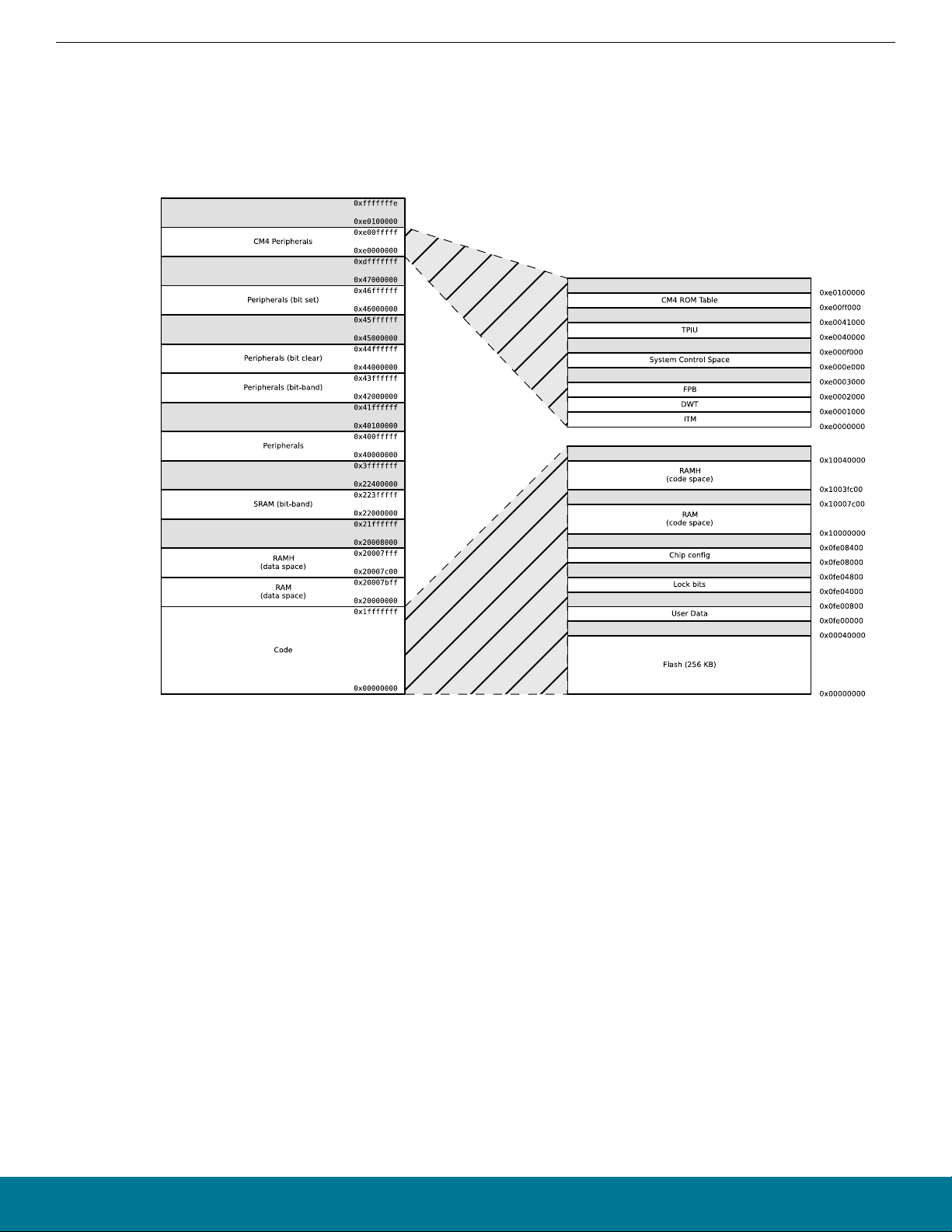
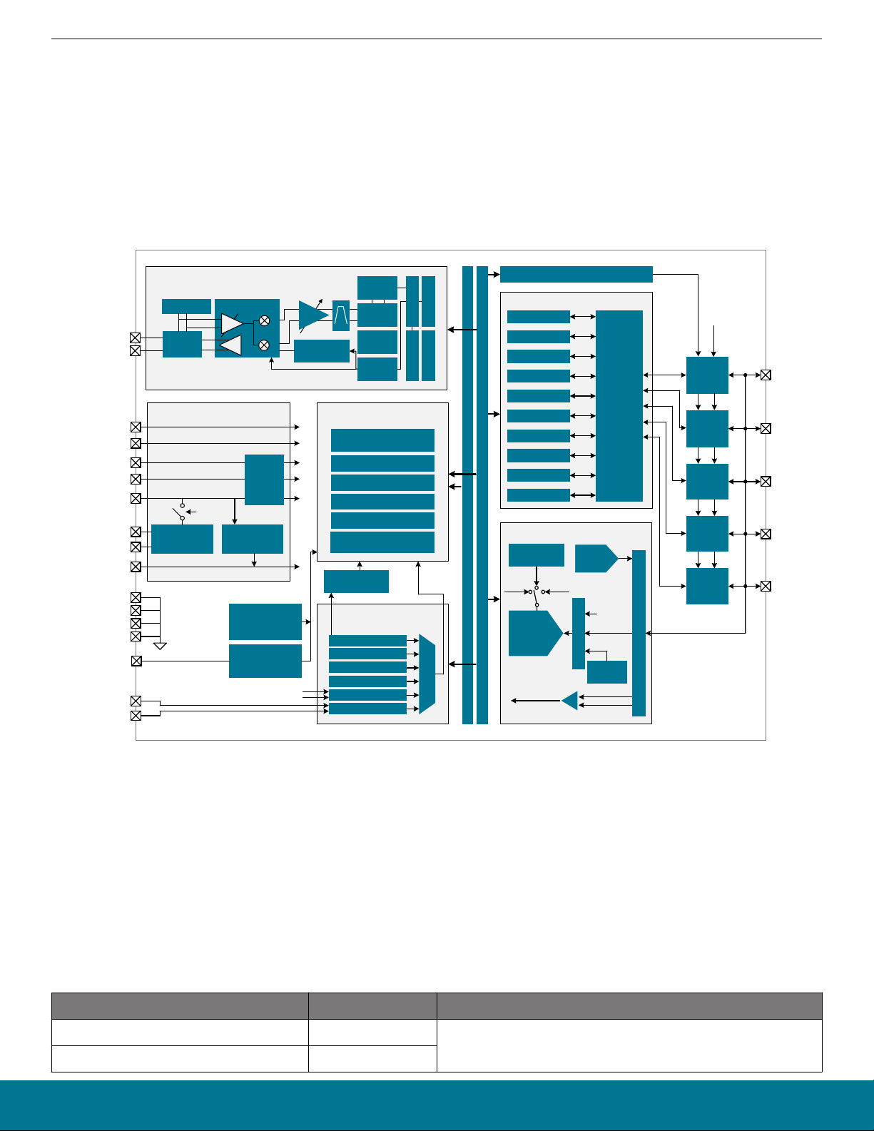
3.12 Memory Map
The BGM113 memory map is shown in the figures below.
BGM113 Blue Gecko Bluetooth® Smart Module Data Sheet
System Overview
Figure 3.2. BGM113 Memory Map — Core Peripherals and Code Space
silabs.com | Smart. Connected. Energy-friendly. Preliminary Rev. 0.93 | 9
BGM113 Blue Gecko Bluetooth® Smart Module Data Sheet
System Overview
Figure 3.3. BGM113 Memory Map — Peripherals
3.13 Configuration Summary
The features
of the BGM113 are a subset of the feature set described in the device reference manual. The table below describes de-
vice specific implementation of the features. Remaining modules support full configuration.
Table 3.2. Configuration Summary
Module Configuration Pin Connections
USART0 IrDA SmartCard US0_TX, US0_RX, US0_CLK, US0_CS
USART1
IrDA I2S SmartCard
US1_TX, US1_RX, US1_CLK, US1_CS
TIMER0 with DTI TIM0_CC[2:0], TIM0_CDTI[2:0]
TIMER1 TIM1_CC[3:0]
silabs.com | Smart. Connected. Energy-friendly. Preliminary Rev. 0.93 | 10

BGM113 Blue Gecko Bluetooth® Smart Module Data Sheet
Electrical Specifications
4. Electrical Specifications
4.1 Electrical Characteristics
All electrical parameters in all tables are specified under the following conditions, unless stated otherwise:
• Typical values are based on T
• Radio performance numbers are measured in conducted mode.
• Minimum and maximum values represent the worst conditions across supply voltage, process variation, and an operating temperature of -40 to +85 °C, unless stated otherwise.
Refer to Table 4.2 General Operating Conditions on page 12 for more details about operational supply and temperature limits.
4.1.1 Absolute Maximum Ratings
Stresses above those listed below may cause permanent damage to the device. This is a stress rating only and functional operation of
the devices at those or any other conditions above those indicated in the operation listings of this specification is not implied. Exposure
to maximum rating conditions for extended periods may affect device reliability.
Parameter Symbol Test Condition Min Typ Max Unit
=25 °C and VDD= 3.3 V, by production test and/or technology characterization.
AMB
Table 4.1. Absolute Maximum Ratings
Storage temperature range T
External main supply voltage V
External main supply voltage
STG
DDMAX
V
DDRAMPMAX
-50 — 150 °C
0 — 3.8 V
— — 1 V / μs
ramp rate
Voltage on any 5V tolerant
GPIO pin
1
V
DIGPIN
-0.3 — Min of 5.25
and IOVDD
V
+2
Voltage on non-5V tolerant
-0.3 — IOVDD+0.3 V
GPIO pins
Total current into VSS ground
I
VSSMAX
— — 200 mA
lines (sink)
Current per I/O pin (sink) I
IOMAX
— — 50 mA
Current per I/O pin (source) — — 50 mA
Current for all I/O pins (sink) I
Current for all I/O pins
IOALLMAX
— — 200 mA
— — 200 mA
(source)
Note:
1.
When a GPIO pin is routed to the analog module through the APORT, the maximum voltage = IOVDD.
silabs.com | Smart. Connected. Energy-friendly. Preliminary Rev. 0.93 | 11

BGM113 Blue Gecko Bluetooth® Smart Module Data Sheet
Electrical Specifications
4.1.2 Operating Conditions
4.1.2.1 General Operating Conditions
Table 4.2. General Operating Conditions
Parameter Symbol Test Condition Min Typ Max Unit
Operating temperature range T
VDD Operating supply voltage
HFCLK frequency f
OP
V
DD
CORE
-G temperature grade -40 25 85 °C
DCDC in regulation 2.4 3.3 3.8 V
DCDC in bypass 50mA load TBD 3.3 3.8 V
0 wait-states (MODE = WS0) — — 26 MHz
1 wait-states (MODE = WS1) — 38.4 38.4 MHz
silabs.com | Smart. Connected. Energy-friendly. Preliminary Rev. 0.93 | 12

BGM113 Blue Gecko Bluetooth® Smart Module Data Sheet
Electrical Specifications
4.1.3 Current Consumption
4.1.3.1 Current Consumption 1.85 V without DC-DC Converter
EMU_PWRCFG_PWRCG=NODCDC. EMU_DCDCCTRL_DCDCMODE=BYPASS. See 5.1 Power, Ground, Debug and UART.
Table 4.3. Current Consumption 1.85V without DC/DC
Parameter Symbol Test Condition Min Typ Max Unit
Current consumption in EM0
Active mode with radio disabled, All peripherals disabled
Current consumption in EM1
Sleep
mode with radio disa-
bled. All peripherals disabled
Current consumption in EM2
Deep Sleep
mode.
I
ACTIVE
I
EM1
I
EM2
38.4 MHz crystal, CPU running
— 128 — μA/MHz
while loop from flash
38 MHz HFRCO, CPU running
— 87 — μA/MHz
Prime from flash
38 MHz HFRCO, CPU running
— 103 — μA/MHz
while loop from flash
38 MHz HFRCO, CPU running
— 112 — μA/MHz
CoreMark from flash
26 MHz HFRCO, CPU running
— 105 — μA/MHz
while loop from flash
1 MHz HFRCO, CPU running
— 235 — μA/MHz
while loop from flash
38.4 MHz crystal —
61 — μA/MHz
38 MHz HFRCO — 35 — μA/MHz
26 MHz HFRCO — 37 — μA/MHz
1 MHz HFRCO — 167 — μA/MHz
Full RAM retention and RTCC
— 3.36 — μA
running from LFXO
4 kB RAM retention and RTCC
— 3.13 — μA
running from LFRCO
Current consumption in EM3
Stop mode
Current consumption in
EM4H Hibernate
mode
Current consumption in
EM4S Shutoff
mode
I
EM3
I
EM4
I
EM4S
Full RAM retention and CRYO-
— 2.84 — μA
TIMER running from ULFRCO
128 byte RAM retention, RTCC
—
1.08 — μA
running from LFXO
128 byte RAM retention, CRYO-
— 0.64 — μA
TIMER running from ULFRCO
128 byte RAM retention, no RTCC — 0.63 — μA
No RAM retention, no RTCC —
0.02 — μA
silabs.com | Smart. Connected. Energy-friendly. Preliminary Rev. 0.93 | 13

BGM113 Blue Gecko Bluetooth® Smart Module Data Sheet
Electrical Specifications
4.1.3.2 Current Consumption 3.3 V without DC-DC Converter
EMU_PWRCFG_PWRCG=NODCDC. EMU_DCDCCTRL_DCDCMODE=BYPASS. See 5.1 Power, Ground, Debug and UART.
Table 4.4. Current Consumption 3.3V without DC/DC
Parameter Symbol Test Condition Min Typ Max Unit
Current consumption in EM0
Active mode with radio disabled, All peripherals disabled
Current consumption in EM1
Sleep
mode with radio disa-
bled. All peripherals disabled
Current consumption in EM2
Deep Sleep
mode.
I
ACTIVE
I
EM1
I
EM2
38.4 MHz crystal, CPU running
— 129 — μA/MHz
while loop from flash
38 MHz HFRCO, CPU running
— 87 — μA/MHz
Prime from flash
38 MHz HFRCO, CPU running
— 103 — μA/MHz
while loop from flash
38 MHz HFRCO, CPU running
— 112 — μA/MHz
CoreMark from flash
26 MHz HFRCO, CPU running
— 105 — μA/MHz
while loop from flash
1 MHz HFRCO, CPU running
— 237 — μA/MHz
while loop from flash
38.4 MHz crystal —
61 — μA/MHz
38 MHz HFRCO — 35 — μA/MHz
26 MHz HFRCO — 37 — μA/MHz
1 MHz HFRCO — 170 — μA/MHz
Full RAM retention and RTCC
— 3.47 — μA
running from LFXO
4 kB RAM retention and RTCC
— 3.35 — μA
running from LFRCO
Current consumption in EM3
Stop mode
Current consumption in
EM4H Hibernate
mode
Current consumption in
EM4S Shutoff
mode
I
EM3
I
EM4
I
EM4S
Full RAM retention and CRYO-
— 2.92 — μA
TIMER running from ULFRCO
128 byte RAM retention, RTCC
—
1.13 — μA
running from LFXO
128 byte RAM retention, CRYO-
— 0.67 — μA
TIMER running from ULFRCO
128 byte RAM retention, no RTCC — 0.66 — μA
no RAM retention, no RTCC —
0.04 — μA
silabs.com | Smart. Connected. Energy-friendly. Preliminary Rev. 0.93 | 14

BGM113 Blue Gecko Bluetooth® Smart Module Data Sheet
Electrical Specifications
4.1.3.3 Current Consumption 3.3 V using DC-DC Converter
Table 4.5. Current Consumption 3.3V with DC/DC
Parameter Symbol Test Condition Min Typ Max Unit
Current consumption in EM0
Active mode with radio disabled. All peripherals disabled, DCDC in LowNoise
mode
Current consumption in EM1
Sleep
mode with radio disabled. All peripherals disabled, DCDC in LowPower
mode.
Current consumption in EM2
Deep Sleep
mode.
Current consumption in EM3
Stop mode
I
ACTIVE
I
EM1
I
EM2
I
EM3
38.4 MHz crystal, CPU running
— 87 — μA/MHz
while loop from flash.
38 MHz HFRCO, CPU running
— 63 — μA/MHz
Prime from flash
38 MHz HFRCO, CPU running
— 72 — μA/MHz
while loop from flash
38 MHz HFRCO, CPU running
— 78 — μA/MHz
CoreMark from flash
26 MHz HFRCO, CPU running
— 79 — μA/MHz
while loop from flash
38.4 MHz crystal —
39 — μA/MHz
38 MHz HFRCO — 23 — μA/MHz
26 MHz HFRCO — 25 — μA/MHz
1 MHz HFRCO — 142 — μA/MHz
Full RAM retention and RTCC
— 1.4 — μA
running from LFXO
4 kB RAM retention and RTCC
— 1.4 — μA
running from LFRCO
Full RAM retention and CRYO-
— 1.1 — μA
TIMER running from ULFRCO
Current consumption in
EM4H Hibernate
mode
Current consumption in
EM4S Shutoff
mode
I
EM4
I
EM4S
128 byte RAM retention, RTCC
—
0.9 — μA
running from LFXO
128 byte RAM retention, CRYO-
— 0.6 — μA
TIMER running from ULFRCO
128 byte RAM retention, no RTCC — 0.6 — μA
no RAM retention, no RTCC —
0.03 — μA
silabs.com | Smart. Connected. Energy-friendly. Preliminary Rev. 0.93 | 15

BGM113 Blue Gecko Bluetooth® Smart Module Data Sheet
Electrical Specifications
4.1.3.4 Current Consumption Using Radio
Table 4.6. Current Consumption Using Radio 3.3 V with DC-DC
Parameter Symbol Test Condition Min Typ Max Unit
Current consumption in receive mode, active packet
I
RX
1 Mbit/s, 2GFSK, F = 2.4 GHz,
— 8.7 — mA
Radio clock prescaled by 4
reception (MCU in EM1 @
38.4 MHz, peripheral clocks
disabled)
Current consumption in
transmit mode (MCU in EM1
@ 38.4 MHz, peripheral
clocks disabled)
RFSENSE current consump-
I
TX
I
RFSENSE
CW, 0 dBm, F = 2.4 GHz, Radio
— 8.8 — mA
clock prescaled by 3
CW, 3 dBm, F = 2.4 GHz — 17.6 — mA
— 51 — nA
tion
4.1.4 Wake up times
Table 4.7. Wake up times
Parameter Symbol Test Condition Min Typ Max Unit
Wake up from EM2 Deep
Sleep
Wakeup time from EM1
Sleep
t
EM2_WU
t
EM1_WU
Code execution from flash — 10.7 — μs
Code execution from RAM — 3 — μs
Executing from flash — 3 — AHB
Clocks
Executing from RAM — 3 — AHB
Wake up from EM3 Stop t
EM3_WU
Executing from flash — 10.7 — μs
Executing from RAM — 3 — μs
Wake up from EM4H Hiber-
1
nate
Wake up from EM4S Shut-
1
off
t
EM4H_WU
t
EM4S_WU
Executing from flash — 60 — μs
Note:
1.
Time from wakeup request until first instruction is executed. Wakeup results in device reset.
Clocks
— 290 — μs
silabs.com | Smart. Connected. Energy-friendly. Preliminary Rev. 0.93 | 16

BGM113 Blue Gecko Bluetooth® Smart Module Data Sheet
Electrical Specifications
4.1.5 Brown Out Detector
Table 4.8. Brown Out Detector
Parameter Symbol Test Condition Min Typ Max Unit
DVDDBOD threshold V
DVDD BOD hysteresis V
DVDD response time t
AVDD BOD threshold V
AVDD BOD hysteresis V
AVDD response time t
EM4 BOD threshold V
EM4 BOD hysteresis V
EM4 response time t
DVDDBOD
DVDDBOD_HYST
DVDDBOD_DELAY
AVDDBOD
AVDDBOD_HYST
AVDDBOD_DELAY
EM4DBOD
EM4BOD_HYST
EM4BOD_DELAY
4.1.6 Frequency Synthesizer Characteristics
Table 4.9. Frequency Synthesizer Characteristics
DVDD rising — — TBD V
DVDD falling TBD — — V
— 24 — mV
Supply drops at 0.1V/μs rate — 2.4 — μs
AVDD rising — — 1.85 V
AVDD falling TBD — — V
— 21 — mV
Supply drops at 0.1V/μs rate — 2.4 — μs
AVDD rising — — TBD V
AVDD falling TBD — — V
— 46 — mV
Supply drops at 0.1V/μs rate — 300 — μs
Parameter Symbol Test Condition Min Typ Max Unit
RF Synthesizer Frequency
F
RANGE_2400
2.4 GHz frequency range 2400 — 2483.5 MHz
range
LO tuning frequency resolution with 38.4
MHz crystal
Maximum frequency devia-
F
RES_2400
ΔF
MAX_2400
2400 - 2483.5 MHz —
—
— 73 Hz
— 1677 kHz
tion with 38.4 MHz crystal
silabs.com | Smart. Connected. Energy-friendly. Preliminary Rev. 0.93 | 17

4.1.7 2.4 GHz RF Transceiver Characteristics
BGM113 Blue Gecko Bluetooth® Smart Module Data Sheet
Electrical Specifications
4.1.7.1 RF Transmitter Characteristics for Bluetooth Smart
in the 2.4 GHz Band
Table 4.10. RF Transmitter Characteristics for Bluetooth Smart in the 2.4GHz Band
Parameter Symbol Test Condition Min Typ Max Unit
Transmit 6dB bandwidth TXBW — 740 — kHz
Power spectral density limit PSD
LIMIT
Per FCC part 15.247 — -6.5 — dBm/
3kHz
Per ETSI 300.328 at 10 dBm/1
— 10 — dBm
MHz
Occupied channel bandwidth
per ETSI EN300.328
In-band spurious emissions,
with allowed exceptions
Emissions of harmonics outof-band, per FCC part
15.247
Spurious emissions out-ofband, per FCC part 15.247,
excluding harmonics captured in SPUR
HARM,FCC
1
. Re-
OCP
SPUR
SPUR
SPUR
ETSI328
INB
HRM_FCC
OOB_FCC
99% BW at highest and lowest
— 1.1 — MHz
channels in band
At ±2 MHz — -39.8 — dBm
At ±3 MHz — -42.1 — dBm
2nd,3rd, 5, 6, 8, 9,10 harmonics;
— -47.3 — dBm
continuous transmission of modulated carrier
Above 2.483 GHz or below 2.4
— -47 — dBm
GHz; continuous transmission of
modulated carrier
2
stricted Bands
Spurious emissions out-ofband, per FCC part 15.247,
excluding harmonics captured in SPUR
HARM,FCC
.
Above 2.483 GHz or below 2.4
GHz; continuous transmission of
modulated carrier
— -26 — dBc
Non Restricted Bands
Spurious emissions out-ofband; per ETSI 300.328
SPUR
ETSI328
[2400-BW to 2400] MHz, [2483.5
to 2483.5+BW] MHz
[2400-2BW to 2400-BW] MHz,
— -16 — dBm
— -26 — dBm
[2483.5+BW to 2483.5+2BW]
MHz per ETSI 300.328
Spurious emissions per ETSI
EN300.440
SPUR
ETSI440
47-74 MHz,87.5-108 MHz,
174-230 MHz, 470-862 MHz
— -60 — dBm
25-1000 MHz — -42 — dBm
1-12 GHz — -36 — dBm
Note:
1.
Per Bluetooth Core_4.2, Section 3.2.2, exceptions are allowed in up to three bands of 1 MHz width, centered on a frequency
which is an integer multiple of 1 MHz. These exceptions shall have an absolute value of -20 dBm or less.
For 2480 Mhz, a maximum duty cycle of 20% is used to achieve this value.
2.
silabs.com | Smart. Connected. Energy-friendly. Preliminary Rev. 0.93 | 18

BGM113 Blue Gecko Bluetooth® Smart Module Data Sheet
Electrical Specifications
4.1.7.2 RF Receiver Characteristics for Bluetooth Smart in the 2.4 GHz Band
Table 4.11. RF Receiver Characteristics for Bluetooth Smart in the 2.4GHz Band
Parameter Symbol Test Condition Min Typ Max Unit
Max usable receiver input
level, 0.1% BER
SAT
Signal is reference signal1. Packet
length is 20 bytes.
Sensitivity, 0.1% BER SENS With dirty transmitter as defined in
Core_4.1
Signal to co-channel interferer, 0.1% BER
N+1 adjacent channel (1
MHz) selectivity, 0.1% BER,
with allowable exceptions.
C/I
C/I
CC
1+
Desired signal 3 dB above reference sensitivity
Interferer is reference signal at +1
MHz offset. Desired frequency
2402 MHz ≤ Fc ≤ 2480 MHz
Desired is reference signal at
-67
dBm
N-1 adjacent channel (1
MHz) selectivity, 0.1% BER,
with allowable exceptions.
C/I
1-
Interferer is reference signal at -1
MHz offset. Desired frequency
2402
MHz ≤ Fc ≤ 2480 MHz
Desired is reference signal at
-67 dBm
Alternate (2 MHz) selectivity,
0.1% BER, with allowable
exceptions. Desired is refer-
C/I
2
Interferer is reference signal at
± 2
MHz offset. Desired frequency
2402 MHz ≤ Fc ≤ 2480 MHz
ence signal at -67 dBm
Alternate (3 MHz) selectivity,
0.1% BER, with allowable
exceptions. Desired is refer-
C/I
3
Interferer is reference signal at
±3
MHz offset. Desired frequency
2404 MHz ≤ Fc ≤ 2480 MHz
ence signal at -67 dBm
— 10 — dBm
— -91.8 — dBm
— 8.3 — dB
— -3 — dB
— -0.5 — dB
— -43 — dB
— -46.7 — dB
Selectivity to image frequency, 0.1% BER. Desired is reference signal at -67
dBm
Selectivity to image frequency +1
MHz, 0.1% BER. De-
sired is reference signal at
-67 dBm
Blocking, 0.1% BER, Desired
is reference signal at -67
dBm. Interferer is CW in
OOB range.
Intermodulation performance
per Core_4.1, Vol 6 Section
4.4 (n = 3 alternative), 0.1%
BER.
C/I
IM
Interferer is reference signal at image frequency with 1 MHz precision
C/I
IM+1
Interferer is reference signal at image frequency +1 MHz with 1
MHz precision
BLOCK
OOB
Interferer frequency 30 MHz ≤ f ≤
2000 MHz
Interferer frequency 2003 MHz ≤ f
≤ 2399 MHz
Interferer frequency 2484 MHz ≤ f
≤ 2997 MHz
Interferer frequency 3 GHz ≤ f ≤
12.75
GHz
IM Desired is reference signal at 6dB
above reference sensitivity level.
Interferer 1 is CW at level IM
BLE
Interferer 2 is reference signal at
IM
.
BLE
— -38.7 — dB
— -48.2 — dB
—
-27 — dBm
— -32 — dBm
— -32 — dBm
— -27 — dBm
— -33 — dBm
.
silabs.com | Smart. Connected. Energy-friendly. Preliminary Rev. 0.93 | 19

BGM113 Blue Gecko Bluetooth® Smart Module Data Sheet
Electrical Specifications
Parameter Symbol Test Condition Min Typ Max Unit
Upper limit of input power
RSSI
MAX
range over which RSSI resolution is maintained
Lower limit of input power
RSSI
MIN
range over which RSSI resolution is maintained
RSSI resolution RSSI
RES
Over RSSI
Note:
1.
Reference signal is defined 2GFSK at -67
dBm, Modulation index = 0.5, BT = 0.5, Bit rate = 1 Mbps, desired data = PRBS9;
interferer data = PRBS15; frequency accuracy better than 1 ppm
MIN
to RSSI
MAX
4 — — dBm
— — -101 dBm
— — 0.5 dB
silabs.com | Smart. Connected. Energy-friendly. Preliminary Rev. 0.93 | 20

BGM113 Blue Gecko Bluetooth® Smart Module Data Sheet
Electrical Specifications
4.1.8 Oscillators
4.1.8.1 LFXO
Table 4.12. LFXO
Parameter Symbol Test Condition Min Typ Max Unit
Crystal frequency f
Current consumption after
LFXO
I
LFXO
GAIN1, AGC
1
— 32.768 — kHz
— 273 — nA
startup
Start- up time t
LFXO
GAIN
1
— 308 — ms
Note:
1. In CMU_LFXOCTRL register
4.1.8.2 HFXO
Table 4.13. HFXO
Parameter Symbol Test Condition Min Typ Max Unit
Crystal Frequency f
Startup time t
Frequency Tolerance for the
HFXO
HFXO
FT
HFXO
38.4 MHz: BOOST1 = 2
— 300 — μs
38.4 MHz -25 — 25 ppm
38.4 MHz
crystal
Note:
1. In CMU_HFXOCTRL register
4.1.8.3 LFRCO
Table 4.14. LFRCO
Parameter Symbol Test Condition Min Typ Max Unit
Oscillation frequency f
LFRCO
ENVREF = 1 in
TBD 32.768 TBD kHz
CMU_LFRCOCTRL
ENVREF = 0 in
TBD 32.768 TBD kHz
CMU_LFRCOCTRL
Startup time t
Current consumption
1
LFRCO
I
LFRCO
ENVREF = 1 in
— 500 — μs
— 342 — nA
CMU_LFRCOCTRL
ENVREF = 0 in
— 494 — nA
CMU_LFRCOCTRL
Note:
1.
Block is supplied by AVDD if ANASW = 0, or DVDD if ANASW=1 in EMU_PWRCTRL register
silabs.com | Smart. Connected. Energy-friendly. Preliminary Rev. 0.93 | 21
 Loading...