

Silicon Laboratories Finland APX4 Datasheet

APX4 – WIRELESS SYSTEM-ON-MODULE
DATA SHEET
Tuesday, 23 July 2013
Version 1.01

Copyright © 2000-2013 Bluegiga Technologies
All rights reserved.
Bluegiga Technologies assumes no responsibility for any errors which may appear in this manual.
Furthermore, Bluegiga Technologies reserves the right to alter the hardware, software, and/or specifications
detailed here at any time without notice and does not make any commitment to update the information
contained here. Bluegiga’s products are not authorized for use as critical components in life support devices
or systems.
The WRAP, Bluegiga Access Server, Access Point and iWRAP are registered trademarks of Bluegiga
Technologies.
The Bluetooth trademark is owned by the Bluetooth SIG Inc., USA and is licensed to Bluegiga Technologies.
All other trademarks listed herein are owned by their respective owners.
Bluegiga Technologies Oy

VERSION HISTORY
Version
Comment
0.1
First draft
0.2
Defined screws and attachment to motherboard
0.3.1
Some small fixes and additions
0.3
TBDs defined
0.4
Review
0.4.1
Small fix to part number clarification
0.4.2
Updated document name, product description and contact information
0.4.3
Added Bluetooth RF specifications
0.5
Clarified pins etc.
0.6
Fixed layout. Removed software version from part number.
0.7
Styles updated and fixed
Added notes about missing information
0.8
Added Mouser part number for the SO-DIMM receptacle
0.9
Chapter 6.5.1 removed
1.0
Added FCC/IC texts, removed battery related texts
1.01
Typos
Bluegiga Technologies Oy

TABLE OF CONTENTS
1 Ordering Information......................................................................................................................................7
1.1 Part number decoder .............................................................................................................................7
2 APx4 pin descriptions ....................................................................................................................................8
2.1 Receptacle ............................................................................................................................................8
2.2 Power contacts on the left side .............................................................................................................8
2.3 Debug UART on the right side ..............................................................................................................8
2.4 SO-DIMM connection pin descriptions ..................................................................................................9
3 Power subsystem ....................................................................................................................................... 22
3.1 PSWITCH_OUT pin 14 ...................................................................................................................... 23
3.2 RESETN ............................................................................................................................................. 23
4 Processor subsystem ................................................................................................................................. 24
4.1 Bootmodes ......................................................................................................................................... 24
5 Wireless interfaces ..................................................................................................................................... 25
5.1 Bluetooth ............................................................................................................................................ 25
5.1.1 Bluetooth GPIOs ........................................................................................................................... 25
5.1.2 Bluetooth Audio interface .............................................................................................................. 25
5.1.3 Bluetooth PCM slots and formats.................................................................................................. 26
5.1.4 Bluetooth I2S interface .................................................................................................................. 26
5.2 Wi-Fi ................................................................................................................................................... 27
6 Peripheral interfaces................................................................................................................................... 28
6.1 Ethernet .............................................................................................................................................. 28
6.2 USB .................................................................................................................................................... 29
6.3 I2C ...................................................................................................................................................... 29
6.4 PWM outputs ...................................................................................................................................... 30
6.5 SDIO / SPI / MMC .............................................................................................................................. 31
6.6 UARTs ................................................................................................................................................ 32
6.6.1 UART 0 .......................................................................................................................................... 32
6.6.2 UART 2 .......................................................................................................................................... 32
6.6.3 UART 3 .......................................................................................................................................... 32
6.6.4 UART 4 .......................................................................................................................................... 33
6.6.5 Debug UART ................................................................................................................................. 33
6.7 CAN .................................................................................................................................................... 34
6.8 Processor Audio ................................................................................................................................. 34
6.9 LCD .................................................................................................................................................... 35
6.10 LRADC0-6 (Touch interface) .............................................................................................................. 36
6.11 HSADC (High-Speed ADC) ................................................................................................................ 37
Bluegiga Technologies Oy

6.12 JTAG .................................................................................................................................................. 37
7 Electrical Characteristics ............................................................................................................................ 39
7.1 Absolute Maximum Ratings................................................................................................................ 39
7.2 Recommended Operating Conditions ................................................................................................ 39
7.3 Power Consumption ........................................................................................................................... 40
8 RF Characteristics ...................................................................................................................................... 41
9 Physical Dimensions .................................................................................................................................. 43
10 Attachment to motherboard ................................................................................................................ 44
11 Layout Guidelines ............................................................................................................................... 45
11.1 Internal antenna: Optimal module placement .................................................................................... 45
11.2 External antenna ................................................................................................................................ 45
11.3 Thermal Considerations ..................................................................................................................... 45
11.4 EMC Considerations for Motherboard ................................................................................................ 45
12 Certifications ....................................................................................................................................... 47
12.1 CE ....................................................................................................................................................... 47
12.2 FCC .................................................................................................................................................... 47
12.3 IC ........................................................................................................................................................ 48
12.4 IC ........................................................................................................................................................ 49
12.5 MIC, formerly TELEC ......................................................................................................................... 51
12.6 Qualified Antenna Types for APx4-E ................................................................................................. 51
13 Contact Information ............................................................................................................................ 52
Bluegiga Technologies Oy
DESCRIPTION
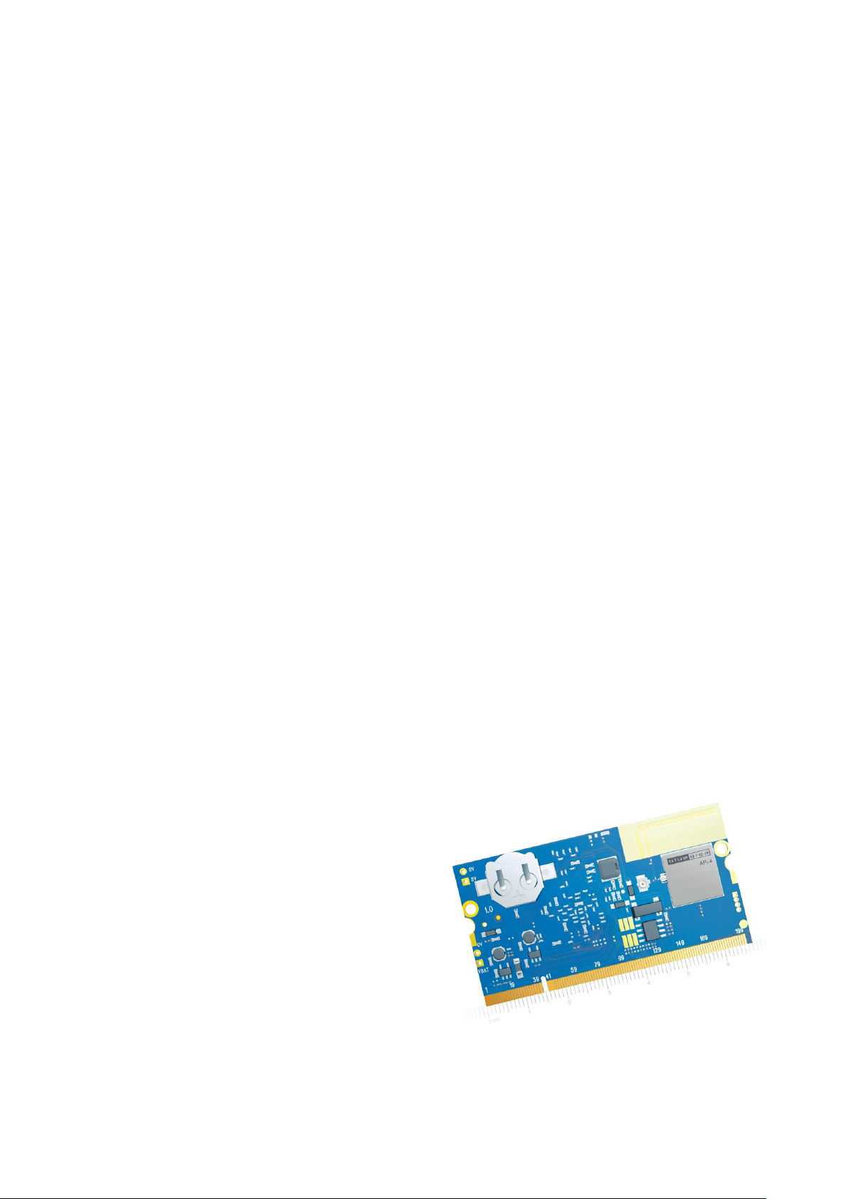
The Bluegiga APx4 is a small form factor, low
power system-on-module that includes the
latest wireless connectivity standards: 802.11
b/g/n and Bluetooth 4.0. APx4 is based on
Freescale's i.MX28 processor family and runs
an embedded Linux operating system based on
the Yocto ProjectTM. In addition to integrating
the 454MHz ARM9 processor, the wireless
connectivity technologies, Linux operating
system the APx4 also includes with several built
in applications, such as the 802.11
and Bluetooth 4.0 stacks, Continua
v.1.5 compliant IEEE manager and many more.
This combination provides an ideal platform for
designing multi-radio wireless gateways that
enables fast time-to-market and minimum R&D
risks.
The Bluegiga APx4 software can be easily
extended or tailored customizing the Linux
operating system with applications. The
motherboards for the APx4 can be easily
extended to include almost anything from 3G
modems to Ethernet and audio interfaces to
and touch screen displays.
The Bluegiga APx4 is an ideal product for
applications requiring wireless or wired
connectivity technologies and the processing
power of the ARM9 processor, such as health
and fitness gateways, building and home
automation gateways, M2M, point-of-sale and
industrial connectivity.
KEY FEATURES
APx4 is a computing platform:
454MHz ARM9 core (Freescale
i.MX28)
64MB RAM
128MB Flash
Real Time Clock
Linux operating system
SO-DIMM form factor
A connectivity platform:
Bluetooth 4.0 dual-mode radio
2.4GHz 802.11 b/g/n radio
Wi-Fi Access Point mode
10/100 Ethernet
USB 2.0 High Speed
With many extension options:
Up to 800 x 480, 24bit display
Resistive touch screen
MMC/SDIO
Multiple SPI, UART and I²C
I²S
PWM, GPIO and AIO
Linux operating system:
Based on the Yocto Project(TM)
Thousands of open source software
packets available
APPLICATIONS:
Health gateways
M2M connectivity
Fitness gateways
Home and building automation
Point-of-sale gateways
People and asset tracking
Qualifications:
Bluetooth
CE
FCC and IC
Figure 1: Physical outlook
Bluegiga Technologies Oy
Product code
CPU and memories
Connectivity
Antenna
Temperature
range
APX4-367CC-A
i.MX283
64MB DDR2
128MB Flash
Bluetooth + Wi-Fi
Internal
antenna
-10 – 50°C
APX 4 – 3 6 7 C C – A
Product category
APX
Product generation
4
Processor
3: i.MX283
Memory
6: 64MB
Flash
7: 128MB
Connectivity
C: Bluetooth and Wi-Fi
Temperature
C: Commercial
I: Industrial (contact sales@bluegiga.com)
Antenna
A: Internal antenna
E: External antenna
1 Ordering Information
1.1 Part number decoder
Note: Not all variants are available. Minimum order quantities and lead times may apply for special variants.
Please contact Bluegiga Technologies Oy for more information.
Bluegiga Technologies Oy
Page 7 of 52
Name
Function
GND
Ground
VIN
+5V input
GND
Ground
VBATTERY
Battery positive input/output
Name
Function
3V3
3.3V output (for current limits, see Table 50)
PWM1/DUART TxD
Debug UART data transmit, logic level 3.3V
PWM0/DUART RxD
Debug UART data receive, logic level 3.3V
GND
Ground
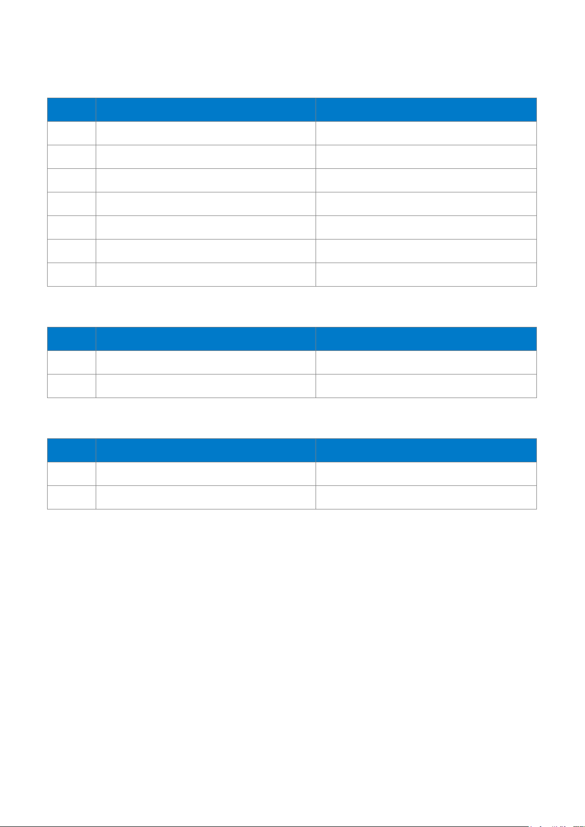
2 APx4 pin descriptions
The APX4 connector uses a standard DDR1 SO-DIMM connector with 2.5V keying.
Odd numbered pins are located on top layer
Even numbered pins are located on bottom layer
There is a ½ pitch (0.3mm) offset from top layer pins to bottom layer pins.
Note that most receptacles also have 0.3mm offset from odd pins to even pins.
2.1 Receptacle
Suitable receptacles are available from multiple vendors. For example TE Connectivity’s part number
1473005-1, Mouser part number: 571-1473005-1 and Digi-Key’s part number: A99605-ND.
PCB footprint and schematic symbol for the mentioned part number will be available for download
from Techforum in Mentor Graphics’ PADS format.
2.2 Power contacts on the left side
In addition to the 200 pins/finger contacts there are two pairs of plated through holes on the left side of the
module which can be used for powering the module stand-alone (not assembled on any motherboard). The
pitch between the holes is 2.54mm. Leave the holes unconnected if the module is assembled on a
motherboard.
Table 1: Power supply pins
2.3 Debug UART on the right side
On the right side there are four plated through holes for PWM or debug port stand-alone (not assembled on
any motherboard). The vertical distance between the holes is 1.27mm:
Table 2: Debug UART pins
Bluegiga Technologies Oy
Page 8 of 52

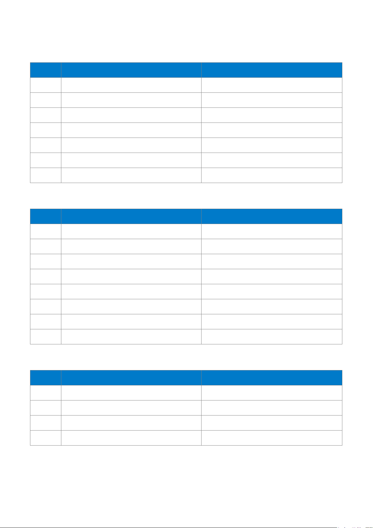
Pin#
Default function
Net name
Note
1
5V input
VIN 2
5V input
VIN 3
5V input
VIN 4
5V input
VIN 5
Battery input/output
VBATTERY
6 Battery input/output
VBATTERY
7 Battery input/output
VBATTERY
8 Bootmode
BOOTMODE
9
3.3V output
3V3
Pins 9-10 may source up to
200mA combined.
10
3.3V output
3V3
Pins 9-10 may source up to
200mA combined.
11
3.3V output
3V3
Pins 9-10 may source up to
200mA combined.
12
3.3V output
3V3
Pins 9-10 may source up to
200mA combined.
13
RTC battery
VBACKUP
14
PS switch
PSWITCH_OUT
15
NC
NC 16
NC
NC 17
Reset in - Master reset
RESETN
18
Ground
GND
2.4 SO-DIMM connection pin descriptions
Note: Signals/nets marked with a star (*) are not present on standard version
Table 3: Main power pins
Bluegiga Technologies Oy
Page 9 of 52
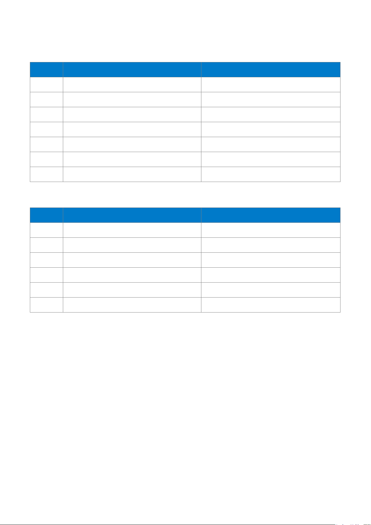
Pin#
Default function
Net name
19
Ethernet TX -
ETN_TXN
20
GND
GND
21
Ethernet TX +
ETN_TXP
22
3.3V output
3V3
23
Ethernet RX -
ETN_RXN
24
Ethernet LED
ETN_LED1N*
25
Ethernet RX +
ETN_RXP
26
GND
GND
Pin#
Default function
Net name
27
USB External VBUS enable
SPDIF*
28 NC
29
USB D-
USB1DM
30 NC
31
USB D+
USB1DP
32
Ground
GND
Table 4: Ethernet
* See 6.1 for detailed function.
Table 5: USB Host
Bluegiga Technologies Oy
Page 10 of 52
Pin#
Default function
Net name
33
USB OTG id
USB0_ID
34 NC
35
USB D-
USB0DM
36 NC
37
USB D+
USB0DP
38 NC
39
Ground
GND
Pin#
Default function
Net name
40
I2C Data
I2C0_SDA
41
I2C Clock
I2C0_SCL
Pin#
Default function
Net name
42
PWM (Backlight)
PWM4
43
Status led
PWM3
Table 6: USB On-the-go
Table 7: I2C 0
Table 8: Dedicated PWMs
Bluegiga Technologies Oy
Page 11 of 52
Pin#
Default function
Net name
44
Slave select 1
SDIO_DAT1_OUT*
45
Slave select 2
SDIO_DAT2_OUT*
46
Command - Master out, slave in
SDIO_CMD_OUT*
47
Data 0, Master in, slave out
SDIO_DAT0_OUT*
48
Clock
SDIO_CLK_OUT*
49
Ready - Slave select 0
SDIO_DAT3_OUT*
50
Ground
GND
Pin#
Default function
Net name
51
Card detect
SSP0_DETECT
52
Data 0
SSP0_DATA0
53
Data 1
SSP0_DATA1
54
Data 2
SSP0_DATA2
55
Data 3
SSP0_DATA3
56
Command
SSP0_CMD
57
Clock
SSP0_SCK
58
Ground
GND
Pin#
Default function
Net name
59
UART transmit
AUART0_TX
60
UART receive
AUART0_RX
61
UART clear-to-send
AUART0_CTS
62
UART request-to-send
AUART0_RTS
Table 9: SSP2 – SDIO/MMC/SPI
Table 10: SSP0 – SDIO/MMC/SPI
Table 11: UART 0
Bluegiga Technologies Oy
Page 12 of 52

Pin#
Default function
Net name
63
UART transmit
SSP2_MOSI
64
UART receive
SSP2_SCK
65 NC
66 NC
Pin#
Default function
Net name
67
UART transmit
SSP2_SS0
68
UART receive
SSP2_MISO
69 NC
70 NC
71
Ground
GND
Pin#
Default function
Net name
72
Bluetooth GPIO
BT_PIO7
73
Bluetooth GPIO
BT_PIO8
74
Bluetooth GPIO
BT_PIO9
75
Bluetooth GPIO
BT_PIO25
Table 12: UART 2
Table 13: UART 3
Table 14: Bluetooth GPIO
Bluegiga Technologies Oy
Page 13 of 52
Pin#
Default function
Net name
76
CAN 0 transmit
GPMI_RDY2*
77
Ground
GND
78
CAN 1 transmit
GPMI_CE2N*
79
CAN 1 receive
GPMI_CE3*
80
Ground
GND
81
CAN 0 receive
GPMI_RDY3*
82
Ground
GND
Pin#
Default function
Net name
83
MCLK
SAIF0_MCLK
84
Data line 1
SAIF1_SDATA0
85
Data line 0
SAIF0_SDATA0
86
Bit clock
SAIF0_BITCLK
87
Left/Right clock
SAIF0_LRCLK
88
GND
GND
Table 15: CAN
Table 16: Primary audio / UART 4
Bluegiga Technologies Oy
Page 14 of 52

Pin#
Default function
Net name
89 NC
90 NC
91 NC
92 NC
93 NC
94
Ground
GND
95 NC
96 NC
97 NC
98 NC
99 NC
100 NC
Table 17: Reserved group 1
Bluegiga Technologies Oy
Page 15 of 52

Pin#
Default function
Net name
101 NC
102
Ground
GND
103 NC
104 NC
105 NC
106 NC
107
1.4V output*
1V4_CPU
108
1.8V output*
1V8
109
4.2V output*
4V2_CPU
110 NC
111 GND
112 NC
113 NC
114 NC
115 NC
116
Ground
GND
Table 18: Reserved group 2
*Important: Pins 107-109 are only meant for manufacturing test. Please leave unconnected. Do not pull any
current from these outputs. Doing so may create a black hole in the universe.
Bluegiga Technologies Oy
Page 16 of 52
 Loading...