


Silicon Laboratories Z-WAVE 700 Integration Manual
INSTRUCTION: Z-Wave 700 Integration Guide
INS14487-3 | 2/2019 1
INTEGRATION GUIDE FOR SILICON LABS ZENGECKO Z-WAVE® DEVICES
Type
QFN32
SoC
5mm x 5mm
LGA64
SiP
9mm x 9mm
Chip
EFR32ZG14
Module
ZGM130S
The purpose of this document is to provide an implementation guide for integrating Z-Wave 700 devices into product designs.
It is intended for product design engineers who aim for a fast integration of Z-Wave 700 devices.
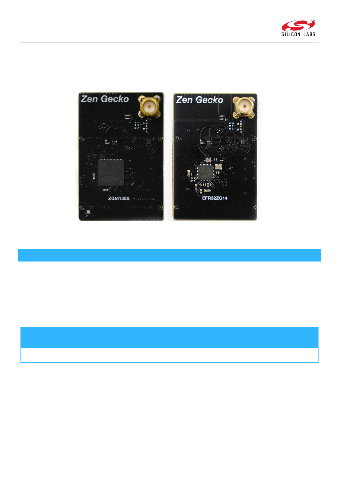
1 OV ERVI EW
The Z-Wave 700 device portfolio is shown in Table 1.1. The EFR32ZG14 gateway SoC exposes the Z-Wave serial API via UART and
is dedicated to gateway applications. The ZGM130S SiP module combines a general-purpose SoC, crystal, supply decoupling
components, and RF matching components into a single small-footprint module requiring only two decoupling capacitors. The
ZGM130S is targeted at end device applications and, with its built-in ARM M4 core and ultra-low power consumption, it is perfect
for making single chip sensors and other end devices that require advanced processing and low power consumption.
Table 1.1: Z-Wave 700 device portfolio
The applicable modules are clearly stated at the beginning of each of the following sections.

Instruction: Z-Wave Z-Wave 700 Integration Guide
2 INS14487-3 | 2/2019
2 CON TENT
1 OVERVIEW.........................................................................................................................................................................1
3 PROGRAMMING AND DEBUGGING INTERFACE ..................................................................................................................3
3.1 PROGRAMMING INTERFACE OVERVIEW .........................................................................................................................................4
4 CALIBRATION.....................................................................................................................................................................4
4.1 CRYSTAL .................................................................................................................................................................................4
5 RF VERIFICATION TOOL......................................................................................................................................................4
6 COMPONENT SPECIFICATIONS ...........................................................................................................................................4
6.1 SAW FILTER............................................................................................................................................................................4
6.1.1 Recommended Components for GSM/LTE gateways ..................................................................................................6
6.1.2 OPTIONAL Components for GSM/LTE gateways..........................................................................................................6
6.2 CRYSTAL .................................................................................................................................................................................6
6.2.1 Recommended Components ........................................................................................................................................7
7 SUPPLY FILTER ...................................................................................................................................................................7
8 MATCHING CIRCUIT ...........................................................................................................................................................7
8.1 SOC TO RF LINE MATCHING ........................................................................................................................................................7
8.1.1 Mandatory Components..............................................................................................................................................8
8.2 RF LINE TO ANTENNA MATCHING .................................................................................................................................................8
8.3 MEASUREMENT SETUP ..............................................................................................................................................................9
9 PCB IMPLEMENTATION....................................................................................................................................................10
9.1 PLACEMENT ..........................................................................................................................................................................10
9.2 STACK-UP .............................................................................................................................................................................10
9.3 POWER ROUTING ...................................................................................................................................................................10
9.4 DECOUPLING .........................................................................................................................................................................11
9.4.1 For ZGM130S end device SiP......................................................................................................................................11
9.4.2 For EFR32ZG14 gateway SoC.....................................................................................................................................11
9.5 RF TRACE .............................................................................................................................................................................12
9.6 IC GROUNDING......................................................................................................................................................................13
10 ANTENNA DESIGN ........................................................................................................................................................13
11 ESD ..............................................................................................................................................................................13
12 ABBREVIATIONS...........................................................................................................................................................14
13 REVISION HISTORY .......................................................................................................................................................16
14 REFERENCES.................................................................................................................................................................17
Instruction: Z-Wave 700 Integration Guide
INS14487-3 | 2/2019 3
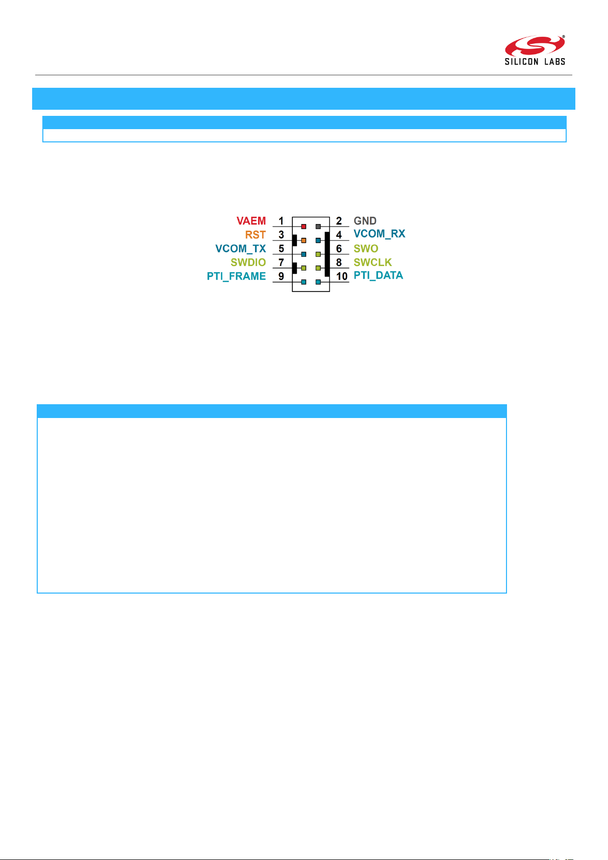
3 PRO GRAM MING AND DEB UGGI NG I NTERFACE
EFR32ZG14
ZGM130S
Applicable
Applicable
Figure 3.1: Silicon Labs Mini Simplicity Header
Pin Name
Pin Location
Type
Function
GND2S
Common ground between the programmer and Z-Wave 700
device
VAEM
1STarget voltage on the debugged application. Supplied and
monitored by the AEM when power selection switch is in the
"AEM" position.
RST3O
Driven low by the programmer to place the Z-Wave 700 device in
a reset state
VCOM_TX
5IReceive UART serial data from Z-Wave 700 device
VCOM_RX
4OTransmit UART serial data to Z-Wave 700 device
SWO
6ISerial Wire Output
SWDIO
7
I/O
Serial Wire Data
SWCLK
8OSerial Wire Clock
PTI_FRAME
9IPacket Trace Frame Signal
PTI_DATA
10IPacket Trace Data Signal
A programming interface is mandatory if In-System Programming of a Z-Wave 700 device is required, i.e., programming while
soldered onto the product PCB. To design in a footprint for the Mini Simplicity header, Silicon Labs recommends using a small 10pin 1.27 mm SMD header for both programming and debugging of chips from the Silicon Labs Gecko family.
If a connector is used, the Samtec FTSH-105-01-F-DH surface mounted or Harwin M50-3500542 through-hole male connector is
recommended and can be directly used with the BRD8010A STK/WSTK Debug Adapter. The functionality of the pins from the
programmer’s perspective is shown in Table 3.1. Refer to [1] for programming instructions.
Table 3.1: Z-Wave 700 Mini Simplicity Header Pin Functionality
Instruction: Z-Wave Z-Wave 700 Integration Guide
4 INS14487-3 | 2/2019
3.1 PRO GRAM MING INT ERFA CE O VERV IEW
EFR32ZG14
ZGM130S
SWD programming
XXBoot Loader UART programming
X
X
EFR32ZG14
ZGM130S
Applicable
N/A
EFR32ZG14
ZGM130S
Applicable
Applicable
EFR32ZG14
ZGM130S
Applicable
NA
The table below shows which interfaces can be used to program the flash memory of the various Z-Wave 700 products:
Table 3.2: Available programming interfaces
4 CAL IBRA TION
It is mandatory to calibrate the crystal in EFR32ZG14 Z-Wave 700 devices during product development to make sure that the mean
value of the crystal frequency is correct. Refer to [4] for calibration instructions. Furthermore, for best possible performance, it is
recommended that calibration be performed during production to minimize the spread in crystal frequency. All ZGM130S Z-Wave
700 devices are calibrated during production and therefore do not need any further crystal calibration.
4.1 CRY STAL
It is recommended to calibrate the crystal frequency for the gateway devices to ensure minimum error of the radio carrier
frequency.
5 RF VERI FICA TION TOO L
The RailTest tool can be used to verify the RF performance of a device without the overhead of the Z-Wave protocol. The same RF
PHY present in the Z-Wave protocol is used. The tool is suitable when investigating RF performance and performing RF regulatory
tests. To use the tool, it is required that the chip is programmable and the UART0 is connected to a terminal over RS-232 or
through the WSTK. For a comprehensive user’s manual for the RailTest tool, refer to [2] and [3].
As the RF PHY can be updated for new software releases, it is important to compile a RailTest version based on the same software
release that will be used in the final product.
6 COM PONE NT S PECI FICA TION S
6.1 SAW FIL TER
It is recommended that a SAW filter is used in Z-Wave 700 gateway designs also containing GSM or LTE transceivers operating in
the subGHz band. A SAW filter attenuates unwanted radio emissions and improves the receiver blocking performance. Three
Instruction: Z-Wave 700 Integration Guide
INS14487-3 | 2/2019 5
regions are defined to cover the global Z-Wave frequency range. The SAW filter specifications described in Table 6.1, Table 6.2,
Frequency Range
Unit
Minimum
Typical
Maximum
Operating temperature
-
◦
C
-30-+85
Insertion loss
865.0 to 870.1MHz
dB
--3.5
Amplitude ripple
865.0 to 870.1MHz
dB
--2.0
Relative attenuation
0.1 to 800.0MHz
dB
40--
805 to 830MHz
dB
35--
835 to 855MHz
dB
---
860 to 862MHz
dB
---
890 to 1000MHz
dB
40--
1005 to 2000MHz
dB
30--
2005 to 3000MHz
dB
30--
3005 to 4000MHz
dB
30--
4005 to 6000MHz
dB
---
In / out impedance
-Ω-50-
Frequency Range
Unit
Minimum
Typical
Maximum
Operating temperature
-
◦
C
-30-+85
Insertion loss
908.2 to 916.3MHz
dB
--2.5
Amplitude ripple
908.2 to 916.3MHz
dB
--1.5
Relative attenuation
720 to 800MHz
dB
45--
805 to 840MHz
dB
---
845 to 870MHz
dB
40--
870 to 895MHz
dB
---
940 to 1000MHz
dB
9--
1005 to 2000MHz
dB
9--
2005 to 3000MHz
dB
17--
3005 to 4000MHz
dB
---
4005 to 6000MHz
dB
---
In / out impedance
-Ω-50-
Frequency Range
Unit
Minimum
Typical
Maximum
Operating temperature
-
◦
C
-30-+85
Insertion loss
919.5 to 926.5MHz
dB
--3.2
Amplitude ripple
919.5 to 926.5MHz
dB
--1.0
Relative attenuation
40 to 870MHz
dB
40--
875 to 885MHz
dB
35--
890 to 905MHz
dB
20--
945 to 955MHz
dB
20--
960 to 1000MHz
dB
20--
1005 to 1500MHz
dB
40--
1505 to 3000MHz
dB
20--
3005 to 4000MHz
dB
---
4005 to 6000MHz
dB
---
In / out impedance
-Ω-50-
and Table 6.3 are recommended for new designs.
Table 6.1: Region E
Table 6.2: Region U
Table 6.3: Region H
Instruction: Z-Wave Z-Wave 700 Integration Guide
6 INS14487-3 | 2/2019
6.1 .1 REC OMME NDED COM PONE NTS FOR GSM/LTE G ATEW AYS
Region
Distributor
Component Number
Note
E
ACTE A/S, www.acte.dk, salessupport@acte.dk
SF4000-868-07-SX
Preferred
U
ACTE A/S, www.acte.dk, salessupport@acte.dk
SF4000-914-06-SX
Preferred
H
ACTE A/S, www.acte.dk, salessupport@acte.dk
SF1256-923-02
Preferred
Region
Distributor
Component Number
Note
E
ACTE A/S, www.acte.dk, salessupport@acte.dk
SF4000-869-14-SX
Improved LTE rejection
EFR32ZG14
ZGM130S
Applicable
NA
Parameter
Symbol
Min
Typ
Max
Unit
Crystal frequency
fHFXO
—39—
MHz
Supported crystal equivalent series resistance (ESR)
ESRHFXO_39M
——60
Ω
Supported range of crystal load capacitance 1
CHFXO_CL
6—12
pF
Initial frequency tolerance for the crystal
FTHFXO
-10 10
ppm
Temperatur tolerance for the crystal
FTempHFXO
-40°C - 85°C
-12 12
ppm
Aging
FAge
-3 3
ppm/5yr
Combined tolerance for the crystal
FTtotalHFXO
-25—25
ppm/5yr
Table 6.4: SAW filters
6.1 .2 OPT IONA L CO MPON ENTS FOR GSM /LTE GATE WAYS
Table 6.5: LTE improved SAW filters
6.2 CRY STAL
The crystal is part of the oscillator that generates the reference frequency for the digital system clock and RF carrier. It is a critical
component of a Z-Wave 700 device. Further, it is mandatory to calibrate the crystal for gateway designs. Refer to section 4 for
more information.
The EFR32ZG14 has internal crystal capacitors and does not need any external circuitry apart from the crystal itself.
The ZGM130S has an integrated crystal and is calibrated at the time of production.
Table 6.6: Crystal specification for Z-Wave 700 devices