

Page 1
UG384: WGM160P Hardware Design
User’s Guide
The purpose of this guide is to help users design WiFi applications using the WGM160P.
This guide includes information for schematics and layout. Some options available with
WGM160P hardware are not available with all software architectures, so the pin features
versus software are detailed.
KEY FEATURES
• Schematic guidelines
•
Package information
• Layout guidelines
silabs.com | Building a more connected world. Rev. 0.3
Page 2

Table of Contents
WGM160P Pinout ..............................3
1.
2. WGM160P Pin Description ..........................4
2.1 Pin Table ................................4
2.2 Power Pin ...............................5
2.3 RESETn Pin ...............................5
2.4 RF Pins ................................5
2.5 Clocks .................................6
2.6 PTA Pins ................................7
2.7 Multifunction Pins .............................7
2.7.1 Software Architecture Considerations .....................7
3. Application Schematic Recommendations ...................10
3.1 Power Supply ..............................10
3.2 RF Part ................................10
4. Typical Application Schematics .......................11
5. Layout Recommendations .........................12
5.1 Generic RF Layout Considerations .......................12
5.2 RF-Pads Including the Diversity Port and External Antennas ..............13
5.3 Module Chip Antenna............................14
6. Recommendations for Certification ......................20
7. Package Outline .............................21
8. Recommended PCB Land Pattern ......................22
silabs.com | Building a more connected world. Rev. 0.3 | 2
Page 3
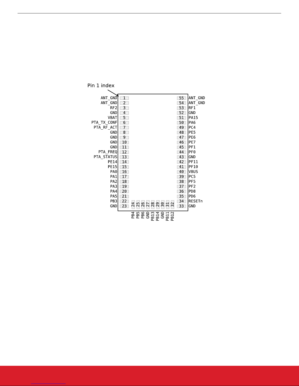
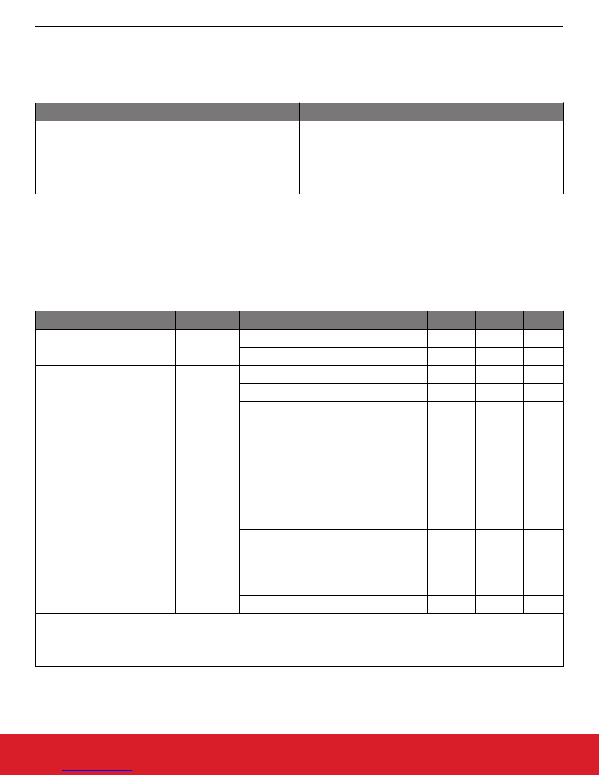
1. WGM160P Pinout
WGM160P is a 23.8 mm x 14.2 mm x 2.3 mm PCB module.
The diagram below describes pinout (top view)
UG384: WGM160P Hardware Design User’s Guide
WGM160P Pinout
silabs.com | Building a more connected world. Rev. 0.3 | 3
Figure 1.1. WGM160P Device Pinout
Page 4
UG384: WGM160P Hardware Design User’s Guide
2. WGM160P Pin Description
2.1 Pin Table
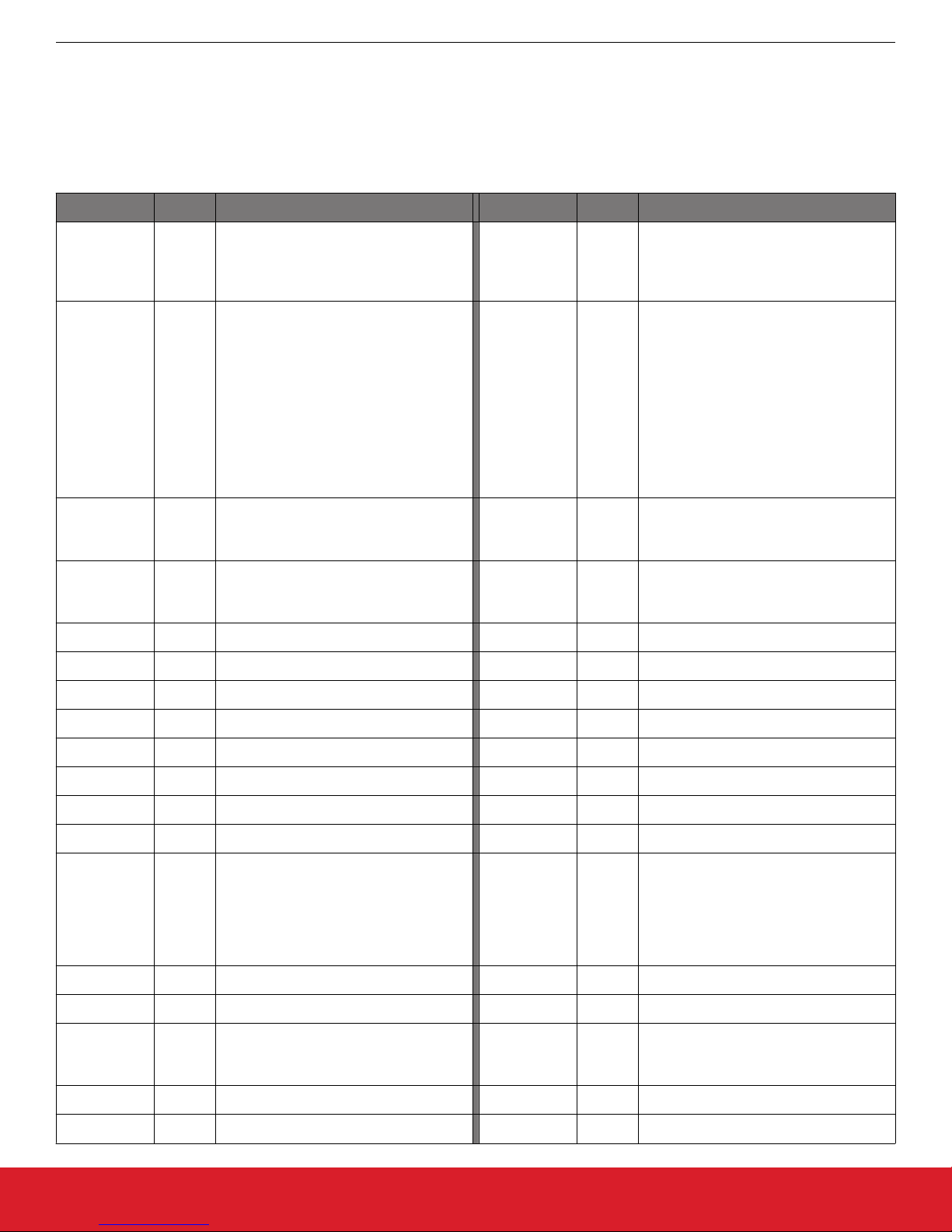
Table 2.1. WGM160P Device Pinout
Pin Name Pin(s) Description Pin Name Pin(s) Description
WGM160P Pin Description
1
ANT_GND
GND
PTA_TX_CO
NF
PTA_FREQ 12
PE14 14 GPIO
PA0 16 GPIO PA1 17 GPIO
2
Antenna ground.
54
55
4
8
9
10
11
Ground. Connect all ground pins to
23
ground plane.
27
30
33
43
52
PTA TX_CONF pin. These pins can be
6
used to manage co-existence with another 2.4 GHz radio.
PTA FREQ pin. These pins can be
used to manage co-existence with another 2.4 GHz radio.
RF2 3
VBAT 5 Module power supply
PTA_RF_AC
T
PTA_STA-
TUS
PE15 15 GPIO
7
13
External antenna connection for diversity antenna. Terminate to ground with
47-51 Ohms if not connected to an antenna.
PTA RF_ACT pin. These pins can be
used to manage co-existence with another 2.4 GHz radio.
PTA STATUS pin. These pins can be
used to manage co-existence with another 2.4 GHz radio.
PA2 18 GPIO PA3 19 GPIO
PA4 20 GPIO
PB3 22 GPIO PB4 24 GPIO
PB5 25 GPIO PB6 26 GPIO
PB13 28 GPIO PB14 29 GPIO
PB11 31 GPIO
Reset input, active low. This pin is internally pulled up to VBAT. To apply an
RESETn 34
PD8 36 GPIO PF2 37 GPIO
PF5 38 GPIO
VBUS 40
PF11 42 GPIO (5V) PF0 44 GPIO (5V)
PF1 45 GPIO (5V) PE7 46 GPIO
external reset source to this pin, it is required to only drive this pin low during
reset, and let the internal pull-up ensure
that reset is released.
USB VBUS signal and auxiliary input to
5 V regulator. May be left disconnected
if USB is unused.
PA5 21 GPIO
PB12 32 GPIO
PD6 35 GPIO
PC5 39 GPIO
PF10 41 GPIO (5V)
silabs.com | Building a more connected world. Rev. 0.3 | 4
Page 5
UG384: WGM160P Hardware Design User’s Guide
Pin Name Pin(s) Description Pin Name Pin(s) Description
WGM160P Pin Description
PE6 47 GPIO
PE5 48 GPIO
PC4 49 GPIO PA6 50 GPIO
External antenna connection on
PA15 51 GPIO RF1 53
WGM160P22N. Not connected on
WGM160P22A.
Note:
1.
GPIO with 5V tolerance are indicated by (5V).
2.2 Power Pin
The
WGM160P module is supplied through the VBAT pin. There is no need for external bypass capacitors as the ICs decoupling is
performed within the module. Note that, although the VBAT supply is variable, the maximum TX output power can be achieved only
when the supply is set to 3.3 V or higher.
Note that pin VBUS cannot be used to supply the module.
2.3 RESETn Pin
The WGM160P module is reset by driving the RESETn pin low. A weak internal pull-up resistor holds the RESETn pin high allowing it
to be left unconnected if no external reset source is required.
Note that when WGM160P is not powered, RESETn must not be connected to an active supply through an external pull-up resistor as
this could damage the device.
Note also that the WGM160P features Power On Reset to keep WGM160P in reset mode until VBAT is high enough. For more details,
refer to the MCU EFM32GG11 reference manual.
2.4 RF Pins
The WGM160P module is available with two RF configurations.
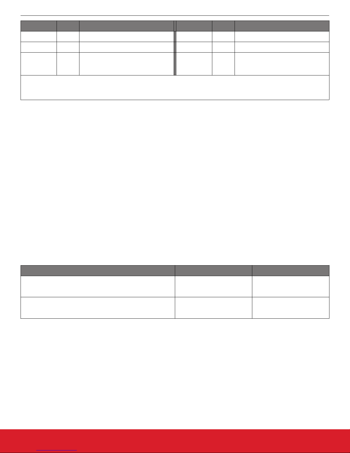
Table 2.2. WGM160P RF Configuration
Part Numbers RF1 RF2
WGM160PX22KGA2
Internal antenna.
RF port
WGM160P022KGA2
Pin RF1 is not connected.
WGM160PX22KGN2
RF port RF port
WGM160P022KGN2
RF ports are internally matched to 50 Ω.
It is recommended to connect any unused RF port to ground through a 50 Ω resistor. Any of
the RF ports can be used in a similar way. However, performance obtained on RF1 is slightly better, so it is preferable to use this one.
Only one RF port is active at a given time, but the module can also achieve antenna diversity if the application requires it. Port selection
and antenna diversity enablement are achieved through software configuration.
silabs.com | Building a more connected world. Rev. 0.3 | 5
Page 6
2.5 Clocks
The WGM160P module is available with two clock configurations.
Table 2.3. WGM160P Low Power Clock Configuration
Part Numbers Low Frequency Crystal
UG384: WGM160P Hardware Design User’s Guide
WGM160P Pin Description
WGM160PX22KGA2
Internal 32.768 kHz crystal
WGM160PX22KGN2
WGM160P022KGA2
No crystal
WGM160P022KGN2
A 32.768 kHz clock source is required to enable the lowest power operation in WiFi power save modes. 32.768 kHz can be generated
either an internal Low Frequency RC oscillator or an internal crystal. As the frequency tolerance of this clock affects wake-up
using
scheduling, power consumption in DTIM modes is optimized when using the WGM160P with an integrated 32.768 kHz crystal.
For WGM160P applications requiring Ethernet, a 50 MHz reference clock is required. This can be achieved either by connecting a 50
MHz external clock to module pin PB14 or by connecting a 50 MHz crystal oscillator between pins PB13 (HFXTAL_P) and PB14
(HFXTAL_N). For more details, refer to the MCU EFM32GG11 reference manual.
Table 2.4. WGM160P 50 MHz High-Frequency Crystal Oscillator
Parameter Symbol Test Condition Min Typ Max Unit
No clock doubling 4 — 50 MHz
Crystal frequency
f
HFXO
Clock doubler enabled 4 — 25 MHz
50 MHz crystal — — 50 Ω
Supported crystal equivalent ser-
ies resistance (ESR)
ESR
HFXO
24 MHz crystal — — 150 Ω
4 MHz crystal — — 180 Ω
Nominal on-chip tuning cap
1
range
On-chip tuning capacitance step
Startup time
Current consumption after startup
C
HFXO_T
SS
HFXO
t
HFXO
I
HFXO
Note:
1.
The effective load capacitance seen by the crystal will be C
two caps will be seen in series by the crystal.
On each of HFXTAL_N and
HFXTAL_P pins
50 MHz crystal, ESR = 50 Ω,
CL = 8 pF
24 MHz crystal, ESR = 150 Ω,
CL = 6 pF
4 MHz crystal, ESR = 180 Ω,
CL = 18 pF
50 MHz crystal — 880 — µA
24 MHz crystal — 420 — µA
4 MHz crystal — 80 — µA
/2. This is because each XTAL pin has a tuning cap and the
HFXO_T
8.7 — 51.7 pF
— 0.084 — pF
— 350 — µs
— 700 — µs
— 3 — ms
silabs.com | Building a more connected world. Rev. 0.3 | 6
Page 7
UG384: WGM160P Hardware Design User’s Guide
WGM160P Pin Description
2.6 PTA Pins
an RF transceiver using the same 2.4 GHz band (e.g. Bluetooth) is located next to WGM160P, a Packet Transfer Arbitration (PTA)
If
interface can be used to avoid mutual interference. In this case, the PTA pins are connected to the other transceiver. The PTA interface
is highly programmable and can use 1, 2, 3, or 4 pins upon configuration. PTA signal names can vary by manufacturer, so the table
below shows their alternative names.
Table 2.5. WGM160P PTA Configuration
WGM160P Pin # WGM160P Pin Name Alternative Name
6 PTA_TX_CONF GRANT
7 PTA_RF_ACT REQUEST
13 PTA_STATUS PRIORITY
12 PTA_FREQ RHO
PTA interface configuration is achieved through software configuration. PTA operation will be detailed in an upcoming application note.
2.7 Multifunction Pins
The multifunction pins refer to the WGM160P pins directly connected to the embedded MCU, EFM32GG11.
2.7.1 Software Architecture Considerations
As
described in the data sheet, the WGM160P module has considerable flexibility regarding the configuration of MCU pins, but not all
software architectures support all functions.
2.7.1.1 Bootloader
All devices come preprogrammed with a UART bootloader. This bootloader resides in flash and can be erased if it is not needed. More
information about the bootloader protocol and usage can be found in AN0003: UART Bootloader. Application notes can be found on the
Silicon Labs website (www.silabs.com/32bit-appnotes) or within Simplicity Studio in the [Documentation] area.
WGM160P pin 44 (GG11 PF0) and pin 45 (GG11 PF1) provide the bootloader with TX and RX access, respectively.
2.7.1.2 Implementation with GG11 Open Software
Full flexibility can be achieved when using the source software based on the Full MAC driver provided by Silicon Labs. The configuration of multifunction pins is accomplished within Simplicity Studio similar to the software development for the EFM32GG11. For more
details regarding these pins, refer to tables 6.2 and 6.3 of the WGM160P data sheet.
silabs.com | Building a more connected world. Rev. 0.3 | 7
Page 8

UG384: WGM160P Hardware Design User’s Guide
WGM160P Pin Description
2.7.1.3 Implementation with Gecko OS
following table provides details on the various multifunction pin features supported through Gecko OS 4.0. Features such as SPI
The
slave and USB will be supported in future releases of the Gecko OS.
Table 2.6. WGM160P Multifunction Pin Configuration With GeckoOS
WGM160P
Pin
GG11
Port
Default
Function
1
GPIO
(GOS_
GPIO_x)
2
UART
(GOS_
UART_x)
3
SPI
(GOS_
SPI_x)
I2C
(GOS_
I2C_x)
ADC
(GOS_
ADC_x)
PWM
(GOS_
PWM_x)
14 PE14 GPIO 0 0 0 TXD1
15 PE15 GPIO 1 - 1 TXD0
16 PA0
17 PA1
18 PA2
SPI Master
MOSI
SPI Master
MISO
SPI Master
CLK
2 SPI0 MOSI 6 2 TXEN
3 SPI0 MISO - 3 RXD1
4 SPI0 CLK 10 4 RXD0
19 PA3 GPIO 5 - 5 REFCLK
20 PA4 GPIO 6 11 6 CRSDV
21 PA5 GPIO 7 - 7 RXER
Bulk sflash
22 PB3
MOSI or
4
8 UART1 TX SPI1 MOSI - 8
UART TX
(logging)
Ethernet
(RMII)
Bulk sflash
MISO or 4
24 PB4
9 UART1 RX SPI1 MISO 12 9
UART RX
(logging)
25 PB5
26 PB6
UART RTS
(Com-
mands)
UART CTS
(Com-
mands)
10
11
UART0
RTS
UART0
CTS
- 10
1 11
28 PB13 GPIO 12 - -
29 PB14 GPIO 13 2 -
31 PB11
32 PB12
I2C Master
SDA
I2C Master
SCL
14 I2C0 SDA - 12
15 I2C0 SCL 3 13
Factory Re-
35 PD6
set
5
16
UART1
CTS
4 14
GPIO
36 PD8 GPIO 17
UART1
RTS
- 15
37 PF2 GPIO 18 5 16
silabs.com | Building a more connected world. Rev. 0.3 | 8
Page 9

UG384: WGM160P Hardware Design User’s Guide
WGM160P Pin Description
WGM160P
Pin
GG11
Port
Default
Function
1
GPIO
(GOS_
GPIO_x)
2
UART
(GOS_
UART_x)
3
SPI
(GOS_
SPI_x)
I2C
(GOS_
I2C_x)
ADC
(GOS_
ADC_x)
PWM
(GOS_
PWM_x)
38 PF5 GPIO 19 - 17
39 PC5 GPIO 20 - 18
41 PF10 USB DM 21 7 -
42 PF11 USB DP 22 - -
UART TX
46 PE7
(Com-
23 UART0 TX - 19
mands)
UART RX
47 PE6
(Com-
24 UART0 RX 8 20
mands)
48 PE5 GPIO 25 - 21
49 PC4
Bulk sflash
SCLK
26 SPI1 CLK - 22
50 PA6 GPIO 27 9 23 MDC
51 PA15 GPIO 28 - 24 MDIO
Ethernet
(RMII)
Note:
1.
The prefix _x in GOS_GPIO_x is replaced with the numbers in the column: GOS_GPIO_1, GOS_GPIO_2, etc. SDK have all
those symbols defined in header files.
2. All UART IO’s are relevant to WGM160P, so when RX is used it means WGM160P receives, and TX means WGM160P transmits.
3. SPI can be configured as master or slave. At the moment, only SPI master is supported in Gecko OS. SPI slave is coming in a
future release. SPI interface does not define fixed SPI_CS pin. CS is configurable and any unused GPIO can be used for this
function.
4. PB3 and PB4 showing 2 default functions means that those pins can be assigned using Gecko OS command API (variables and
command) to one of those functions. For example, “set bus.data_bus uart1” or “set system.bflash.port spi1”. Once one of these
variables is assigned, the other one will give an error that pins are already in use. UART (logging) is used to print Gecko OS log
messages: https://docs.silabs.com/gecko-os/4/standard/latest/cmd/variables/bus#bus-log-bus
5. WGM160P PAD 35 is used as factory reset pin and resets all Gecko OS variables to defaults. Any of the spare GPIOs is expected to be configured as factory reset pin, default being GOS_GPIO_16. More about factory reset at https://docs.silabs.com/gecko-
os/4/standard/latest/getting-started#performing-a-factory-reset.
silabs.com | Building a more connected world. Rev. 0.3 | 9
Page 10

UG384: WGM160P Hardware Design User’s Guide
Application Schematic Recommendations
3. Application Schematic Recommendations
3.1 Power Supply
The WGM160P consists of two main blocks, the microcontroller (EFM32GG11) and the Wi-Fi network co-processor (WF200). The microcontroller contains an internal dc-dc converter that powers both the microcontroller core and the WiFi chip with a lower supply voltage to reduce overall power consumption. All the internal supplies are connected together and supplied by module pin VBAT.
Care should be taken that the supply source is capable of supplying enough current for the load peaks of the power amplifier (which
can go momentarily up to 200 mA), so it is recommended to select a regulator capable of supplying 300 mA. The peaks can be very
fast, and the power supply for the module should be capable of reacting to load changes within 5 µs.
External high-frequency bypass capacitors are not needed because the module contains the required supply filter capacitors. However,
care should be taken to prevent strong switching noise from being superimposed on the supply lines. Such noise can be generated, for
example, by the onboard charge pump converters used in RS232 level shifters.
Note that there is a total of about 15 µF of low ESR ceramic capacitors inside the module connected directly on the supply input. When
using external regulators to generate regulated supplies for the module, the stability of the regulator with the low ESR provided by these
capacitors should be checked. Some low-drop linear regulators and some older switched mode regulators are not stable when ceramic
output capacitors are used. The data sheet of the regulator typically lists recommendations concerning suitable capacitors, including
data on ESR range and/or stability curves. A regulator should include the statement “stable with ceramic capacitors”.
3.2 RF Part
When using the WGM160P with an antenna external to the module, be they connectorized off-the-shelf antennas or PCB trace antennas, antenna impedance must be well matched to 50 Ω, achieving better than -10 dB return loss throughout the 2.4-2.48 GHz band to
reduce distortion in the module power amplifier due to impedance mismatch.
The matching should be verified in the final enclosure, and it is recommended to reserve SMD placeholders for external antenna tuning.
The suggested external antenna matching structure is a 3-element PI network.
Unused RF ports (RF2 on both variants or RF1 on the variant without the chip antenna assembled) must be terminated to ground with a
resistor of between 47 and 51 Ω.
silabs.com | Building a more connected world. Rev. 0.3 | 10
Page 11

UG384: WGM160P Hardware Design User’s Guide
4. Typical Application Schematics
The diagrams below show a simple application schematic with WGM160P and its internal antenna.
Typical Application Schematics
Figure 4.1. WFM160PX22KGA2 Schematics
silabs.com | Building a more connected world. Rev. 0.3 | 11
Page 12

UG384: WGM160P Hardware Design User’s Guide
Layout Recommendations
5. Layout Recommendations
5.1 Generic RF Layout Considerations
For custom designs, use the same number of PCB layers as are present in the reference design whenever possible. Deviation from the
reference PCB layer count can cause different PCB parasitic capacitances, which can detune the matching network from its optimal
form. If a design with a different number of layers than the reference design is necessary, make sure that the distance between the top
layer and the first inner layer is similar to that found in the reference design because this distance determines the parasitic capacitance
value to ground. Otherwise, detuning of the matching network is possible, and fine tuning of the component values may be required.
The Silicon Labs development kit uses a 1.6 mm thick FR4 PCB with the following board stack-up.
Figure 5.1. Reference Design PCB Specification
silabs.com | Building a more connected world. Rev. 0.3 | 12
Page 13

UG384: WGM160P Hardware Design User’s Guide
Layout Recommendations
Use as much continuous and unified ground plane metallization as possible, especially on the top and bottom layers.
as many ground stitching vias, especially near the GND pins, as possible to minimize series parasitic inductance between the
Use
ground pours of different layers and between the GND pins.
Use a series of GND stitching vias along the PCB edges and internal GND metal pouring edges. The maximum distance between the
vias should be less than lambda/10 of the 10th harmonic (the typical distance between vias on a reference design is 1 mm). This distance is required to reduce the PCB radiation at higher harmonics caused by the fringing field of these edges.
For designs with more than two layers, it is recommended to put as many traces (even the digital traces) as possible in an inner layer
and ensure large, continuous GND pours on the top and bottom layers, while keeping the GND pour metallization unbroken beneath
the RF areas (between the antenna, matching network and module). To benefit from parasitic decoupling capacitance, the inner layer
can be used to route the power supply with a wide VBAT sub-plane and traces to increase parasitic capacitance with nearby ground
layers.
Avoid using long and/or thin transmission lines to connect the RF-related components. Otherwise, due to their distributed parasitic inductance, some detuning effects can occur. Also, shorten the interconnection lines as much as possible to reduce the parallel parasitic
caps to the ground. However, couplings between neighbor discretes may increase in this way.
Route traces (especially the supply and digital lines) on inner layers for boards with more than two layers.
To achieve good RF ground on the layout, it is recommended to add large, continuous GND metallization on the top layer in the area of
the RF section (at a minimum). Better performance may be obtained if this is applied to the entire PCB. To provide a good RF ground,
the RF voltage potentials should be equal along the entire GND area as this helps maintain good VBAT filtering. Any gap on each PCB
layer should ideally be filled with GND metal and the resulting sections on the top and bottom layers should be connected with as many
vias as possible. The reason for not using vias on the entire GND section is due to layout restrictions, such as traces routed on other
layers or components on the bottom side.
Use tapered lines between transmission lines with different widths (i.e., different impedances) to reduce internal reflections.
Avoid using loops and long wires to obviate their resonances. They also work well as unwanted radiators, especially at the harmonics.
Avoid routing GPIO lines close or beneath the RF lines, antenna or crystal, or in parallel with a crystal signal. Use the lowest slew rate
possible on GPIO lines to decrease crosstalk to RF or crystal signals.
Use as many parallel grounding vias at the GND metal edges as possible, especially at the edge of the PCB and along the VBAT
traces, to reduce their harmonic radiation caused by the fringing field.
Place any high-frequency (MHz-ranged) crystal as close to the module as possible. External crystal load capacitors are not needed
since there is an on-chip capacitance bank for this purpose. Thus, it is suggested that one select crystals with load capacitance requirements that can be supported by the module. This way, the crystal can be placed close to the chip pins, and external capacitors are not
needed. Connect the crystal case to the ground using many vias to avoid radiation of the ungrounded parts. Do not leave any metal
unconnected and floating that may be an unwanted radiator. Avoid leading supply traces close or beneath the crystal or parallel with a
crystal signal or clock trace. If possible, use an isolating ground metal between the crystal and any nearby supply traces to avoid any
detuning effects on the crystal and to avoid the leakage of the crystal/clock signal and its harmonics to the supply lines. If possible,
route traces between crystal and module pins as differential signals to minimize the trace loop area.
5.2 RF-Pads Including the Diversity Port and External Antennas
With WGM160P variants without a chip antenna, the important properties are mainly to ensure that WGM160P ground pads are well
connected to the PCB ground plane in order to optimize thermal conductivity and prevent unwanted emissions due to ground currents.
The RF pads and RF traces conducting the RF signal should be dimensioned to have a characteristic impedance of 50 Ω. It is vital that
proper RF design principles be used when designing an application using the RF pads.
Antennas external to the module, be they connectorized off-the-shelf antennas or PCB trace antennas, must be well-matched to 50 Ω.
PCB size and layout recommendations from the antenna manufacturer must be followed. Board size, ground plane size, plastic enclosures, metal shielding, and components in close proximity to the antenna can affect the antenna impedance and radiation pattern.
Therefore, antenna matching should be verified in the final enclosure. Better than 10 dB return loss throughout the 2.4–2.48 GHz band
is recommended to prevent distortion in the module power amplifier due to impedance mismatch. PA distortion can cause significant
packet loss and poor overall performance.
silabs.com | Building a more connected world. Rev. 0.3 | 13
Page 14

UG384: WGM160P Hardware Design User’s Guide
Layout Recommendations
5.3 Module Chip Antenna
is common for very small antennas, the antenna on WGM160P uses the ground plane edge to radiate, rather than just the antenna
As
chip itself. The antenna on WGM160P is robust to the detuning effect of the proximity of various objects and makes the module easy to
use with a consistent and reliable performance. All the antenna needs is a small patch free from copper under the antenna end of the
module and a solid ground plane covering the whole PCB on at least one layer, especially the edge of the application board where the
antenna is placed. To prevent the RF signal coupling to other, sensitive parts of the design, it is recommended to have a solid, boardwide ground plane.
For optimal performance of the WGM160P Module, please follow these guidelines:
1. Place the Module at the edge of the PCB with the antenna end flush against the application board edge. If it is necessary to place
the module some distance from the edge, limit the copper plane edges to the level of the module antenna end.
2. Place the module close to the center of the edge of the board.
3. Do not place any metal (traces, components, battery, etc.) within the clearance area of the antenna.
4. Connect all ground pads directly to a solid ground plane covering the whole PCB. The grounds closest to the antenna end conduct
strong RF currents and are critical for good performance, while the rest of the ground pads are important for thermal conductivity.
5. Place multiple ground vias as close to the ground pads as possible. If possible, fill every unused area in all layers with groundconnected copper to improve thermal conductivity.
6. Terminate unused RF ports to ground with a resistor between 47 and 51 ohms
Figure 5.2. Top Layer Layout of WGM160P Reference Design
silabs.com | Building a more connected world. Rev. 0.3 | 14
Page 15

UG384: WGM160P Hardware Design User’s Guide
Layout Recommendations
Figure 5.3. Details of Antenna Ground Clearance
Figure 5.4. Details about Board Dimensions and Module Placement
Any metallic objects in close proximity to the antenna will distort the antenna's electromagnetic fields and cause the antenna center
frequency
to shift, reducing performance. The minimum recommended distance of metallic and/or conductive objects is 10 mm in any
direction from the antenna, except in the directions of the application PCB ground planes. Please note that even if nearby metallic objects do not shift the antenna's center frequency, they will still distort the radiation pattern and prevent the antenna from radiating freely.
Metals are opaque to radio frequencies and may create the equivalent of a shadow, a region of weaker performance, in the direction
covered by the metal.
silabs.com | Building a more connected world. Rev. 0.3 | 15
Page 16

UG384: WGM160P Hardware Design User’s Guide
Layout Recommendations
Figure 5.5. Enclosure Clearance Recommendations
Because the application board is part of the antenna circuit, its dimensions affect the antenna's efficiency and thus its achievable range.
Narrower ground planes can be used but will result in compromised RF performance.
The following two-dimensional radiation pattern plots have been measured on the BRD4321A board:
Figure 5.6. WGM160P Radio Board BRD4321A with XYZ Axis Added
silabs.com | Building a more connected world. Rev. 0.3 | 16
Page 17

UG384: WGM160P Hardware Design User’s Guide
Layout Recommendations
Figure 5.7. Typical 2D Radiation Pattern—Top View
silabs.com | Building a more connected world. Rev. 0.3 | 17
Page 18

UG384: WGM160P Hardware Design User’s Guide
Layout Recommendations
Figure 5.8. Typical 2D Radiation Pattern—Front View
silabs.com | Building a more connected world. Rev. 0.3 | 18
Page 19

UG384: WGM160P Hardware Design User’s Guide
Layout Recommendations
Figure 5.9. Typical 2D Radiation Pattern—Side View
silabs.com | Building a more connected world. Rev. 0.3 | 19
Page 20

6. Recommendations for Certification
Customers should refer to the datasheet for detailed recommendations about certification.
UG384: WGM160P Hardware Design User’s Guide
Recommendations for Certification
silabs.com | Building a more connected world. Rev. 0.3 | 20
Page 21

7. Package Outline
UG384: WGM160P Hardware Design User’s Guide
Package Outline
Figure 7.1. WGM160PX22KGA2 Package Outline
silabs.com | Building a more connected world. Rev. 0.3 | 21
Page 22

8. Recommended PCB Land Pattern
UG384: WGM160P Hardware Design User’s Guide
Recommended PCB Land Pattern
Figure 8.1. WGM160PX22KGA2/ WGM160P022KGA2 Recommended Land Footprint
For WGM160P modules without antenna, there is no need for PCB antenna clearance.
silabs.com | Building a more connected world. Rev. 0.3 | 22
Page 23

UG384: WGM160P Hardware Design User’s Guide
Recommended PCB Land Pattern
Figure 8.2. WGM160PX22KGN2/ WGM160P022KGN2 Recommended Land Footprint
silabs.com | Building a more connected world. Rev. 0.3 | 23
Page 24

Smart.
Connected.
Energy-Friendly.
Products
www.silabs.com/products
Disclaimer
Silicon Labs intends to provide customers with the latest, accurate, and in-depth documentation of all peripherals and modules available for system and software implementers using or
intending to use the Silicon Labs products. Characterization data, available modules and peripherals, memory sizes and memory addresses refer to each specific device, and "Typical"
parameters provided can and do vary in different applications. Application examples described herein are for illustrative purposes only. Silicon Labs reserves the right to make changes without
further notice to the product information, specifications, and descriptions herein, and does not give warranties as to the accuracy or completeness of the included information. Without prior
notification, Silicon Labs may update product firmware during the manufacturing process for security or reliability reasons. Such changes will not alter the specifications or the performance
of the product. Silicon Labs shall have no liability for the consequences of use of the information supplied in this document. This document does not imply or expressly grant any license to
design or fabricate any integrated circuits. The products are not designed or authorized to be used within any FDA Class III devices, applications for which FDA premarket approval is required
or Life Support Systems without the specific written consent of Silicon Labs. A "Life Support System" is any product or system intended to support or sustain life and/or health, which, if it fails,
can be reasonably expected to result in significant personal injury or death. Silicon Labs products are not designed or authorized for military applications. Silicon Labs products shall under no
circumstances be used in weapons of mass destruction including (but not limited to) nuclear, biological or chemical weapons, or missiles capable of delivering such weapons. Silicon Labs
disclaims all express and implied warranties and shall not be responsible or liable for any injuries or damages related to use of a Silicon Labs product in such unauthorized applications.
Trademark Information
Silicon Laboratories Inc.® , Silicon Laboratories®, Silicon Labs®, SiLabs® and the Silicon Labs logo®, Bluegiga®, Bluegiga Logo®, Clockbuilder®, CMEMS®, DSPLL®, EFM®, EFM32®,
EFR, Ember®, Energy Micro, Energy Micro logo and combinations thereof, "the world’s most energy friendly microcontrollers", Ember®, EZLink®, EZRadio®, EZRadioPRO®, Gecko®, Gecko
OS, Gecko OS Studio, ISOmodem®, Precision32®, ProSLIC®, Simplicity Studio®, SiPHY®, T elegesis, the Telegesis Logo®, USBXpress® , Zentri, the Zentri logo and Zentri DMS, Z-Wave®,
and others are trademarks or registered trademarks of Silicon Labs. ARM, CORTEX, Cortex-M3 and THUMB are trademarks or registered trademarks of ARM Holdings. Keil is a registered
trademark of ARM Limited. Wi-Fi is a registered trademark of the Wi-Fi Alliance. All other products or brand names mentioned herein are trademarks of their respective holders.
Silicon Laboratories Inc.
400 West Cesar Chavez
Austin, TX 78701
USA
Quality
www.silabs.com/quality
Support and Community
community.silabs.com
http://www.silabs.com
 Loading...