

Page 1
EZRadioPRO Dev Kit UG
EZRADIOPRO® DEVELOPMENT KITS USER’S GUIDE
1. Kits Overview
This user's guide describes the development kit s of the new EZRadioPRO wireless development kit family . Each kit
contains two RF nodes based on the Wireless Motherboard to support evaluation and development of sub-GHz RF
links with the different EZRadioPRO devices. RF pico board content of the different kits is listed in Table 1, and
content common to all kits is listed in Table 2.
Table 1. RF Pico Boards of the EZRadioPRO Development Kits
Qty Description Part Number
Si4060/Si4362 Development Kit 868 MHz 4060-868-PDK
1 Si4060 RF Transmitter Pico Board 868 MHz, 10 dBm 4060-PCE10B868-EK
1 Si4362 RF Receiver Pico Board 868 MHz 4362-PRXB868-EK
Si4063/Si4362 Development Kit 915 MHz 4063-915-PDK
1 Si4063 RF Transmitter Pico board 915 MHz, 20 dBm 4063-PCE20B915-EK
1 Si4362 RF Receiver Pico board 915 MHz 4362-PRXB915-EK
Si4461 Development Kit 868 MHz 4461-868-PDK
Si4438 Development Kit 490 MHz 4438-490-PDK
2 Si4438 RF Transceiver Pico board 490 MHz, 20 dBm, direct tie 4438-PCE20D490
2 Si4461 RF Transceive r Pico board 868 MHz, 14 dBm, direct tie 4461-PCE14D868-EK
Si4463 Development Kit 915 MHz 4463-915-PDK
2 Si4463 RF Transceiver Pico Board 915 MHz, 20 dBm, switched 4463-PCE20C915-EK
Table 2. Content Common to Every Kit
Qty Description Part Number
2 Wireless Motherboard MSC-WMB93X
2 C8051F930 MCU Pico Board UPPI-930-RF
2 USB cable (USBA-USB mini)
2 Antenna with SMA connection MSC-AT50-XXX
1 Kit user guide
Rev. 0.1 12/12 Copyright © 2012 by Silicon Laboratories EZRadioPRO Dev Kit UG
Page 2

EZRadioPRO Dev Kit UG
2. Software Setup
There are two software tools provided by Silicon Labs to aid in EZRadioPRO software development, the Wireless
Development Suite (WDS) and the Silicon Labs Integrated Development Environment (IDE). The recommended
starting point for EZRadioPRO development is the WDS software tool. This tool is able to identify the connected
boards by reading their identification memories (EBID) and provides valuable help by greatly simplifying radio
configuration, evaluation, and application development.
2.1. Hardware and Software Requirements for WDS
The following hardware and software is required to run the WDS:
Windows XP or later
Microsoft .NET framework 3.5 or later
Silicon Labs CP210x VCP driver
MCR v7.14 or later (Matlab compiler runtime for the modem calculator)
WDS v3.1.9.0 or later
The lack of the .NET framework and VCP driver are recognized during the WDS installation. The install wizard will
install the missing components after prompting the user for consent.
2.2. Download WDS
WDS can be obtained from the Silicon Labs web site free of charge at
http://www.silabs.com/Support%20Documents/Software/WDS3-Setup.exe
2.3. Installation Steps
If WDS is already installed on your machine, skip this section.
Note: Before installing this software, local administration rights must be obtained from your network administrator.
1. Start WDS3-Setup.exe.
2. Click “Next” to start the installation process.
3. Accept the license agreement by clicking the check box, and then press the “Next” bu tton.
4. Select the installation folder.
It is recommended to use the default folder, C:\Program Files\Silabs\WDS3
5. When your settings are confirmed, click “Install” to continue.
6. Click “Finish” to close the WDS Installer.
2 Rev. 0.1
Page 3
EZRadioPRO Dev Kit UG
3. Hardware Setup
After checking the kit contents against Tables 1 and 2, the kit can be put into operation by performing the steps
listed below.
Figure 1. Wireless Motherboard Top Markings
1. Insert an RF Pico board into the connectors labeled as CON1 and CON2 on the Wireless Motherboard
(WMB).
2. Insert a UPPI-930-RF MCU Pico Board into the connectors, J5, J6, J7, and J8, on the WMB. The dotted
corner of the F930 MCU has to point to the triangle symbol on the WMB.
3. Connect the antenna to the SMA connector on the RF Pico Board.
4. Set the SUPPLY SELECT switch to the USB position.
5. Set the MCU DC/DC switch to the OFF position.
6. Ensure that all the CURRENT MEASUREMENT jumpers are in place.
7. Start the WDS on your PC.
8. Using one of the USB cables in the kit, connect the WMB to the PC.
9. If necessary wait for Windows to install the debug interface driver.
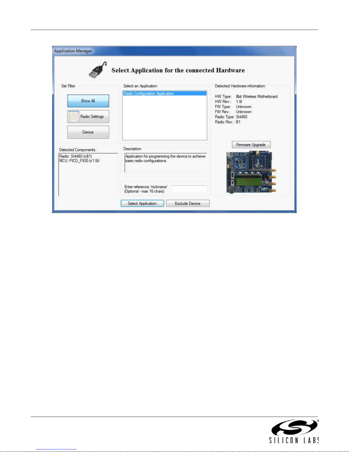
10. WDS must identify the connected board and open an Application Manager window that lists information
about the identified board.
11. Boards can be shipped without preloaded software, or the software on the board can be out of date; so,
upon first use or whenever the WDS is updated, it is advised to upgrade the firmware in the MCU of the
MCU Pico Board. Press the “Firmware Upgrade” button of the Application manager window.
12. Press “Continue” in the next window.
13. Select “Range test” in the next window and press the “Download” button. WDS downloads the new
firmware.
Rev. 0.1 3
Page 4
EZRadioPRO Dev Kit UG
Figure 2. WDS Application Manager Window
Repeat steps 1 to 11 for the other node of the kit.
The two nodes are now ready for the range test. For more details about the board’s operation, see "5. Wireless
Motherboard Hardware Platform" on page 6 and "6. Wireless Motherboard Schematics" on page 11.
A detailed description of the Range Test Application can be found in the application notes listed in “4. Useful
Documentation”.
The following is a quick-step guide to performing the Range Test:
1. Leave both nodes powered from USB as described above.
2. Button functions are always displayed on the bottom line of the LCD, directly above the buttons.
3. On the start screen that displays the chip type, press GO.
4. On the next screen, accept the default Function setting by pressing “” (right arrow).
5. Accept the default Frequency and Modulation setting by pressing “”.
6. Accept the default Data Rate and Deviation setting by pressing “”.
7. Accept the default Output Power setting by pressing “”.
8. Accept the default Packet settings by pressing “”.
9. Set the Destination ID to the Self ID of the other node by pressing “+”.
10. Accept ID setting by pressing “”.
11. Accept the default RSSI setting by pressing “”.
12. Press TX ON on the transmitter node; the other node will be the receiver.
In transceiver kits, the user defines which node will be the transmitter in the test by pressing TX ON on one of the
nodes. The boards start the test. The transmitter and transceiver nodes will display the number of packets sent; the
transceiver and receiver nodes will display the number of packets received and the PER value. If the PER value is
zero, the link is working correctly.
4 Rev. 0.1
Page 5

EZRadioPRO Dev Kit UG
4. Useful Documentation
For general information on the EZRadioPRO chips, see the following d ata sheets:
Si406x Data Sheet
Si4362 Data Sheet
Si446x Data Sheet
For hardware design guidance, see the following application notes:
AN627: Si4460/61 Low-Power PA Matching
AN629: Layout Design Guide for the Si4460/61/63/64 RF ICs
AN643: Si446x RX LNA Matching
AN648: Si4463/64 TX Matching
For detailed information on lab measurements and data sheet parameter verification, refer to the following
application notes:
AN655: Range Test Application for the EZRadioPRO Devices
AN632: WDS User Guide for Si446x and Si102x/3x Devices
For detailed information on programming the radio, re fer to the following documents:
Si406x API Descriptions
Si4362 API Descriptions
Si446x API Descriptions
AN633: Programming Guide for EZRadioPRO devices
Download WDS3 installer
Download Silicon Laboratories IDE installer
More useful documents can be accessed via the EZRadioPRO web pages at
http://www.silabs.com/products/wireless/EZRadioPRO/Pages/default.aspx
Rev. 0.1 5
Page 6
EZRadioPRO Dev Kit UG
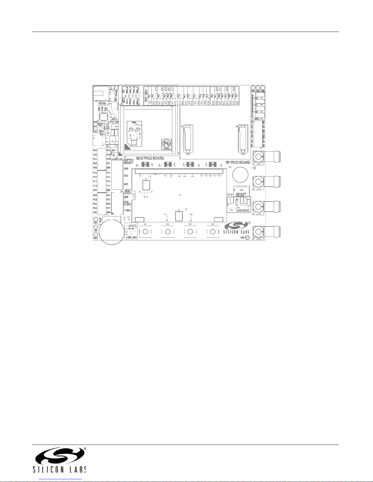
5. The Wireless Motherboard Hardware Platform
The wireless motherboard platform is a demo, evaluation, and development platform for EZRadioPRO radio ICs. It
consists of a wireless motherboard and interchangeable MCU and RF pico boards.
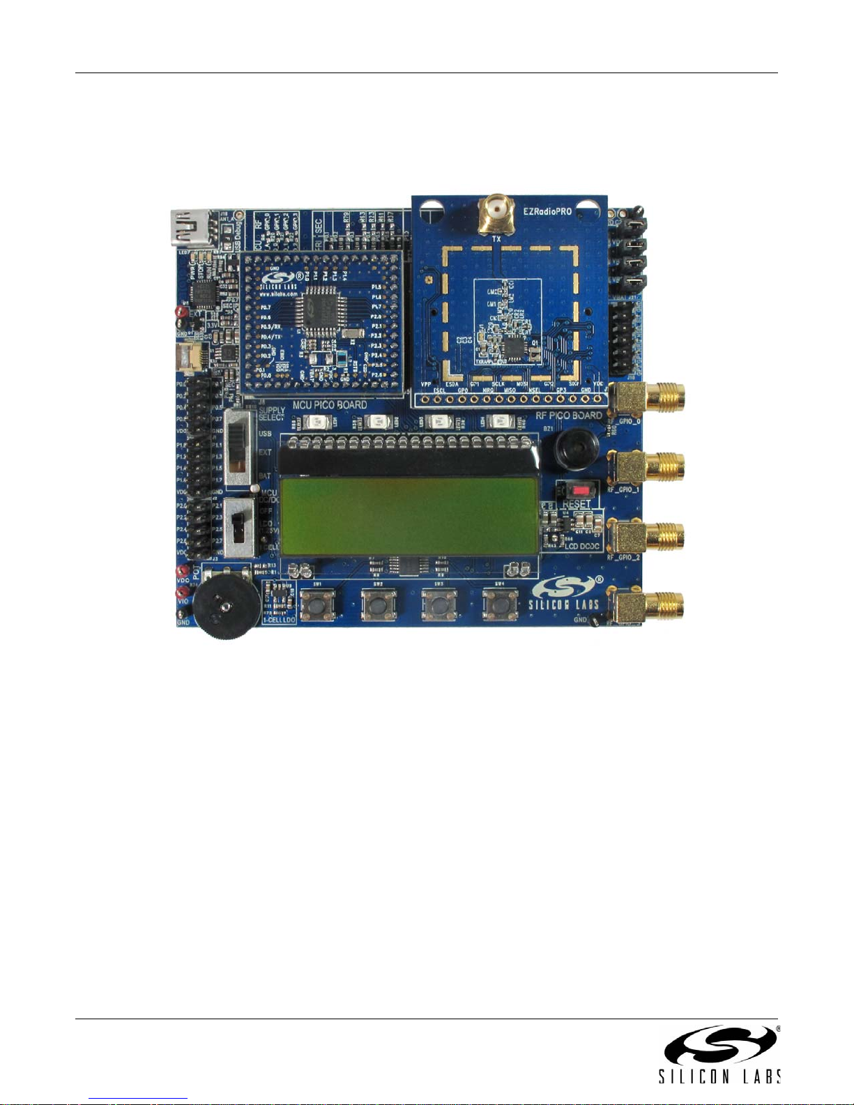
Figure 3. 8-bit Wireless Motherboard Platform
6 Rev. 0.1
Page 7

5.1. The Wireless Motherboard
MCU Pico Board RF Pico Board
Current
Measurement
Pins
Radio
Test
Pins
Radio GPIO
Connectors
BuzzerReset ButtonPush ButtonsPotentiometer
MCU DC/DC
Converter
Switch
MCU Test
Pins
Power
Supply
Switch
Sensor
Module
Connector
External
Power
Supply
Connection
USB
Communication
and Debug
Interface
EZRadioPRO Dev Kit UG
The wireless motherboard contains four pushbuttons, four LEDs, and a buzzer as simple user interfaces. A
graphical LCD displays menu items for range testing purposes and a potentiometer demonstrates analog
capabilities of the MCU. A switch supports the power options of the MCU's built-in dc/dc converter. Using the
current measurement jumpers, current consumption can be measured separately either for the MCU, the radio, or
the peripherals. The motherboard contains test pins for all I/O pins of the MCU and for all digital pins of the radio. In
addition, there are SMA connectors for the GPIOs of the radio for test equipment connection. A USB
communication interface as well as a built-in Silicon Labs USB-to-C2 debug adapter are integrated onto the board
so that the wireless motherboard (WMB) can be directly connected via USB to the PC for downloading and
debugging code on the MCU.
An interface connection towards sensor modules can also be found. The MCU is also connected to the RF pico
board through a connector pair.
Figure 4. Wireless Motherboard
Rev. 0.1 7
Page 8

EZRadioPRO Dev Kit UG
5.2. Power Scheme
The power source of the platform can be selected with the power supply selector switch “SUPPLY SELECT” on the
WMB board. If this switch is in the ”USB” position, supply voltage is provided by the PC that is connected to the
”J16” mini USB connector. If this switch is in the ”BAT” position, the supply voltage is provided by two AA batteries
in the battery holder on the bottom side of the board. If the ”SUPPLY SELECT” switch is in the ”EXT” position,
supply voltage is provided by an external power source through the ”TP7” and “TP9” points.
Using the ”MCU dc/dc” switch, the internal dc/dc converter of the C88051F930 MCU on the MCU pico board can
be activated if the connected pico boa rd supports this function. If th e switch is in ”OFF” positio n, the MCU's dc/dc
converter is inactive and the supply voltage is only determined by the state of the “SUPPLY SELECT” switch.
Positioning the switch to either ”LDO (1.25 V)” or ”1 CELL” position will turn on the MCU's dc/dc converter by
connecting 1.25–1.5 V supply voltage to the VBAT pin and removing external power from the VDC pin. The MCU
will provide 1.9 V in default setting on its VDC pin to all the other connected loads. Since this current is limited, it
may be necessary to disconnect or disable some loading part of the board. For further details, see the MCU data
sheet and the board schematic. The board schematic can be found in the EZRadioPRO Development Kit User's
Guide. A complete CAD design pack of the board is also available at www.silabs.com.
5.3. RF Pico Board
The RF pico board is a radio module that contains an EZRadioPRO radio IC, matching network and an SMA
connector on the top side. These components apart from the antenna connector are covered by a metal shield for
noise reduction. The digital signals of the radio (SCLK, SDI, SDO, NSEL, SCL, SDA, VDD and GND) can be
accessed on test points at the edge of the board. The boards also have a factory loaded board identification
memory (EBID) on the bottom side that contains data that des cribes the board pro perties. Via the unified RF pico
connector pair on the bottom side of the board, any RF pico board can be connected to the WMB.
8 Rev. 0.1
Figure 5. RF Pico Board Front Side
Page 9

EZRadioPRO Dev Kit UG
Table 3. Connections between the WMB Board and the RF Pico Board
Si446x, Si4362, Si406x, Si4438 WMB C8051F930
Pin Number Pin Name Pin Function RF Pico board J1
connector
EP,18 GND Ground 2 1,2,19,20 GND
8 VDD Voltage Supply input 1 17,18 VDD
11 NIRQ Interrupt output
active low
1 SDN Shutdown input
active high
15 NSEL SPI select input 6 6 P1.4
12 SCLK SPI clock input 9 5 P1.0
14 SDI SPI data input 7 3 P1.2
13 SDO SPI data output 8 4 P1.1
9 GPIO_0 General Purpose I/O 12 11 P2.6 (2nd)
10 GPIO_1 General Purpose I/O 11 12 P1.3
19 GPIO_2 General Purpose I/O 5 13 P2.5
20 GPIO_3 General Purpose I/O 4 14 P2.4
10 7 P0.1
38P2.3
WMB Con2
connector
Pin Name
Rev. 0.1 9
Page 10

EZRadioPRO Dev Kit UG
A schematic of an RF Pico Board can be found in the EZRadioPRO Development Kit User's guide. A complete
CAD design pack of all boards is also available at www.silabs.com.
Table 4. RF Pico Board Selection
Part Number Board Description
4060-PCE10B868 868 MHz matching, Transmitter, 10 dBm
4063-PCE20B915 915 MHz matching, Transmitter, 20 dBm
4362-PRXB868 868 MHz matching, Receiver
4362-PRXB915 915 MHz matching, Receiver
4461-PCE14D868 868 MHz matching, Transceiver, 14 dBm, Direct tied antenna connection
4463-PCE20C915 915 MHz matching, Transceiver, 20 dBm, TX/RX switched antenna connection
4438-PCE20D490 490 MHz matching, Transceiver, 20 dBm, Direct tie antenna connection
5.4. Setting up and Connecting the WMB to the PC
Steps for connecting the platform to the PC:
13. Connect an RF Pico Board to the WMB board through the CON 1 and CON2 connectors.
14. Insert a UPPI-930-RF MCU pico board in the conn ectors J5, J6, J7, J8 on the WMB. The dotted corne r of
the C8051F930 MCU has to point to the triangle symbol on the WMB.
15. Connect an antenna to the SMA connector on the RF Pico Board.
16. Select the desired power source with the SUPPLY SELECT switch.
17. Ensure that all the CURRENT MEASUREMENT jumpers are in place.
18. Connect the WMB board to a USB port of the PC.
19. Wait for Windows to install the driver of the debug interface if necessary.
10 Rev. 0.1
Page 11

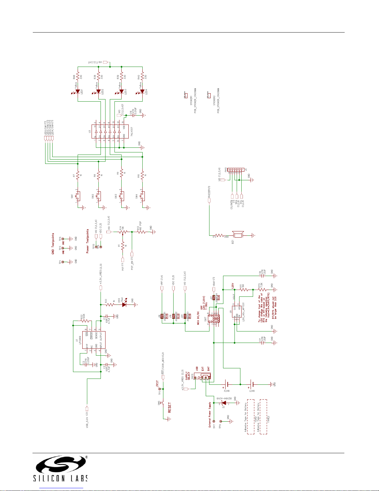
6. Wireless Motherboard Schematics
EZRadioPRO Dev Kit UG
Figure 6. Wireless Motherboard Schematic (1 of 4)
Rev. 0.1 11
Page 12

EZRadioPRO Dev Kit UG
12 Rev. 0.1
Figure 7. Wireless Motherboard Schematic (2 of 4)
Page 13
EZRadioPRO Dev Kit UG
Figure 8. Wireless Motherboard Schematic (3 of 4)
Rev. 0.1 13
Page 14

EZRadioPRO Dev Kit UG
14 Rev. 0.1
Figure 9. Wireless Motherboard Schematic (4 of 4)
Page 15

RF Section
RF EBID
50Ohm load
Si4463 Class-E +20 dBm matching for 915MHz
C1
2.2uF
C2
100nF
C3
100pF
C4
33pF
C5
100nF
Q1
30MHz
R7
4R7
1A02A13A24
VSS
5
SDA
6
SCL
7WP8
VCC
U3
24AA64T-I/MNY
C11 100nF
123456789
1011121314
15
J1
CM2
4.3pF
CM1
2.7pF
CR2
1.0pF
CR1
3.0pF
C0
3.3pF
LM1
10nH
LR1
18nH
CC2
56pF
LM3
8.2nH
LM2
10nH
LR2
22nH
L0
13nH
1
OUT1
2
GND
3
OUT2
4
VC25RF_IN6VC1
U2
uPG2214TB
CC1
56pF
SJ9
SJ10
LC3
120nH
C9
56pF
CM3
4.3pF
SJ1
1
TXRAMP
RF Shield
U4
SHIELD_BMI-S-203-F
TRX
CC3
56pF
1
SDN2RXP3RXN4TX5NC
6
VBATA
7
TXRAMP
8
VBATD
9
GPIO_0
10
GPIO_1
11
NIRQ
12
SCLK
13
SDO
14
SDI
15
NSEL
16
XOUT
17
XIN
18
GNDX
19
GPIO_2
20
GPIO_3
EP
EP
U1
SI4463
CM
4.7pF
12
34
56
78
910
11 12
13 14
15 16
17 18
19 20
RFP1
SFH31-NPPB-D10-SP_ASSYMETRIC
12
34
56
78
910
11 12
13 14
15 16
17 18
19 20
RFP2
SFH31-NPPB-D10-SP_ASSYMETRIC
PCB sticker
1
S1
PCB_STICKER_13X25MM
RF_SDN
RF_GPIO_3
RF_GPIO_2
RF_MOSI
RF_MISO
RF_SCLK
RF_NIRQ
RF_GPIO_0
RFVDD
RF_MOSI RF_MISO
RF_SCLK RF_NSEL
RF_NIRQ RF_SDN
RF_GPIO_0 RF_GPIO_1
RF_GPIO_2 RF_GPIO_3
RFVDD
RFVDD
EBID_SCL EBID_SDA
VPP
VPP
VPP
VPP
VPP
RF_SDN
RF_GPIO_3
RF_GPIO_2
RF_NSEL
RF_MOSI
RF_MISO
RF_SCLK
RF_NIRQ
RF_GPIO_1
RF_GPIO_0
EBID_SCL
EBID_SDA
RF_GPIO_1
RF_NSEL
RFVDD_TX
RF_GPIO_2
RF_GPIO_0
RXN
RXP
TX1
RFVDDRFVDD
RFVDD_TX
EZRadioPRO Dev Kit UG
Figure 10. RF Pico Board
Rev. 0.1 15
Page 16

EZRadioPRO Dev Kit UG
The information in this document is believed to be accurate in all respects at the time of publication but is subject to change without notice.
Silicon Laboratories assumes no responsibility for errors and omissions, and disclaims responsibility for any consequences resulting from
the use of information included herein. Additionally, Silicon Laboratories assumes no responsibility for the functioning of undescribed features or parameters. Silicon Laboratories reserves the right to make changes without further notice. Silicon Laboratories makes no warranty, representation or guarantee regarding the suitability of its products for any particular purpose, nor does Silicon Laboratories assume any
liability arising out of the application or use of any product or circuit, and specifically disclaims any and all liability, including without limitation
consequential or incidental damages. Silicon Laboratories products are not designed, intended, or authorized for use in applications intended to support or sustain life, or for any other application in which the failure of the Silicon Laboratories product could create a situation where
personal injury or death may occur. Should Buyer purchase or use Silicon Laboratories products for any such unintended or unauthorized
application, Buyer shall indemnify and hold Silicon Laboratories harmless against all claims and damages.
CONTACT INFORMATION
Silicon Laboratories Inc.
400 West Cesar Chavez
Austin, TX 78701
Tel: 1+(512) 416-8500
Fax: 1+(512) 416-9669
Toll Free: 1+(877) 444-3032
Please visit the Silicon Labs Technical Support web page:
https://www.silabs.com/support/pages/contacttechnicalsupport.aspx
and register to submit a technical support request.
Patent Notice
Silicon Labs invests in research and development to help our customers differentiate in the market with innovative low-power, small size, analogintensive mixed-signal solutions. Silicon Labs' extensive patent portfolio is a testament to our unique approach and world-class engineering team.
Silicon Laboratories and Silicon Labs are trademarks of Silicon Laboratories Inc.
Other products or brandnames mentioned herein are trademarks or registered trademarks of their respective holders.
16 Rev. 0.1
Page 17

Mouser Electronics
Authorized Distributor
Click to View Pricing, Inventory, Delivery & Lifecycle Information:
Silicon Laboratories:
4463-915-PDK
 Loading...