

Page 1
UG188: TS3300 EVB User's Guide
A 0.6–3.0 V IN, 1.8–3.6 V OUT, 3.5 µA, High-Efficiency Boost +
Output Load Switch
The demo board for the TS3300 is a completely assembled and tested circuit board that
can be used for evaluating the TS3300. The TS3300 is a power management product
that combines a high-efficiency boost regulator and an output load switch in one package.
The TS3300 includes an Anti-crush™ feature to prevent the collapse of the input voltage
to the boost regulator when the input is a weak (high impedance) source. If the input
voltage drops below a pre-determined voltage threshold (settable by a resistor divider),
the boost regulator switching cycles are paused, effectively limiting the minimum input
voltage. A pull-down resistor pad is available in order to set the anti-crush voltage.
The TS3300 boost regulator is set to an output voltage of 3.6 V via a resistor divider circuit. The TS3300 is fully specified over the –40°C to +85°C temperature range and is
available in a low-profile, thermally-enhanced 16-pin 3×3 mm TQFN package with an exposed back-side paddle. The product data sheet and additional documentation can be
found at www.silabs.com.
KEY FEATURES
• Boost Regulator
• Input Voltage: 0.6 V – 3 V
• Output Voltage: 3.6 V
• Shutdown Control Jumper
• Coilcraft 10 µH Inductor
(LPS4018-103ML)
•
Resistor Pad Available for Anti-Crush
Voltage Setting
™
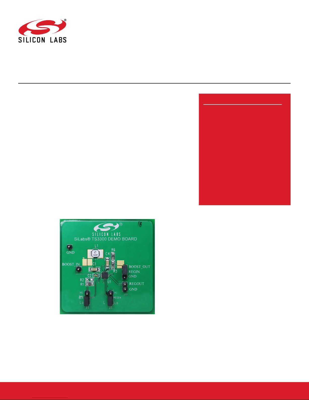
TS3300 Demo Board (Top View)
silabs.com | Smart. Connected. Energy-friendly. Rev. 1.1
Page 2
UG188: TS3300 EVB User's Guide
Functional Description
1. Functional Description
Boost Regulator Output Voltage Setting
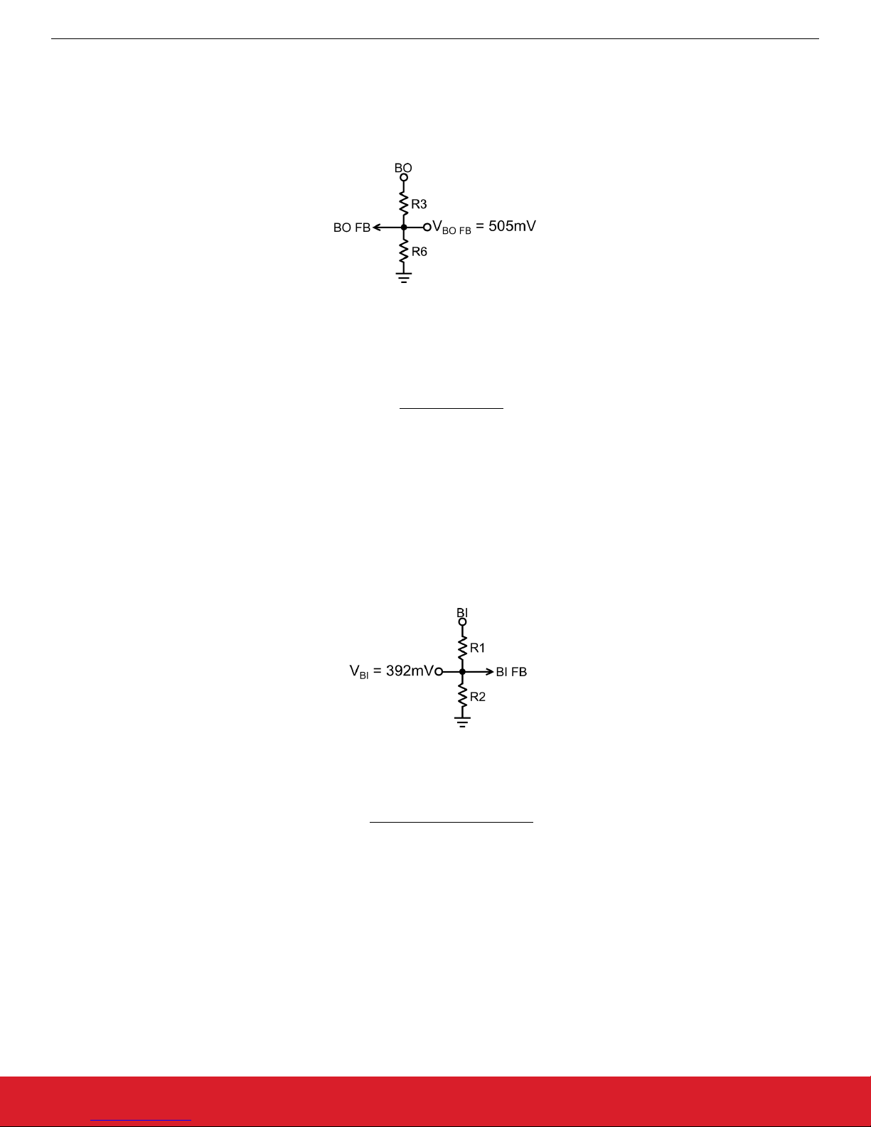
The TS3300 boost regulator is set to an output voltage of 3 V via a resistor divider circuit, as shown in the figure below.
Figure 1.1. Setting the Boost Output Voltage with a Voltage Divider
The output feedback (BO FB) pin is 505 mV. It is recommended to use large resistor values to minimize additional current draw at the
output. Resistors values less than 8 MΩ are recommended. Boost output voltage can be set by solving for R3 for a given R6 value in
the following equation:
VBO− 0.505)R6
(
R3 =
0.505
To set a 3 V output voltage with R6 = 1.37 MΩ, R3 is calculated to be 6.77 MΩ. A 1% standard resistor value of 6.81 MΩ is selected.
This results in an output voltage of 3.02 V.
Anti-Crush™ Voltage Setting
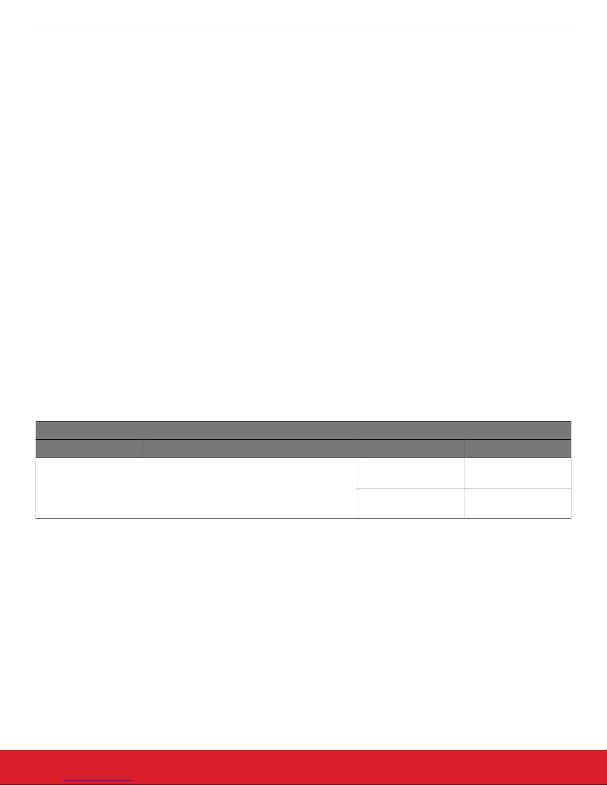
To set the anti-crush voltage, a feedback pin (BI FB) in conjunction with a voltage divider circuit can be implemented, as shown in the
figure below. The feedback pin voltage is 392 mV. It is recommended to use large resistor values to minimize additional current draw at
the input.
Figure 1.2. Setting the Anti-Crush Voltage with a Voltage Divider
Using the following equation to solve for R1 for a given R2 value, the output voltage can be set:
R1 =
V
(
ANTI −CRUSH
− 0.392)R2
0.392
To set a 0.8V output voltage with R2 = 1.37 MΩ, R1 is calculated to be 1.42 MΩ. A 1% standard resistor value of 1.37 MΩ is selected.
This results in an anti-crush voltage of 784 mV. The anti-crush voltage is to be set above the minimum input voltage specification of the
TS3300. Refer to the TS3300 Data Sheet “Applications Information” section for more details.
TS3300 Configurations
The TS3300 can be operated in either a Boost Only Configuration or in a Boost + Output Load Switch Configuration. The TS3300
Demo Board is designed so that both circuit configurations can be evaluated. Two sets of Quick-Start Procedures are provided, detailing how to evaluate each circuit configuration. If the Output Load Switch is not needed, it is recommended to use the Boost Only Configuration, since the lowest quiescent current is achievable this way.
silabs.com | Smart. Connected. Energy-friendly. Rev. 1.1 | 1
Page 3
UG188: TS3300 EVB User's Guide
Quick-Start Procedure
2. Quick-Start Procedure
2.1 Required Equipment
• TS3300 Demo Board
• 1.2 V Battery or Power Supply
• Two Digital Multimeters
• Oscilloscope
2.2 Boost + Output Load Switch Configuration
To evaluate the Boost + Output Load Switch configuration, the following steps should be performed:
1. Connect Jumper J1 LOW. The pin should be connected to the Lo pin, otherwise PCB ground.
2. Connect the provided Jumper so that the REGIN pin is connected to the BOOST_OUT pin.
3. Connect Jumper J3 LOW. The REGEN pin should be connected to the Lo pin, otherwise PCB ground.
4. Connect the battery positive terminal to the test point labeled BOOST_IN. Connect the negative terminal of the battery to the test
point labeled GND.
5. To monitor the boost regulator output voltage, connect the positive terminal of the voltmeter to the test point labeled BOOST_OUT.
Connect the negative terminal of the voltmeter to the test point labeled GND. Connect the Oscilloscope probe to the test point labeled BOOST_OUT to monitor the output ripple. The BOOST_OUT voltage should be regulated at approximately 3.02 V.
6. To monitor the output load switch voltage, V
REGOUT
OUT. Connect the negative terminal of the voltmeter to the test point labeled GND. The REGOUT voltage should be regulated at
approximately 3.02 V. Connect the Oscilloscope probe to the test point labeled REGOUT to monitor the output load switch.
7. To disable the Output Load Switch, connect Jumper J3 HIGH. The REGEN pin should be connected to the Hi pin, otherwise REGIN. The output load switch voltage, V
REGOUT
8. To enable the Output Load Switch, connect Jumper J3 LOW. The REGEN pin should be connected to the Lo pin, otherwise PCB
ground. The output load switch voltage, V
REGOUT
, connect the positive terminal of the voltmeter to the test point labeled REG-
, should drop to 0 V.
, should be approximately equal to V
BOOST_OUT
.
Table 2.1. Output Load Switch settings for Boost + Output Load Switch Configuration
Output Load Switch Function
REG FB SW EN REG IN REG EN Function
High
V
REGOUT
= GND
(OFF State)
REG FB, SW EN, REGIN should be connected to BO.
Low V
REGOUT
= V
BO
(ON State)
2.3 Boost Only Configuration
To evaluate the Boost Only configuration, the following steps should be performed:
1. Connect Jumper J1 LOW. The BENb pin should be connected to the Lo pin, otherwise PCB ground.
2. Connect the provided Jumper so that the REGIN pin is connected to the GND pin.
3. Connect Jumper J3 LOW. The REGEN pin should be connected to the LO pin, otherwise PCB ground.
4. Connect REGOUT to PCB Ground.
5. Connect the battery positive terminal to the test point labeled BOOST_IN. Connect the negative terminal of the battery to the test
point labeled GND.
6. To monitor the boost regulator output voltage, connect the positive terminal of the voltmeter to the test point labeled BOOST_OUT.
Connect the negative terminal of the voltmeter to the test point labeled GND. Connect the Oscilloscope probe to the test point labeled BOOST_OUT to monitor the output ripple. The BOOST_OUT voltage should be regulated at approximately 3.02 V.
7. To shutdown the boost regulator, connect Jumper J1 HIGH. The BENb pin should be connected to the Hi pin, otherwise
BOOST_IN. The boost output voltage, V
BOOST_OUT
, should drop to 0 V. The input supply current reduces to 0.1 µA.
silabs.com | Smart. Connected. Energy-friendly. Rev. 1.1 | 2
Page 4

3. Schematics
UG188: TS3300 EVB User's Guide
Schematics
Figure 3.1. TS3300 Demo Board Circuit Schematic
silabs.com | Smart. Connected. Energy-friendly. Rev. 1.1 | 3
Page 5

UG188: TS3300 EVB User's Guide
Figure 3.2. Top Silkscreen Figure 3.3. Top Layer #1
Schematics
Figure 3.4. Top Layer #2 Figure 3.5. Top Layer #3
Figure 3.6. Bottom Layer Figure 3.7. Bottom Silkscreen
silabs.com | Smart. Connected. Energy-friendly. Rev. 1.1 | 4
Page 6

4. Ordering / Component List
Ordering Number Description
TS3300DB TS3300 Demo Board
Designation Quantity Description
L1 1 10 µH ±20% Shielded Inductor (4×4 mm)
C1, C4 2 22 µF ±10% capacitor
UG188: TS3300 EVB User's Guide
Ordering / Component List
Table 4.1. TS3300 Ordering Information
Table 4.2. TS3300 Component List
LPS4018-103ML
(X5R) (25 V) (1206) GRM31CR61E226KE15L
C2 1 3.3 nF ±10% capacitor (0603), 445-5084-2-ND
R1, R6 2 1.37 MΩ ± 1% (0805), 311-1.37MCRTR-ND
R3 1 6.81 MΩ ± 1% (0805), 311-6.81MCRTR-ND
U1 1 TS3300
BOOST, BOOST_OUT, REG_OUT, GND (2) 5 Test points
J1, J3, REG_IN 3 Jumper
silabs.com | Smart. Connected. Energy-friendly. Rev. 1.1 | 5
Page 7

Smart.
Connected.
Energy-Friendly.
Products
www.silabs.com/products
Disclaimer
Silicon Laboratories intends to provide customers with the latest, accurate, and in-depth documentation of all peripherals and modules available for system and software implementers using
or intending to use the Silicon Laboratories products. Characterization data, available modules and peripherals, memory sizes and memory addresses refer to each specific device, and
"Typical" parameters provided can and do vary in different applications. Application examples described herein are for illustrative purposes only. Silicon Laboratories reserves the right to
make changes without further notice and limitation to product information, specifications, and descriptions herein, and does not give warranties as to the accuracy or completeness of the
included information. Silicon Laboratories shall have no liability for the consequences of use of the information supplied herein. This document does not imply or express copyright licenses
granted hereunder to design or fabricate any integrated circuits. The products are not designed or authorized to be used within any Life Support System without the specific written consent
of Silicon Laboratories. A "Life Support System" is any product or system intended to support or sustain life and/or health, which, if it fails, can be reasonably expected to result in significant
personal injury or death. Silicon Laboratories products are not designed or authorized for military applications. Silicon Laboratories products shall under no circumstances be used in
weapons of mass destruction including (but not limited to) nuclear, biological or chemical weapons, or missiles capable of delivering such weapons.
Trademark Information
Silicon Laboratories Inc.® , Silicon Laboratories®, Silicon Labs®, SiLabs® and the Silicon Labs logo®, Bluegiga®, Bluegiga Logo®, Clockbuilder®, CMEMS®, DSPLL®, EFM®, EFM32®,
EFR, Ember®, Energy Micro, Energy Micro logo and combinations thereof, "the world’s most energy friendly microcontrollers", Ember®, EZLink®, EZRadio®, EZRadioPRO®, Gecko®,
ISOmodem®, Precision32®, ProSLIC®, Simplicity Studio®, SiPHY®, Telegesis, the Telegesis Logo®, USBXpress® and others are trademarks or registered trademarks of Silicon Laboratories Inc. ARM, CORTEX, Cortex-M3 and THUMB are trademarks or registered trademarks of ARM Holdings. Keil is a registered trademark of ARM Limited. All other products or brand
names mentioned herein are trademarks of their respective holders.
Silicon Laboratories Inc.
400 West Cesar Chavez
Austin, TX 78701
USA
Quality
www.silabs.com/quality
Support and Community
community.silabs.com
http://www.silabs.com
 Loading...