

Page 1
Telegesis™
TG-ETRX357DVK-PM-012-112
ETRX357DVK Development Kit
Product Manual 1.12
©2016 Silicon Labs ETRX357DVK Product Manual (Rev 1.12)
ETRX357DVK – TELEGESIS DEVELOPMENT KIT FOR ZIGBEE®
TECHNOLOGY
PRODUCT MANUAL
Telegesi s™ is a tr ad em ar k o f Sil i con Laborator i es Inc.
Page 2
ETRX357 Development Kit
©2016 Silicon Labs - 2 - ETRX357DVK Product Manual (Rev 1.12)
1 ETRX357DVK – Development Kit Functional Summary
Devkit Features
ZigBee Networking “Out-of-the-Box”
Low cost evaluation platform for ZigBee wireless mesh
networking
Designed to set up a ZigBee mesh network in only a few
minutes without the need for any embedded software
The freely downloadable Telegesis Terminal Software
application offers an easy to use interface to the modules on
the development boards.
Also works with 3rd party terminal software like
HyperTerminal.
Broad selection of modules allows range testing of any
possible module/antenna combination.
Seamlessly Integrates into the Silicon Labs InSight Toolchain
Development boards can be used as hardware platform for
trials
Battery option allows easy prototyping of end devices
USB Drivers available for Windows from
www.silabs.com/telegesissoftware
Module Features
Based on the Silicon Labs EM357 single chip ZigBee/
IEEE802.15.4 solutions
2.4GHz ISM Band
Industry’s first ARM® Cortex-M3 based family of ZigBee
modules
192kB flash and 12kB of RAM
24 general-purpose I/O lines including analogue inputs (all
GPIOs of the EM357 are accessible)
Lowest Deep Sleep Current of sub 1µA and multiple sleep
modes
The Telegesis ETRX357-DVK
development kit is an ideal starting point
for development and evaluation of the
ETRX357 series low power 2.4GHz
ZigBee modules.
The ETRX357 modules are based on the
third generation Silicon Labs EM357
chipset offering the industry’s highest
wireless networking performance and
application code space at the lowest
power consumption.
The modules’ unique AT-style command
line interface allows designers to quickly
integrate ZigBee technology without
complex software engineering. For
custom application development the
ETRX357 development kits integrate with
ease into Silicon Labs’ InSight
development environment.
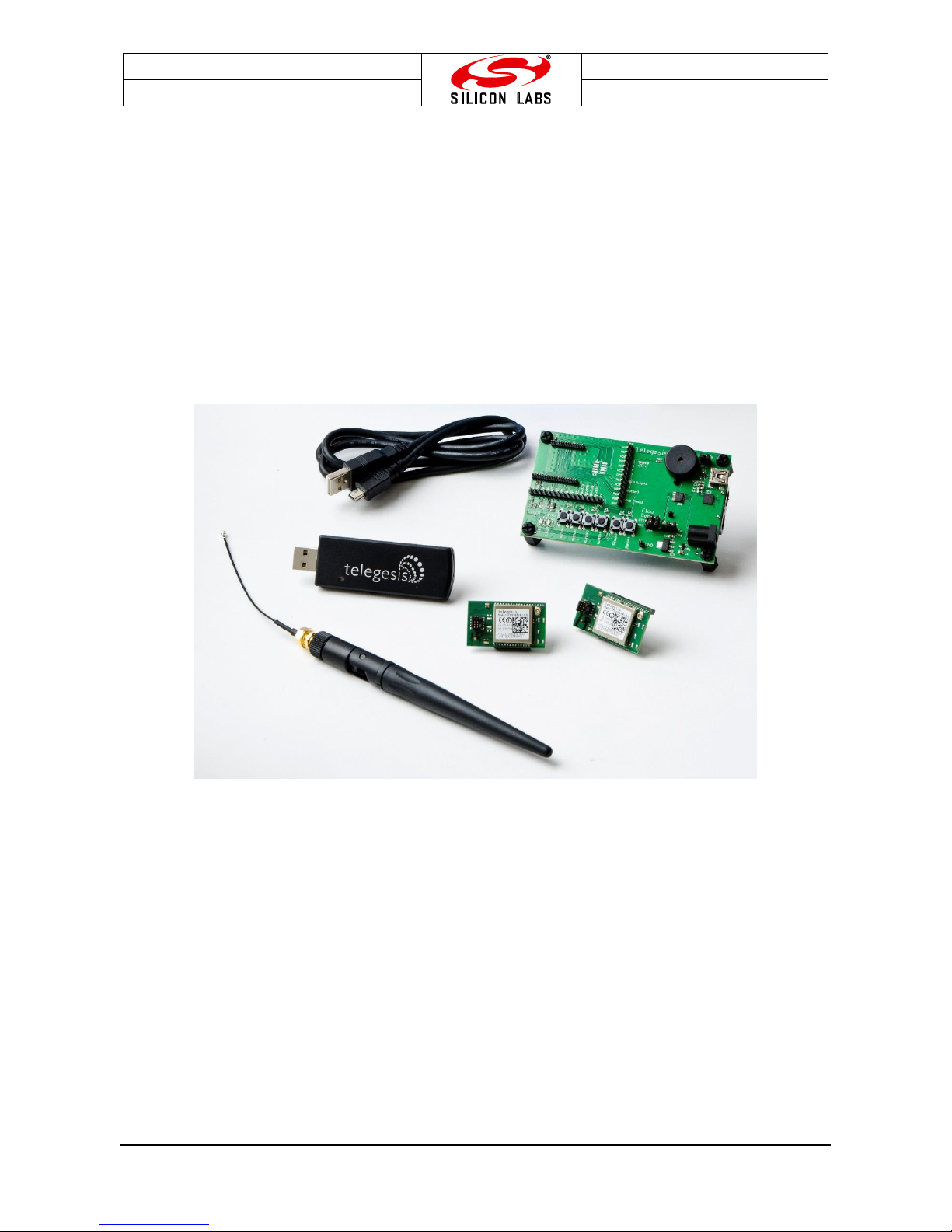
Development Kit Contents
3 x USB Development Boards
3 x USB Cable
2 x ETRX357 on Carrier-Board
2 x ETRX357HR on Carrier-Board
2 x ETRX357-LRS on Carrier-Board
2 x ETRX357HR-LRS on Carrier-Board
1 x ETRX3USB stick
2 x ½-wave Antenna
2 x ¼-wave Stubby Antenna
Development Board Features
Power can be supplied via USB, Power
Jack or on board battery holder (2xAAA)
Access to the Silicon Labs InSight Port
Light and Temperature sensor
4 x Buttons, 2 x LEDs, 1 x Buzzer
Reset and Bootload Button
USB to Serial converter
Breakout of all GPIO pins
Example AT-Style Commands
AT+BCAST Sends a Broadcast
AT+UCAST:<address> Sends a Unicast
AT+EN Establish PAN network
AT+JN Join PAN
Page 3

ETRX357 Development Kit
©2016 Silicon Labs - 3 - ETRX357DVK Product Manual (Rev 1.12)
Table of Contents
1 ETRX357DVK – DEVELOPMENT KIT FUNCTIONAL SUMMARY .................................... 2
2 ABSOLUTE MAXIMUM RATINGS OF THE DEVBOARD .................................................. 4
3 OPERATING CONDITIONS OF THE DEVBOARD ............................................................. 4
4 ELECTRICAL SPECIFICATIONS ....................................................................................... 4
4.1 Power supplies ................................................................................................................. 4
4.2 ZigBee modules ............................................................................................................... 4
5 INTEROPERABILITY ......................................................................................................... 5
6 OVERVIEW ......................................................................................................................... 5
6.1 The Development Board .................................................................................................. 6
6.2 The carrier board.............................................................................................................. 6
6.3 What’s in the ETRX357DVK box? .................................................................................... 7
7 SETTING UP THE HARDWARE ......................................................................................... 8
8 ETRX357 PINOUT .............................................................................................................. 8
9 THE DEVELOPMENT BOARD ......................................................................................... 10
9.1 Development Board Interface Description ...................................................................... 10
9.2 Development Board Sensors ......................................................................................... 12
10 THE CARRIER BOARD .................................................................................................... 13
11 DRIVER INSTALLATION AND OPERATION ................................ ................................... 13
11.1 Windows 9x/XP/2k Driver Installation ............................................................................. 13
12 APPLICATION SOFTWARE ............................................................................................. 17
12.1 Software Set-up ............................................................................................................. 18
12.2 Features of the Telegesis Terminal Application for ETRX357 ........................................ 18
The buttons .................................................................................................................... 18
The device window ......................................................................................................... 18
The menu bar ................................................................................................................. 19
12.3 A Quick Start .................................................................................................................. 20
Select the correct set of buttons ..................................................................................... 20
Network Setup ............................................................................................................... 20
Mesh networking ............................................................................................................ 21
Node types ..................................................................................................................... 21
12.4 Configuring Buttons for your Setup ................................................................................ 22
12.5 Using LEDs and ADCs on the ETRX357 ........................................................................ 23
12.6 Temperature display ...................................................................................................... 24
13 FIRMWARE UPGRADES ................................................................................................. 25
13.1 Firmware Upgrades via Serial Port ................................................................................. 25
13.2 Over the Air Firmware Upgrades .................................................................................... 27
ETRX2 and ETRX357 features ...................................................................................... 27
Passthrough with an ETRX357 ...................................................................................... 27
Recovering on the default channel ................................................................................. 28
14 HARDWARE ENHANCEMENT KIT .................................................................................. 29
15 DEVBOARD SCHEMATIC ................................................................................................ 30
16 CARRIER BOARD SCHEMATIC ...................................................................................... 32
17 ETRX357 ORDERING INFORMATION ............................................................................. 33
Page 4

ETRX357 Development Kit
©2016 Silicon Labs - 4 - ETRX357DVK Product Manual (Rev 1.12)
2 Absolute Maximum Ratings of the Devboard
Parameter
Min.
Max.
Units
Condition
Supply Voltage VDD
-0.3 9 V
Voltage on any I/O pin
-0.3
3.3
V
Storage Temperature range
-50
85
°C
Without batteries inserted
Table 1: Absolute Maximum Ratings
The absolute maximum ratings given above should under no circumstances be violated. Stress
exceeding one or more of the limiting values may cause permanent damage to the device.
Caution! ESD sensitive devices. Precautions should be used when handling the device
in order to prevent permanent damage.
3 Operating Conditions of the Devboard
Typical values at 5V 25°C.
Parameter
Min.
Typ.
Max.
Units
Condition
Supply Voltage, VDD
4 5 6 V
Supply Current
150
mA
TX with LRS-Module
Operating ambient temperature range
-20
25
40
°C
Range may be more
limited when batteries
are inserted. Consult
datasheets applicable
to your batteries
Table 2. Operating Conditions
The voltage regulators used are protected against overtemperature and overcurrent.
4 Electrical Specifications
4.1 Power supplies
Only use a mains adaptor that has been certified as a low power source according to IEC60950-1.
The power from the USB connection should be restricted in line with the requirements of IEC 60950-
1. PCs approved to IEC 60950-1 will meet this requirement.
Only good quality (vented) alkaline batteries should be used. Ensure they are inserted with the
correct polarity. Note that they may restrict the working temperature range of the equipment.
4.2 ZigBee modules
See ETRX357 and ETRX357-LRS Product Manuals
Page 5

ETRX357 Development Kit
©2016 Silicon Labs - 5 - ETRX357DVK Product Manual (Rev 1.12)
5 Interoperability
Unless otherwise specified the Development kits ships with Telegesis R3xx firmware based on
EmberZNet4.x. Please note that the R3xx Telegesis AT-Command line interpreter is based on
ZigBee PRO, but most of the functionality is implemented as a private application profile.
Interoperability with wireless mesh networking solutions from other manufacturers is only possible
when knowing the application profile specification of this device and using the provided transparent
commands. If this is a concern please contact us for advice. Telegesis also offer separate firmware
specifically developed for Home Automation and Smart Energy applications.
6 Overview
The ETRX357DVK development kit has been designed to allow quick evaluation and prototyping
using the ETRX357 ZigBee modules.
This document is intended to describe the hardware and accompanying software of the development
kits. To learn more about the usage of the ETRX357 module please refer to the following documents:
TG-ETRX357-PM-010-xxx: ETRX357 Product manual
TG-ETRX357-LRS-PM-015-xxx: ETRX357-LRS (long range) Product manual
TG-ETRX357USB-PM-014-xxx: ETRX3 USB stick Product manual
TG-ETRXn-R3xx-Commands: AT Style command dictionary for firmware R3xx
All our documents can be found at www.silabs.com/telegesisdocuments.
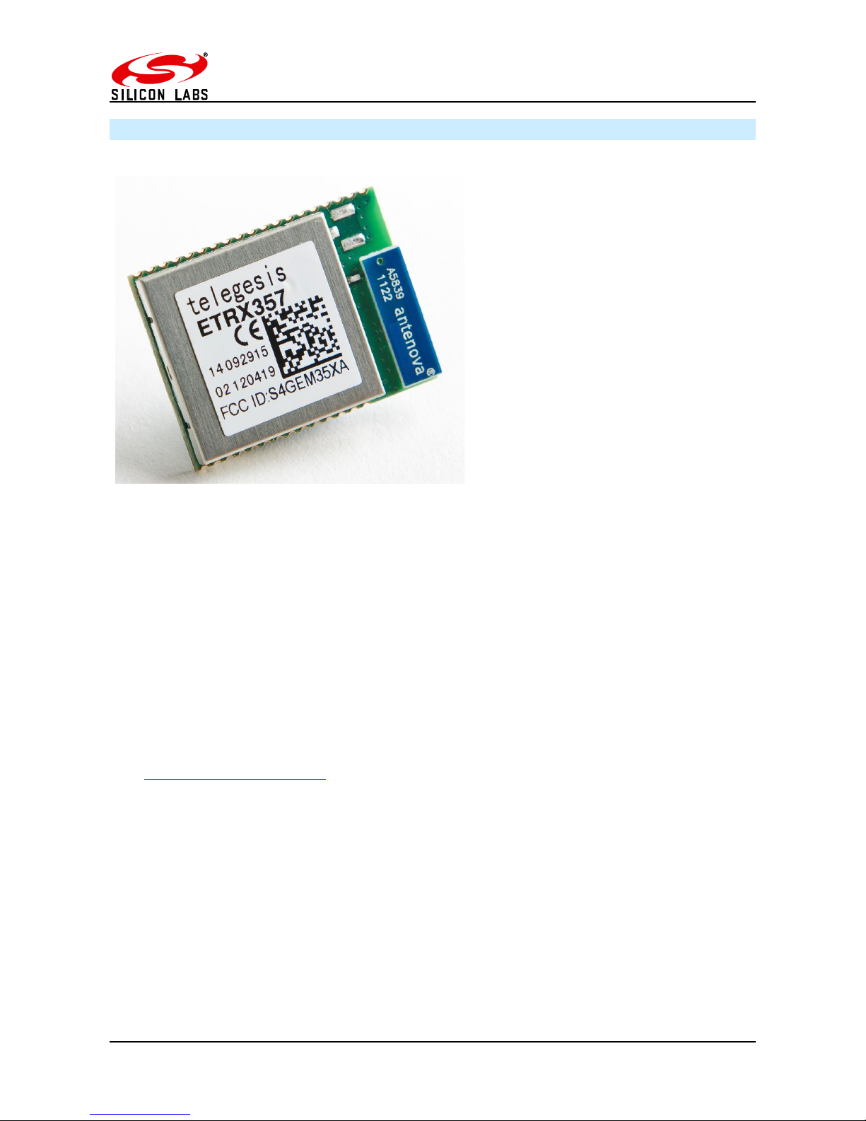
The ETRX357 module is available in four variants:
ETRX357 – with on-board ceramic antenna and 8dBm output power
ETRX357HR – with Hirose coaxial connector and 8dBm output power
ETRX357-LRS – with on-board ceramic antenna, LNA and 19dBm output power
ETRX357HR-LRS – with Hirose coaxial connector, LNA and 19dBm output power
Page 6
ETRX357 Development Kit
©2016 Silicon Labs - 6 - ETRX357DVK Product Manual (Rev 1.12)
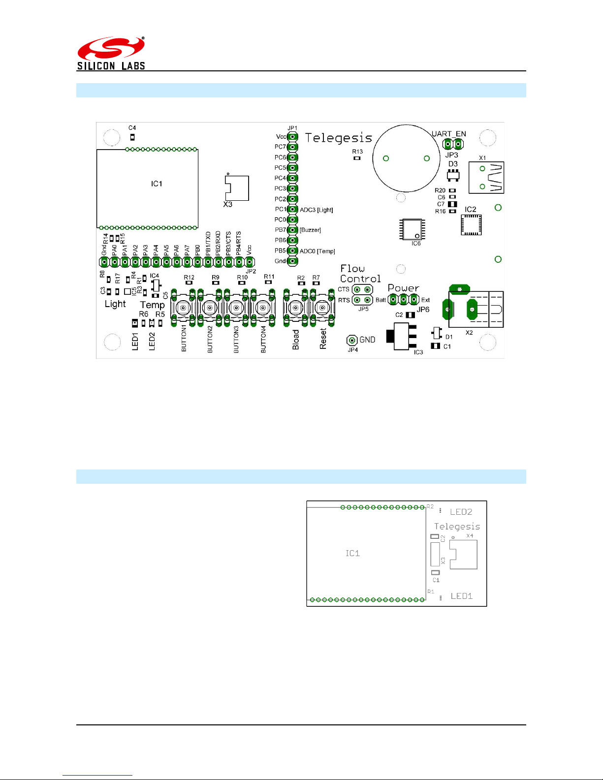
6.1 The Development Board
Figure 1. The development board
The development board which is part of the development kit hosts a USB to serial bridge as well as
voltage regulation circuitry. Furthermore it hosts a reset switch, a bootloader switch, 4 buttons, 2
LEDs and a beeper, all of are connected to the I/Os of the module as described later in this document.
6.2 The carrier board
The carrier board has an ETRX357 module
plus two LEDs, and a connector to attach to a
Silicon Labs InSight Adaptor for reflashing the
firmware. It plugs on to the development board.
Figure 2. The carrier board
Page 7

ETRX357 Development Kit
©2016 Silicon Labs - 7 - ETRX357DVK Product Manual (Rev 1.12)
6.3 What’s in the ETRX357DVK box?
- 3 x ETRX357DV Development Boards
- 3 x USB cables
- 2 x ETRX357 on carrier boards
- 2 x ETRX357HR on carrier boards
- 2 x ETRX357-LRS on carrier boards
- 2 x ETRX357HR-LRS on carrier boards
- 1 x ETRX3USB USB stick
- 2 x ½-wave antennae
- 2 x ¼-wave antennae
These packages contain everything you need to immediately set up an ETRX357 development
platform using the enclosed modules. The ETRX357DVK currently includes an ETRX3USB stick
built around an ETRX357 module; earlier kits included the ETRX2USB stick, but the USB drivers
and the command set are the same.
Page 8
ETRX357 Development Kit
©2016 Silicon Labs - 8 - ETRX357DVK Product Manual (Rev 1.12)
7 Setting up the Hardware
In the development kits are all four versions of the module. They can be powered from either a USB
hub, the mains (via a suitable power supply) or batteries.
Figure 3. ETRX357-LR Module on Carrierboard plugged on to Devboard
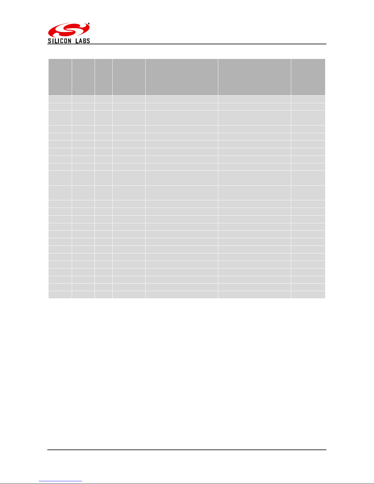
8 ETRX357 pinout
The functions of each of the ETRX357 pins depend on the firmware. When using the Telegesis AT
command-based firmware the S-register settings control the configuration of the I/Os. Some of them
have a main function and an alternate function, as determined by the value of register S15. Holding
pad PA5 low when powering up or resetting the module will cause it to enter the bootloader mode;
this operation lies outside the normal firmware so it is independent of the value of S15. As the
functions are firmware-dependent and may change between versions, Table 3 should be read in
conjunction with the latest R3xx AT Command Manual.
Notes on Table 3 headings
Name is the designation of both the ETRX357 pad and the EM357 chip pin.
Index can be used to reference the individual pin in various S-registers (see the R3xx AT Command
Manual)
Pad is the module’s pad numbering
Default direction indicates whether the pad is normally an input or output
Main function and Alternate function indicate the purpose and connection of the pad
Default alt fn setting indicates whether the default firmware setting chooses the main or alternate
function
Page 9
ETRX357 Development Kit
©2016 Silicon Labs - 9 - ETRX357DVK Product Manual (Rev 1.12)
Name
Index
Pad
Default
direction
S17=
0142CC
Main function
Alternate function
Default
alt fn
setting
S15=
00000600
PC7
17 4 In
PC6
16 3 In
PC5
15 2 In
Enable TX_active on
ETRX357 {4}
PC4
14
24
In
PC3
13
23
In
PC2
12
22
In
PC1
11
26
In ADC3 (light sensor) {2}
PC0
10
27
Out
LED
PB7
F
28
In ADC2, PWM {2}
PB6
E
29
Out
LED, Button 4, IRQ3
{1}
ADC1 {2}
PB5
D
30
In
ADC0 (temp sensor)
{2} PB4
C 8 In
PB3
B 6 In
PB2
A
18
In RXD
Enabled
PB1
9
17
Out TXD
Enabled
PB0
8
25
In
Button 3, IRQ2 {1}
PA7
7 5 Out
LED
PA6
6
16
Out
LED
PA5
5
15
In
(Bootload)
PA4
4
14
In
PA3
3
12
Out
Sensor supply {3}
PA2
2
11
Out
Sensor supply {3}
PA1
1
10
In
Button 2, IRQ1 {1}
PA0
0 9 In
Button 1, IRQ0 {1}
Table 3. Module pads and functions
Notes
{1} The IRQS are always enabled; it is not necessary to activate the alternate function. PB0 is not
available for use on an ETRX357-LRS module as it is used internally to control the RF front-end
module
{2} The ADCs are normally disabled; it is necessary to activate the alternate function
{3} In a development kit, the sensor supply outputs PA2 and PA3 must be high for the sensors to
function
{4} On the ETRX357 TX_active is an output which indicates that the RF circuit is transmitting. On
the ETRX357-LRS TX_active is always selected, and is not available as an ordinary I/O because it
is connected internally to RF components.
Page 10
ETRX357 Development Kit
©2016 Silicon Labs - 10 - ETRX357DVK Product Manual (Rev 1.12)
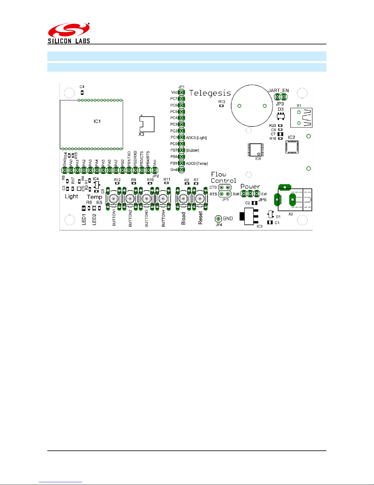
9 The Development Board
9.1 Development Board Interface Description
Figure 4. The development board
Figure 4 shows the location of the connectors described below.
Programming Connector: The 10-way programming connector X3 is used to program the
ETRX357 module from a Silicon Labs InSight Adaptor. It is duplicated on the carrier board, and will
not normally be fitted in the Development Board.
USB Port: The USB serial port allows connectivity to a PC. This provides access to the command
line interface and the bootloader for firmware upgrades, and supplies DC power to the board.
I/O connection: JP1 and JP2 can be used to connect the I/O pins as shown in Table 4.
Reference Ground: JP4 is connected to the devboard’s ground plane. It can be used as a reference
point when making measurements on the devboard.
Page 11
ETRX357 Development Kit
©2016 Silicon Labs - 11 - ETRX357DVK Product Manual (Rev 1.12)
I/O breakout:
JP1 and JP2 give access to the I/O on the ETRX357 module. The individual pins are labelled on the
circuit board, and the pin numbering (PA0, PB1 etc) matches that of the EM357 chip inside the
module.
Pin
Devboard functionality
PA0
Button1
PA1
Button2
PA2
Temp sensor supply
PA3
Light sensor supply
PA5
Bootloader button
PB0
Button3
PB1
TXD
PB2
RXD
PB3
CTS
PB4
RTS
PB5
ADC0 (Temp sensor reading)
PB6
Button4
PB6
LED1
PB7
Buzzer
PC0
LED2
PC1
ADC3 (Light sensor reading)
Table 4. I/O Connectivity on development board
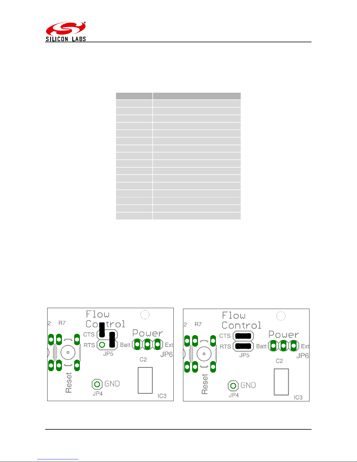
Flow Control Selection: JP5 is used to connect the RTS and CTS lines used for the flow control to
the host. By default flow control is disabled and the corresponding lines of the module are used as
standard I/Os (see the AT command dictionary on how to enable flow control), so the default setting
of JP5 does not connect those lines to the host as shown in Figure 5. When flow control is enabled
JP5 must be set as shown in Figure 6. Please make sure the jumpers are only set to this
configuration when flow control is enabled as otherwise I/Os driving against each other (via a
protective resistor) will increase the current consumption.
Figure 5. No Flow Control (default)
Figure 6. Flow control enabled
Page 12

ETRX357 Development Kit
©2016 Silicon Labs - 12 - ETRX357DVK Product Manual (Rev 1.12)
Power supply jumpers: links must be inserted at JP3 and JP6 according to the DC supply feed.
JP3 can be left connected at all time, but it disconnects the serial interface lines and prevents power
drain through them when the serial (USB) interface is not used. This will minimise the current drain
from a battery and produce a more accurate reading of the current consumption.
It permissible to attach a USB connection while the board is powered from a battery or external
supply.
There are three options:
USB power
External power through the X2
socket
Battery power
Insert JP3. Connect the centre
pin of JP6 to ‘Ext’.
Optionally, omit JP3. Connect
the centre pin of JP6 to ‘Ext’.
Optionally, omit JP3. Connect
the centre pin of JP6 to ‘Batt’.
Figure 7. Power feed options
Instead of a shorting link, a current meter can be inserted at JP6 to monitor the power consumption.
9.2 Development Board Sensors
The board’s temperature sensor IC4 is a National Semiconductor LM61 which has an offset of
600mV and a sensitivity of 10mV/deg. Hence for example 0°C give 600mV and 20° gives 800mV.
The ETRX357’s ADCs have a sensitivity of 0.1mV/LSB, so 100 LSB’s 1 degree.
The light sensor IC5 is an Avago APDS 9005; it indicates ambient light level but is not suitable for
accurate measurements.
Page 13

ETRX357 Development Kit
©2016 Silicon Labs - 13 - ETRX357DVK Product Manual (Rev 1.12)
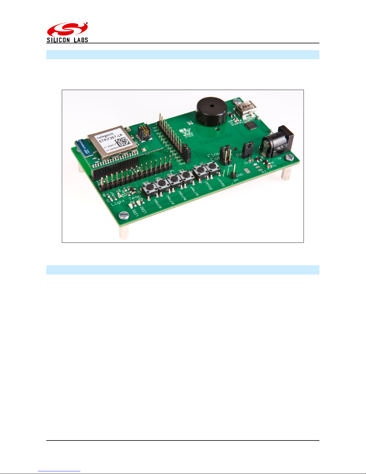
10 The Carrier Board
Figure 8. The carrier board
The ETRX357 carrier board has two LEDs.
Pin
Carrier board functionality
PA6
LED1
PA7
LED2
Table 5. Carrier board LEDs
Programming Connector: The 10-way programming connector X4 is used to program the
ETRX357 module from a Silicon Labs InSight Adaptor.
Watch crystal: an optional 32kHz crystal and its associated capacitors can be fitted at X3, C1 and
C2. In this case, R14 and R15 should be removed from the main development board. The use of
this crystal is dependent on the user’s firmware and the latest Silicon Labs documentation should be
consulted for details of the circuit design.
11 Driver Installation and Operation
The USB drivers obtainable from www.silabs.com/telegesissoftware will generate a virtual COM port
allowing easy access to the serial port of the embedded ETRX357. The ETRX357 development
board uses the same USB-to-serial device as the ETRX2USB and ETRX3USB products, so the
same USB drivers can be used. The development kit board and the USB stick use the same drivers
so you only need to install them once.
11.1 Windows 9x/XP/2k Driver Installation
Install the drivers before connecting the development kit using the provided USB cable. The driver
package should be unzipped into a local folder. When executing the file ‘TGvcpInstaller_x86.exe’ or
‘TGvcpInstaller_x64.exe’ an installer will guide you through the steps required for the driver
installation. Note that updates to the driver package may result in the various messages differing
from the screen-shots shown here.
The installer will first ask you to confirm the location for the files:
Page 14

ETRX357 Development Kit
©2016 Silicon Labs - 14 - ETRX357DVK Product Manual (Rev 1.12)
Figure 9. File location
After the files are installed you may have to restart the computer:
Figure 10. Request to restart
After you connect the devboard Windows® will prompt that new hardware has been found. If you
have not run ‘TGvcpInstaller_xx.exe’ you will have to manually point to the directory into which you
have unzipped the driver. Depending on your PC setup Windows may ask to check the internet for
updated drivers, but there is no point in doing this.
Figure 11. Found New Hardware Wizard
Page 15

ETRX357 Development Kit
©2016 Silicon Labs - 15 - ETRX357DVK Product Manual (Rev 1.12)
Figure 12. Satisfactory completion
Please note that each devboard and USB stick has a unique serial number which requires the
installation procedure to be repeated with every new unit being attached to the computer. This allows
multiple devices to be used on the same computer at any one time. If a USB stick is unplugged and
re-inserted the computer recognises it without having to repeat the installation process, and the USB
device retains its former COM port number.
In order to find out the identity/number of the virtual COM port the devboard or USB stick has been
assigned to, please open the Device Manager under the Windows Computer Management screen
(see below) and click on the Ports (COM and LPT) section where you should find the new virtual
COM port. By double clicking on the entry of the virtual COM port you can also change the number
assigned to the virtual COM port when entering the advanced setup of the device.
Page 16

ETRX357 Development Kit
©2016 Silicon Labs - 16 - ETRX357DVK Product Manual (Rev 1.12)
Figure 13. Device Manager
Once the correct COM port has been selected, the Telegesis Terminal software can be used to
control the devboard as described in chapter 11.
Figure 14. Telegesis Terminal
Page 17

ETRX357 Development Kit
©2016 Silicon Labs - 17 - ETRX357DVK Product Manual (Rev 1.12)
12 Application Software
The command line of the ETRX357 can be accessed using any terminal software program such as
HyperTerminal®. Simply set up HyperTerminal® to connect to the appropriate COM port at
19200bps, Data bits - 8, Parity - none, Stop bits - 1, Flow Control – none (ETRX357 factory default).
To speed up evaluation Telegesis provides its own Terminal Application Software program which
allows enhanced functionality especially suited to the ETRX357 modules. The AT-Style commands
can be issued by clicking on customisable ‘Command’ buttons and all of the 64-bit serial numbers
which report are listed in a separate window. This means you will not need to input any of the 64-bit
serial numbers.
For instructions on how to use the AT commands read the R3xx AT Command Manual.
Note: Telegesis Terminal does not interpret the AT commands and send instructions to the ETRX357
in a different format. It does not alter the AT commands in any way – the ETRX357 receives them
exactly as described here and in the AT Command Manual. Likewise, if you are writing your own
terminal application, it should send and receive data as formatted in our manuals.
Figure 15. Appearance of the Telegesis Terminal Application Software
Page 18

ETRX357 Development Kit
©2016 Silicon Labs - 18 - ETRX357DVK Product Manual (Rev 1.12)
12.1 Software Set-up
Telegesis Terminal R4.0 no longer needs .NET Framework Version 1.1 which was required for earlier
versions. Download Telegesis Terminal from our website at
www.silabs.com/telegesissoftware
With recent operating systems such as Windows 7, it is advisable to right-click on the Telegesis
Terminal setup program and select “Run as administrator”. This avoids problems when you try to
save customised button layout files as they are normally stored in the program folders.
After installing and starting the Telegesis Terminal Application program a single command button for
the firmware will be shown at the bottom of the window. In order to use the Telegesis Terminal
software, first open the correct button layout file for your firmware by selecting File Open Layout,
then select the correct COM port and the connection parameters (ETRX357 default 19200, 8 bits,
no parity, no flow control) and press the connect button. These settings are automatically retained
each time the software is re-started.
12.2 Features of the Telegesis Terminal Application for ETRX357
The buttons
To make life easy many of the AT commands have been pre-defined and conveniently grouped at
the bottom of the terminal window. Pressing a button (where no parameters are required) causes
the corresponding command to be issued instantly. Where a parameter is required the command is
shown in the Command bar and the required parameter can be entered manually. In order to issue
the command from the command bar simply press the <enter> or the Send button. To see the
parameters for a specific command, move and hold the mouse pointer over the chosen command
button - Figure 16.
Figure 16. Screen tips for parameters
The application software also allows you to add custom command buttons and edit existing
command buttons. New groups of commands can be created and command buttons can be moved
between groups.
The device window
Every EUI64 number reporting in is listed in a separate window which can be opened or closed by
clicking on the button labelled ‘Device List’. If a device ID is required as a parameter in the command
bar, simply double click on an entry in the device list and its EUI64 will be automatically transferred
to the current cursor position of the command bar.
Page 19

ETRX357 Development Kit
©2016 Silicon Labs - 19 - ETRX357DVK Product Manual (Rev 1.12)
To allow for easier identification, the EUI64 IDs in the device list can be named. When right clicking
on any EUI64 ID a name can be associated with the respective ID - Figure 17.
Figure 17. Device Naming
The menu bar
Figure 18. Telegesis Terminal menu bar
File To open and save button layout files
Connection To switch connection address mode between COM port and IP address
Commands To open a button layout editor
Log To save a record of the session
Tools Refresh COM Ports – update the drop-down list of ports
Transfer File – open an XMODEM dialogue window
Send Text – import a file into the large dialogue window
Show STX ETX – displays <stx> and <etx> characters when the firmware
uses them to bracket its output
Use Nonprinting Characters – characters can be entered as two
hexadecimal characters bracketed by <…>, eg <41> for A or <0D> for
carriage return
Help Shows the software version
Button layout files are normally found in the folder into which Telegesis Terminal was installed. They
are xml files so they can be edited by a text editor or by a tool such as the Microsoft XML Notepad,
as well as from within Telegesis Terminal itself. Buttons usually have a single AT command attached
to them, but v4 of Telegesis Terminal allows a button to have multiple commands, each terminated
by <cr>. When the button is pressed a 100ms delay is inserted after each command.
Connection can be made to a COM port or to an IP address and port number; the latter opens a TCP
connection.
Page 20

ETRX357 Development Kit
©2016 Silicon Labs - 20 - ETRX357DVK Product Manual (Rev 1.12)
XMODEM is generally used when bootloading a new firmware file on to a module.
12.3 A Quick Start
This section gives you a quick introduction on how to get started. Power up the node connected to
the PC and open a connection to the correct device; refresh the list of COM ports if the expected
device is not shown. Type AT followed by <enter>. If the communication to the module is working
the module will prompt OK, if not check the USB connectivity and driver status and make sure you
have connected to the correct COM port with the correct speed. Please note that even when
connected to the wrong COM port there may be a reply to AT, for example when you are
communicating with your PC’s modem or Bluetooth device. To double check you are actually
communicating with a Telegesis ZigBee device use the ATI command described below.
Select the correct set of buttons
Type ATI<enter> to verify your firmware version (eg R308C). Then select File Open Layout on
the menu bar and open the appropriate xml file – usually R3xx.xml. This attaches the correct set of
AT commands to the buttons. You can create your own button configurations for different situations
and save them as separate files. Telegesis Terminal starts up using the configuration of the previous
session.
Network Setup
Figure 19. Command Line Interactions
To establish a PAN network issue the
AT+EN command, or alternatively
press the ‘Establish PAN’ button.
The local unit will now scan all
available 16 channels and establish a
PAN with a random PAN ID, on the
quietest available one. This may take
up to 16 seconds and leads to the
node becoming the network’s
coordinator. When successful the
module will prompt ‘JPAN’ followed by
the details of the newly created PAN.
If you get an error message instead, it
is likely that the module was already
part of a PAN, so you will need to
issue the AT+DASSL command or
press the ‘Disas Local’ button to
leave the PAN before going back to
starting a new one. In order to find out
about the network status simply issue
the AT+N command or press the
‘NWK Info’ button.
Once the network is established, remote nodes can be powered up ready to join in. If you have
serial access to remote nodes simply issue the AT+JN command or press the ‘Join any PAN’ button,
to join the newly established PAN. If you do not have serial access to the remote nodes (as is the
Page 21

ETRX357 Development Kit
©2016 Silicon Labs - 21 - ETRX357DVK Product Manual (Rev 1.12)
case of the two MCBs provided with the previous ETRX2-based DVKA) you will just need to wait for
them to join the network automatically. By default, once every minute all nodes (except coordinators)
are set up to check whether there are any neighbours on the same PAN nearby, or if they have been
orphaned. If no neighbours are found after 5 consecutive tries, the unit will leave the (deserted) PAN
and then try to join a new one once every minute.
This initial network set-up can take a few minutes, especially with no serial access to remote nodes,
but once the network is set up it will remain set even after power cycles. New nodes joining will
cause a prompt ‘NEWNODE:’ on the remote side and display the JPAN message locally as
described above.
The ETRX357 stores its network parameters in non-volatile memory, so if you reset or power-cycle
a module there is no need to re-establish or join the PAN again.
If devices do not join the desired PAN automatically, check that they are not already in a network of
their own. The command AT+PANSCAN will reveal the presence of other networks in the vicinity.
To learn more about setting up and maintaining a PAN please refer to the user guide and the AT
Command Dictionary.
Mesh networking
A typical ZigBee network is a mesh, where every device can send a message to any other device.
If the two devices are in radio range of each other the message passes directly, but if they are too
far apart the message is relayed via an intermediate device. The routing is taken care of by the
firmware and the user is generally not even aware that it is happening. You can easily discover the
basic principles of mesh networking: simply move a Development Board out of range (if you do not
have enough space simply turn the transmit power down or put it behind a metal screen) and then
add another Development Board between the local node and the remote one. You will find that the
network has healed the broken link and all three nodes are accessible again.
Node types
A ZigBee node is one of several types:
Router. If you have started a network as described so far in this manual, all the devices are
routers and can communicate directly with each other
Coordinator. This is merely the device which first established the network. It is also the trust
centre which grants permission for other devices to join, so do not disassociate it from your
network
Sleepy End Device. SEDs do not play any part in the routing so they can be put into a sleep
state while they do not need to send or receive messages. To turn a device into an SED
disassociate it from your network, set bit E of register S0A with the command
ATS0AE=1;password then let it join the network. An SED is adopted by a parent router which
buffers any messages sent to the SED until it sends a Data Request (or poll) to its parent to
indicate it is ready to receive. The power mode is defined in register S39, so refer to the AT
command manual for more details
Mobile End Device. MEDs are like SEDs but they react more quickly when they move of range
of their parent and need to find a new one. Set bits E and F of register S0A to create an MED
ZigBee End Device. ZEDs cannot be put into a sleep state to save power nor do they take part
in the routing, so they are of very limited use
Page 22

ETRX357 Development Kit
©2016 Silicon Labs - 22 - ETRX357DVK Product Manual (Rev 1.12)
12.4 Configuring Buttons for your Setup
You can open several copies of Telegesis Terminal on the same PC, so if you have two or more
development boards connected to a PC try sending messages between them using the Broadcast
or Unicast buttons. This will begin to give you an understanding on how to integrate the ETRX357
into your application. The Telegesis Terminal Application also allows you to create custom command
buttons for your individual application, just click on Commands / Add command button.
Figure 20. Button editor
In this way you can add buttons that are specific to your tests, reduce the number of buttons to a
simple layout for demonstrations, or create a sequence of operations for commissioning devices and
systems.
The first button on the pre-supplied layouts is . When you click on this, the local
device executes the AT+SN command to scan the network for other devices and for each one it adds
three new buttons:
, (in the Send Data – R3xx group)
(in the Register Access – R3xx group).
Clicking any of these controls the LEDs on the corresponding dev board, or sounds its buzzer.
For a more detailed description of the AT command interface please refer to the appropriate
command manual for your version of firmware R3xx.
Some useful I/O commands for the ETRX357 are given in the next section.
Configure
LEDS n ON
LEDS n OFF
Ident Noden
Page 23

ETRX357 Development Kit
©2016 Silicon Labs - 23 - ETRX357DVK Product Manual (Rev 1.12)
12.5 Using LEDs and ADCs on the ETRX357
The LEDs are connected to the ETRX357 in a pull-down arrangement so each output must be set
to ‘0’ to turn on its LED. Refer to Table 3 for details of the various connections; since they are
distributed across the 16 I/O pins some examples of typical functions are given here for convenience.
The four LED pins are configured as outputs by default so they can be used immediately. Before
each ADC can be used, its pin must be set to use the alternate function in register S15, but it does
not matter whether it is defined as a digital input or output. The temperature and light sensors on
the circuit board are powered from two of the ETRX357’s outputs, so these pins must be set high in
order for the sensors to function.
Turn on local LEDs
ATS18=00000000
Turn off local LEDs
ATS18=000140C0
Turn off LEDs at EUI64 000D6F0000D5ED27
ATREMS:000D6F0000D5ED27,18=000140C0
Turn off all remote LEDs in the network
ATSALL,FFFF,18=000140C0
Turn on local LEDs and supply power to
temperature and light sensors
ATS18=0000000C
Enable temperature and light ADCs
ATS15=0002E600
Read local light sensor
ATS22?
Note that these immediately change the actual values of the registers described but not their default
values.
The ADC registers can be read on a local or remote device by using the ATS or ATREMS commands,
but they can also be sent automatically to the network sink by using function 0110 or 0130; consult
the AT Command Manual for the details, and see section 12.6 here.
Page 24

ETRX357 Development Kit
©2016 Silicon Labs - 24 - ETRX357DVK Product Manual (Rev 1.12)
12.6 Temperature display
The AT command set provides two powerful features:
1. A node can be defined as a “sink”. It broadcasts its address to the rest of the network, so the
other devices can use commands and built-in functions that send data to the sink. In this way, an
application can be designed without the need to know in advance the address of the sink node, which
will be different in each installation.
2. Software timers implemented in the firmware can execute various predefined functions. Simple
applications can therefore often be implemented without the need for a host processor to send AT
commands to a device.
As an example of both of these features, the following commands demonstrate how to collect
temperature information from development kit boards:
1. Define the module on the data-gathering development board as the network sink with the
command
ATS104=1
2. Instruct one or more sensor development boards to send their ADC readings to the sink at
regular intervals by setting a Timer/Counter on the ETRX357, eg to send every second
using Timer/Counter 5 use these commands on each sensor board:
ATS33=0004
ATS34=8130
3. Activate all four ADCs on each sensor board with the command
ATS15=0002E600
4. Turn on the sensor power on each sensor board with the commands
ATS182=1
ATS183=1
5. The ADC readings will appear at the sink in the form of a “FN130” prompt, which also
contains the digital I/O values and the contents of the S46 counter register. See the AT
Command Manual for full details of the prompt and the registers used here. The units are
0.1mV; the sensor has a slope of 10mV/deg with a 600mV offset.
It is usually easiest to set the sensor device’s registers by accessing them via USB, but you can also
use the ATREMS command from the sink node.
Page 25

ETRX357 Development Kit
©2016 Silicon Labs - 25 - ETRX357DVK Product Manual (Rev 1.12)
13 Firmware upgrades
If required, the firmware of the ETRX357 modules can be upgraded serially as well as over the air.
Over-the-air upgrading is primarily a function of the Silicon Labs bootloader and it is not available
with the early bootloader versions. See section 13.2 for more details.
13.1 Firmware Upgrades via Serial Port
In order to upgrade the firmware of the ETRX357 module using the serial bootloader, issue the
“AT+BLOAD” command either by typing it in, or by pressing the respective button in the “Module
Control” group of the Telegesis Terminal Application.
Alternatively the button labelled “Bload” can be pressed on the development board whilst the reset
button is pressed and released.
After entering the bootloader, the connection parameters need to be changed to 115200bps, 8 data
bits, 1 stop bit, no parity, no flow control (providing that it is not already set to these values).
After pressing ‘Enter’, the bootloader menu will be shown in the terminal window as shown in Figure
21.
Figure 21. Bootloader Menu
Pressing ‘1’ initiates the upload of the new firmware and a number of ‘C’ characters will indicate that
the ETRX357 is ready to receive data. Within 60 seconds, select Tools / Transfer File… and browse
for the new firmware file.
Firmware files for the ETRX357 will be in the format ETRX357_R3xxC.ebl. After checking that the
protocol is set to XMODEM (128 Bytes), press the Send button and the new firmware will be
downloaded as shown in Figure 22.
Page 26

ETRX357 Development Kit
©2016 Silicon Labs - 26 - ETRX357DVK Product Manual (Rev 1.12)
Figure 22. File Transfer Window
When the transfer has been completed successfully, press Enter again in order to return to the
bootloader menu (shown in Figure 21) and option ‘2‘ to run the downloaded application software. If
the application software has a baudrate other than 115200bps, this will need to be changed to the
application baudrate as described above – 19200 baud in the case of R3xx firmware.
Page 27

ETRX357 Development Kit
©2016 Silicon Labs - 27 - ETRX357DVK Product Manual (Rev 1.12)
13.2 Over the Air Firmware Upgrades
ETRX2 and ETRX357 features
With the ETRX2, upgrading over the air is possible by cloning a local node’s firmware to a remote
node, so if new firmware has to be introduced to the network it can be downloaded serially to a
master node, which then can clone itself to one node after the other in turn given the target node is
only a single hop away. Cloning between some firmware releases may not always be possible, so
check the Firmware Revision History for relevant comments.
The ETRX357 uses passthrough OTA bootloading, so the new file is stored in the host processor
and loaded on to the target device by transmitting it through the local device. The local device is
therefore not required to have the same firmware as the updated target.
The ETRX2 and ETRX357 have different bootloaders and firmware files as well as different modes
of transferring the new file. Consequently you cannot upgrade an ETRX357 via an ETRX2 or viceversa.
Passthrough with an ETRX357
You should first verify that the module’s bootloaders are sufficiently recent, as this feature was not
included in the earliest versions. Start the bootloader with the AT+BLOAD command, enter a <cr>
and check the response, then exit the bootloader without altering the firmware by selecting option 2
(‘run’). The bootloader needs to be version v42 or higher for passthrough to be possible, or else v01
which is a Telegesis variant of the Silicon Labs bootloader. A new bootloader can only be installed
by reflashing the module’s memory with a Silicon Labs Insight Adaptor.
The passthrough process is similar to bootloading a file on to the local device, except that there is
no need to change the baud rate. Use the command
AT+PASSTHROUGH:<EUI64 of the target device>:<Target device’s password>
The device will respond with a prompt and a sequence of ‘C’ characters. Select Tools / Transfer
File… from the drop-down menu of Telegesis Terminal and browse for the new firmware file.
Firmware files for the ETRX357 will be in the format ETRX357_R3xxC.ebl. After checking that the
protocol is set to XMODEM (128 Bytes), press the Send button and the new firmware will be
downloaded as shown in Figure 22.
Passthrough bootloading on to an End Device or across multiple hops is not possible.
Page 28

ETRX357 Development Kit
©2016 Silicon Labs - 28 - ETRX357DVK Product Manual (Rev 1.12)
Figure 23. Passthrough bootloading
Recovering on the default channel
If the target device is reset or power cycled whilst in the bootloader, the unit will listen for new
firmware files on channel 13. It is therefore required to set up a node on channel 13 and repeat the
recovery action described in the previous section.
To set up a node on channel 13 use the following commands:
AT+DASSL – leave the current network (will show an error if not currently part of a network)
ATS00=0004 – Only allow channel 13
AT+EN – establish new network on channel 13
This will cause the local node to become a coordinator on channel 13.
AT+RECOVER
The local node will search for a remote node in bootload mode and clone the local firmware to that
remote node.
Page 29

ETRX357 Development Kit
©2016 Silicon Labs - 29 - ETRX357DVK Product Manual (Rev 1.12)
14 Hardware enhancement kit
For users who are developing their own firmware on the Silicon Labs EM3587 chip, Telegesis offer
an enhancement pack for the ETRX357 Development Kit or the Silicon Labs EM35x Development
Kit that contains EM3587-based modules on carrier boards. This will enable you to download your
application to the modules and verify its operation on our development kit boards. In this way you
can demonstrate that your firmware is portable on to the ETRX3587, that it functions correctly with
the power amplifier of the ETRX3587-LRS, and that it is over-the-air compatible with the ETRX357.
Each enhancement pack contains two examples of the following, each on a carrier board:
Model
Antenna
Max RF power
ETRX3587
Antenova Rufa
8dBm
ETRX3587HR
Hirose U.FL connector for external antenna
8dBm
ETRX3587-LRS
Antenova Rufa
20dBm
ETRX3587HR-LRS
Hirose U.FL connector for external antenna
20dBm
Table 6. ETRX3587 Enhancement Pack contents
The devices in the enhancement pack will be supplied with the Silicon Labs nodetest firmware.
Connect to the COM port of the board at 115200 baud and type help, which returns a list of the
available commands. There is some information about the commands in the SiLabs application note
AN710 Bringing Up Custom Devices For The Ember® Em35x Soc Platform at
www.silabs.com/support/pages/document-library.aspx?p=Wireless&f=ZigBee&pn=EM357
but the command set is otherwise undocumented.
Page 30

ETRX357 Development Kit
©2016 Silicon Labs - 30 - ETRX357DVK Product Manual (Rev 1.12)
15 Devboard Schematic
Page 31

ETRX357 Development Kit
©2016 Silicon Labs - 31 - ETRX357DVK Product Manual (Rev 1.12)
Page 32

ETRX357 Development Kit
©2016 Silicon Labs - 32 - ETRX357DVK Product Manual (Rev 1.12)
16 Carrier Board Schematic
Page 33

ETRX357 Development Kit
©2016 Silicon Labs - 33 - ETRX357DVK Product Manual (Rev 1.12)
17 ETRX357 Ordering Information
Ordering/Product Code
Description
ETRX357
Telegesis Wireless Mesh Networking Module with Silicon Labs
ZigBee® Technology:
Telegesis AT Style Command Interpreter based on
Silicon Labs’ EmberZNet stack
Integrated 2.4GHz Antenna
ETRX357HR
Telegesis Wireless Mesh Networking Module with Silicon Labs
ZigBee® Technology:
Telegesis AT Style Command Interpreter based on
Silicon Labs’ EmberZNet stack
Hirose U.FL Antenna Connector
ETRX357DVK
Telegesis Development Kit with:
3 x ETRX357DV Development Boards
2 x ETRX357 Modules on Carrier Boards
2 x ETRX357HR Modules on Carrier Boards
2 x ETRX357-LRS Modules on Carrier Boards
2 x ETRX357HR-LRS Modules on Carrier Boards
1 x ETRX3USB stick
2 x ½-wave antennae
2 x ¼-wave antennae
3 x USB Cables
ETRX3587 Enhancement Pack
2 x ETRX3587 Modules on Carrier Boards
2 x ETRX3587HR Modules on Carrier Boards
2 x ETRX3587-LRS Modules on Carrier Boards
2 x ETRX3587HR-LRS Modules on Carrier Boards
Notes:
Customers’ PO’s must state the Ordering/Product Code.
There is no “blank” version of the ETRX357 Module available. All Modules carry the
Telegesis AT style Command Layer based on the EmberZNet Stack. (Where customers
wish to add their own firmware they can re-program the flash memory of the embedded
EM357).
Please contact Telegesis if you require additional AT style commands or specific integration
assistance.
Page 34

Smart.
Connected.
Energy-Friendly
Products
www.silabs.com/products
Disclaimer
Silicon Laboratories intends to provide customers with the latest, accurate, and in-depth documentation of all peripherals and modules available for system and software implementers using
or intending to use the Silicon Laboratories products. Characterization data, available modules and peripherals, memory sizes and memory addresses refer to each specific device, and
"Typical" parameters provided can and do vary in different applications. Application examples described herein are for illustrative purposes only. Silicon Laboratories reserves the right to
make changes without further notice and limitation to product information, specifications, and descriptions herein, and does not give warranties as to the accuracy or completeness of the
included information. Silicon Laboratories shall have no liability for the consequences of use of the information supplied herein. This document does not imply or express copyright licenses
granted hereunder to design or fabricate any integrated circuits. The products are not designed or authorized to be used within any Life Support System without the specific written consent
of Silicon Laboratories. A "Life Support System" is any product or system intended to support or sustain life and/or health, which, if it fails, can be reasonably expected to result in significant
personal injury or death. Silicon Laboratories products are not designed or authorized for military applications. Silicon Laboratories products shall under no circumstances be used in
weapons of mass destruction including (but not limited to) nuclear, biological or chemical weapons, or missiles capable of delivering such weapons.
Trademark Information
Silicon Laboratories Inc.® , Silicon Laboratories®, Silicon Labs®, SiLabs® and the Silicon Labs logo®, Bluegiga®, Bluegiga Logo®, Clockbuilder®, CMEMS®, DSPLL®, EFM®, EFM32®,
EFR, Ember®, Energy Micro, Energy Micro logo and combinations thereof, "the world’s most energy friendly microcontrollers", Ember®, EZLink®, EZRadio®, EZRadioPRO®, Gecko®,
ISOmodem®, Precision32®, ProSLIC®, Simplicity Studio®, SiPHY®, Telegesis, the Telegesis Logo®, USBXpress® and others are trademarks or registered trademarks of Silicon Laboratories Inc. ARM, CORTEX, Cortex-M3 and THUMB are trademarks or registered trademarks of ARM Holdings. Keil is a registered trademark of ARM Limited. All other products or brand
names mentioned herein are trademarks of their respective holders.
Silicon Laboratories Inc.
400 West Cesar Chavez
Austin, TX 78701
USA
Quality
www.silabs.com/quality
Support and Community
community.silabs.com
http://www.silabs.com
 Loading...