

Silicon Laboratories SiM3U1xx, SiM3U1x7, SiM3U1x6, SiM3U1x4 User Manual

SiM3U1xx
High-Performance, Low-Power, 32-Bit Precision32™
USB MCU Family with up to 256 kB of Flash
32-bit ARM® Cortex™-M3 CPU
- 80 MHz maximum frequency
- Single-cycle multiplication, hardware division support
- Nested vectored interrupt control (NVIC) with 16 levels of
interrupt priority
Memory
- 32–256 kB Flash, in-system programmable
- 8–32 kB SRAM (including 4 kB retention SRAM)
- External bus interface supports up to 16 MB of external mem-
ory and a parallel LCD interface with QVGA resolution
Power Management
- Low drop-out (LDO) regulator
- Power-on reset circuit and brownout detectors
- 5-to-3.3 V voltage regulator supports up to 150 mA to drive the
device directly from USB; no off-chip regulator required
- Programmable external regulator supports up to 3.6 V,
mA
1000
- Multiple power modes supported for low power optimization
Clock Sources
- Internal oscillator with PLL: Fine frequency resolution up to
80
MHz; spread-spectrum mode for reduced EMI
- USB internal 48 MHz oscillator supports crystal-less operation
- Low power internal oscillator: 20 MHz and 2.5 MHz modes
- Low frequency internal oscillator: 16.4 kHz
- External oscillators: Crystal, RC, C, CMOS and RTC Crystal
- Flexible clock divider: Reduce frequency by up to 128x from
any clock source
128/192/256-bit Hardware AES Encryption
- Hardware-supported Electronic Codebook (ECB), Cipher-Block
Chaining (CBC) and Counter (CTR) algorithms
- All cipher operations can be performed without any firmware
intervention for a set of 4-word blocks (up to 32
kB)
16/32-bit CRC
- Hardware support for common 32-bit and 16-bit polynomials
Timers/Counters
- 2 x 32-bit or 4 x 16-bit timers with capture/compare
- 2 x 16-bit, 2-channel counters with capture/compare/PWM
- 16-bit, 6-channel counter with capture/compare/PWM and
dead-time controller with differential outputs
- 16-bit low power timer/pulse counter operational in the lowest
power mode
- 32-bit real time clock (RTC) with multiple alarms
- Watchdog timer
Current-to-Voltage Converter
- Supports up to 6 mA input range
Supply Voltage
- 2.7 to 5.5 V (regulator enabled)
- 1.8 to 3.6 V (regulator disabled)
Low Power Features
- 85 nA current mode with voltage supply monitor enabled
- 350 nA current mode with RTC (internal oscillator)
- 620 nA current mode with RTC (external oscillator)
- 10 µs wakeup (lowest power mode); 1.5 µs analog setting time
- 275 µA/MHz active current
- Clocks can be gated off from unused peripherals to save power
2 x 12-Bit Analog-to-Digital Converters
- Up to 28 input channels
- Up to 250 ksps 12-bit mode or 1 Msps 10-bit mode
- Single, simultaneous, and interleaving modes supported
- Channel sequencer enables automatic multiplexing of multiple
channels without firmware intervention
- Internal VREF or external VREF supported
2 x 10-Bit Digital-to-Analog Converters
- DMA support for waveform generation
- Four-word circular buffer to enable 12-bit mode
16-Channel Capacitance-to-Digital Converter
- Supports buttons, sliders, wheels, and capacitive proximity
- Fast conversion time; <1 µA wake-on-touch average current
Two Low-Current Comparators
- Integrated 6-bit programmable reference voltage
- 400 nA current consumption in low power mode
16-Channel DMA Controller
- Supports ADC, DAC, USB, I2C, I
capacitive sensing, external triggers, and timers
2
S, SPI, USART, AES, EPCA,
Up to 65 Flexible I/O
- Up to 59 contiguous GPIO with two priority crossbars providing
flexibility in pin assignments; 12 x 5
V tolerant GPIO
- Up to 6 programmable high drive capable (5–300 mA, 1.8–6 V)
I/O can drive LEDs, power MOSFETs, buzzers, etc.
Communication Interfaces
- USB 2.0-compliant full speed with 10 endpoints, 2 kB buffer,
oscillator with automatic frequency correction, and transceiver;
no external components needed
- 2 x USARTs and 2 x UARTs with IrDA and ISO7816 SmartCard
- 3 x SPIs, 2 x I2C, I
2
S (receive and transmit)
On-Chip Debugging
- Serial wire debug (SWD) and JTAG allow for full-speed, non-
intrusive debug
- Serial wire viewer (SWV) available in 64 / 80 / 92-pin packages
- Cortex-M3 embedded trace macrocell (ETM) in 80 / 92-pin
packages
Temperature Range: –40 to +85 °C
Package Options
- QFN options: 40-pin (6 x 6 mm), 64-pin (9 x 9 mm)
- TQFP options: 64-pin (10 x 10 mm), 80-pin (12 x 12 mm)
- LGA option: 92-pin (7 x 7 mm)
Preliminary Rev. 0.8 2/12 Copyright © 2012 by Silicon Laboratories SiM3U1xx
This information applies to a product under development. Its characteristics and specifications are subject to change without notice.

SiM3U1xx
2 Preliminary Rev. 0.8

SiM3U1xx
Table of Contents
1. Related Documents and Conventions...............................................................................5
1.1. Related Documents........................................................................................................5
1.1.1. SiM3U1xx/SiM3C1xx Reference Manual...............................................................5
1.1.2. Hardware Access Layer (HAL) API Description ....................................................5
1.1.3. ARM Cortex-M3 Reference Manual.......................................................................5
1.2. Conventions ...................................................................................................................5
2. Typical Connection Diagrams ............................................................................................6
2.1. Power.............................................................................................................................6
3. Electrical Specifications......................................................................................................9
3.1. Electrical Characteristics................................................................................................9
3.2. Thermal Conditions......................................................................................................33
3.3. Absolute Maximum Ratings..........................................................................................33
4. Precision32™ SiM3U1xx System Overview ....................................................................35
4.1. Power...........................................................................................................................37
4.1.1. LDO and Voltage Regulator (VREG0).................................................................37
4.1.2. Voltage Supply Monitor (VMON0) .......................................................................37
4.1.3. External Regulator (EXTVREG0) ........................................................................37
4.1.4. Power Management Unit (PMU)..........................................................................37
4.1.5. Device Power Modes...........................................................................................38
4.2. I/O.................................................................................................................................40
4.2.1. General Features.................................................................................................40
4.2.2. High Drive Pins (PB4)..........................................................................................40
4.2.3. 5 V Tolerant Pins (PB3).......................................................................................40
4.2.4. Crossbars ............................................................................................................40
4.3. Clocking........................................................................................................................41
4.3.1. PLL (PLL0)...........................................................................................................42
4.3.2. Low Power Oscillator (LPOSC0) .........................................................................42
4.3.3. Low Frequency Oscillator (LFOSC0)...................................................................42
4.3.4. External Oscillators (EXTOSC0)..........................................................................42
4.4. Data Peripherals...........................................................................................................
4.4.1. 16-Channel DMA Controller.................................................................................43
4.4.2. 128/192/256-bit Hardware AES Encryption (AES0) ............................................43
4.4.3. 16/32-bit CRC (CRC0).........................................................................................43
4.5. Counters/Timers and PWM..........................................................................................44
4.5.1. Programmable Counter Array (EPCA0, PCA0, PCA1)........................................44
4.5.2. 32-bit Timer (TIMER0, TIMER1)..........................................................................44
4.5.3. Real-Time Clock (RTC0) .....................................................................................45
4.5.4. Low Power Timer (LPTIMER0)............................................................................45
4.5.5. Watchdog Timer (WDTIMER0)............................................................................45
4.6. Communications Peripherals .......................................................................................46
4.6.1. External Memory Interface (EMIF0).....................................................................46
4.6.2. USB0 ..................................................................................................................46
4.6.3. USART (USART0, USART1)...............................................................................46
4.6.4. UART (UART0, UART1)......................................................................................47
43
Preliminary Rev. 0.8 3

SiM3U1xx
4.6.5. SPI (SPI0, SPI1)..................................................................................................47
4.6.6. I2C (I2C0, I2C1)...................................................................................................47
4.6.7. I2S (I2S0).............................................................................................................48
4.7. Analog..........................................................................................................................49
4.7.1. 12-Bit Analog-to-Digital Converters (SARADC0, SARADC1)..............................49
4.7.2. Sample Sync Generator (SSG0) .........................................................................49
4.7.3. 10-Bit Digital-to-Analog Converter (IDAC0, IDAC1) ............................................49
4.7.4. 16-Channel Capacitance-to-Digital Converter (CAPSENSE0)............................50
4.7.5. Low Current Comparators (CMP0, CMP1)..........................................................50
4.7.6. Current-to-Voltage Converter (IVC0)...................................................................50
4.8. Reset Sources..............................................................................................................51
4.9. Security ........................................................................................................................52
4.10.On-Chip Debugging.....................................................................................................52
5. Pin Definitions and Packaging Information.....................................................................53
5.1. SiM3U1x7 Pin Definitions.............................................................................................53
5.2. SiM3U1x6 Pin Definitions.............................................................................................61
5.3. SiM3U1x4 Pin Definitions.............................................................................................68
6. Ordering Information.........................................................................................................72
6.1. LGA-92 Package Specifications...................................................................................74
6.1.1. LGA-92 Solder Mask Design...............................................................................76
6.1.2. LGA-92 Stencil Design ........................................................................................76
6.1.3. LGA-92 Card Assembly.......................................................................................76
6.2. TQFP-80 Package Specifications ................................................................................77
6.2.1. TQFP-80 Solder Mask Design.............................................................................80
6.2.2. TQFP-80 Stencil Design......................................................................................80
6.2.3. TQFP-80 Card Assembly.....................................................................................80
6.3. QFN-64 Package Specifications ..................................................................................81
6.3.1. QFN-64 Solder Mask Design...............................................................................83
6.3.2. QFN-64 Stencil Design........................................................................................83
6.3.3. QFN-64 Card Assembly.......................................................................................83
6.4. TQFP-64 Package Specifications ................................................................................84
6.4.1. TQFP-64 Solder Mask Design.............................................................................87
6.4.2. TQFP-64 Stencil Design......................................................................................87
6.4.3. TQFP-64 Card Assembly.....................................................................................87
6.5. QFN-40 Package Specifications ..................................................................................88
6.5.1. QFN-40 Solder Mask Design...............................................................................90
6.5.2. QFN-40 Stencil Design........................................................................................90
6.5.3. QFN-40 Card Assembly.......................................................................................90
7. Revision Specific Behavior...............................................................................................91
7.1. Revision Identification ..................................................................................................91
7.2. Comparator Rising/Falling Edge Flags in Debug Mode (CMP0, CMP1)......................92
7.2.1. Problem ...............................................................................................................92
7.2.2. Impacts................................................................................................................92
7.2.3. Workaround.........................................................................................................92
7.2.4. Resolution............................................................................................................92
Contact Information................................................................................................................94
4 Preliminary Rev. 0.8

SiM3U1xx
Internal Module
External Memory
Block
Output_Pin
External to MCU
Block
Input_Pin
Internal_Output_SignalInternal_Input_Signal
REGn_NAME / BIT_NAME
DMA Block Memory Block
Other Internal
Peripheral Block
Functional Block
1. Related Documents and Conventions
1.1. Related Documents
This data sheet accompanies several documents to provide the complete description of the SiM3U1xx device
family.
1.1.1. SiM3U1xx/SiM3C1xx Reference Manual
The Silicon Laboratories SiM3U1xx/SiM3C1xx Reference Manual provides detailed functional descriptions for the
SiM3U1xx devices.
1.1.2. Hardware Access Layer (HAL) API Description
The Silicon Laboratories Hardware Access Layer (HAL) API provides C-language functions to modify and read
each bit in the SiM3U1xx devices. This description can be found in the SiM3xxxx HAL API Reference Manual.
1.1.3. ARM Cortex-M3 Reference Manual
The ARM-specific features like the Nested Vector Interrupt Controller are described in the ARM Cortex-M3
reference documentation. The online reference manual can be found here:
http://infocenter.arm.com/help/topic/com.arm.doc.subset.cortexm.m3/index.html#cortexm3.
1.2. Conventions
The block diagrams in this document use the following formatting conventions:
Figure 1.1. Block Diagram Conventions
Preliminary Rev. 0.8 5

SiM3U1xx
SiM3U1xx Device
VREGn
VREGIN
VSS
VBUS
VSSHD
1 uF and 0.1 uF bypass
capacitors required for
each power pin placed
as close to the pins as
possible.
3.3 V (out)
5 V (in)
VDD
VIO
VIOHD
SiM3U1xx Device
VREGn
VREGIN
VSS
1.8-3.6 V (in)
VBUS
VSSHD
1 uF and 0.1 uF bypass
capacitors required for
each power pin placed
as close to the pins as
possible.
VDD
VIO
VIOHD
2. Typical Connection Diagrams
This section provides typical connection diagrams for SiM3U1xx devices.
2.1. Power
Figure 2.1 shows a typical connection diagram for the power pins of the SiM3U1xx devices when the internal
regulator is in use and USB is not used.
Figure 2.1. Connection Diagram with Voltage Regulator Used and No USB
Figure 2.2 shows a typical connection diagram for the power pins of the SiM3U1xx devices when the internal
regulator and USB are not used.
Figure 2.2. Connection Diagram with Voltage Regulator Not Used and No USB
Figure 2.3 shows a typical connection diagram for the power pins of the SiM3U1xx devices when the internal
regulator used and USB is connected (bus-powered).
6 Preliminary Rev. 0.8

SiM3U1xx
SiM3U1xx Device
VREGn
VREGIN
VSS
VSSHD
1 uF and 0.1 uF bypass
capacitors required for
each power pin placed
as close to the pins as
possible.
3.3 V (out)
VBUS
USB 5 V (in)
VDD
VIO
VIOHD
SiM3U1xx Device
VREGn
VREGIN
VSS
VSSHD
1 uF and 0.1 uF bypass
capacitors required for
each power pin placed
as close to the pins as
possible.
3.3 V (out)
VBUS
USB 5 V
(sense)
VDD
VIO
VIOHD
3.6-5.5 V (in)
Figure 2.3. Connection Diagram with Voltage Regulator Used and USB Connected (Bus-Powered)
Figure 2.4 shows a typical connection diagram for the power pins of the SiM3U1xx devices when the internal
regulator used and USB is connected (self-powered). The VBUS signal is used to detect when USB is connected
to a host device.
Figure 2.4. Connection Diagram with Voltage Regulator Used and USB Connected (Self-Powered)
Figure 2.5 shows a typical connection diagram for the power pins of the SiM3U1xx devices when the internal
regulator used, USB is connected (bus-powered), and the VIO and VIOHD pins are sourced from separate
supplies.
Preliminary Rev. 0.8 7

SiM3U1xx
SiM3U1xx Device
VREGn
VREGIN
VSS
VSSHD
1 uF and 0.1 uF bypass
capacitors required for
each power pin placed
as close to the pins as
possible.
VBUS
USB 5 V (in)
VIOHD
VIO
VDD
3.3-6 V (in)
1.8-3.3 V (in)
3.3 V (out)
Figure 2.5. Connection Diagram with Voltage Regulator Used, USB Connected (Bus-Powered),
and I/O Powered Separately
8 Preliminary Rev. 0.8

SiM3U1xx
3. Electrical Specifications
3.1. Electrical Characteristics
All electrical parameters in all tables are specified under the conditions listed in Table 3.1, unless stated otherwise.
Table 3.1. Recommended Operating Conditions
Parameter Symbol Conditions Min Typ Max Units
Operating Supply Voltage on VDD V
Operating Supply Voltage on VREGIN V
REGIN
Operating Supply Voltage on VIO V
Operating Supply Voltage on VIOHD V
Voltage on I/O pins, Port Bank 0, 1
and 2 I/O
Voltage on I/O pins, Port Bank 3 I/O
and
RESET
Voltage on I/O pins, Port Bank 4 I/O V
DD
IO
IOHD
V
IN
V
IN
IN
1.8 — 3.6 V
EXTVREG0 Not
4 — 5.5 V
Used
EXTVREG0 Used 3.0 — 3.6 V
1.8 — V
DD
HV Mode (default) 2.7 — 6.0 V
LV Mode 1.8 — 3.6 V
SiM3U1x7
V
SS
V
SS
—
—
V
IO
VIO+2.0 V
PB3.0–PB3.7 and
RESET
SiM3U1x7
PB3.8 - PB3.11
SiM3U1x6
V
SS
V
SS
—
—
Lowest of
V
+2.0 or
IO
V
REGIN
VIO+2.0 V
PB3.0–PB3.5 and
RESET
SiM3U1x6
PB3.6–PB3.9
SiM3U1x4
V
SS
V
SS
—
—
Lowest of
V
+2.0 or
IO
V
REGIN
VIO+2.0 V
RESET
SiM3U1x4
PB3.0–PB3.3
V
V
SSHD
SS
—
—
Lowest of
V
+2.0 or
IO
V
REGIN
V
IOHD
V
V
V
V
V
V
System Clock Frequency (AHB) f
Peripheral Clock Frequency (APB) f
Operating Ambient Temperature T
Operating Junction Temperature T
Note: All voltages with respect to VSS.
AHB
APB
A
J
Preliminary Rev. 0.8 9
0 — 80 MHz
0 — 50 MHz
–40 — 85 °C
–40 — 105 °C
SiM3U1xx
Table 3.2. Power Consumption
Parameter Symbol Conditions Min Typ Max Units
Digital Core Supply Current
Normal Mode
with code executing from Flash,
peripheral clocks ON
Normal Mode
with code executing from Flash,
peripheral clocks OFF
Power Mode 1
with code executing from RAM,
peripheral clocks ON
Power Mode 1
with code executing from RAM,
peripheral clocks OFF
Power Mode 2
with peripheral clocks ON
Notes:
1. Perhipheral currents drop to zero when peripheral clock and peripheral are disabled, unless otherwise noted.
2. Currents are additive. For example, where IDD is specified and the mode is not mutually exclusive, enabling the
functions increases supply current by the specified amount.
3. Includes all peripherals that cannot have clocks gated in the Clock Control module.
4. Includes supply current from internal regulator and PLL0OSC (>48 MHz), USB0OSC (48 MHz) or LPOSC0 (<48 MHz).
5. Flash execution numbers use 2 wait states for 80 MHz, 1 wait state for 48 MHz, and 0 wait states at 20 MHz or less.
6. RAM execution numbers use 0 wait states for all frequencies.
7. IDAC output current and IVC input current not included.
8. Bias current only. Does not include dynamic current from oscillator running at speed.
2,3,4,5
—Full speed
2,3,4,5
—Full speed
2,3,4,6
—Full speed
2,3,4,6
—Full speed
2,3,4
—Core halted
I
I
I
I
I
DD
DD
DD
DD
DD
F
F
F
F
F
F
F
F
F
F
F
F
F
F
F
AHB
AHB
AHB
AHB
AHB
AHB
AHB
AHB
AHB
AHB
AHB
AHB
AHB
AHB
AHB
F
F
F
F
F
F
F
F
F
F
AHB
APB
= F
= F
= F
AHB
APB
= F
= F
= F
AHB
APB
= F
= F
= F
AHB
APB
= F
= F
= F
AHB
APB
= F
= F
= F
= 80 MHz,
— 33 36.5 mA
= 40 MHz
= 48 MHz — 28.5 31 mA
APB
= 20 MHz — 10.5 13.3 mA
APB
= 2.5 MHz — 2.0 3.8 mA
APB
= 80 MHz,
— 22 24.9 mA
= 40 MHz
= 48 MHz — 14.5 17.2 mA
APB
= 20 MHz — 7.8 10 mA
APB
= 2.5 MHz — 1.2 3 mA
APB
= 80 MHz,
— 30.5 35.5 mA
= 40 MHz
= 48 MHz — 26.8 29.5 mA
APB
= 20 MHz — 8.5 10 mA
APB
= 2.5 MHz — 1.7 3.5 mA
APB
= 80 MHz,
— 20 23 mA
= 40 MHz
= 48 MHz — 13 15.3 mA
APB
= 20 MHz — 5.3 7.3 mA
APB
= 2.5 MHz — 1.0 2.8 mA
APB
= 80 MHz,
— 19 22 mA
= 40 MHz
= 48 MHz — 19 21.5 mA
APB
= 20 MHz — 7.8 9.7 mA
APB
= 2.5 MHz — 1.3 3 mA
APB
10 Preliminary Rev. 0.8

Table 3.2. Power Consumption (Continued)
Parameter Symbol Conditions Min Typ Max Units
Power Mode 3
Power Mode 9
Shutdown with VREG0 disabled,
powered through VDD and VIO
Power Mode 9
Shutdown with VREG0 in lowpower mode, VDD and VIO pow
ered through VREG0 (Includes
VREG0 current)
2,3
2,3
—Low Power
2,3
—Low Power
I
DD
I
DD
I
VREGIN
-
V
= 1.8 V, TA = 25 °C — 175 — µA
DD
V
= 3.0 V, TA = 25 °C — 250 — µA
DD
RTC Disabled,
V
= 1.8 V, TA = 25 °C
DD
RTC w/ 16.4 kHz LFO,
V
= 1.8 V, TA = 25 °C
DD
RTC w/ 32.768 kHz Crystal,
V
= 1.8 V, TA = 25 °C
DD
RTC Disabled,
V
= 3.0 V, TA = 25 °C
DD
RTC w/ 16.4 kHz LFO,
V
= 3.0 V, TA = 25 °C
DD
RTC w/ 32.768 kHz Crystal,
V
= 3.0 V, TA = 25 °C
DD
RTC Disabled,
VREGIN = 5 V, TA = 25 °C
RTC w/ 16.4 kHz LFO,
VREGIN = 5 V, TA = 25 °C
RTC w/ 32.768 kHz Crystal,
VREGIN = 5 V, TA = 25 °C
SiM3U1xx
— 85 — nA
— 350 — nA
— 620 — nA
— 145 — nA
— 500 — nA
— 800 — nA
— 300 — nA
— 650 — nA
— 950 — nA
VIOHD Current (High-drive I/O disabled)
Notes:
1. Perhipheral currents drop to zero when peripheral clock and peripheral are disabled, unless otherwise noted.
2. Currents are additive. For example, where
functions increases supply current by the specified amount.
Includes all peripherals that cannot have clocks gated in the Clock Control module.
3.
4. Includes supply current from internal regulator and PLL0OSC (>48 MHz), USB0OSC (48 MHz) or LPOSC0 (<48 MHz).
5. Flash execution numbers use 2 wait states for 80 MHz, 1 wait state for 48 MHz, and 0 wait states at 20 MHz or less.
6. RAM execution numbers use 0 wait states for all frequencies.
7. IDAC output current and IVC input current not included.
8. Bias current only. Does not include dynamic current from oscillator running at speed.
I
VIOHD
HV Mode (default) — 2.5 5 µA
LV Mode — 2 — nA
I
is specified and the mode is not mutually exclusive, enabling the
DD
Preliminary Rev. 0.8 11

SiM3U1xx
Table 3.2. Power Consumption (Continued)
Parameter Symbol Conditions Min Typ Max Units
Analog Peripheral Supply Currents
Voltage Regulator (VREG0) I
External Regulator (EXTVREG0) I
PLL0 Oscillator (PLL0OSC) I
USB0 Oscillator (USB0OSC) I
Low-Power Oscillator (LPOSC0) I
VREGIN
EXTVREG
PLLOSC
USBOSC
LPOSC
Normal Mode, TA = 25 °C
— 300 — µA
BGDIS = 0, SUSEN = 0
Normal Mode, TA = 85 °C
— — 650 µA
BGDIS = 0, SUSEN = 0
Suspend Mode, TA = 25 °C
— 75 — µA
BGDIS = 0, SUSEN = 1
Suspend Mode, TA = 85 °C
— — 115 µA
BGDIS = 0, SUSEN = 1
Sleep Mode, TA = 25 °C
— 90 — nA
BGDIS = 1, SUSEN = X
Sleep Mode, TA = 85 °C
— — 500 nA
BGDIS = 1, SUSEN = X
Regulator — 215 250 µA
Current Sensor — 7 — µA
Operating at 80 MHz — 1.75 1.86 mA
Operating at 48 MHz — 770 830 µA
Operating at 20 MHz — 190 — µA
Operating at 2.5 MHz — 40 — µA
Low-Frequency Oscillator
(LFOSC0)
I
LFOSC
Operating at 16.4 kHz,
TA = 25 °C
Operating at 16.4 kHz,
— 215 — nA
— — 500 nA
TA = 85 °C
Notes:
1. Perhipheral currents drop to zero when peripheral clock and peripheral are disabled, unless otherwise noted.
I
2. Currents are additive. For example, where
functions increases supply current by the specified amount.
Includes all peripherals that cannot have clocks gated in the Clock Control module.
3.
4. Includes supply current from internal regulator and PLL0OSC (>48 MHz), USB0OSC (48 MHz) or LPOSC0 (<48 MHz).
5. Flash execution numbers use 2 wait states for 80 MHz, 1 wait state for 48 MHz, and 0 wait states at 20 MHz or less.
6. RAM execution numbers use 0 wait states for all frequencies.
7. IDAC output current and IVC input current not included.
8. Bias current only. Does not include dynamic current from oscillator running at speed.
is specified and the mode is not mutually exclusive, enabling the
DD
12 Preliminary Rev. 0.8
Table 3.2. Power Consumption (Continued)
Parameter Symbol Conditions Min Typ Max Units
External Oscillator (EXTOSC0)
8
I
EXTOSC
SiM3U1xx
FREQCN = 111 — 3.8 4.7 mA
FREQCN = 110 — 840 950 µA
FREQCN = 101 — 185 220 µA
FREQCN = 100 — 65 80 µA
FREQCN = 011 — 25 30 µA
FREQCN = 010 — 10 15 µA
FREQCN = 001 — 5 10 µA
FREQCN = 000 — 3 8 µA
SARADC0,
SARADC1
I
SARADC
Sampling at 1 Msps, highest
power mode settings.
Sampling at 250 ksps, lowest
— 1.2 1.5 mA
— 390 510 µA
power mode settings.
Temperature Sensor I
Internal SAR Reference
TSENSE
I
REFFS
Normal Power Mode — 680 750 µA
— 75 105 µA
Low Power Mode — 160 190 µA
VREF0 I
Comparator 0 (CMP0),
Comparator 1 (CMP1)
REFP
I
CMP
CMPMD = 11 — 0.5 — µA
CMPMD = 10 — 3 — µA
— 75 100 µA
CMPMD = 01 — 10 — µA
CMPMD = 00 — 25 — µA
Capacitive Sensing (CAPSENSE0) I
IDAC07,
7
IDAC1
7
IVC0
Voltage Supply Monitor (VMON0) I
Notes:
1. Perhipheral currents drop to zero when peripheral clock and peripheral are disabled, unless otherwise noted.
2. Currents are additive. For example, where
functions increases supply current by the specified amount.
3. Includes all peripherals that cannot have clocks gated in the Clock Control module.
4. Includes supply current from internal regulator and PLL0OSC (>48 MHz), USB0OSC (48 MHz) or LPOSC0 (<48 MHz).
5. Flash execution numbers use 2 wait states for 80 MHz, 1 wait state for 48 MHz, and 0 wait states at 20 MHz or less.
6. RAM execution numbers use 0 wait states for all frequencies.
7. IDAC output current and IVC input current not included.
8. Bias current only. Does not include dynamic current from oscillator running at speed.
CS
I
IDAC
I
IVC
VMON
Continuous Conversions — 55 80 µA
— 75 90 µA
IIN = 0 — 1.5 1.9 µA
— 15 25 µA
I
is specified and the mode is not mutually exclusive, enabling the
DD
Preliminary Rev. 0.8 13
SiM3U1xx
Table 3.2. Power Consumption (Continued)
Parameter Symbol Conditions Min Typ Max Units
Flash Current on VDD
Write Operation I
Erase Operation I
Notes:
1. Perhipheral currents drop to zero when peripheral clock and peripheral are disabled, unless otherwise noted.
2. Currents are additive. For example, where
functions increases supply current by the specified amount.
3. Includes all peripherals that cannot have clocks gated in the Clock Control module.
4. Includes supply current from internal regulator and PLL0OSC (>48 MHz), USB0OSC (48 MHz) or LPOSC0 (<48 MHz).
5. Flash execution numbers use 2 wait states for 80 MHz, 1 wait state for 48 MHz, and 0 wait states at 20 MHz or less.
6. RAM execution numbers use 0 wait states for all frequencies.
7. IDAC output current and IVC input current not included.
8. Bias current only. Does not include dynamic current from oscillator running at speed.
FLASH-W
FLASH-E
I
is specified and the mode is not mutually exclusive, enabling the
DD
— — 8 mA
— — 15 mA
Table 3.3. Power Mode Wake Up Times
Parameter Symbol Conditions Min Typ Max Units
Power Mode 3 Fast Wake Time t
Power Mode 3 Wake Time t
Power Mode 9 Wake Time t
PM3FW
PM3
PM9
— 425 — µs
— 1.35 — ms
— 12 — µs
14 Preliminary Rev. 0.8

Table 3.4. Reset and Supply Monitor
Parameter Symbol Conditions Min Typ Max Units
SiM3U1xx
VDD High Supply Monitor Threshold
V
(VDDHITHEN = 1)
VDD Low Supply Monitor Threshold
V
(VDDHITHEN = 0)
V
Supply Monitor Threshold V
REGIN
Power-On Reset (POR) Threshold V
VDD Ramp Time t
Reset Delay from POR t
Reset Delay from non-POR source t
RESET Low Time to Generate Reset t
Missing Clock Detector Response
Time (final rising edge to reset)
Missing Clock Detector Trigger
Frequency
VDD Supply Monitor Turn-On Time t
VDDMH
VDDML
VREGM
POR
RMP
POR
RST
RSTL
t
MCD
F
MCD
MON
Early Warning 2.10 2.20 2.30 V
Reset 1.95 2.05 2.1 V
Early Warning 1.81 1.85 1.88 V
Reset 1.70 1.74 1.77 V
Early Warning 4.2 4.4 4.6 V
Rising Voltage on V
Falling Voltage on V
DD
DD
— 1.4 — V
0.8 1 1.3 V
Time to VDD > 1.8 V 10 — 3000 µs
Relative to VDD >
V
POR
Time between release
3 — 100 ms
— 10 — µs
of reset source and
code execution
50 — — ns
F
> 1 MHz — 0.4 1 ms
AHB
— 7.5 13 kHz
— 2 — µs
Preliminary Rev. 0.8 15

SiM3U1xx
Table 3.5. On-Chip Regulators
Parameter Symbol Conditions Min Typ Max Units
3.3 V Regulator Characteristics (VREG0, Supplied from VREGIN Pin)
Output Vo ltage (at VDD pin) V
DDOUT
4 < V
REGIN
< 5.5
3.2 3.3 3.4 V
BGDIS = 0, SUSEN = 0
4 < V
REGIN
< 5.5
3.2 3.3 3.4 V
BGDIS = 0, SUSEN = 1
4 < V
REGIN
< 5.5
2.3 2.8 3.6 V
BGDIS = 1, SUSEN = X
I
4 < V
DDOUT
= 500 µA
< 5.5
REGIN
2.1 2.65 3.3 V
BGDIS = 1, SUSEN = X
Output Current (at VDD pin)* I
DDOUT
I
4 < V
DDOUT
REGIN
= 5 mA
< 5.5
— — 150 mA
BGDIS = 0, SUSEN = X
4 < V
REGIN
< 5.5
— — 5 mA
BGDIS = 1, SUSEN = X
Output Load Regulation V
Output Capacitance C
*Note: Total current VREG0 is capable of providing. Any current consumed by the SiM3U1xx reduces the current available to
external devices powered from VDD.
DDLR
VDD
BGDIS = 0 — 0.1 1 mV/mA
1 — 10 µF
16 Preliminary Rev. 0.8

Table 3.6. External Regulator
Parameter Symbol Conditions Min Typ Max Units
SiM3U1xx
Input Voltage Range (at VRE-
V
REGIN
3.0 — 3.6 V
GIN)
Output Voltage (at
EXREGOUT)
NPN Current Drive I
PNP Current Drive I
EXREGBD Voltage (PNP
Mode)
Standalone Mode Output
V
EXREGOUT
NPN
PNP
V
EXREGBD
I
EXTREGBD
Programmable in
100
mV steps
1.8 — 3.6 V
400 mV Dropout 12 — — mA
V
EXREGBD
V
V
> V
1.5
V
>= 3.5 V V
REGIN
< 3.5 V 1.5 — — V
REGIN
REGIN
-
–6 — — mA
REGIN
– 2.0
— — V
400mV Dropout — — 11.5 mA
Current
External Capacitance with
C
BJT
4.7 — — µF
External BJT
Standalone Mode Load Reg-
ulation
Standalone Mode External
Capacitance
Current Limit Range I
LR
STAND-
ALONE
C
STAND-
ALONE
LIMIT
— 1 — mV/mA
47 — — nF
1 Sense Resistor 10 — 720 mA
Current Limit Accuracy — — 10 %
Foldback Limit Accuracy — — 20 %
Current Sense Resistor R
Internal Pull-Down R
Internal Pull-Up R
SENSE
PD
PU
— — 1
— 10 — k
— 5 — k
Current Sensor
Sensing Pin Voltage V
EXTREGSP
V
EXTREGSN
Measured at
EXTREGSP or
2.2 — V
REGIN
V
EXTREGSN pin
Differential Sensing Voltage V
Current at EXTREGSN Pin I
Current at EXTREGSP Pin I
EXTREGSN
EXTREGSP
DIFF
(V
EXTREGSP
V
EXTREGSN
-
10 — 1600 mV
)
— 8 — A
— V
x 200 + 12— A
DIFF
Preliminary Rev. 0.8 17

SiM3U1xx
Table 3.7. Flash Memory
Parameter Symbol Conditions Min Typ Max Units
Write Time
Erase Time
V
DD
Endurance (Write/Erase Cycles) N
Retention
Notes:
1. Does not include sequencing time before and after the write/erase operation, which may be multiple AHB clock cycles.
2. Additional Data Retention Information is published in the Quarterly Quality and Reliability Report.
Table 3.8. Internal Oscillators
USB Oscillator (USB0OSC)
1
1
Voltage During Programming V
2
Parameter Symbol Conditions Min Typ Max Units
t
WRITE
t
ERASE
t
ERALL
PROG
WE
t
RET
One 16-bit Half Word 20 21 22 µs
One Page 20 21 22 ms
Full Device 20 21 22 ms
1.8 — 3.6 V
20k TBD — Cycles
TA = 85 °C, 1k Cycles TBD TBD — Years
Oscillator Frequency f
USB0OSC
Power Supply Sensitivity PSS
Temperature Sensitivity TS
Phase-Locked Loop (PLL0OSC)
Calibrated Output Frequency* f
PLL0OSC
Power Supply Sensitivity* PSS
Temperature Sensitivity* TS
USB0OSC
USB0OSC
PLL0OSC
PLL0OSC
No Clock Recovery,
47.3 48 48.7 MHz
Full Temperature and
Supply Range
No Clock Recovery,
47.8 48 48.2 MHz
TA = 25 °C,
VDD = 3.3 V
USB Active with Clock
47.88 48 48.12 MHz
Recovery,
Full Temperature and
Supply Range
TA = 25 °C — 175 — ppm/V
VDD = 3.3 V — 45 — ppm/°C
Full Temperature and
77 79 80 MHz
Supply Range
TA = 25 °C,
— 430 — ppm/V
Fout = 79 MHz
VDD = 3.3 V,
— 95 — ppm/°C
Fout = 79 MHz
Adjustable Output Frequency
Range
18 Preliminary Rev. 0.8
f
PLL0OSC
23 — 80 MHz

Table 3.8. Internal Oscillators (Continued)
Parameter Symbol Conditions Min Typ Max Units
SiM3U1xx
Lock Time t
PLL0LOCK
f
= 48 MHz,
REF
f
PLL0OSC
= 80 MHz,
M=59, N= 99,
LOCKTH = 0
f
= 20 MHz,
REF
f
PLL0OSC
= 80 MHz,
M=24, N=99,
LOCKTH = 0
f
= 32 kHz,
REF
f
PLL0OSC
= 80 MHz,
M=0, N=2440,
LOCKTH = 0
— 1.7 — µs
— 1.7 — µs
— 91 — µs
Preliminary Rev. 0.8 19

SiM3U1xx
Table 3.8. Internal Oscillators (Continued)
Parameter Symbol Conditions Min Typ Max Units
Low Power Oscillator (LPOSC0)
Oscillator Frequency f
Divided Oscillator Frequency f
LPOSC
LPOSCD
Power Supply Sensitivity PSS
Temperature Sensitivity TS
Low Frequency Oscillator (LFOSC0)
Oscillator Frequency f
LFOSC
Power Supply Sensitivity PSS
Temperature Sensitivity TS
RTC0 Oscillator (RTC0OSC)
Missing Clock Detector Trigger
f
RTCMCD
Frequency
LPOSC
LPOSC
LFOSC
LFOSC
Full Temperature and
19 20 21 MHz
Supply Range
TA = 25 °C,
19.6 20 20.4 MHz
VDD = 3.3 V
Full Temperature and
2.375 2.5 2.625 MHz
Supply Range
TA = 25 °C — 0.5 — %/V
VDD = 3.3 V — 55 — ppm/°C
Full Temperature and
13.4 16.4 19.7 kHz
Supply Range
TA = 25 °C,
15.8 16.4 17.3 kHz
VDD = 3.3 V
TA = 25 °C — 2.4 — %/V
VDD = 3.3 V — 0.2 — %/°C
— 8 15 kHz
RTC Robust Duty Cycle Range DC
*Note: PLL0OSC in free-running oscillator mode
Table 3.9. External Oscillator
Parameter Symbol Conditions Min Typ Max Units
External Input CMOS Clock
Frequency
External Input CMOS Clock High Time t
External Input CMOS Clock Low Time t
RTC
f
CMOS
CMOSH
CMOSL
25 — 55 %
0 — 50 MHz
9 — — ns
9 — — ns
20 Preliminary Rev. 0.8

Table 3.10. SAR ADC
Parameter Symbol Conditions Min Typ Max Units
SiM3U1xx
Resolution N
Supply Voltage Requirements
V
(VDD)
Throughput Rate
(High Speed Mode)
Throughput Rate
(Low Power Mode)
Tracking Time t
SAR Clock Frequency f
Conversion Time t
Sample/Hold Capacitor C
bits
ADC
f
S
f
S
TRK
SAR
CNV
SAR
12 Bit Mode 12 Bits
10 Bit Mode 10 Bits
High Speed Mode 2.2 — 3.6 V
Low Power Mode 1.8 — 3.6 V
12 Bit Mode — — 250 ksps
10 Bit Mode — — 1 Msps
12 Bit Mode — — 62.5 ksps
10 Bit Mode — — 250 ksps
High Speed Mode 230 — — ns
Low Power Mode 450 — — ns
High Speed Mode — — 16.24 MHz
Low Power Mode — — 4 MHz
10-Bit Conversion,
762.5 ns
SAR Clock = 16 MHz,
APB Clock = 40 MHz.
Gain = 1 — 5 — pF
Gain = 0.5 — 2.5 — pF
Input Pin Capacitance C
IN
High Quality Inputs — 18 — pF
Normal Inputs — 20 — pF
Input Mux Impedance R
MUX
High Quality Inputs — 300 —
Normal Inputs — 550 —
Voltage Reference Range V
REF
Input Voltage Range* V
Power Supply Rejection Ratio PSRR
IN
Gain = 1 0 — V
Gain = 0.5 0 — 2xV
ADC
1 — V
DD
REF
REF
V
V
V
— 70 — dB
DC Performance
Integral Nonlinearity INL 12 Bit Mode — ±1 ±1.9 LSB
10 Bit Mode — ±0.2 ±0.5 LSB
Differential Nonlinearity
(Guaranteed Monotonic)
*Note: Absolute input pin voltage is limited by the lower of the supply at VDD and VIO.
DNL 12 Bit Mode –1 ±0.7 1.8 LSB
10 Bit Mode — ±0.2 ±0.5 LSB
Preliminary Rev. 0.8 21

SiM3U1xx
Table 3.10. SAR ADC (Continued)
Parameter Symbol Conditions Min Typ Max U nits
Offset Error (using AGND) E
OFF
12 Bit Mode, VREF =2.4 V –2 0 2 LSB
10 Bit Mode, VREF =2.4 V –1 0 1 LSB
Offset Temperatue Coefficient TC
Slope Error E
OFF
M
12 Bit Mode –0.07 –0.02 0.02 %
— 0.004 — LSB/°C
Dynamic Performance with External Reference or Internal Reference in High Speed Mode, 10 kHz Sine
Wave Input 1dB below full scale, Max throughput
Signal-to-Noise SNR 12 Bit Mode 62 66 — dB
10 Bit Mode 58 60 — dB
Signal-to-Noise Plus Distortion SNDR 12 Bit Mode 62 66 — dB
10 Bit Mode 58 60 — dB
Total Harmonic Distortion (Up to
5th Harmonic)
THD 12 Bit Mode — 78 — dB
10 Bit Mode — 77 — dB
Spurious-Free Dynamic Range SFDR 12 Bit Mode — –79 — dB
10 Bit Mode — –74 — dB
Dynamic Performance with Internal Reference in Low Power Mode, 10 kHz Sine W ave Input 1dB below full
scale, Max throughput
Signal-to-Noise SNR 12 Bit Mode TBD 66 — dB
10 Bit Mode TBD 60 — dB
Signal-to-Noise Plus Distortion SNDR 12 Bit Mode TBD 66 — dB
10 Bit Mode TBD 60 — dB
Total Harmonic Distortion (Up to
5th Harmonic)
THD 12 Bit Mode — 78 — dB
10 Bit Mode — 77 — dB
Spurious-Free Dynamic Range SFDR 12 Bit Mode — –72 — dB
10 Bit Mode — –71 — dB
*Note: Absolute input pin voltage is limited by the lower of the supply at VDD and VIO.
22 Preliminary Rev. 0.8

Table 3.11. IDAC
Parameter Symbol Conditions Min Typ Max Units
Static Performance
SiM3U1xx
Resolution N
bits
10 Bits
Integral Nonlinearity INL — ±0.5 ±2 LSB
Differential Nonlinearity (Guaranteed
DNL — ±0.5 ±1 LSB
Monotonic)
Output Compliance Range V
Full Scale Output Current I
OCR
OUT
2 mA Range 2.0 2.046 2.10 mA
— — VDD – 1.0 V
1 mA Range 1.00 1.023 1.05 mA
0.5 mA Range 495 511.5 525 µA
Offset Error E
Full Scale Error Tempco TC
OFF
FS
2 mA Range — 100 — ppm/°C
— 250 — nA
VDD Power Supply Rejection Ratio 2 mA Range — -220 — ppm/V
Test Load Impedance (to VSS) R
TEST
— 1 — k
Dynamic Performance
Output Settling Time to 1/2 LSB min output to max
— 1.2 — µs
output
Startup Time — 3 — µs
Preliminary Rev. 0.8 23

SiM3U1xx
Table 3.12. Capacitive Sense
Parameter Symbol Conditions Min Typ Max Units
Single Conversion Time
t
single
(Default Configuration)
Maximum External Capacitive Load C
Maximum External Series Imped-
L
C
L
ance
Table 3.13. Current-to-Voltage Converter (IVC)
Parameter Symbol Conditions Min Typ Max Units
Supply Voltage (VDD) V
Input Pin Voltage V
Minimum Input Current (source) I
Integral Nonlinearity INL
Full Scale Output V
Slope M
DDIVC
IN
IN
IVC
IVCOUT
IVC
12-bit Mode — 25 — µs
13-bit Mode — 27 — µs
14-bit Mode — 29 — µs
16-bit Mode — 33 — µs
Highest Gain Setting
— 45 — pF
(default)
Lowest Gain Setting — 500 — pF
Highest Gain Setting
— 50 — k
(default)
2.2 — 3.6 V
2.2 — VDD V
100 — — µA
–0.6 — 0.6 %
— 1.65 — V
Input Range 1 mA
1.62 1.66 1.73 V/mA
(INxRANGE = 101)
Input Range 2 mA
(INxRANGE = 100)
Input Range 3 mA
(INxRANGE = 011)
Input Range 4 mA
(INxRANGE = 010)
Input Range 5 mA
(INxRANGE = 001)
Input Range 6 mA
(INxRANGE = 000)
Settling Time to 0.1% V
24 Preliminary Rev. 0.8
IVCOUT
810 830 855 mV/mA
540 550 565 mV/mA
400 415 425 mV/mA
320 330 340 mV/mA
265 275 285 mV/mA
— — 500 ns

Table 3.14. Voltage Reference Electrical Characteristics
V
= 1.8 to 3.6 V, –40 to +85 °C unless otherwise specified.
DD
Parameter Symbol Conditions Min Typ Max Units
Internal Fast Settling Reference
Output Voltage V
REFFS
Temperature Coefficient TC
Turn-on Time t
REFFS
Power Supply Rejection PSRR
On-Chip Precision Reference (VREF0)
REFFS
REFFS
–40 to +85 °C,
VDD = 1.8–3.6 V
SiM3U1xx
1.62 1.65 1.68 V
— 50 — ppm/°C
— — 1.5 µs
— 400 — ppm/V
Valid Supply Range V
Output Voltage V
Short-Circuit Current I
Temperature Coefficient TC
Load Regulation LR
Load Capacitor C
Turn-on Time t
VREFP
VREFPON
Power Supply Rejection PSR R
External Reference
Input Current I
EXTREF
DD
REFP
SC
VREFP
VREFP
VREFP
VREF2X = 0 1.8 — 3.6 V
VREF2X = 1 2.7 — 3.6 V
25 °C ambient,
1.195 1.2 1.205 V
VREF2X = 0
25 °C ambient,
2.39 2.4 2.41 V
VREF2X = 1
— — 10 mA
— 25 — ppm/°C
Load = 0 to 200 µA to
— 4.5 — ppm/µA
VREFGND
Load = 0 to 200 µA to
0.1 — — µF
VREFGND
4.7 µF tantalum, 0.1 µF
— 3.8 — ms
ceramic bypass
0.1 µF ceramic bypass — 200 — µs
VREF2X = 0 — 320 — ppm/V
VREF2X = 1 — 560 — ppm/V
Sample Rate = 250 ksps;
VREF
= 3.0 V
— 5.25 — µA
Preliminary Rev. 0.8 25
SiM3U1xx
Table 3.15. Temperature Sensor
Parameter Symbol Conditions Min Typ Max Units
Offset V
Offset Error* E
OFF
OFF
TA = 0 °C — 760 — mV
TA = 0 °C — ±14 — mV
Slope M — 2.8 — mV/°C
Slope Error* E
M
— TBD — µV/°C
Linearity — 1 — °C
Turn-on Time — 1.8 — µs
*Note: Represents one standard deviation from the mean.
26 Preliminary Rev. 0.8
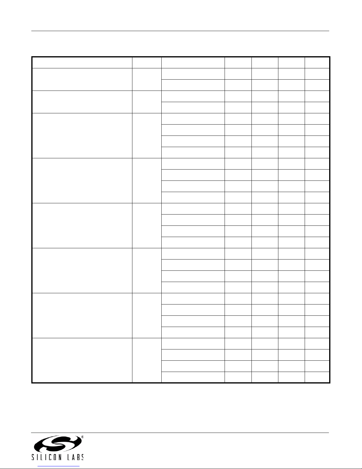
Table 3.16. Comparator
Parameter Symbol Conditions Min Typ Max Units
SiM3U1xx
Response Time, CMPMD = 00
(Highest Speed)
Response Time, CMPMD = 11
(Lowest Power)
Positive Hysterisis
Mode 0 (CPMD = 00)
Negative Hysterisis
Mode 0 (CPMD = 00)
Positive Hysterisis
Mode 1 (CPMD = 01)
t
RESP0
t
RESP3
HYS
HYS
HYS
CP+
CP-
CP+
+100 mV Differential — 100 — ns
–100 mV Differential — 150 — ns
+100 mV Differential — 1.4 — µs
–100 mV Differential — 3.5 — µs
CMPHYP = 00 — 0.37 — mV
CMPHYP = 01 — 7.9 — mV
CMPHYP = 10 — 16.7 — mV
CMPHYP = 11 — 32.8 — mV
CMPHYN = 00 — 0.37 — mV
CMPHYN = 01 — –7.9 — mV
CMPHYN = 10 — –16.1 — mV
CMPHYN = 11 — –32.7 — mV
CMPHYP = 00 — 0.47 — mV
CMPHYP = 01 — 5.85 — mV
CMPHYP = 10 — 12 — mV
CMPHYP = 11 — 24.4 — mV
Negative Hysterisis
Mode 1 (CPMD = 01)
Positive Hysterisis
Mode 2 (CPMD = 10)
Negative Hysterisis
Mode 2 (CPMD = 10)
HYS
HYS
HYS
CP-
CP+
CP-
CMPHYN = 00 — 0.47 — mV
CMPHYN = 01 — –6.0 — mV
CMPHYN = 10 — –12.1 — mV
CMPHYN = 11 — –24.6 — mV
CMPHYP = 00 — 0.66 — mV
CMPHYP = 01 — 4.55 — mV
CMPHYP = 10 — 9.3 — mV
CMPHYP = 11 — 19 — mV
CMPHYN = 00 — 0.6 — mV
CMPHYN = 01 — –4.5 — mV
CMPHYN = 10 — –9.5 — mV
CMPHYN = 11 — –19 — mV
Preliminary Rev. 0.8 27
SiM3U1xx
Table 3.16. Comparator (Continued)
Parameter Symbol Conditions Min Typ Max Units
Positive Hysterisis
HYS
Mode 3 (CPMD = 11)
Negative Hysterisis
HYS
Mode 3 (CPMD = 11)
Input Range (CP+ or CP–) V
Input Pin Capacitance C
IN
CP
Common-Mode Rejection Ratio CMRR
Power Supply Rejection Ratio PSRR
Input Offset Voltage V
Input Offset Tempco TC
Reference DAC Resolution N
OFF
OFF
Bits
CP+
CP-
CP
CP
CMPHYP = 00 — 1.37 — mV
CMPHYP = 01 — 3.8 — mV
CMPHYP = 10 — 7.8 — mV
CMPHYP = 11 — 15.6 — mV
CMPHYN = 00 — 1.37 — mV
CMPHYN = 01 — –3.9 — mV
CMPHYN = 10 — –7.9 — mV
CMPHYN = 11 — –16 — mV
-0.25 — VDD+0.2
V
5
PB2 Pins — 7.5 — pF
PB3 Pins — 10.5 — pF
— 75 — dB
— 72 — dB
TA = 25 °C -5 0 5 mV
— 3.5 — µV/°C
6 bits
28 Preliminary Rev. 0.8
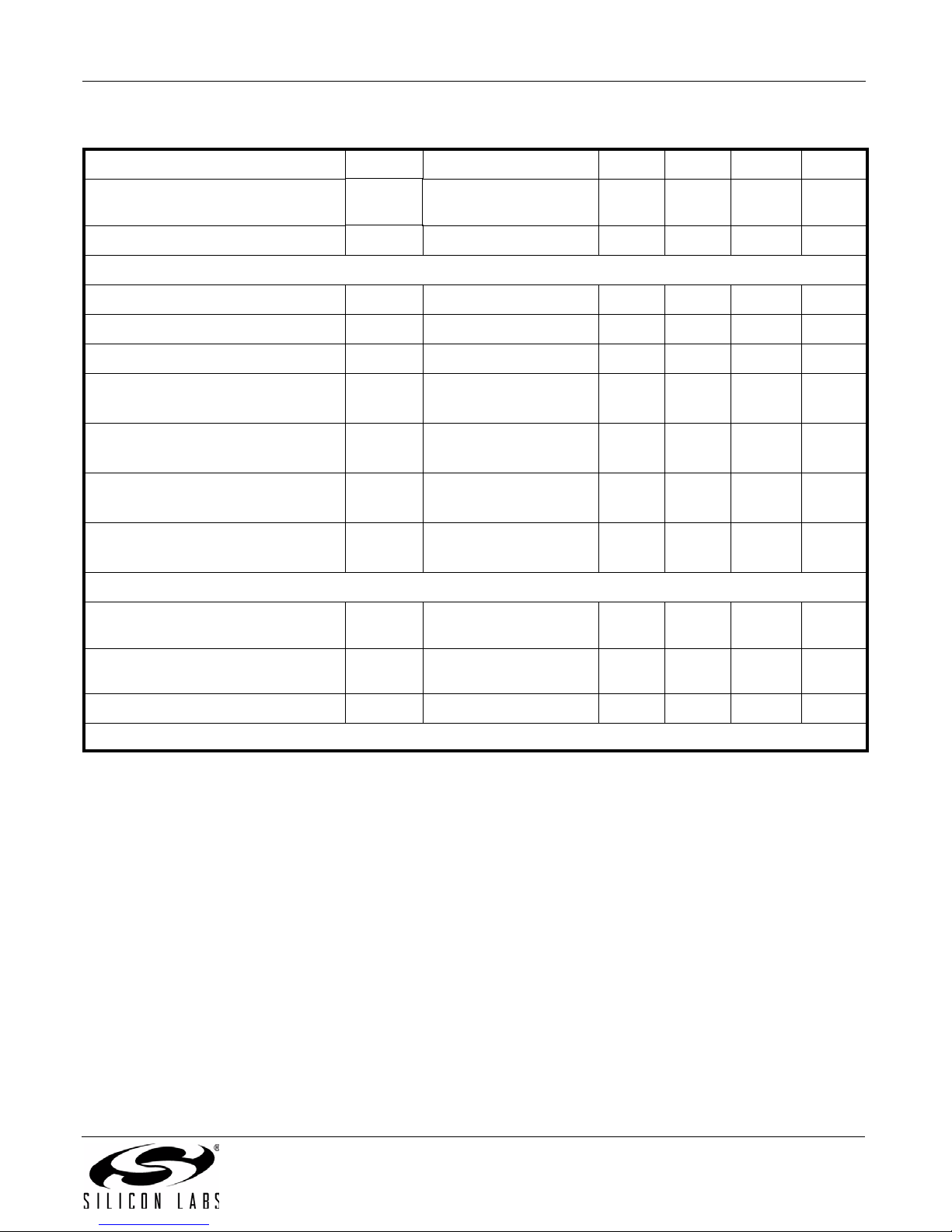
Table 3.17. USB Transciever
Parameter Symbol Conditions Min Typ Max Units
SiM3U1xx
Valid Supply Range
V
DD
(for USB Compliance)
V
VBUS Pull-Down Leakage Current I
VBUSL
= 5 V, VIO = 3.3 V
BUS
Transmitter
Output High Voltage V
Output Low Voltage V
Output Crossover Point V
Output Impedance Z
OH
OL
CRS
DRV
Driving High
Driving Low
Pull-up Resistance R
PU
Full Speed (D+ Pull-up)
Low Speed (D– Pull-up)
Output Rise Time t
R
Low Speed
Full Speed
Output Fall Time t
F
Low Speed
Full Speed
Receiver
Differential Input
V
DI
| (D+) – (D–) | 0.2 — — V
Sensitivity
Differential Input Common Mode
V
CM
Range
Input Leakage Current I
Note: Refer to the USB Specification for timing diagrams and symbol definitions
L
Pullups Disabled — <1.0 — µA
3.0 — 3.6 V
— 10 — µA
2.8 — — V
— — 0.8 V
1.3 — 2.0 V
—
—
38
38
—
—
1.425 1.5 1.575 k
75
4
75
4
—
—
—
—
300
20
300
20
ns
ns
0.8 — 2.5 V
Preliminary Rev. 0.8 29
 Loading...