

Page 1

SiLINKPS-EVB USER’S GUIDE
High
Voltage
Battery
Supply
Low
Voltage
VDD
Supply
Jumper
Selection
JP2, JP3,
JP4
JP6 VDD on/off
JP5 3.3 V/5 V Selector
VDC in
VBRNG
VBHI
VBLO
VDD
AN74
1. Introduction
The SiLinkPS-EVB is a system power supply board that
provides all the necessary supply voltages for a variety
of Silicon Laboratories’ ProSLIC and silicon DAA
evaluation boards. When used with an appropriate ac/
dc wall adapter, the SiLinkPS-EVB can provide up to
25 W of total output power. Table 1 lists some typical
voltages and currents at the power supply outputs.
Table 1. Power Supply Specifications
Input/Output Voltage Current Power
V
IN
VBRNG –96 V 100 mA 9.6 W
VBHI –52 V or
VBLO –26 V 200 mA 5.2 W
V
DD
Any combination of outputs is possible as long as the
simultaneous total power from all outputs does not
exceed the maximum rated 25 W and can be sufficiently
supported by the input power from the V
The SiLinkPS-EVB is designed with the same footprint
as all ProSLIC evaluation board daughter cards
9–15 V 2.5 A 22–37 W
100 mA 5.2 W or
–78 V
7.8 W
3.3 V/5 V 1 A 3.3 W/5 W
.
IN
allowing it to be used in conjunction with multiple
ProSLIC daughter cards to create a modular evaluation
platform.
The SiLinkPS-EVB circuit is based on two power supply
controllers from Linear Technology that provide high
efficiency and low bill-of-materials cost. Both circuits
can be synchronized to the same switching frequency to
reduce power supply switching noise. The outputs can
be configured to support both internal and external
ringing architectures by setting the provided jumpers to
set the desired output voltages. Further modifications
are possible to realize specific output voltage and
current requirements provided the total output power
does not exceed the rated maximum. Schematic
capture and layout gerber files are available for
integration into specific applications. Figure 1 illustrates
a simplified block diagram of the SiLinkPS-EVB supply
board.
2. Operating Instructions
The SiLinkPS-EVB board should always be connected
to the ProSLIC evaluation board platform prior to turning
on the power supply. Plugging any ProSLIC board into a
live high-voltage supply can permanently damage the
ProSLIC ICs. The user should exercise caution when
touching any part of the SiLinkPS-EVB because
dangerous high voltages are present and can cause
injury.
Figure 1. SiLinkPS-EVB Power Supply Simplified Block Diagram
Rev. 0.2 8/03 Copyright © 2003 by Silicon Laboratories AN74-DS02
Page 2

AN74
FREQUENCY (kHz)
100
R
T
(kΩ)
300
1000
10
100
200 1000
900
800700600
500
400
0
2.1. High-Voltage Battery Supply
The schematic for this power circuit is illustrated in
Figure 3 on page 4. The LTC3704 dc-dc controller IC is
used to drive an external MOSFET and a multi-tap
transformer to create four equal high-voltage negative
outputs, VNEG (See Table 2), from the dc input supply.
Only one output is regulated via close-loop feedback.
The other three outputs are cross-regulated to the first
output via the transformer ratio. The LTC3704’s
negative feedback input eliminates inverting circuitry
when creating negative outputs from a positive input.
The six-winding 1:1 ratio transformer is configured in a
manner that minimizes the need for multiple highvoltage output filter capacitors.
2.2. VNEG Voltage Adjustment
The transformer, T1, has four secondary windings, each
producing an equal negative voltage, VNEG. These four
windings are connected in series through the diode
rectifying circuits to produce four negative voltage
potentials with voltage levels equal to multiples from 1
to 4 of the VNEG magnitude. Any adjustment made to
the VNEG has a direct effect on the voltage levels on all
negative outputs.
Resistor R23 can be modified to realize custom output
voltages as defined in the following equation.
VNEG = (1.23 x R23/R22) + 1.23
The SiLinkPS-EVB is shipped with R23 = 33.2 k and
R22 = 1.65 k for VNEG equal to 26 V.
The VBLO is normally used for off-hook state and its
voltage level can be programmed by the setting on the
JP7 jumper. The voltage on the VBHI and VBRNG
outputs can be programmed by moving the jumper
settings on JP2, JP3, and JP4. Table 2 provides several
popular configurations and the required jumper settings.
2.3. Frequency Adjustment
The LTC3704 can be configured to run at switching
frequencies from 50 kHz to 1 MHz allowing flexibility to
choose the optimal efficiency/cost point for each
specific application. Resistor R18 programs the
switching frequency according to the characteristic
curve shown in Figure 2.
Figure 2. Timing Resistor R18 Value
Table 2. Popular Application Configurations and Jumper Settings
Dual ProSLIC
Part Number
Si3211/Si3212
Si3220/Si3232
Si3225 N/A (external) — –52 V
PK-PK Ringing
Amplitude
75 V — –78 V
90 V –104 V
VBRNG VBHI VBLO JP2 JP3 JP4 JP7
4xVNEG
–26 V
3xVNEG
VNEG
—–26V
VNEG
–26 V
2xVNEG
Rev. 0.2 2
VNEG
2–3 2–3 1–2 2–3
1–2 — — 2–3
2–3 — 2–3 2–3
Page 3

AN74
2.4. Low Voltage VDD Supply
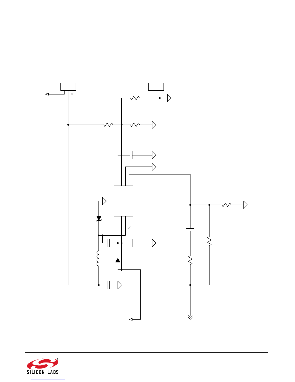
The low-voltage supply provides a switchable 3.3 V or
5 V output with a 1 A maximum load current. The
schematic for this power supply circuit is illustrated in
Figure 4 on page 5. The LT1375 IC integrated 1.5 A
bipolar switching transistor and current-sensing circuitry
eliminate external power transistors and sense resistors
and provide a high-efficiency V
footprint. The switching frequency is internally fixed at
500 kHz and can be synchronized to higher frequencies
up to 1 MHz when a higher frequency signal (above
550 kHz) is provided on the SYNC pin. Table 3 provides
the jumper settings for selecting a 3.3 V or 5 V output as
well as for disconnecting the V
supply in a small
DD
supply altogether.
DD
Table 3. VDD Supply Jumper Settings
Function JP5 JP6 Comments
V
output
DD
enable
3.3 V/5 V
configuration
— 1–2 VDD connected
— 2–3 V
1–2 — 5 V selected
2–3 — 3.3 V selected
disconnected
DD
2.5. Frequency Synchronization
The LTC3704 is wired as a clock master device to
provide its switching frequency to the SYNC pin on the
LT1375 IC. To synchronize the frequency between the
two power circuits, R18 needs to be adjusted to set the
LTC3704 switching frequency at or above 550 kHz. The
LT1375 IC operates at its internal fixed 500 kHz and is
only synchronized with the LTC3704 frequency when it
senses the frequency on the SYNC pin going above
550 kHz. The SiLinkPS-EVB power circuits are
designed to operate safely with switching frequency on
the LTC3704 ranging from 200 kHz to 1 MHz.
2.6. Initialization Steps
1. Configure all jumpers according to the application
requirements.
2. (Optional) Plug in the input power source and
measure all outputs to verify correct settings.
3. Unplug input power source.
4. Assemble all ProSLIC daughter cards.
5. Plug in the input power source.
2.7. Cost-Optimized Design
The negative high-voltage circuit can be reduced for
cost optimization. The four equal VNEG outputs in
series arrangement provide some discrete voltage
adjustments to the outputs but require additional
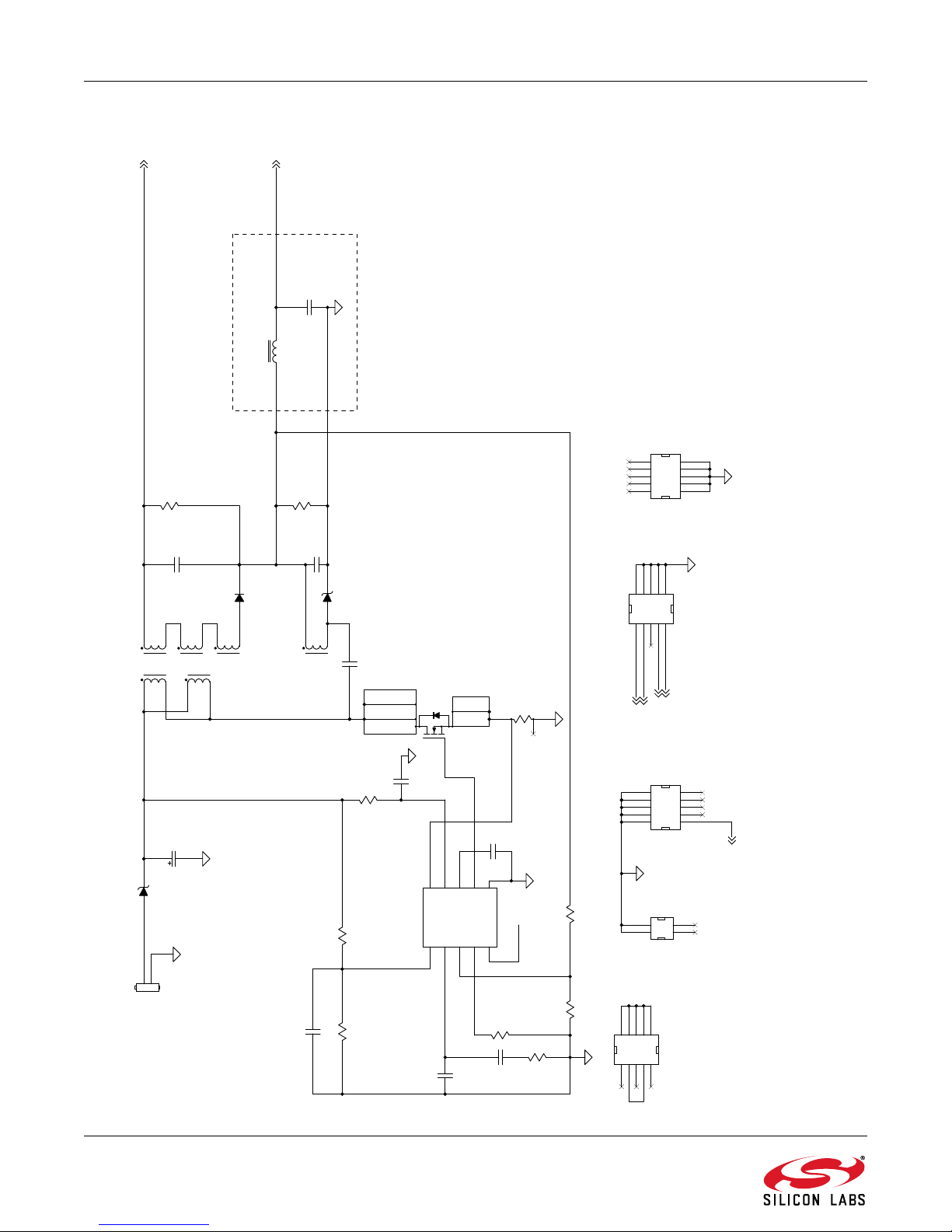
rectifying diode circuits and increase cost. Figure 6 on
page 8 illustrates a lost-optimized design with two
negative outputs. The first secondary winding produces
a negative voltage according to the VNEG equation
described in the previous section to produce the VBLO
voltage. The other three secondary windings are
connected in series to produce a negative voltage with
an amplitude of 3 x VNEG. This output is connected in
series with the VBLO output to generate VBHI output
with a voltage level of 4 x VNEG.
The use of the simplified secondary rectifying circuit,
smaller transformer, and switching MOSFET lower the
component costs and also reduce the maximum output
power of the negative high-voltage circuit to 13 W.
Rev. 0.2 3
Page 4

AN74
IntVcc
IntVcc
-78Vdc
-104Vdc
-25Vdc
-96V
DC_Input
-52V
-78V
-78V
-52V
VBRNG
VBHI
VBLO
DC_Input_Diode
VDD
DC_Input_Diode
VBLO
VBHI
VBRNG
Gate
-52Vdc
VBHI JP3 JP4
-52V X 2-3
-78V 2-3 1-2
-96V 1-2 1-2
VBRNG JP2
-96V 1-2
n/c 2-3
Post-regulator
Turn-on at 9.9V
Turn-off at 9.1V
(Farside)
VBLO JP7
-25V 2-3
-50V 2-1
C9
10uF, 25V
D8
B1100B
JS3
CONN SOCKET 5x2
1
1
2
2
3
3
4
4
5
5
6
6
7
7
8
8
9
9
10
10
C5
10uF, 25V
R8
4.7k
JS1
CONN SOCKET 5x2
112
2
334
4
556
6
778
8
9910
10
R6
10k
R4
10k
R7
100k
C24
330uF 35V
L2
10uH
J1
113
3
C20
100pF
C25
4.7uF, 50V
U2
LTC3704EMS
Run1NFB3Ith
2
Gnd
6
Sense
10
Gate
7
IntVcc
8
Vin
9
Freq4Mode/Sync
5
Q2
IRL540NS
1
2
3
C21
4.7uF, 10V
C22
.001uF
C19
4.7uF, 50V
R21
82k
D5
B1100B
R9
10k
C8
1uF, 25V
R23
33.2k, 1%
R15
10k
R22
1.65k, 1%
R20
.02, 1%
C11
1uF, 25V
JP3
123
JP7
123
D3
CMR3-02
JP4
123
C15
1uF, 25V
T1D
4
9
R17
4.7
T1C
3
10
C18
0.1uF
T1F
6
7
JS2
CONN SOCKET 2x2/SM
1
1
3
3
2
2
4
4
C14
.001uF
T1E
5
8
T1B
2
11
D12
B1100B
C17
10uF, 25V
C13
1uF, 100V
C7
1uF, 100V
JS4
CONN SOCKET 5x2
1
1
2
2
3
3
4
4
5
5
6
6
7
7
8
8
9
9
10
10
JP1
CONN HEADER 2x2/SM
112
2
334
4
R14
82k
R19
47
R13
13k
C23
.001uF
C12
10uF, 25V
D11
B1100B
C10
1uF, 100V
Q1
FZT953CT
JS5
CONN SOCKET 5x2
112
2
334
4
556
6
778
8
9910
10
R11
10k
R25
0
D9
47V
JP2
123
T1A
VP5
1
12
R18
31.6k, 1%
D10
47V
4 Rev. 0.2
Figure 3. High-Voltage Negative Battery Supply
Page 5
VDD
DC_Input_Diode
Gate
5V 1-2
3.3V 2-3
5V or 3.3V
1A Max
VDD on
VDD off
VDD
C3
1uF, 25V
R26
10k
C26
100pF
C4
4.7nF
D2
1N4148
JP5
123
C2
0.1uF
C1
22uF, 6.3V
D1
B1100B
JP6
123
U1
LT1375CS8
BOOST1Vin2Vsw3SHDN
4
SYNC
5
GND
6
FB
7
Vc
8
R1
11.5k, 1%
R2
31.6k, 1%
R3
16.2k, 1%
R28
10k
L1
15uH, 1.8A
R27
10k
AN74
Supply
DD
Figure 4. Low-Voltage V
Rev. 0.2 5
Page 6
AN74
6 Rev. 0.2
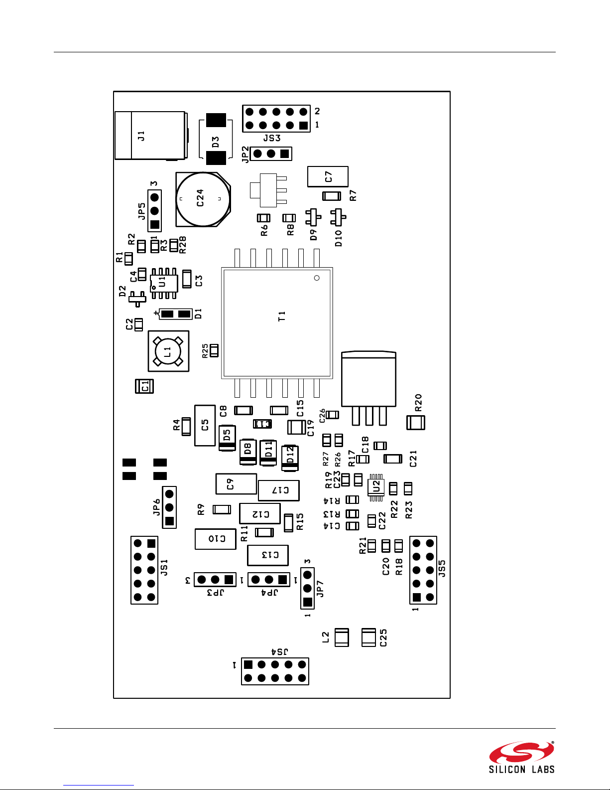
Figure 5. PS Board Silkscreen
Page 7

3. Si Link PS–EVB Bill of Materials
Re fere nce De scription Pa rt Num be r Ma nufa cture r
C1 22uF, 6.3V
C2 0.1uF, 10V
C3,C8,C11,C15 1uF, 25V
C4 4.7nF, 10V
C5,C9,C12,C17 10uF, 25V TMK432BJ106KM Taiyo Yuden
C7,C10,C13 1uF, 100V 18121C105KAT9A United Chemi-con
C22,C14 .001uF, 25V 08055C102KAT AVX
C18 0.1uF, 35V 08053C104KAT AV X
C16, C19 4.7uF, 50V C5750X7R1H475K TDK
C20,C26 100pF, 25V 08055A101KAT AVX
C21 4.7uF, 10V LMK316BJ475 Taiyo Yuden
C23 .001uF, 25V
C24 330uF, 35V
D2 1N4148 Diodes, Inc.
D3 ES3A/B ES3A/B Diodes, Inc.
D1,D5,D8,D11,D12 B1100B B160B Diodes, Inc.
D9,D10 47V Zener
JP1 CONN HEADER 2x2/SM TSM-102-02-T-DV Samtec
JP2,JP3,JP4,JP5,JP6,JP7 HEADER 3X1 2303-6111TN 3M
JS1,JS3,JS4,JS5 CONN SOCKET 5x2 SSQ-1-05-24-F-D Samtec
JS2 CONN SOCKET 2x2/SM SSM-102-L-DV-TR Samtec
J1 CONN PW R 2-P A DC-002-1 Adam Tech
L1 15uH, 1.8A UP1B-150 Coiltronics
L2 10uH CTX32CT-100 Coiltronics
Q1 FZT953CT FZT953CT Zetex
Q2 IRL540NS IRL540NS Int. Rectifier
R1 11.5k, 1%
R2 31.6k
R3 16.2k
R4,R9,R11,R15,R26,R27,R28 10k
R6 10k
R7 100k
R8 4.7k
R13 13k
R21,R14 82k
R17 4.7
R18 120k
R19 47
R20 15m
LRC1206-R015K IRC
R22 1.65k
R23 33.2k
R25 0
T1 VP5 VPH5-0155 Coiltronics
U1 LT1375CS8 LT1375CS8 LTC
U2 LTC3704EMS LTC3704CMS LTC
Rev. 0.2 7
AN74
Page 8
AN74
IntVcc
IntVcc
-24Vdc
DC_Input -96Vdc
VBHI
VBLO
DC_Input_Diode
VDD
VBRNG
VBLO
VBHI
Turn-on at 9V
Turn-off at 8.2V
T1: 10uH
L2 and C16 optional for lower output noi se.
In Proto:
R23 = 20.5k
R22 = 1.1k
C5 = 2 x 1uF / 100V in parallel
R4 = 3 x 10k in series
Q2 is upside-down
36k = 500kHz
20k = 1MHz
10~15Vdc
Input
JS4
CONN SOCKET 5x2
1
1
2
2
3
3
4
4
5
5
6
6
7
7
8
8
9
9
10
10
C5
2.2uF, 100V
C16
10uF, 25V
JS3
CONN SOCKET 5x2
112
2
334
4
556
6
778
8
9910
10
R4
30k
C24
330uF 35V
L2
10uH
C20
680pF
JP1
113
3
U2
LTC3704EMS
Run1NFB3Ith
2
Gnd
6
Sense
10
Gate
7
IntVcc
8
Vin
9
Freq4Mode/Sync
5
C22
.01uF
C21
4.7uF, 10V
R21
82k
C19
4.7uF, 50V
R20
.015, 5%
JS1
CONN SOCKET 5x2
1
1
2
2
3
3
4
4
5
5
6
6
7
7
8
8
9
9
10
10
R15
10k
R23
34.8k, 1%
R22
1.87k, 1%
Q2
Si4480DY
4
5
1
6
2 3
7 8
D4
ES1D
D3
B340
R18
36k
T1D
4
9
R17
4.7
T1C
3
10
C18
0.1uF
T1F
6
7
T1E
5
8
C14
.001uF
T1B
2
11
D12
B1100B
C17
10uF, 25V
JS2
CONN SOCKET 2x2
1
1
3
3
2
2
4
4
R14
82k
R13
16k
JS5
CONN SOCKET 5x2
112
2
334
4
556
6
778
8
9910
10
T1A
VP5
1
12
8 Rev. 0.2
Figure 6. Cost-Optimized Dual Output Battery Supply
Page 9
AN74
C18
08053C104KAT AVX
C5
C5750X7R2A225M TDK
C22, C14 1 nF, 25 V, X7R
C16*, C17
TMK432BJ106KM Taiyo Yuden
C19
UMK325F475KH Taiyo Yuden
C20
08055A101KAT AVX
C21
LMK316BJ475 Taiyo Yuden
C24
35CV330AX Sanyo
D3 40 V, 3 A B340 Diodes, Inc.
D4 200 V, 1 A ES1D Diodes, Inc.
D12 100 V, 1 A Shottky B1100B Diodes, Inc.
L2*
CTX32CT-470 Coiltronics
Q2 80 V Si4480DY Vishay
R4
R13
R21, R14
R15
R17
R18
R20
R22
R23
T1
SP36-0100-10 Transpower
U2 Switching Regulator LTC3704EMS LTC
Note: * Optional components used to reduce output noise if necessary.
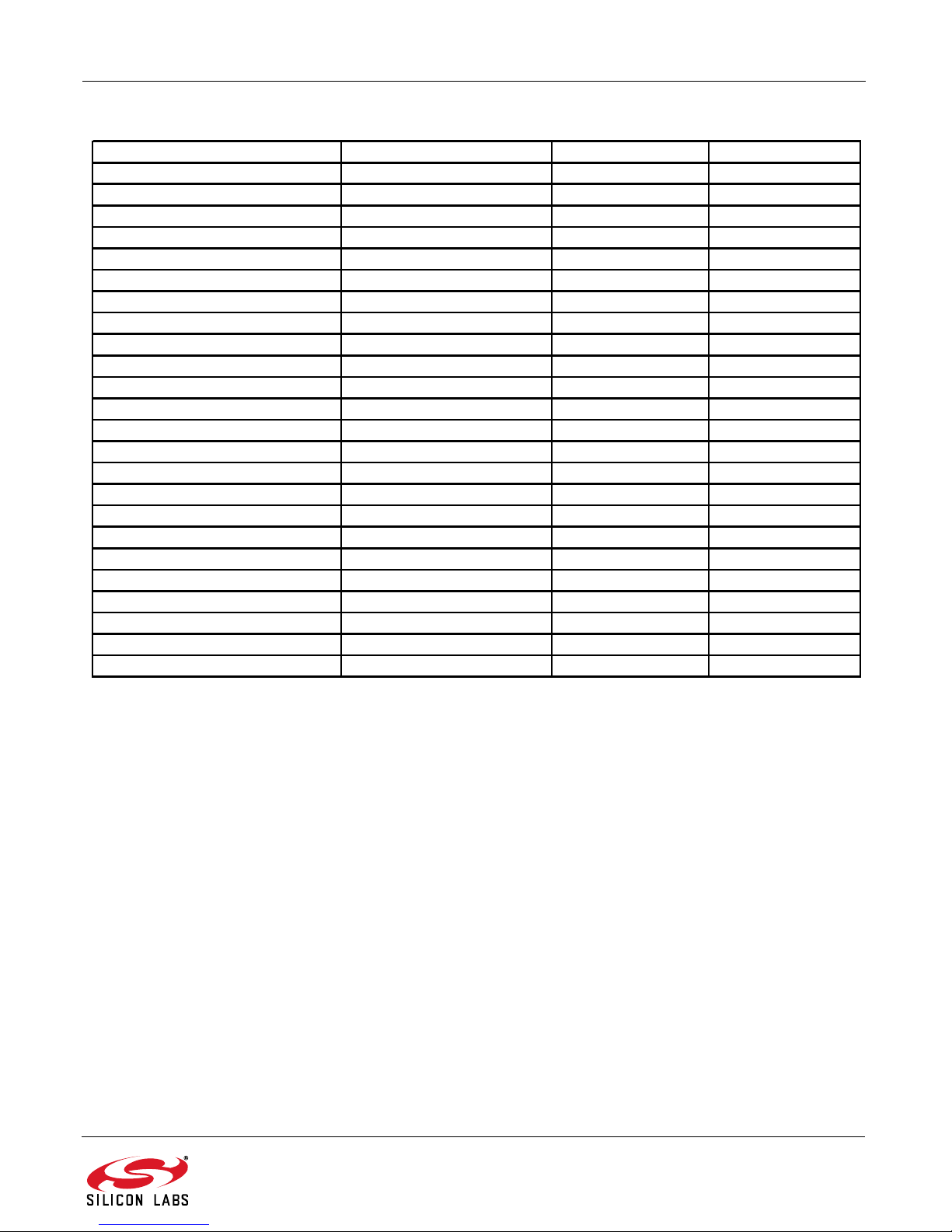
4. Cost-Optimized Dual Output Battery Supply Bill of Materials
Reference Description Part Number Manufacturer
0.1 F, 25 V, X7R
2.2 F, 100 V, X7R
10 F, 25 V, X5R
4.7 F, 50 V, X7R
100 pF, 50 V, NP0
4.7 F, 10 V, X5R
330 F, 35 V
10 H, 300 mA
30 k, 5%, 0.25 W
16 k, 5%, 0.1 W
82 k, 5%, 0.1 W
10 k, 5%, 0.1 W
4.7 , 5%, 0.1 W
36 k, 5%, 0.1 W
15 m, 5%, 0.25 W
1.87 k, 1%, 0.1 W
34.8 k, 1%, 0.1 W
10 H
Rev. 0.2 9
Page 10

AN74
DOCUMENT CHANGE LIST
Revision 0.1 to Revision 0.2
New power supply schematics
Updated Figures 3, 4, and 5.
Updated document to support two levels of VBATL
voltage.
10 Rev. 0.2
Page 11

NOTES:
AN74
Rev. 0.2 11
Page 12
Smart.
Connected.
Energy-Friendly
Products
www.silabs.com/products
Disclaimer
Silicon Laboratories intends to provide customers with the latest, accurate, and in-depth documentation of all peripherals and modules available for system and software implementers
using or intending to use the Silicon Laboratories products. Characterization data, available modules and peripherals, memory sizes and memory addresses refer to each specific
device, and "Typical" parameters provided can and do vary in different applications. Application examples described herein are for illustrative purposes only. Silicon Laboratories
reserves the right to make changes without further notice and limitation to product information, specifications, and descriptions herein, and does not give warranties as to the accuracy
or completeness of the included information. Silicon Laboratories shall have no liability for the consequences of use of the information supplied herein. This document does not imply
or express copyright licenses granted hereunder to design or fabricate any integrated circuits. The products must not be used within any Life Support System without the specific
written consent of Silicon Laboratories. A "Life Support System" is any product or system intended to support or sustain life and/or health, which, if it fails, can be reasonably expected
to result in significant personal injury or death. Silicon Laboratories products are generally not intended for military applications. Silicon Laboratories products shall under no
circumstances be used in weapons of mass destruction including (but not limited to) nuclear, biological or chemical weapons, or missiles capable of delivering such weapons.
Trademark Information
Silicon Laboratories Inc., Silicon Laboratories, Silicon Labs, SiLabs and the Silicon Labs logo, CMEMS®, EFM, EFM32, EFR, Energy Micro, Energy Micro logo and combinations
thereof, "the world’s most energy friendly microcontrollers", Ember®, EZLink®, EZMac®, EZRadio®, EZRadioPRO®, DSPLL®, ISOmodem ®, Precision32®, ProSLIC®, SiPHY®,
USBXpress® and others are trademarks or registered trademarks of Silicon Laboratories Inc. ARM, CORTEX, Cortex-M3 and THUMB are trademarks or registered trademarks of
ARM Holdings. Keil is a registered trademark of ARM Limited. All other products or brand names mentioned herein are trademarks of their respective holders.
Silicon Laboratories Inc.
400 West Cesar Chavez
Austin, TX 78701
USA
Quality
www.silabs.com/quality
Support and Community
community.silabs.com
http://www.silabs.com
 Loading...