


Si84xxISO-EVB UG
Si84XXISO EVALUATION BOARD USER ’S GUIDE
1. Introduction
The Si84xxISO evaluation board allows designers to evaluate Silicon Lab's family of CMOS ultra-low-power
isolators. These isolators are CMOS devices employing RF coupler technology to transmit digital information
across an isolation barrier. Very high speed operation at low power levels is achieved. These products are based
on Silicon Laboratories’ proprietary RF isolation technology and offer shorter propagation delays, lower power
consumption, improved noise immunity, smaller inst alled size, and mor e st able oper ation with tempe rature and age
versus opto couplers. The Si841x/2x/3x/4x/5x/6x include up to six unidirectional isolated channels, permitting data
transmission up to 150 Mbps. The Si840x isolator series cons ists of sing le- package g alv an ic is ola tio n solutions for
2
C, SMBus, and PMBus serial port applications. For more information, refer to the respective family data sheets.
I
A summary of the benefits provided by the Silicon Laboratories Si84xx CMOS Digital Isolator family includes:
Robust Noise Tolerance:
5.0 kV, 2.5 kV, and 1.0 kV Isolation Ratings
Up to 50 V/m Electric-field immunity
> 1000 A/m Magnetic-field immunity
25 kV/µs CMTI
FCC Class B Compliant
Class-leading ESD Performance:
4 kV HBM, 2 kV CDM, 400 V MM
Ultra Low Power Operation:
< 1.4 mA/Channel @ 1 Mbps
200 µA stan dby mode
High Speed Operation:
DC–150 Mbps from –40 to 125 °C
< 250 ps (peak) Jitter
Precise Timing:
1.5 ns pulse width distortion
0.5 ns channel-channel matching
2 ns pulse width skew
2
I
C Compatible Isolators:
Bidirectional isolated Serial Data (SDA) and Serial Clock
Data Rates up to 1.7 Mbps
35 mA open drain I/O
Flexible Packaging Options:
NB SOIC-8, WB SOIC-16, NB SOIC-16
RoHS compliant
Rev. 0.3 8/10 Copyright © 2010 by Silicon Laboratories Si84xxISO-EVB UG
Si84xxISO-EVB UG
2. Kit Contents
The Si84xxISO Evaluation Kit contains the following items:
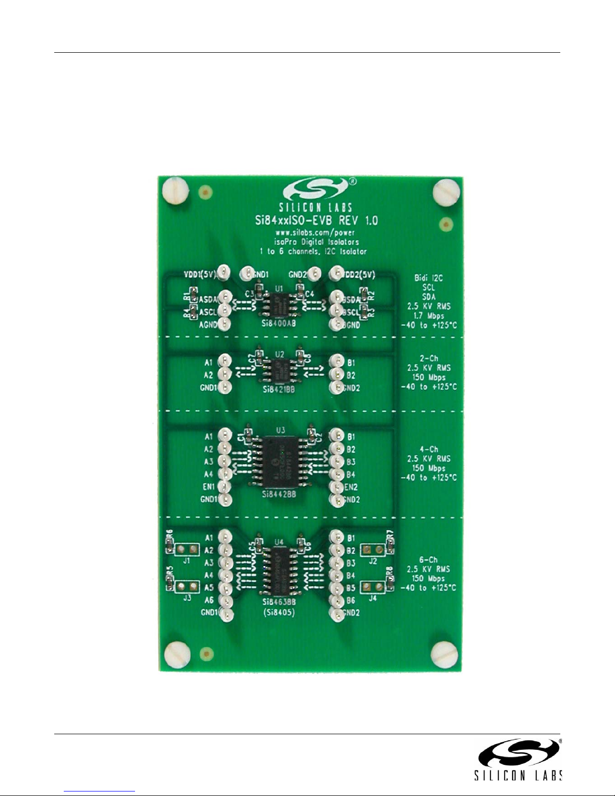
Si84xxISO based evaluation board (Si84xxISO-EVB or Si84xx5kVISO-EVB) shown in Figures 1 and 2.
Si8400, Si8421, Si8442, Si8463, Si8420 (5 kV), and Si8422 (5 kV) CMOS digital isolators installed on the
evaluation board
Figure 1. Si84xxISO Evaluation Board Overview
2 Rev. 0.3
Si84xxISO-EVB UG
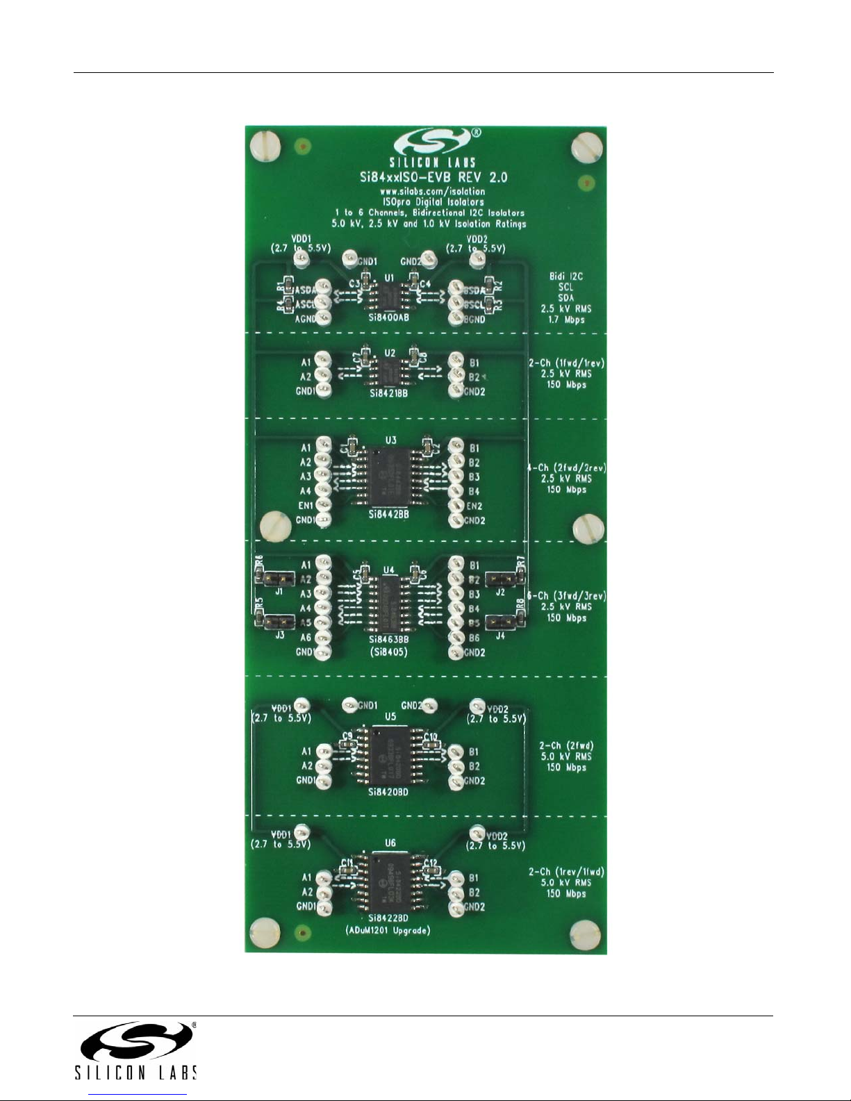
Figure 2. Si84xx5kVISO Evaluation Board Overview
Rev. 0.3 3
Si84xxISO-EVB UG
3. Hardware Overview and Setup
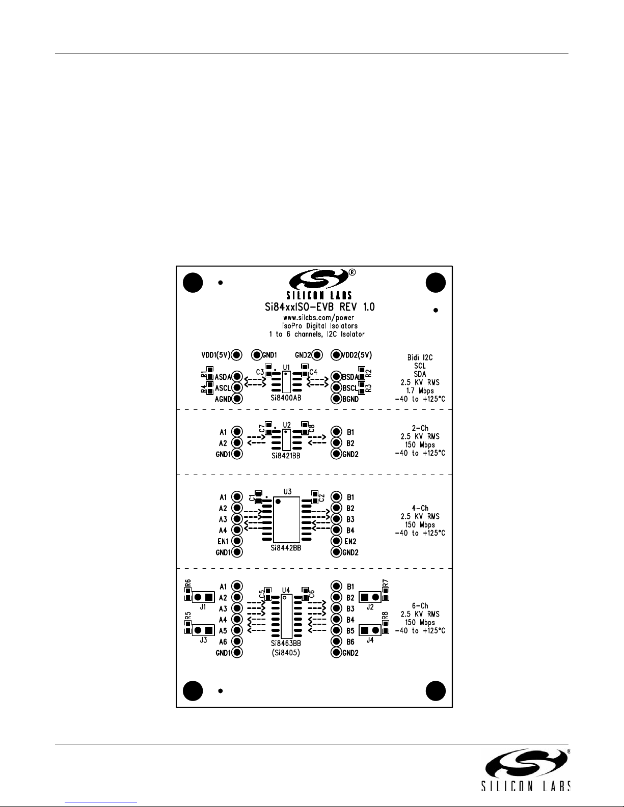
The Si84xxISO evaluation board comes populated with an Si8400 (isolated I2C), Si8421 (2-channel digital isolator,
one forward, one reverse), Si8442 (4-channel digital isolator, two forward, two reverse), and Si8463 (6-channel
digital isolator, three forward, three reverse) installed. The Si84xx5kVISO-EVB adds the Si8420 and Si8422 5 kV
family members. The board is designed to be powered from two separate 5 V supplies (500 mA) that power all the
isolators on the board. Power is applied to the board before evaluating any isolated channel. Power is applied to
the Si84xxISO-EVB by connecting 5 V supplies to the topmost supply terminals (VDD1 and GND1, VDD2 and
GND2). Power is applied to the Si84xx5kVISO-EVB by applying 5 V supplies to the topmost and middle power
terminals (VDD1 and GND1, VDD2 and GND2). The top po wer terminals power the 2.5 kV isolators. The middle
power terminals power the 5 kV isolators. Supplies as low as 2.7 V can be used. If a user wants to evaluate an
isolator other than the ones populated, this can be accomplished by removing the footprint-compatible device
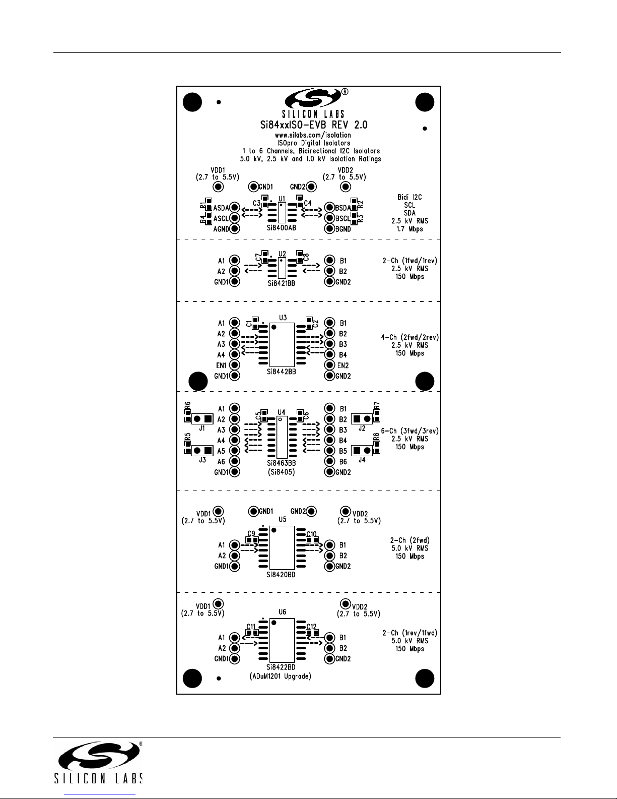
installed on the evaluation board and replacing it with the desired isolator device. Figures 3 and 5 provide
silkscreen overviews of the boards.
Figure 3. Si84xxISO Evaluation Board Silkscreen
4 Rev. 0.3
Si84xxISO-EVB UG
Figure 4. Si84xx5kVISO Evaluation Board Silkscreen
Rev. 0.3 5
Si84xxISO-EVB UG
3.1. Digital Isolator Considerations
The Si84xxISO evaluation board (see Figure 1 on page 2) provides a means to evaluate the Si841x,2x,3x,4x,5x,6x
digital isolator families as well as the Si8400 isolated I
connect a digital input signal (5 Vpeak max, with desired clock frequency up to 150 Mbps) to the desired input
channel. To view the isolated channel’s data tr ansmission , co nnect a scop e probe to the output chan nel of interest.
There are various inputs and outp ut s on e ither side of the bo ard d ependin g on the d evice o ne ch ooses to evaluate,
as indicated by the silk screen. The board can be used to measure propagation delay, pulse-width distortion,
channel-channel matching, pulse-width skew, and various other parameters.
The nominal output impedance of an isolator driver channel is approximately 50 , ±40%, which is a combination
of the values of the on-chip series termination resistor and the channel resistance of the output driver FET. When
driving loads where transmission line effects will be a factor, output pins should be terminated with 50 controlled
impedance PCB traces.
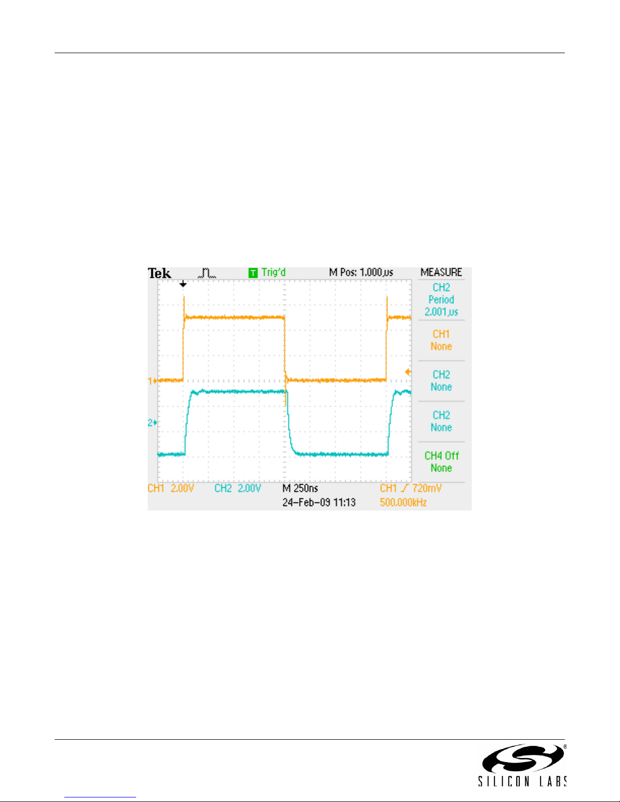
Figure 5 illustrates the Si8421 transmitting a 500 kHz (5 Vpeak) signal through the Si8421. VDD1 and VDD2 were
powered from 5 V. Channel 1 illustrates the input, and Channel 2 illustrates the output.
2
C family. After power has been supplied to the board,
6 Rev. 0.3
Figure 5. 500 kHz (5 V Peak) Signal
 Loading...