

TRIPLE-CHANNEL DIGITAL ISOLATOR
Si8430/31/35
Features
High-speed operation:
DC – 150 Mbps
Low propagation delay:
<10 ns
Wide Operating Supply Voltage:
2.375-5.5V
Low power: I1 + I2 <
12 mA/channel at 100 Mbps
Precise timing:
2 ns pulse width distortion
1 ns channel-channel matching
2 ns pulse width skew
Applications
Isolated switch mode supplies
Isolated ADC, DAC
Safety Regulatory Approvals
UL recognition:2500 V
Minute per UL1577
CSA component acceptance
notice
RMS
for 1
2500 V
Transient Immunity: >25 kV/µs
Tri-state outputs with ENABLE
RMS
isolation
control
DC correct
No start-up initialization required
<10 µs Startup Time
High temperature operation:
125 °C at 100 Mbps
100 °C at 150 Mbps
Wide body SOIC-16 package
Motor control
Power factor correction systems
VDE certification conformity
IEC 60747-5-2
(VDE0884 Part 2)
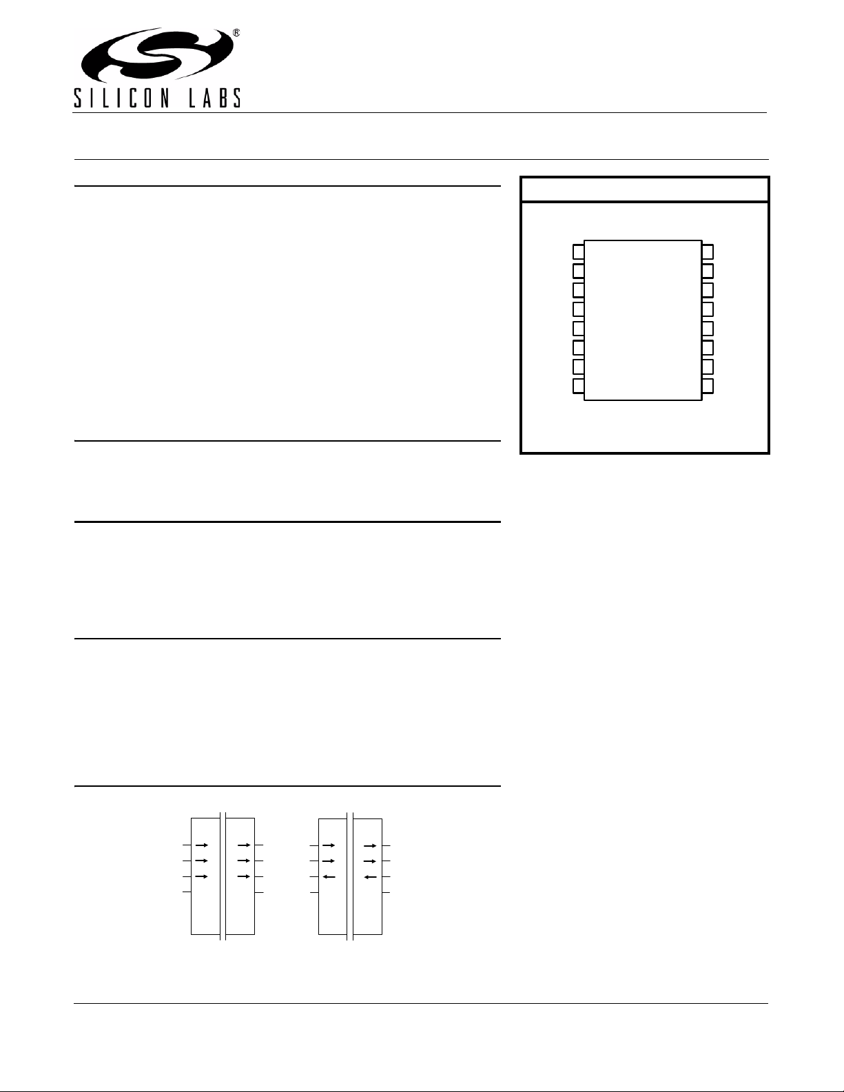
V
DD1
GND1
A1
A2
A3
NC
EN1/NC
GND1
Pin Assignments
Wide Body SOIC
1
2
3
4
5
6
7
8
Top View
16
15
14
13
12
11
10
9
V
DD2
GND2
B1
B2
B3
NC
EN2/NC
GND2
Description
Silicon Lab's family of digital isolators are CMOS devices that employ
an RF coupler to transmit digital information across an isolation
barrier. Very high speed operation at low power levels is achieved.
These parts are available in a 16-pin wide body SOIC package. Three
speed grade options (1, 10, 150 Mbps) are available and achieve
typical propagation delay of less than 10 ns.
Block Diagram
Si8430/35
A1
A2
A3
NC
B1
B2
B3
Rev. 0.31 5/08 Copyright © 2008 by Silicon Laboratories Si8430/31/35
Si8431
A1
A2
A3
EN1EN2/NC EN2
B1
B2
B3

Si8430/31/35
2 Rev. 0.31

Si8430/31/35
TABLE OF CONTENTS
Section Page
1. Electrical Specifications . . . . . . . . . . . . . . . . . . . . . . . . . . . . . . . . . . . . . . . . . . . . . . . . . . . 4
2. Typical Performance Characteristics . . . . . . . . . . . . . . . . . . . . . . . . . . . . . . . . . . . . . . . .17
3. Application Information . . . . . . . . . . . . . . . . . . . . . . . . . . . . . . . . . . . . . . . . . . . . . . . . . . .19
3.1. Theory of Operation . . . . . . . . . . . . . . . . . . . . . . . . . . . . . . . . . . . . . . . . . . . . . . . . .19
3.2. Eye Diagram . . . . . . . . . . . . . . . . . . . . . . . . . . . . . . . . . . . . . . . . . . . . . . . . . . . . . . .19
4. Layout Recommendations . . . . . . . . . . . . . . . . . . . . . . . . . . . . . . . . . . . . . . . . . . . . . . . .20
4.1. Supply Bypass . . . . . . . . . . . . . . . . . . . . . . . . . . . . . . . . . . . . . . . . . . . . . . . . . . . . .20
4.2. Input and Output Characteristics . . . . . . . . . . . . . . . . . . . . . . . . . . . . . . . . . . . . . . . . 21
4.3. Enable (EN1, EN2) Inputs . . . . . . . . . . . . . . . . . . . . . . . . . . . . . . . . . . . . . . . . . . . . .22
4.4. RF Radiated Emissions . . . . . . . . . . . . . . . . . . . . . . . . . . . . . . . . . . . . . . . . . . . . . . . 23
4.5. RF Immunity and Common Mode Transient Immunity . . . . . . . . . . . . . . . . . . . . . . . 24
5. Pin Descriptions . . . . . . . . . . . . . . . . . . . . . . . . . . . . . . . . . . . . . . . . . . . . . . . . . . . . . . . . . 25
6. Ordering Guide . . . . . . . . . . . . . . . . . . . . . . . . . . . . . . . . . . . . . . . . . . . . . . . . . . . . . . . . . . 26
7. Package Outline: Wide Body SOIC . . . . . . . . . . . . . . . . . . . . . . . . . . . . . . . . . . . . . . . . . .27
Document Change List . . . . . . . . . . . . . . . . . . . . . . . . . . . . . . . . . . . . . . . . . . . . . . . . . . . . .28
Contact Information . . . . . . . . . . . . . . . . . . . . . . . . . . . . . . . . . . . . . . . . . . . . . . . . . . . . . . . .30
Rev. 0.31 3
Si8430/31/35
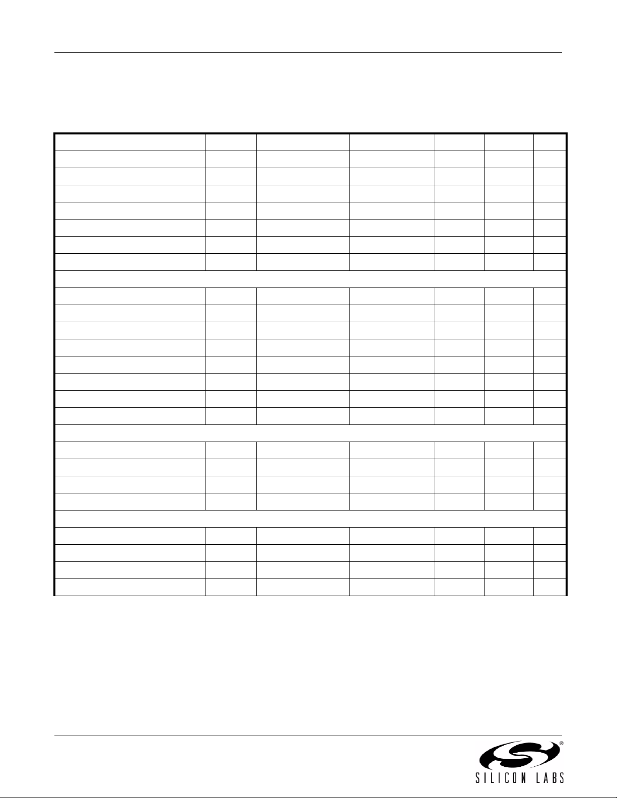
1. Electrical Specifications
Table 1. Electrical Characteristics
(V
= 5 V, V
DD1
Parameter Symbol Test Condition Min Typ Max Unit
= 5 V, TA = –40 to 125 ºC)
DD2
High Level Input Voltage V
Low Level Input Voltage V
High Level Output Voltage V
Low Level Output Voltage V
Input Leakage Current I
Enable Input High Current I
Enable Input Low Current I
DC Supply Current (All inputs 0 V or at Supply)
Si8430/35-A,-B,-C, V
Si8430/35-A,-B,-C, V
Si8430/35-A,-B,-C, V
Si8430/35-A,-B,-C, V
Si8431-A,-B,-C, V
Si8431-A,-B,-C, V
Si8431-A,-B,-C, V
Si8431-A,-B,-C, V
DD1
DD2
DD1
DD2
DD1
DD2
DD1
DD2
10 Mbps Supply Current (All inputs = 5 MHz square wave, CI = 15 pF on all outputs)
Si8430/35-B,-C, V
Si8430/35-B,-C, V
Si8431-B,-C, V
Si8431-B,-C, V
DD1
DD2
DD1
DD2
100 Mbps Supply Current (All inputs = 50 MHz square wave, CI = 15 pF on all outputs)
Si8430-C, V
Si8430-C, V
Si8431-C, V
Si8431-C, V
DD1
DD2
DD1
DD2
IH
IL
OH
OL
L
ENH
ENL
2.0 — — V
——0.8V
loh = –4 mA V
DD1,VDD2
–0.4 4.8 — V
lol = 4 mA — 0.2 0.4 V
——±10µA
V
V
ENx
ENx
= V
= V
IH
IL
—4—µA
—20—µA
All inputs 0 DC — 7 10 mA
All inputs 0 DC — 6 9 mA
All inputs 1 DC — 14 18 mA
All inputs 1 DC — 6 9 mA
All inputs 0 DC — 8 12 mA
All inputs 0 DC — 10 15 mA
All inputs 1 DC — 13 19 mA
All inputs 1 DC — 12 17 mA
—1115mA
—1317mA
—1216mA
—1317mA
—1115mA
—2328mA
—1318mA
—2126mA
4 Rev. 0.31
Si8430/31/35
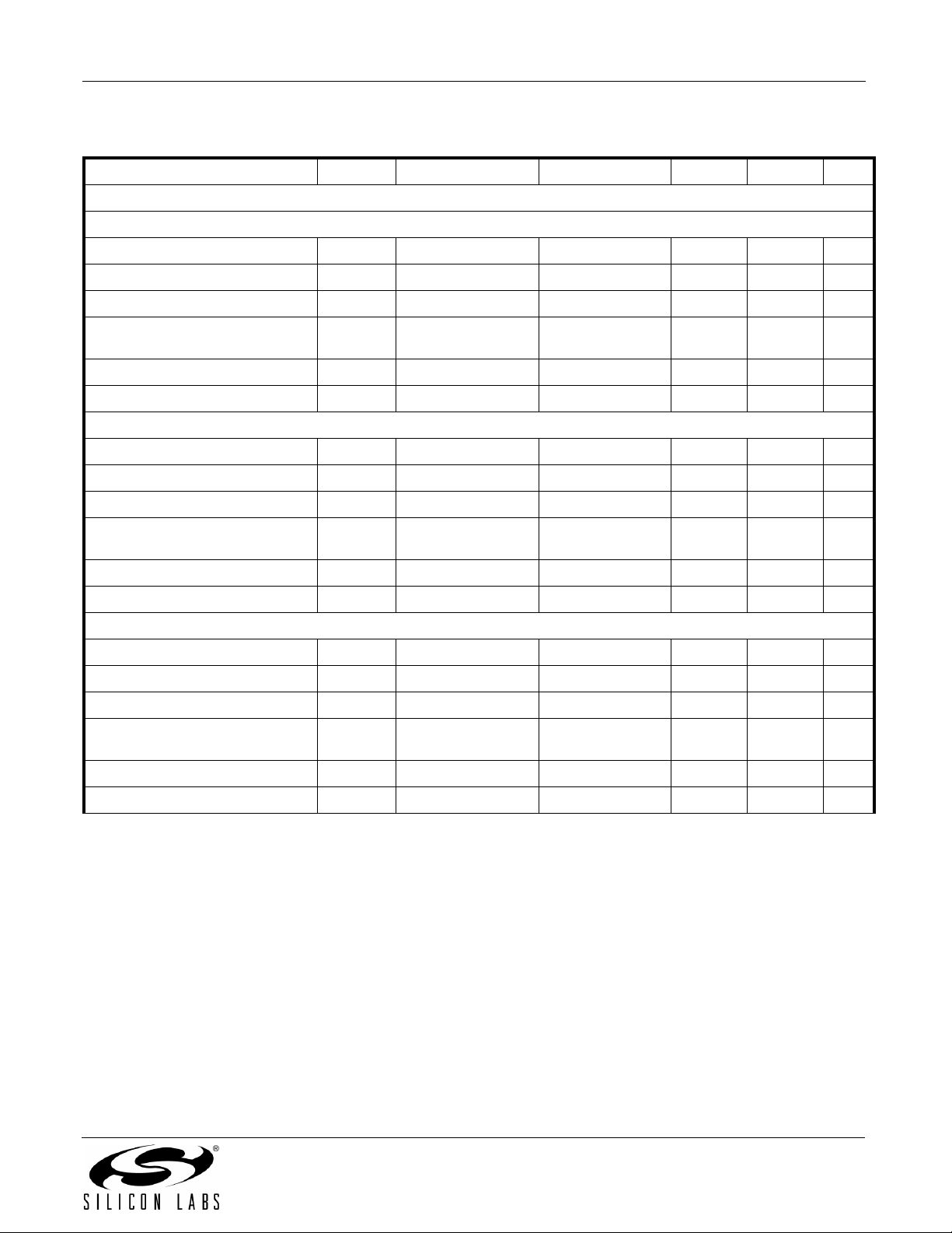
Table 1. Electrical Characteristics (Continued)
(V
= 5 V, V
DD1
Parameter Symbol Test Condition Min Typ Max Unit
Si843x-A
Maximum Data Rate 0 — 1 Mbps
Minimum Pulse Width — — 1000 ns
Propagation Delay t
Pulse Width Distortion
|t
PLH - tPHL
Propagation Delay Skew
Channel-Channel Skew t
Si843x-B
Maximum Data Rate 0 — 10 Mbps
Minimum Pulse Width — — 100 ns
= 5 V, TA = –40 to 125 ºC)
DD2
|
1
Timing Characteristics
PHL
, t
PLH
See Figure 2 — — 75 ns
PWD See Figure 2 — — 30 ns
t
PSK(P-P)
PSK
— — 50 ns
— — 40 ns
Propagation Delay t
Pulse Width Distortion
|t
PLH - tPHL
Propagation Delay Skew
|
1
Channel-Channel Skew t
PHL
, t
PLH
See Figure 2 — — 35 ns
PWD See Figure 2 — — 7.5 ns
t
PSK(P-P)
PSK
— — 25 ns
——5ns
Si843x-C
Maximum Data Rate 0 — 150 Mbps
Minimum Pulse Width — — 6.6 ns
Propagation Delay t
Pulse Width Distortion
|t
PLH - tPHL
Propagation Delay Skew
|
1
Channel-Channel Skew t
PHL
, t
PLH
See Figure 2 4 6.5 9.5 ns
PWD See Figure 2 — — 3 ns
t
PSK(P-P)
PSK
——5.5ns
——3ns
Rev. 0.31 5
Si8430/31/35
Table 1. Electrical Characteristics (Continued)
(V
= 5 V, V
DD1
Parameter Symbol Test Condition Min Typ Max Unit
For All Models
Output Rise Time t
Output Fall Time t
Common Mode Transient
Immunity
Enable to Data Valid t
Enable to Data Tri-State t
Start-up Time
Notes:
1. t
PSK(P-P)
same supply voltages, load, and ambient temperature.
2. Start-up time is the time period from the application of power to valid data at the output.
= 5 V, TA = –40 to 125 ºC)
DD2
r
CL = 15 pF
—2—ns
See Figure 2
f
CL = 15 pF
—2—ns
See Figure 2
CMTI V
en1
en2
2
is the magnitude of the difference in propagation delay times measured between different units operating at the
t
SU
I=VDD
See Figure 1 — 5 — ns
See Figure 1 — 5 — ns
or 0 V 25 30 — kV/µs
—3—µs
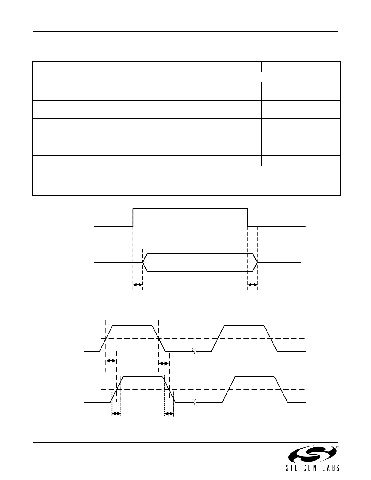
ENABLE
OUTPUTS
Typical
Input
Typical
Output
50%
50%
t
en1
Figure 1. ENABLE Timing Diagram
t
PLH
90%
10%
t
r
90%
10%
t
PHL
t
f
t
en2
Figure 2. Propagation Delay Timing
6 Rev. 0.31
Si8430/31/35
Table 2. Electrical Characteristics
(V
= 3.3 V, V
DD1
Parameter Symbol Test Condition Min Typ Max Unit
= 3.3 V, TA = –40 to 125 ºC)
DD2
High Level Input Voltage V
Low Level Input Voltage V
High Level Output Voltage V
Low Level Output Voltage V
Input Leakage Current I
Enable Input High Current I
Enable Input Low Current I
DC Supply Current (All inputs 0 V or at supply)
Si8430/35-A,-B,-C, V
Si8430/35-A,-B,-C, V
Si8430/35-A,-B,-C, V
Si8430/35-A,-B,-C, V
Si8431-A,-B,-C, V
Si8431-A,-B,-C, V
Si8431-A,-B,-C, V
Si8431-A,-B,-C, V
DD1
DD2
DD1
DD2
DD1
DD2
DD1
DD2
10 Mbps Supply Current (All inputs = 5 MHz square wave, CI = 15 pF on all outputs)
IH
IL
OH
OL
L
ENH
ENL
2.0 — — V
——0.8V
loh = –4 mA V
DD1,VDD2
–0.4 3.1 — V
lol = 4 mA — 0.2 0.4 V
——±10µA
V
V
ENx
ENx
= V
= V
IH
IL
—4—µA
—20—µA
All inputs 0 DC — 7 10 mA
All inputs 0 DC — 6 9 mA
All inputs 1 DC — 13 17 mA
All inputs 1 DC — 5 8 mA
All inputs 0 DC — 7 11 mA
All inputs 0 DC — 10 15 mA
All inputs 1 DC — 12 18 mA
All inputs 1 DC — 11 16 mA
Si8430/35-B,-C, V
Si8430/35-B,-C, V
Si8431-B,-C, V
Si8431-B,-C, V
DD1
DD2
100 Mbps Supply Current (All inputs = 50 MHz square wave, CI = 15 pF on all outputs)
Si8430-C, V
Si8430-C, V
Si8431-C, V
Si8431-C, V
DD1
DD2
DD1
DD2
DD1
DD2
—1014mA
—1116mA
—1015mA
—1318mA
—1115mA
—1620mA
—1218mA
—1925mA
Rev. 0.31 7
Si8430/31/35
Table 2. Electrical Characteristics (Continued)
(V
= 3.3 V, V
DD1
Parameter Symbol Test Condition Min Typ Max Unit
Si843x-A
Maximum Data Rate 0 — 1 Mbps
Minimum Pulse Width — — 1000 ns
= 3.3 V, TA = –40 to 125 ºC)
DD2
Timing Characteristics
Propagation Delay t
Pulse Width Distortion
|t
PLH - tPHL
Propagation Delay Skew
|
1
Channel-Channel Skew t
PHL
, t
PLH
See Figure 2 — — 75 ns
PWD See Figure 2 — — 30 ns
t
PSK(P-P)
PSK
— — 50 ns
— — 40 ns
Si843x-B
Maximum Data Rate 0 — 10 Mbps
Minimum Pulse Width — — 100 ns
Propagation Delay t
Pulse Width Distortion
|t
PLH - tPHL
Propagation Delay Skew
|
1
Channel-Channel Skew t
PHL
, t
PLH
See Figure 2 — — 35 ns
PWD See Figure 2 — — 7.5 ns
t
PSK(P-P)
PSK
— — 25 ns
——5ns
Si843x-C
Maximum Data Rate 0 — 150 Mbps
Minimum Pulse Width — — 6.6 ns
Propagation Delay t
Pulse Width Distortion
|t
PLH - tPHL
Propagation Delay Skew
|
1
Channel-Channel Skew t
PHL
, t
PLH
See Figure 2 4 6.5 9.5 ns
PWD See Figure 2 — — 3 ns
t
PSK(P-P)
PSK
——5.5ns
——3ns
8 Rev. 0.31
Si8430/31/35
Table 2. Electrical Characteristics (Continued)
(V
= 3.3 V, V
DD1
Parameter Symbol Test Condition Min Typ Max Unit
For All Models
= 3.3 V, TA = –40 to 125 ºC)
DD2
Output Rise Time t
r
CL = 15 pF
—2—ns
See Figure 2
Output Fall Time t
f
CL = 15 pF
—2—ns
See Figure 2
Common Mode Transient
CMTI V
I=VDD
or 0 V 25 30 — kV/µs
Immunity
Enable to Data Valid t
Enable to Data Tri-State t
PSK(P-P)
2
is the magnitude of the difference in propagation delay times measured between different units operating at
Start-up Time
Notes:
1. t
the same supply voltages, load, and ambient temperature.
2. Start-up time is the time period from the application of power to valid data at the output.
en1
en2
t
SU
See Figure 1 — 5 — ns
See Figure 1 — 5 — ns
—3—µs
Rev. 0.31 9

Si8430/31/35
Table 3. Electrical Characteristics
(V
= 2.5 V, V
DD1
Parameter Symbol Test Condition Min Typ Max Unit
= 2.5 V, TA = –40 to 100 ºC)
DD2
High Level Input Voltage V
Low Level Input Voltage V
High Level Output Voltage V
Low Level Output Voltage V
Input Leakage Current I
Enable Input High Current I
Enable Input Low Current I
DC Supply Current (All inputs 0 V or at supply)
Si8430/35-A,-B,-C, V
Si8430/35-A,-B,-C, V
Si8430/35-A,-B,-C, V
Si8430/35-A,-B,-C, V
Si8431-A,-B,-C, V
Si8431-A,-B,-C, V
Si8431-A,-B,-C, V
Si8431-A,-B,-C, V
DD1
DD2
DD1
DD2
DD1
DD2
DD1
DD2
10 Mbps Supply Current (All inputs = 5 MHz square wave, CI = 15 pF on all outputs)
IH
IL
OH
OL
L
ENH
ENL
2.0 — — V
——0.8V
loh = –4 mA V
DD1,VDD2
–0.4 2.3 — V
lol = 4 mA — 0.2 0.4 V
——±10µA
V
V
ENx
ENx
= V
= V
IH
IL
—4—µA
—20—µA
All inputs 0 DC — 6 8 mA
All inputs 0 DC — 5 7 mA
All inputs 1 DC — 11 13 mA
All inputs 1 DC — 5 7 mA
All inputs 0 DC — 7 10 mA
All inputs 0 DC — 9 11 mA
All inputs 1 DC — 11 13 mA
All inputs 1 DC — 9 11 mA
Si8430/35-B,-C, V
Si8430/35-B,-C, V
Si8431-B,-C, V
Si8431-B,-C, V
DD1
DD2
100 Mbps Supply Current (All inputs = 50 MHz square wave, CI = 15 pF on all outputs)
Si8430-C, V
Si8430-C, V
Si8431-C, V
Si8431-C, V
DD1
DD2
DD1
DD2
DD1
DD2
—911mA
—810mA
—911mA
—1013mA
—1012mA
—1215mA
—1215mA
—1519mA
10 Rev. 0.31
Si8430/31/35
Table 3. Electrical Characteristics (Continued)
(V
= 2.5 V, V
DD1
Parameter Symbol Test Condition Min Typ Max Unit
Si843x-A
Maximum Data Rate 0 — 1 Mbps
Minimum Pulse Width — — 1000 ns
= 2.5 V, TA = –40 to 100 ºC)
DD2
Timing Characteristics
Propagation Delay t
Pulse Width Distortion
|t
PLH - tPHL
Propagation Delay Skew
|
1
Channel-Channel Skew t
PHL
, t
PLH
See Figure 2 — — 75 ns
PWD See Figure 2 — — 30 ns
t
PSK(P-P)
PSK
— — 50 ns
— — 40 ns
Si843x-B
Maximum Data Rate 0 — 10 Mbps
Minimum Pulse Width — — 100 ns
Propagation Delay t
Pulse Width Distortion
|t
PLH - tPHL
Propagation Delay Skew
|
1
Channel-Channel Skew t
PHL
, t
PLH
See Figure 2 — — 35 ns
PWD See Figure 2 — — 7.5 ns
t
PSK(P-P)
PSK
— — 25 ns
——5ns
Si843x-C
Maximum Data Rate 0 — 100 Mbps
Minimum Pulse Width — — 10 ns
Propagation Delay t
Pulse Width Distortion
|t
PLH - tPHL
Propagation Delay Skew
|
1
Channel-Channel Skew t
PHL
, t
PLH
See Figure 2 5 10 17 ns
PWD See Figure 2 — — 7 ns
t
PSK(P-P)
PSK
— — 12 ns
——4ns
Rev. 0.31 11

Si8430/31/35
Table 3. Electrical Characteristics (Continued)
(V
= 2.5 V, V
DD1
Parameter Symbol Test Condition Min Typ Max Unit
For All Models
= 2.5 V, TA = –40 to 100 ºC)
DD2
Output Rise Time t
r
CL = 15 pF
—2—ns
See Figure 2
Output Fall Time t
f
CL = 15 pF
—2—ns
See Figure 2
Common Mode Transient
CMTI V
I=VDD
or 0 V 25 30 — kV/µs
Immunity
Enable to Data Valid t
Enable to Data Tri-State t
PSK(P-P)
2
is the magnitude of the difference in propagation delay times measured between different units operating at the
Start-up Time
Notes:
1. t
same supply voltages, load, and ambient temperature.
2. Start-up time is the time period from the application of power to valid data at the output.
en1
en2
t
SU
See Figure 1 — 5 — ns
See Figure 1 — 5 — ns
—3—µs
12 Rev. 0.31

Si8430/31/35
Table 4. Absolute Maximum Ratings
Parameter Symbol Min Typ Max Unit
Storage Temperature T
Operating Temperature T
Supply Voltage V
DD1
Input Voltage V
Output Voltage V
Output Current Drive Channel L
STG
A
, V
I
O
O
DD2
–65 — 150 ºC
–40 — 125 ºC
–0.5 — 6 V
–0.5 — VDD + 0.5 V
–0.5 — VDD + 0.5 V
——10mA
Lead Solder Temperature (10s) — — 260 ºC
Maximum Isolation Voltage — — 4000 V
Note: Permanent device damage may occur if the above Absolute Maximum Ratings are exceeded. Functional operation
should be restricted to conditions as specified in the operational sections of this data sheet.
Table 5. Recommended Operating Conditions
Parameter Symbol Test Condition Min Typ Max Unit
Ambient Operating Temperature* T
Supply Voltage V
*Note: The maximum ambient temperature is dependent on data frequency, output loading, number of operating channels,
and supply voltage.
V
DD1
DD2
100 Mbps, 15 pF, 5 V –40 25 125 ºC
A
150 Mbps, 15 pF, 5 V 0 25 100 ºC
2.375 — 5.5 V
2.375 — 5.5 V
DC
Rev. 0.31 13

Si8430/31/35
Table 6. Regulatory Information
CSA
The Si84xx is certified under CSA Component Acceptance Notice. For more details, see File 232873.
VDE
The Si84xx is certified according to IEC 60747-5-2. For more details, see File 5006301-4880-0001.
UL
The Si84xx is certified under UL1577 component recognition program to provide basic insulation to 2500 V
(1 minute). It is production tested >
3000 V
for 1 second. For more details, see File E257455.
RMS
RMS
Table 7. Insulation and Safety-related Specifications
Parameter Symbol Test Condition Value Unit
Minimum Air Gap (Clearance) L(IO1) 7.7 min mm
Minimum External Tracking (Creepage) L(IO2) 8.1 mm
Minimum Internal Gap (Internal Clearance) 0.008
min
Tracking Resistance (Comparative Tracking
CTI DIN IEC 60112/VDE 0303 Part 1 >175 V
Index)
Resistance (Input-Output)
Capacitance (Input-Output)
Input Capacitance
Notes:
1. To determine resistance and capacitance, the Si84xx is converted into a 2-terminal device. Pins 1–8 are shorted
together to form the first terminal and pins 9–16 are shorted together to form the second terminal. The parameters are
then measured between these two terminals.
2. Measured from input pin to ground.
2
1
1
R
IO
C
IO
C
I
f=1MHz 1.4 pF
12
10
4.0 pF
mm
Ω
14 Rev. 0.31

Si8430/31/35
Table 8. IEC 60664-1 (VDE 0884 Part 2) Ratings
Parameter Test Conditions Specification
Basic isolation group Material Group IIIa
Installation Classification
Rated Mains Voltages <
Rated Mains Voltages <
Rated Mains Voltages <
150 V
300 V
400 V
RMS
RMS
RMS
I-IV
I-III
I-II
Table 9. IEC 60747-5-2 Insulation Characteristics*
Parameter Symbol Test Condition Characteristic Unit
Maximum Working Insulation Voltage V
Input to Output Test Voltage
Highest Allowable Overvoltage (Transient
Overvoltage, t
Pollution Degree (DIN VDE 0110, Table 1) 2
Insulation Resistance at TS, VIO=500V R
*Note: This isolator is suitable for basic electrical isolation only within the safety limit data. Maintenance of the safety data is
ensured by protective circuits. The Si84xx provides a climate classification of 40/125/21.
= 10 sec)
TR
IORM
V
PR
V
TR
S
Method a
After Environmental Tests
Subgroup 1
(V
Partial Discharge < 5 pC)
Method b1
(V
Production Test, tm=1 sec,
Partial Discharge < 5 pC)
After Input and/or Safety Test
Subgroup 2/3
(V
Partial Discharge < 5 pC)
x1.6=VPR, tm=60sec,
IORM
x1.875=VPR, 100%
IORM
x1.2=VPR, tm=60sec,
IORM
560 V peak
896
1050
672
4000 V peak
9
>10
V peak
Ω
Table 10. IEC Safety Limiting Values
Parameter Symbol Test Condition Min Typ Max Unit
Case Temperature T
Safety input, output, or supply current I
*Note: Maximum value allowed in the event of a failure; also see the thermal derating curve in Figure 3.
S
S
Rev. 0.31 15
θJA= 107 °C/W,
V
=5.5V,
I
T
=150°C,
J
T
=25°C
A
—
——210mA
—
150 °C

Si8430/31/35
Table 11. Thermal Characteristics
Parameter Symbol Test Condition Min Typ Max Unit
IC Junction-to-Case Thermal Resistance θ
IC Junction-to-Air Thermal Resistance θ
Device Power Dissipation* P
*Note: The Si8430-C-IS is tested with V
square wave.
DD1=VDD2
200
175
162
150
125
100
75
Safety-Limiting Current (mA)
50
25
0
0 20015010050
Figure 3. Thermal Derating Curve, Dependence of Safety Limiting Values
with Case Temperature per DIN EN 60747-5-2
JC
Thermocouple located
—45—ºC/W
at center of package
JA
D
=5.5V, TJ=150ºC, CL= 15 pF, input a 150 Mbps 50% duty cycle
5
0
0
2
1
3
1
1
1
5.5 V
3.6 V
—107—ºC/W
— — 250 mW
2.75 V
16 Rev. 0.31

2. Typical Performance Characteristics
Si8430/31/35
15
13
11
9
Curren t (mA)
7
5
0 102030405060708090100
Data Rate (Mbp s)
Figure 4. Si8430/35 Typical V
DD1
5V
3.3V
2.5V
Supply
Current vs. Data Rate 5, 3.3, and 2.5 V
Operation
25
20
15
10
Current (mA)
5
0
0 102030405060708090100
Data Ra te (Mbp s)
5V
3.3V
2.5V
19
17
15
13
11
Curren t (mA)
9
7
5
0 102030405060708090100
Data Rate (Mbp s)
Figure 6. Si8431 Typical V
Supply Current
DD1
vs. Data Rate 5, 3.3,
and 2.5 V Operation
19
17
15
13
11
Current (mA)
9
7
5
0 102030405060708090100
Data Ra te (Mbp s)
5V
5V
3.3V
2.5V
3.3V
2.5V
Figure 5. Si8430/35 Typical V
Supply
DD2
Current vs. Data Rate 5, 3.3, and 2.5 V
Operation (15 pF Load)
Figure 7. Si8431 Typical V
vs. Data Rate 5, 3.3,
and 2.5 V Operation (15 pF Load)
Supply Current
DD2
Rev. 0.31 17

Si8430/31/35
10
9
8
7
Delay (ns)
6
Rising Edge
5
-40 -20 0 20 40 60 80 100 120
Figure 8. Propagation Delay
vs. Temperature 5 V Operation
10
9
8
Falling Edge
7
Delay (ns)
6
5
-40-20 0 2040 6080100120
Falling Edge
Temperature (Degrees C)
Rising Edge
Temperature (Degrees C)
Figure 9. Propagation Delay
vs. Temperature 3.3 V Operation
15
13
11
9
Delay (ns)
7
5
-40-20 0 2040 6080100120
Temperature (Degrees C)
Rising Edge
Falling Edge
Figure 10. Propagation Delay
vs. Temperature 2.5 V Operation
18 Rev. 0.31

Si8430/31/35
3. Application Information
3.1. Theory of Operation
The operation of an Si8430 channel is analogous to that of an opto coupler, except an RF carrier is modulated
instead of light. This simple architecture provides a robust isolated data path and requires no special
considerations or initialization at start-up. A simplified block diagram for a single Si8430 channel is shown in
Figure 11. A channel consists of an RF transmitter and receiver separated by a transformer.
Referring to the transmitter, input A modulates the carrier provided by an RF oscillator using on/off keying and
applies the resulting waveform to the primary of the transformer. The receiver contains a demodulator that decodes
the input state according to its RF energy content and applies the result to output B via the output driver.
TRANSMITTER
RF
OSCILLATOR
RECEIVER
A B
MODULATOR DEMODULATOR
Figure 11. Simplified Channel Diagram
3.2. Eye Diagram
Figure 12 illustrates an eye-diagram taken on an Si8430. The test used an Anritsu (MP1763C) Pulse Pattern
Generator for the data source. The output of the generator's clock and data from an Si8430 were captured on an
oscilloscope. The results illustrate that data integrity was maintained even at the high data rate of 150 Mbps. The
results also show that very low pulse width distortion and very little jitter were exhibited.
Figure 12. Eye Diagram
Rev. 0.31 19
Si8430/31/35
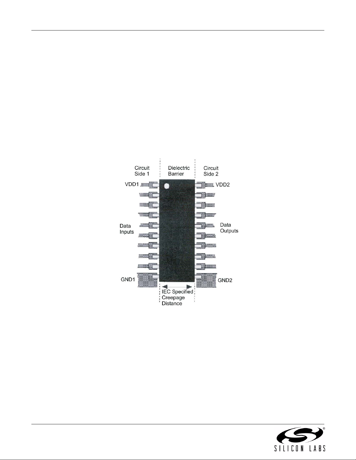
4. Layout Recommendations
Dielectric isolation is a set of specifications produced by the safety regulatory agencies from around the world that
describes the physical construction of electrical equipment that derives power from a high-voltage power system
such as 100–240 V
specifications places a very high voltage between the input power pins of a product and the user circuits and the
user touchable surfaces of the product. For the IEC relating to products deriving their power from the 220–240 V
power grids, the test voltage is 2500 V
There are two terms described in the safety specifications:
Creepage—the distance along the insulating surface an arc may travel.
Clearance—the distance through the shortest path through air that an arc may travel.
Figure 13 illustrates the accepted method of providing the proper creepage distance along the surface. For a
220–240 V application, this distance is 8 mm and the wide body SOIC package must be used. There must be no
copper traces within this 8 mm exclusion area, and the surface should have a conformal coating such as solder
resist. The digital isolator chip must straddle this exclusion area.
systems or industrial power systems. The dielectric test (or HIPOT test) given in the safety
AC
(or 3750 VDC—the peak equivalent voltage).
AC
Figure 13. Creepage Distance
4.1. Supply Bypass
The Si843x requires a 0.1 µF bypass capacitor between V
should be placed as close as possible to the package.
20 Rev. 0.31
and GND1 and V
DD1
and GND2. The capacitor
DD2

Si8430/31/35
4.2. Input and Output Characteristics
The Si843x inputs and outputs are standard CMOS drivers/receivers. The Si844x inputs and outputs are standard
CMOS drivers/receivers. Table 12 details powered and unpowered operation of the Si84xx.
Table 12. Si84xx Operation Table
VI
Input
1,2
Input
EN
1,2,3,4
VDDI
State
1,5,6
VDDO
State
1,5,6
VO
Output
Comments
1,2
H H or NC P P H Enabled, normal operation.
LH or NC P P L
X L P P Hi-Z Disabled
X H or NC UP P L Upon the transition of VDDI from unpowered to
powered, V
returns to the same state as VI in
O
less than 1 µs.
X L UP P Hi-Z Disabled
X X P UP L Upon the transition of VDDI from unpowered to
powered, V
returns to the same state as VI in
O
less than 1 µs, if EN is in either the H or NC state.
Notes:
1. VDDI and VDDO are the input and output power supplies. V
is the enable control input located on the same output side.
2. X = not applicable; H = Logic High; L = Logic Low; Hi-Z = High Impedance.
3. It is recommended that the enable inputs be connected to an external logic high or low level when the Si84xx is
operating in noisy environments.
4. No Connect (NC) replaces EN1 on Si8430/35. No Connect replaces EN2 on the Si8435. No Connects are not internally
connected and can be left floating, tied to VDD, or tied to GND.
5. "Powered" state (P) is defined as 2.375 V < VDD < 5.5 V.
6. "Unpowered" state (UP) is defined as VDD = 0 V.
and VO are the respective input and output terminals. EN
I
Rev. 0.31 21

Si8430/31/35
4.3. Enable (EN1, EN2) Inputs
Enable inputs EN1 and EN2 can be used for multiplexing, for clock sync, or other output control. EN1, EN2 logic
operation is summarized for each isolator product in Table 13. These inputs are internally pulled-up to local VDD by
a 9 µA current source allowing them to be connected to an external logic level (high or low) or left floating. To
minimize noise coupling, do not connect circuit traces to EN1 or EN2 if they are left floating. If EN1, EN2 are
unused, it is recommended they be connected to an external logic level, especially if the Si84xx is operating in a
noisy environment.
Table 13. Enable Input Truth Table
P/N EN1* EN2* Operation
Si8430 — H Outputs B1, B2, B3 are enabled.
— L Outputs B1, B2, B3 are disabled and in high impedance state.
Si8431 H X Output A3 enabled.
L X Output A3 disabled and in high impedance state.
X H Outputs B1, B2 are enabled.
X L Outputs B1, B2 are disabled and in high impedance state.
Si8435 — — Outputs B1, B2, B3 are enabled.
*Note: X = not applicable; H = Logic High; L = Logic Low.
22 Rev. 0.31

Si8430/31/35
4.4. RF Radiated Emissions
The Si8430 family uses a RF carrier frequency of approximately 2.1 GHz. This will result in a small amount of
radiated emissions at this frequency and its harmonics. The radiation is not from the IC chip but due to a small
amount of RF energy driving the isolated ground planes which can act as a dipole antenna.
The unshielded Si8430 evaluation board passes FCC requirements. Table 14 shows measured emissions
compared to FCC requirements.
Radiated emissions can be reduced if the circuit board is enclosed in a shielded enclosure or if the PCB is a less
efficient antenna.
Table 14. Radiated Emissions
Frequency
(GHz)
2.094 70.0 74.0 –4.0
2.168 68.3 74.0 –5.7
4.210 61.9 74.0 –12.1
4.337 60.7 74.0 –13.3
6.315 58.3 74.0 –15.7
6.505 60.7 74.0 –13.3
8.672 45.6 74.0 –28.4
Measured
(dBµV/m)
FCC Spec
(dBµV/m)
Compared
to Spec
(dB)
Rev. 0.31 23

Si8430/31/35
4.5. RF Immunity and Common Mode Transient Immunity
The Si8430 family has very high common mode transient immunity while transmitting data. This is typically
measured by applying a square pulse with very fast rise/fall times between the isolated grounds. Measurements
show no failures up to 30 kV/µs. During a high surge event the output may glitch low for up to 20–30 ns, but the
output corrects immediately after the surge event.
The Si843x family passes the industrial requirements of CISPR24 for RF immunity of 3 V/m using an unshielded
evaluation board. As shown in Figure 14, the isolated ground planes form a parasitic dipole antenna, while
Figure 15 shows the RMS common mode voltage versus frequency above which the Si843x becomes susceptible
to data corruption. To avoid compromising data, care must be taken to keep RF common-mode voltage below the
envelope specified in Figure 15. The PCB should be laid-out to not act as an efficient antenna for the RF frequency
of interest. RF susceptibility is also significantly reduced when the end system is housed in a metal enclosure, or
otherwise shielded.
GND1 GND2
Isolator
Dipole
Antenna
Figure 14. Dipole Antenna
5
4
3
2
1
RMS Voltage (V)
0
500 1000 1500 2000
Frequency (MHz)
Figure 15. RMS Common Mode Voltage vs. Frequency
24 Rev. 0.31

5. Pin Descriptions
Si8430/31/35
V
DD1
GND1
A1
A2
A3
NC
EN1/NC
GND1
1
2
3
4
5
6
7
8
16
15
14
13
12
11
10
Top View
9
V
DD2
GND2
B1
B2
B3
NC
EN2/NC
GND2
Wide Body SOIC
Name SOIC-16 Pin# Type Description
V
DD1
GND1 2 Ground Side 1 ground.
A1 3 Digital Input Side 1 digital input.
A2 4 Digital Input Side 1 digital input.
A3 5 Digital I/O Side 1 digital input or output.
NC 6 NA No Connect.
1 Supply Side 1 power supply.
EN1/NC* 7 Digital Input Side 1 active high enable. NC on Si8430/35
GND1 8 Ground Side 1 ground.
GND2 9 Ground Side 2 ground.
EN2/NC* 10 Digital Input Side 2 active high enable. NC on Si8435.
NC 11 NA No Connect.
B3 12 Digital I/O Side 2 digital input or output.
B2 13 Digital Output Side 2 digital output.
B1 14 Digital Output Side 2 digital output.
GND2 15 Ground Side 2 ground.
V
DD2
*Note: No Connect. These pins are not internally connected. They can be left floating, tied to VDD or tied to GND.
16 Supply Side 2 power supply.
Rev. 0.31 25
Si8430/31/35
6. Ordering Guide
Ordering Part
Number
Si8430-A-IS 3 0 1 –40 to 125 °C SOIC-16
Si8430-B-IS 3 0 10 –40 to 125 °C SOIC-16
Si8430-C-IS 3 0 150 –40 to 125 °C SOIC-16
Si8431-A-IS 2 1 1 –40 to 125 °C SOIC-16
Si8431-B-IS 2 1 10 –40 to 125 °C SOIC-16
Si8431-C-IS 2 1 150 –40 to 125 °C SOIC-16
Si8435-B-IS 3 0 10 –40 to 125 °C SOIC-16
Note: All packages are Pb-free and RoHS Compliant. Moisture sensitivity level is MSL3 with peak reflow temperature of
260 °C according to the JEDEC industry standard classifications, and peak solder temperature.
Number of Inputs
V
Side
DD1
Number of Inputs
V
Side
DD2
Maximum
Data Rate
Temperature Package
Typ e
26 Rev. 0.31
Si8430/31/35
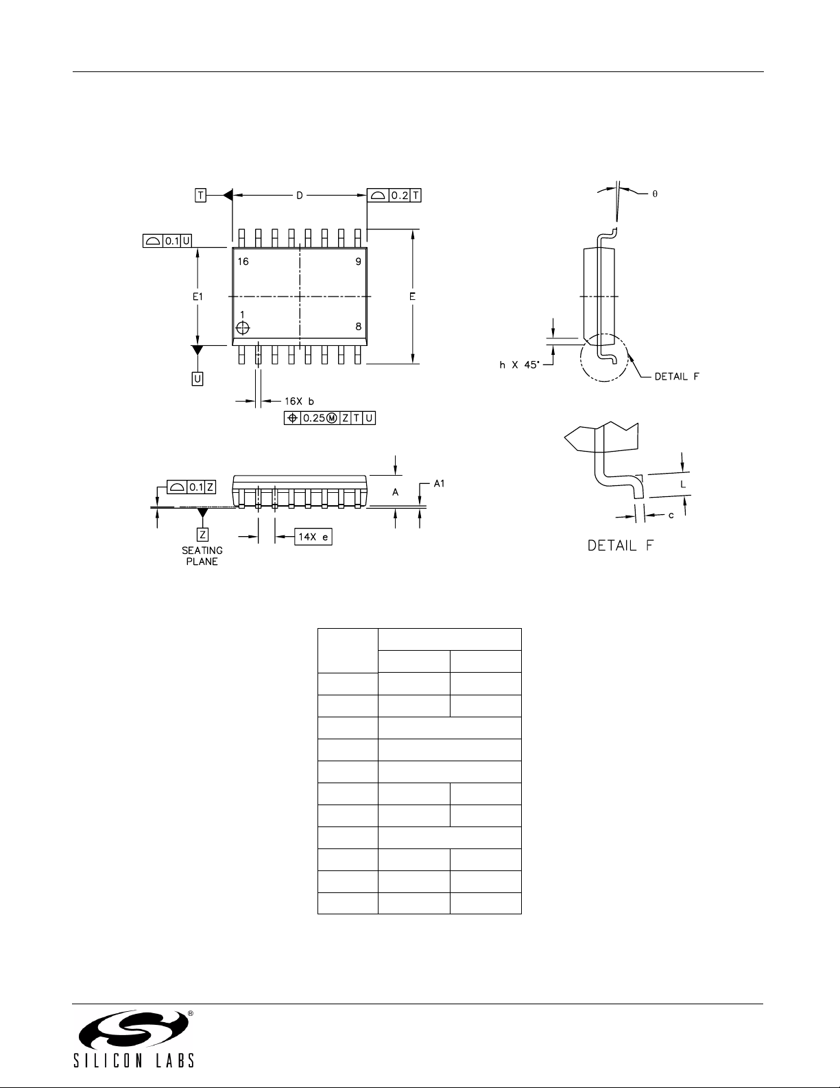
7. Package Outline: Wide Body SOIC
Figure 16 illustrates the package details for the Quad-Channel Digital Isolator. Table 14 lists the values for the
dimensions shown in the illustration.
Figure 16. 16-Pin Wide Body SOIC
Table 14. Package Diagram Dimensions
Millimeters
Symbol
A — 2.65
A1 0.1 0.3
D 10.3 BSC
E 10.3 BSC
E1
b 0.31 0.51
c 0.20 0.33
e 1.27 BSC
h 0.25 0.75
L 0.4 1.27
θ 0° 7°
Min Max
7.5 BSC
Rev. 0.31 27

Si8430/31/35
DOCUMENT CHANGE LIST
Revision 0.1 to Revision 0.11
Updated Table 7, “Regulatory Information,” on
page 14.
Minor typographical edits.
Revision 0.11 to Revision 0.2
Updated Supply Current specifications in Table 1,
“Electrical Characteristics,” on page 4, Table 2,
“Electrical Characteristics,” on page 7, and Table 3,
“Electrical Characteristics,” on page 10.
Updated performance plots in Figures 4, 5, 6, and 7.
Added NC note (Note 3) to Table 10, “Si84xx Truth
Table (Positive Logic),” on page 16.
Added NC note (*) to "5. Pin Descriptions" on page
25.
Revision 0.2 to Revision 0.3
Updated Notes to Tables 1, 2, & 3.
Updated Figure 2.
Updated Tables 6–11 to clarify specifications, test
limits, & device characteristics.
Revision 0.3 to Revision 0.31
Changed MSL2 to MSL3 in the "6. Ordering Guide"
on page 26.
28 Rev. 0.31

NOTES:
Si8430/31/35
Rev. 0.31 29

Si8430/31/35
CONTACT INFORMATION
Silicon Laboratories Inc.
400 West Cesar Chavez
Austin, TX 78701
Tel: 1+(512) 416-8500
Fax: 1+(512) 416-9669
Toll Free: 1+(877) 444-3032
Email: PowerProducts@silabs.com
Internet: www.silabs.com
The information in this document is believed to be accurate in all respects at the time of publication but is subject to change without notice.
Silicon Laboratories assumes no responsibility for errors and omissions, and disclaims responsibility for any consequences resulting from
the use of information included herein. Additionally, Silicon Laboratories assumes no responsibility for the functioning of undescribed features
or parameters. Silicon Laboratories reserves the right to make changes without further notice. Silicon Laboratories makes no warranty, representation or guarantee regarding the suitability of its products for any particular purpose, nor does Silicon Laboratories assume any liability
arising out of the application or use of any product or circuit, and specifically disclaims any and all liability, including without limitation consequential or incidental damages. Silicon Laboratories products are not designed, intended, or authorized for use in applications intended to
support or sustain life, or for any other application in which the failure of the Silicon Laboratories product could create a situation where personal injury or death may occur. Should Buyer purchase or use Silicon Laboratories products for any such unintended or unauthorized application, Buyer shall indemnify and hold Silicon Laboratories harmless against all claims and damages.
Silicon Laboratories and Silicon Labs are trademarks of Silicon Laboratories Inc.
Other products or brandnames mentioned herein are trademarks or registered trademarks of their respective holders.
30 Rev. 0.31
 Loading...