


Silicon Laboratories Si8410, Si8420, Si8421 User Manual

Si8410/20/21
LOW-POWER SINGLE AND DUAL-CHANNEL
D
IGITAL ISOLATORS
Features
High-speed operation
DC to 150 Mbps
No start-up initialization required
Wide Operating Supply Voltage:
2.70–5.5 V
Ultra low power (typical)
5 V Operation:
< 2.1 mA per channel at 1 Mbps
< 6 mA per channel at 100 Mbps
2.70 V Operation:
< 1.8 mA per channel at 1 Mbps
< 4 mA per channel at 100 Mbps
High electromagnetic immunity
Applications
Industrial automation systems
Hybrid electric vehicles
Isolated switch mode supplies
Safety Regulatory Approvals
UL 1577 recognized
Up to 2500 V
CSA component notice 5A
approval
IEC 60950-1, 61010-1
(reinforced
for 1 minute
RMS
Not Recommended
insulation)
Up to 2500 V
60-year life at rated working
voltage
Precise timing (typ ica l)
<10 ns worst case
1.5 ns pulse width distortion
0.5 ns channel-channel skew
2 ns propagation delay skew
6 ns minimum pulse width
Transient Immunity 25 kV/µs
Wide temperature range
–40 to 125 °C at 150 Mbps
RoHS-compliant packages
SOIC-8 narrow body
Isolated ADC, DAC
Motor control
Power inverters
Communications systems
RMS
isolation
w
e
VDE certification conformity
IEC 60747-5-2
(VDE0884 Part 2)
r N
o
f
e
D
g
si
s
n
Ordering Information:
See page 25.
Description
Silicon Lab's family of ultra-low-power digital isolators are CMOS devices
offering substantial data rate, propagation delay, power, size, reliability,
and external BOM advantages when compared to legacy isolation
technologies. The operating parameters of these products remain stable
across wide temperature rang es through out their service life. For ease of
design, only VDD bypass capacitors are required.
Data rates up to 150 Mbps are supported, and all devices achieve worstcase propagation delays of less than 10 ns. All products are safety
certified by UL, CSA, and VDE and support withstand voltages of up to
2.5 kVrms. These devices are available in an 8-pin narrow-body SOIC
package.
Rev. 1.5 9/13 Copyright © 2013 by Silicon Laboratories Si8410/20/21

Si8410/20/21
s
n
g
si
e
D
w
e
r N
Not Recommended
o
f
2 Rev. 1.5

Si8410/20/21
TABLE OF CONTENTS
Section Page
1. Electrical Specifications . . . . . . . . . . . . . . . . . . . . . . . . . . . . . . . . . . . . . . . . . . . . . . . . . . .4
2. Functional Description . . . . . . . . . . . . . . . . . . . . . . . . . . . . . . . . . . . . . . . . . . . . . . . . . . .17
2.1. Theory of Operation . . . . . . . . . . . . . . . . . . . . . . . . . . . . . . . . . . . . . . . . . . . . . . . . .17
2.2. Eye Diagram . . . . . . . . . . . . . . . . . . . . . . . . . . . . . . . . . . . . . . . . . . . . . . . . . . . . . . .18
2.3. Device Operation . . . . . . . . . . . . . . . . . . . . . . . . . . . . . . . . . . . . . . . . . . . . . . . . . . .19
2.4. Layout Recommendations . . . . . . . . . . . . . . . . . . . . . . . . . . . . . . . . . . . . . . . . . . . .20
2.5. Typical Performance Characteristics . . . . . . . . . . . . . . . . . . . . . . . . . . . . . . . . . . . .21
3. Errata and Design Migration Guidelines . . . . . . . . . . . . . . . . . . . . . . . . . . . . . . . . . . . . .23
3.1. Power Supply Bypass Capacitors (Revision C and Revision D) . . . . . . . . . . . . . . . .23
3.2. Latch Up Immunity (Revision C Only) . . . . . . . . . . . . . . . . . . . . . . . . . . . . . . . . . . . .23
4. Pin Descriptions . . . . . . . . . . . . . . . . . . . . . . . . . . . . . . . . . . . . . . . . . . . . . . . . . . . . . . . . .24
5. Ordering Guide . . . . . . . . . . . . . . . . . . . . . . . . . . . . . . . . . . . . . . . . . . . . . . . . . . . . . . . . . .25
6. Package Outline: 8-Pin Narrow Body SOIC . . . . . . . . . . . . . . . . . . . . . . . . . . . . . . . . . . .26
7. Land Pattern: 8-Pin Narrow Body SOIC . . . . . . . . . . . . . . . . . . . . . . . . . . . . . . . . . . . . . .27
8. Top Marking: 8-Pin Narrow Body SOIC . . . . . . . . . . . . . . . . . . . . . . . . . . . . . . . . . . . . . .28
8.1. 8-Pin Narrow Body SOIC Top Marking . . . . . . . . . . . . . . . . . . . . . . . . . . . . . . . . . . .28
8.2. Top Marking Explanation . . . . . . . . . . . . . . . . . . . . . . . . . . . . . . . . . . . . . . . . . . . . .28
Document Change List . . . . . . . . . . . . . . . . . . . . . . . . . . . . . . . . . . . . . . . . . . . . . . . . . . . . .29
Contact Information . . . . . . . . . . . . . . . . . . . . . . . . . . . . . . . . . . . . . . . . . . . . . . . . . . . . . . . .30
e
g
si
s
n
D
w
e
r N
Not Recommended
o
f
Rev. 1.5 3

Si8410/20/21
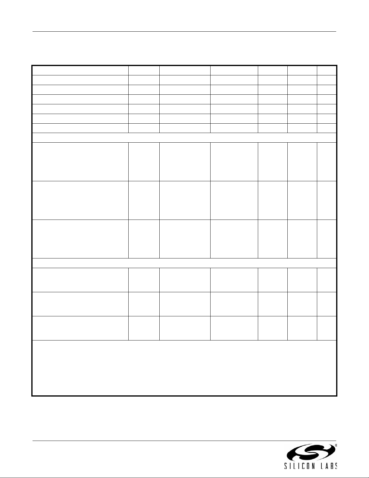
1. Electrical Specifications
Table 1. Recommended Operating Conditions
Parameter Symbol Test Condition Min Typ Max Unit
Ambient Operating Temperature* T
Supply Voltage V
*Note: The maximum ambient temperatur e is dependent upon data frequency, output loading, the number of operating
channels, and supply voltage.
Table 2. Absolute Maximum Ratings
Parameter Symbol Min Typ Max Unit
Storage Temperature
Operating Temperature T
Supply Voltage (Revision C)
Supply Voltage (Revision D)
Input Voltage V
Output Voltage V
Output Current Drive Channel I
Lead Solder Temperature (10 s) — — 260 °C
Maximum Isolation Voltage (1 s) — — 3600 V
Notes:
1. Permanent device damage may occur if the absolute maximum ratings are exceeded. Functional operation should be
restricted to conditions as specified in the operational sections of this data sheet.
2. VDE certifies storage temperature from –40 to 150 °C.
3. See "5. Ordering Guide" on page 25 for more information.
2
3
3
V
A
DD1
DD2
150 Mbps, 15 pF, 5 V –40 25 125 °C
2.70 — 5.5 V
2.70 — 5.5 V
1
V
V
T
DD1
DD1
STG
A
, V
, V
I
O
O
DD2
DD2
–65 — 150 °C
–40 — 125 °C
–0.5 — 5.75 V
–0.5 — 6.0 V
s
n
g
–0.5 — VDD + 0.5 V
si
–0.5 — VDD + 0.5 V
——10mA
e
D
w
e
RMS
Not Recommended
r N
o
f
4 Rev. 1.5

Si8410/20/21
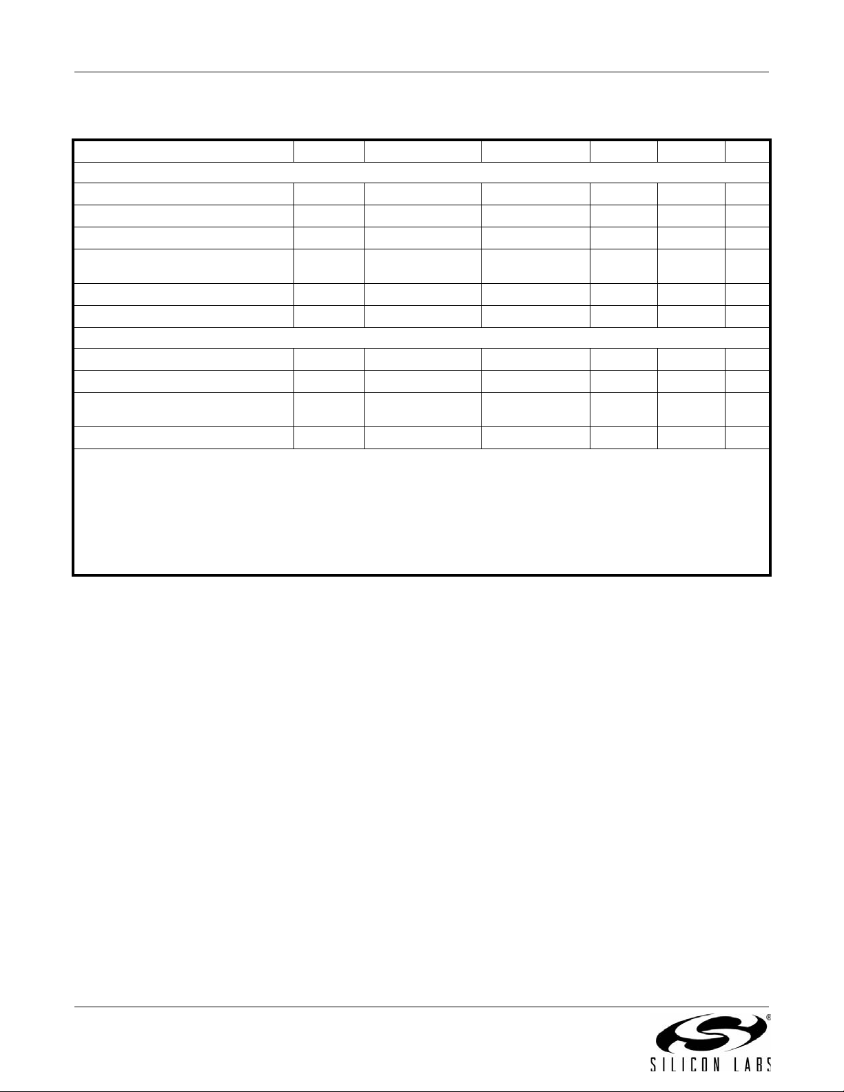
Table 3. Electrical Characteristics
(V
= 5 V ±10%, V
DD1
Parameter Symbol Test Condition Min Typ Max Unit
High Level Input Volt age V
Low Level Input Voltage V
High Level Output Voltage V
Low Level Output Voltage V
Input Leakage Current I
Output Impedance
Si8410Ax, Bx
V
DD1
V
DD2
V
DD1
V
DD2
Si8420Ax, Bx
V
DD1
V
DD2
V
DD1
V
DD2
Si8421Ax, Bx
V
DD1
V
DD2
V
DD1
V
DD2
1 Mbps Supply Current (All inputs= 500 kHz square wave, CI = 15 pF on all outputs)
Si8410Ax, Bx
V
DD1
V
DD2
Si8420Ax, Bx
V
DD1
V
DD2
Si8421Ax, Bx
V
DD1
V
DD2
Notes:
1. The nominal output impedance of an isolator driver channel is approximately 85 , ±40%, which is a combination of
the value of the on-chip series termination resistor and channel resistance of the output driver FET . When driving loads
where transmission line effects will be a factor, output pins should be appropriately terminated with controlled
impedance PCB traces.
2. t
PSK(P-P)
the same supply voltages, load, and ambient temperature.
3. Start-up time is the time period from the application of power to valid data at the output.
is the magnitude of the difference in propagation delay times measured between different units operating at
= 5 V ±10%, TA=–40 to 125ºC)
DD2
IH
IL
OH
OL
1
L
Z
O
DC Supply Current (All inputs 0 V or at Supply)
loh = –4 mA V
lol = 4 mA — 0.2 0.4 V
All inputs 0 DC
All inputs 0 DC
All inputs 1 DC
All inputs 1 DC
2.0 — — V
——0.8V
DD1,VDD2
–0.4 4.8 — V
——±10µA
—85—
—
—
—
—
0.8
0.8
1.8
0.8
1.2
1.2
2.7
1.2
s
All inputs 0 DC
All inputs 0 DC
All inputs 1 DC
All inputs 1 DC
—
—
—
—
n
g
1.0
1.3
3.0
1.4
1.5
2.0
4.5
2.1
si
All inputs 0 DC
All inputs 0 DC
All inputs 1 DC
All inputs 1 DC
D
—
e
—
—
—
1.3
1.3
2.3
2.3
2.0
2.0
3.5
3.5
w
e
r N
—
—
—
—
1.3
0.9
2.0
1.6
2.0
1.4
3.0
2.4
Not Recommended
o
f
—
—
1.9
1.9
2.9
2.9
mA
mA
mA
mA
mA
mA
Rev. 1.5 5

Si8410/20/21
Table 3. Electrical Characteristics (Continued)
(V
= 5 V ±10%, V
DD1
Parameter Symbol Test Condition Min Typ Max Unit
10 Mbps Supply Current (All inputs = 5 MHz square wave, CI = 15 pF on all outputs)
Si8410Bx
V
DD1
V
DD2
Si8420Bx
V
DD1
V
DD2
Si8421Bx
V
DD1
V
DD2
100 Mbps Supply Current (All inputs = 50 MHz square wave, CI = 15 pF on all outputs)
Si8410Bx
V
DD1
V
DD2
Si8420Bx
V
DD1
V
DD2
Si8421Bx
V
DD1
V
DD2
Si8410Ax, Si8420Ax, Si8421Ax
Maximum Data Rate 0 — 1.0 Mbps
Minimum Pulse Width — — 250 ns
Propagation Delay t
Pulse Width Distortion
|t
PLH - tPHL
Propagation Delay Skew
Channel-Channel Skew t
Notes:
1. The nominal output impedance of an isolator driver channel is approximately 85 , ±40%, which is a combination of
2. t
3. Start-up time is the time period from the application of power to valid data at the output.
|
the value of the on-chip series termination resistor and channel resistance of the output driver FET . When driving loads
where transmission line effects will be a factor, output pins should be appropriately terminated with controlled
impedance PCB traces.
PSK(P-P)
the same supply voltages, load, and ambient temperature.
is the magnitude of the difference in propagation delay times measured between different units operating at
= 5 V ±10%, TA=–40 to 125ºC)
DD2
—
—
—
—
—
—
—
—
1.3
1.2
2.0
2.1
2.2
2.2
1.4
4.6
s
2.0
1.8
3.0
3.2
3.3
3.3
2.1
5.8
mA
mA
mA
mA
n
Timing Characteristics
—
—
si
—
—
e
g
2.2
9.2
5.8
5.8
3.3
11.5
7.3
7.3
mA
mA
D
w
, t
PHL
PLH
PWD See Figure 1 — — 25 ns
2
Not Recommended
t
PSK(P-P)
PSK
See Figure 1 — — 35 ns
e
— — 40 ns
r N
— — 35 ns
o
f
6 Rev. 1.5

Si8410/20/21
Typical
Input
t
PLH
t
PHL
Typical
Output
t
r
t
f
90%
10%
90%
10%
1.4 V
1.4 V
Table 3. Electrical Characteristics (Continued)
(V
= 5 V ±10%, V
DD1
Parameter Symbol Test Condition Min Typ Max Unit
Si8410Bx, Si8420Bx, Si8421Bx
Maximum Data Rate 0 — 150 Mbps
Minimum Pulse Width — — 6.0 ns
Propagation Delay t
Pulse Width Distortion
|t
PLH - tPHL
Propagation Delay Skew
Channel-Channel Skew t
All Models
Output Rise Time t
Output Fall Time t
Common Mode Transient
Immunity
Start-up Time
Notes:
1. The nominal output impedance of an isolator driver channel is approximately 85 , ±40%, which is a combination of
2. t
3. Start-up time is the time period from the application of power to valid data at the output.
|
3
the value of the on-chip series termination resistor and channel resistance of the output driver FET . When driving loads
where transmission line effects will be a factor, output pins should be appropriately terminated with controlled
impedance PCB traces.
PSK(P-P)
the same supply voltages, load, and ambient temperature.
is the magnitude of the difference in propagation delay times measured between different units operating at
= 5 V ±10%, TA=–40 to 125ºC)
DD2
, t
PHL
PLH
PWD See Figure 1 — 1.5 2.5 ns
2
t
PSK(P-P)
PSK
r
f
CMTI V
t
SU
See Figure 1 3.0 6.0 9.5 ns
—2.03.0ns
—0.51.8ns
CL= 15 pF — 3.8 5.0 ns
CL= 15 pF — 2.8 3.7 ns
I=VDD
or 0 V — 25 — kV/µs
—1540µs
s
n
g
si
e
D
w
e
r N
Not Recommended
o
f
Figure 1. Propagation Delay Timing
Rev. 1.5 7
Si8410/20/21
Table 4. Electrical Characteristics
(V
= 3.3 V ±10%, V
DD1
Parameter Symbol Test Condition Min Typ Max Unit
High Level Input Voltage
Low Level Input Voltage
High Level Output Voltage
Low Level Output Voltage
Input Leakage Current
Output Impedance
Si8410Ax, Bx
V
DD1
V
DD2
V
DD1
V
DD2
Si8420Ax, Bx
V
DD1
V
DD2
V
DD1
V
DD2
Si8421Ax, Bx
V
DD1
V
DD2
V
DD1
V
DD2
1 Mbps Supply Current (All inputs = 500 kHz square wave, CI = 15 pF on all outputs)
Si8410Ax, Bx
V
DD1
V
DD2
Si8420Ax, Bx
V
DD1
V
DD2
Si8421Ax, Bx
V
DD1
V
DD2
Notes:
1. The nominal output impedance of an isolator driver channel is approximately 85 , ±40%, which is a combination of the
value of the on-chip series termination resistor and channel resistance of the output driver FET. When driving loads
where transmission line effects will be a factor, output pins should be appropriately terminated with controlled
impedance PCB traces.
2. t
PSK(P-P)
the same supply voltages, load, and ambient temperature.
3. Start-up time is the time period from the application of power to valid data at the output.
is the magnitude of the difference in propagation delay times measured between different units operating at
= 3.3 V ±10%, TA= –40 to 125 °C)
DD2
V
IH
V
IL
V
OH
V
OL
I
1
DC Supply Current (All inputs 0 V or at supply)
L
Z
O
loh = –4 mA V
lol = 4 mA — 0.2 0.4 V
All inputs 0 DC
All inputs 0 DC
All inputs 1 DC
All inputs 1 DC
All inputs 0 DC
All inputs 0 DC
All inputs 1 DC
All inputs 1 DC
All inputs 0 DC
All inputs 0 DC
All inputs 1 DC
All inputs 1 DC
D
2.0 — — V
——0.8V
DD1,VDD2
e
–0.4 3.1 — V
——±10µA
—85—
—
—
—
—
—
—
—
—
si
—
—
—
—
n
g
0.8
0.8
1.8
0.8
1.0
1.3
3.0
1.4
1.3
1.3
2.3
2.3
s
1.2
1.2
2.7
1.2
1.5
2.0
4.5
2.1
2.0
2.0
3.5
3.5
w
e
r N
Not Recommended
—
—
—
—
1.3
0.9
2.0
1.6
2.0
1.4
3.0
2.4
o
f
—
—
1.9
1.9
2.9
2.9
mA
mA
mA
mA
mA
mA
8 Rev. 1.5

Si8410/20/21
Table 4. Electrical Characteristics (Continued)
(V
= 3.3 V ±10%, V
DD1
Parameter Symbol Test Condition Min Typ Max Unit
10 Mbps Supply Current (All inputs = 5 MHz square wave, CI = 15 pF on all outputs)
Si8410Bx
V
DD1
V
DD2
Si8420Bx
V
DD1
V
DD2
Si8421Bx
V
DD1
V
DD2
100 Mbps Supply Current (All inputs = 50 MHz square wave, CI = 15 pF on all outputs)
Si8410Bx
V
DD1
V
DD2
Si8420Bx
V
DD1
V
DD2
Si8421Bx
V
DD1
V
DD2
Si8410Ax, Si8420Ax, Si8421Ax
Maximum Data Rate
Minimum Pulse Width
Propagation Delay
Pulse Width Distortion
|t
– t
PLH
Propagation Delay Skew
Channel-Channel Skew
Notes:
1. The nominal output impedance of an isolator driver channel is approximately 85 , ±40%, which is a combination of the
2. t
3. Start-up time is the time period from the application of power to valid data at the output.
|
PHL
value of the on-chip series termination resistor and channel resistance of the output driver FET. When driving loads
where transmission line effects will be a factor, output pins should be appropriately terminated with controlled
impedance PCB traces.
PSK(P-P)
the same supply voltages, load, and ambient temperature.
is the magnitude of the difference in propagation delay times measured between different units operating at
= 3.3 V ±10%, TA= –40 to 125 °C)
DD2
—
—
—
—
—
—
—
—
1.3
1.2
2.0
2.1
2.2
2.2
1.3
3.3
s
2.0
1.8
3.0
3.2
3.3
3.3
2.0
4.9
n
Timing Characteristics
—
—
si
—
—
e
g
2.0
6.5
4.4
4.4
3.0
8.1
5.5
5.5
D
0—1.0Mbps
w
, t
t
PHL
PLH
PWD See Figure 1 — — 25 ns
2
Not Recommended
t
PSK(P-P)
r N
t
PSK
See Figure 1 — — 35 ns
e
——250ns
— — 40 ns
— — 35 ns
o
f
mA
mA
mA
mA
mA
mA
Rev. 1.5 9
Si8410/20/21
Table 4. Electrical Characteristics (Continued)
(V
= 3.3 V ±10%, V
DD1
Parameter Symbol Test Condition Min Typ Max Unit
Si8410Bx, Si8420Bx, Si8421Bx
Maximum Data Rate
Minimum Pulse Width
Propagation Delay
Pulse Width Distortion
|t
– t
PLH
Propagation Delay Skew
Channel-Channel Skew
All Models
Output Rise Time
Output Fall Time
Common Mode Transient
Immunity
Start-up Time
Notes:
1. The nominal output impedance of an isolator driver channel is approximately 85 , ±40%, which is a combination of the
2. t
3. Start-up time is the time period from the application of power to valid data at the output.
|
PHL
3
value of the on-chip series termination resistor and channel resistance of the output driver FET. When driving loads
where transmission line effects will be a factor, output pins should be appropriately terminated with controlled
impedance PCB traces.
PSK(P-P)
the same supply voltages, load, and ambient temperature.
is the magnitude of the difference in propagation delay times measured between different units operating at
= 3.3 V ±10%, TA= –40 to 125 °C)
DD2
, t
t
PHL
PLH
PWD See Figure 1 — 1.5 2.5 ns
2
t
PSK(P-P)
t
PSK
t
r
t
f
CMTI V
t
SU
0—150Mbps
——6.0ns
See Figure 1 3.0 6.0 9.5 ns
—2.03.0ns
—0.51.8ns
CL= 15 pF — 4.3 6.1 ns
CL= 15 pF — 3.0 4.3 ns
I=VDD
or 0 V — 25 — kV/µs
—1540µs
s
n
g
si
e
D
w
e
r N
Not Recommended
o
f
10 Rev. 1.5