

Preliminary Rev. 0.8 3/06 Copyright © 2006 by Silicon Laboratories Si8250/1/2
This information applies to a product under development. Its characteristics and specifications are subject to change without notice.
Si8250/1/2
DIGITAL POWER CONTROLLER
Features
Description
Si8250/1/2 provides all control and protection functions necessary to implement
highly intelligent, fast response power delivery and management control systems
for isolated and non-isolated power supplies. On-board processing capability
enables intelligent control optimization for improved system performance and new
capabilities such as serial connectivity via the PMBus or on-board UART. The
Si8250/1/2 family is in-system Flash programmable enabling control and
protection parameters such as system regulation and protection settings, start-up
and shutdown modes, loop response, and modulation timing to be readily
modified. The built-in high-speed control path provides loop updates every 100nS
and provides pulse-by-pulse current limiting and over-current protection even
while the internal CPU is disabled.
The Si825x family is supported by the Si8250DK development kit, which contains
everything required to develop and program power supply applications with the
Si825x family of digital controllers.
Single-Chip, Flash-based digital
power controller
Supports isolated and non-isolated
applications
Enables new system capabilities
such as:
- Adaptive dead-time control for
higher efficiency
- Nonlinear control for faster
transient response
- Self diagnostics for higher
reliability
- Full PMBus command set
implementation for system
connectivity
Highly integrated control solution:
High-speed digital hardware
control loop
In-system programmable
supervisory processor
Programmable system protection
functions
Hardware cycle-by-cycle current
limiting and OCP
External clock and frame
synchronization inputs
Performs system management
functions such as external power
supply sequencing and fan
control/monitoring
In-system Flash programmable
Flash can also be used as NV
memory for data storage
Low cost, comprehensive
development tool kit includes:
Graphical, easy-to-use system
design tools
Integrated development
environment
In-system, on-line debugger
Turnkey isolated 35 W digital
half-bridge target board
Typical Applications
Isolated and non-isolated DC/DC
converters
AC/DC converters
Fully Pb-free and ROHS compliant
packages
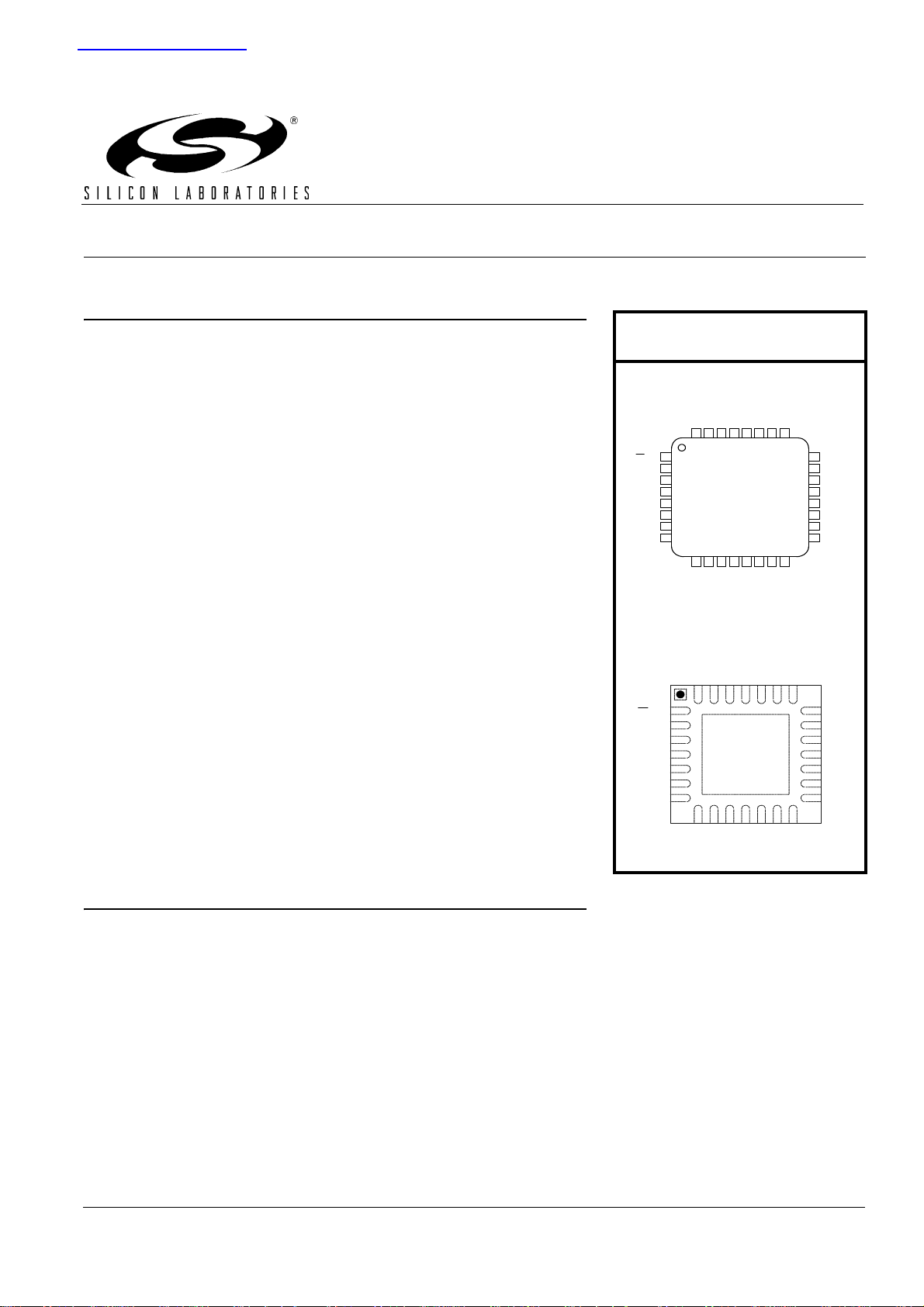
32-pin LQFP
28-pin 5 x 5 mm QFN
Temp Range: –40 to +125 ºC
Patents pending
Pin Assignments:
See page 23
4
5
6
7
2
1
3
111213
14
9
8
10
18
17
16
15
20
21
19
25
26
27
28
232224
Si8250/1/2
Top View
RST / C2CK
IPK
VSENSE
GND
VDD
VREF
P1.0/VIN/AIN0
P1.1/AIN1
P1.2/AIN2
P1.3/AIN3
P1.4/AIN4
P1.5/AIN5
P1.6/AIN6
P1.7/AIN7/C2D
P0.7
P0.6
P0.5
P0.4
P0.3/XCLK
P0.2
P0.1
P0.0
PH6
PH5
PH4
PH3
PH2
PH1
GND
GND
1
VSENSE
P0.0
P0.5
P0.2
P0.1
P0.3 / XCLK
P1.0/VIN/AIN 0
IPK
P0.6
P0.7
2
3
4
5
6
7
8
24
23
22
21
20
19
18
17
9
10111213141516
32313029282726
25
P0.4
Si8250/1/2
Top View
P1.1/AIN1
GNDA
VDDA
RST/C2CK
GND
VDD
P1.5/AIN5
P1.6/AIN6
P1.7/AIN7/C2D
PH6
PH5
P1.4/AIN4
VDD
GND
PH3
P1.3/AIN3
P1.2/AIN2
VREF
PH4
PH2
PH1
28-pin QFN
32-pin LQFP
查询SI8250-IQ供应商

Si8250/1/2
2 Preliminary Rev. 0.8

Si8250/1/2
Preliminary Rev. 0.8 3
TABLE OF CONTENTS
Section Page
1. Electrical Specifications . . . . . . . . . . . . . . . . . . . . . . . . . . . . . . . . . . . . . . . . . . . . . . . . . . .4
2. Benefits of Digital Power Control . . . . . . . . . . . . . . . . . . . . . . . . . . . . . . . . . . . . . . . . . . . 14
3. Product Description . . . . . . . . . . . . . . . . . . . . . . . . . . . . . . . . . . . . . . . . . . . . . . . . . . . . . .15
3.1. System Operation . . . . . . . . . . . . . . . . . . . . . . . . . . . . . . . . . . . . . . . . . . . . . . . . . . .16
3.2. Control Processor Functional Block Descriptions (Figure 1) . . . . . . . . . . . . . . . . . . . 16
3.3. System Management Processor Functional Block Descriptions . . . . . . . . . . . . . . . . 17
4. Design Tools . . . . . . . . . . . . . . . . . . . . . . . . . . . . . . . . . . . . . . . . . . . . . . . . . . . . . . . . . . . .18
5. Example Applications . . . . . . . . . . . . . . . . . . . . . . . . . . . . . . . . . . . . . . . . . . . . . . . . . . . .19
6. Layout Considerations . . . . . . . . . . . . . . . . . . . . . . . . . . . . . . . . . . . . . . . . . . . . . . . . . . .21
7. Pin Descriptions—Si8250/1/2 . . . . . . . . . . . . . . . . . . . . . . . . . . . . . . . . . . . . . . . . . . . . . .23
8. Ordering Guide . . . . . . . . . . . . . . . . . . . . . . . . . . . . . . . . . . . . . . . . . . . . . . . . . . . . . . . . . . 25
9. Package Outline—32LQFP . . . . . . . . . . . . . . . . . . . . . . . . . . . . . . . . . . . . . . . . . . . . . . . .26
10. Package Outline—28QFN . . . . . . . . . . . . . . . . . . . . . . . . . . . . . . . . . . . . . . . . . . . . . . . . 27
Document Change List . . . . . . . . . . . . . . . . . . . . . . . . . . . . . . . . . . . . . . . . . . . . . . . . . . . . .28
Contact Information . . . . . . . . . . . . . . . . . . . . . . . . . . . . . . . . . . . . . . . . . . . . . . . . . . . . . . . .30
Si8250/1/2
4 Preliminary Rev. 0.8
1. Electrical Specifications
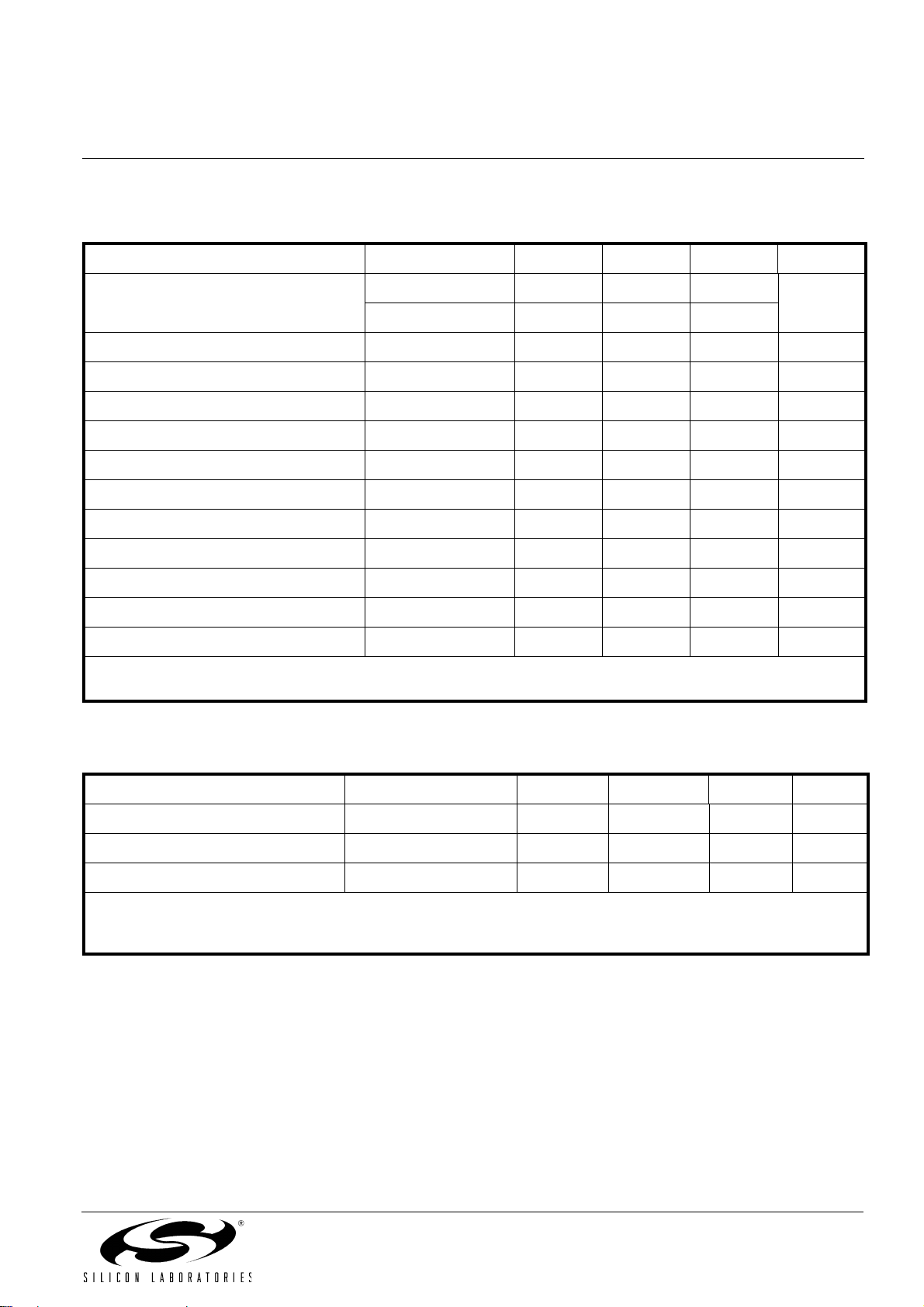
Table 1. Absolute Maximum Ratings*
Parameter Conditions Min. Typ. Max. Units
Ambient Temperature under Bias –55 — +135 °C
Storage Temperature –65 — +150 °C
Voltage on any Port0 Pin with respect to GND –0.3 — 5.5 V
Voltage on all other pins with respect to GND –0.3 — 4.0 V
Voltage on VDD with respect to GND –0.3 — 4.0 V
Maximum total current through VDD or GND — — 400 mA
Maximum output current sunk by RST
or any
Port pin
——80mA
*Note: Stresses above those listed under "2.1 Absolute Maximum Ratings" may cause permanent damage to the device. This
is a stress rating only, and functional operation of the devices at those or any other conditions above those indicated in
the operation listings of this specification is not implied. Exposure to maximum rating conditions for extended periods
may affect device reliability.
Table 2. DC Electrical Specifications
TA = –40 to +125 °C, VDD = 2.5 V, SYSCLK = 25 MHz, PLLCLK = 200 MHz unless otherwise specified.
Parameter Conditions Min Typ Max Units
Supply Voltage 2.25 — 2.75 V
Supply Current, all Peripherals
Enabled
Analog + digital supply current. — 26 — mA
Lockout mode supply current Analog + digital supply current.
(See Table 1 on page 4)
—300— µA
Digital Supply Current (shutdown) Oscillator not running, VDD mon-
itor disabled
——TBDµA
Digital Supply RAM Data Retention
Voltage
—1.5— V
Si8250/1/2
Preliminary Rev. 0.8 5
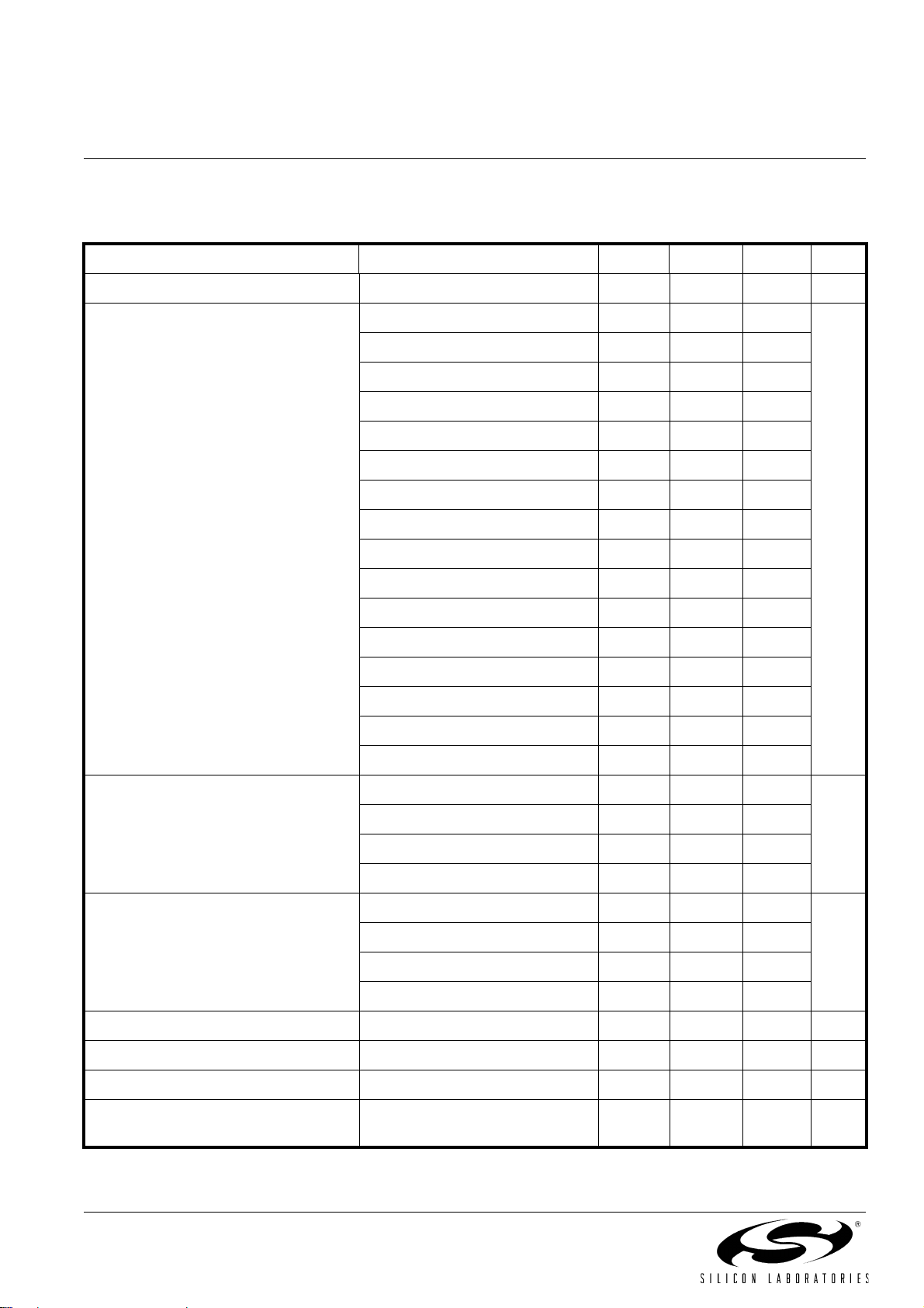
Table 3. Reference DAC Electrical Specifications
TA = –40 to +125 °C, VDD = 2.5 V, SYSCLK = 25 MHz, PLLCLK = 200 MHz unless otherwise specified.
Parameter Conditions Min Typ Max Units
Resolution — — 9 Bits
LSB Size — 2.44 — mV
Integral Nonlinearity (INL) –2 — +2 LSB
Differential Nonlinearity (DNL) –1.0 — +1.0 LSB
Settling Time 1/2 LSB change from 0 to
full scale
—2—µs
Turn-on Time — 20 — µs
Noise 2 MHz BW — 1 — mV
PP
Power Supply Rejection — 70 — db
Supply Current — 220 — µA
Shutdown Supply Current — 0.1 — µA
Si8250/1/2
6 Preliminary Rev. 0.8
Table 4. ADC0 (12-Bit ADC) Specifications
TA = –40 to +125 °C, VDD = 2.5 V, SYSCLK = 25 MHz, PLLCLK = 200 MHz unless otherwise specified.
Parameter Conditions Min Typ Max Units
DC Accuracy
Resolution — 12 — bits
Integral Nonlinearity — — ±2 LSB
Differential Nonlinearity Guaranteed Monotonic — — ±1 LSB
Offset Error — ±3 — LSB
Full Scale Error Differential mode — 3 — LSB
Offset Temperature Coefficient — TBD — ppm/°C
Dynamic Performance (10 kHz sine-wave Single-ended input, 0 to 1 dB below Full Scale, 200 ksps)
Signal-to-Noise Plus Distortion — 64 — dB
Total Harmonic Distortion Up to the 5
th
harmonic — 83 — dB
Spurious-Free Dynamic Range — –73 — dB
Conversion Rate
Conversion Time in SAR Clocks Note 1 — 13 — clocks
Track/Hold Acquisition Time Note 2 1 — — µs
Throughput Rate — — 200 ksps
Analog Inputs
Input Voltage Range 0 — V
REF
V
Input Capacitance — 15 — pF
Temperature Sensor
Linearity Notes 3, 4 — ±TBD — °C
Gain Notes 3, 4 — 1353 — µV/°C
Offset Notes 3, 4 (Temp = 0 °C) — 488 — mV
Power Specifications
Power Supply Current (V
DD
sup-
plied to ADC0)
Operating Mode, 200 ksps — 780 — µA
Power-On Time After V
REF
settle, before tracking
begins
—5— µs
Power Supply Rejection — TBD — mV/V
Notes:
1. An additional 2
F
CLK
cycles are required to start and complete a conversion.
2. Additional tracking time may be required depending on the output impedance connected to the ADC input.
3. Represents one standard deviation from the mean.
4. Includes ADC offset, gain, and linearity variations.
Si8250/1/2
Preliminary Rev. 0.8 7
Table 5. ADC1 Specifications
TA = –40 to +125 °C, VDD = 2.5 V, SYSCLK = 25 MHz, PLLCLK = 200 MHz unless otherwise specified.
Parameter Conditions Min Typ Max Units
Sampling Frequency ADCSP = 0 — 10 — Msps
ADCSP = 1 — 5 —
Resolution — — 6 Bits
LSB Size 4 — 20 mV
Differential Input Voltage Range Note 1 –32 — +31 LSB
Common-mode input voltage range 0.8 — 1.3 V
Integral Nonlinearity –2 — +2 LSB
Differential Nonlinearity –1 — +1 LSB
Gain Error — 5 — %
Offset Error — 3 — mV
Input Bias Current — 5 — µA
Standby Mode Supply Current disabled — 0.1 — µA
Operating Mode Supply Current — — 3 mA
Notes:
1. LSB size (mV) is programmable using the RES[3:0] bits in the ADC1CN register.
Table 6. DSP Filter Engine Electrical Specifications
TA = –40 to +125 °C, VDD = 2.5 V, SYSCLK = 25 MHz, PLLCLK = 200 MHz unless otherwise specified.
Parameter Conditions Min Typ Max Units
Resolution
1
——9Bits
Dithering
2
——6Bits
Standby Mode Supply Current disabled — 0.1 — µA
Notes:
1. Internal word length = 22 bits.
2. Up to a total 15 bits of resolution when dithering is enabled.
Si8250/1/2
8 Preliminary Rev. 0.8
Table 7. Peak Current Limit Detector Electrical Specifications
TA = –40 to +125 °C, VDD = 2.5 V, SYSCLK = 25 MHz, PLLCLK = 200 MHz unless otherwise specified.
Parameter Conditions Min Typ Max Units
IPK Input to DPWM Output Latency 10 mV Overdrive — 45 — ns
Threshold Detector Voltage VT[3:0] = 0000 35 50 65 mV
VT[3:0] = 0001 85 100 115
VT[3:0] = 0010 135 150 165
VT[3:0] = 0011 185 200 215
VT[3:0] = 0100 235 250 265
VT[3:0] = 0101 285 300 315
VT[3:0] = 0110 335 350 365
VT[3:0] = 0111 485 400 415
VT[3:0] = 1000 435 450 465
VT[3:0] = 1001 485 500 515
VT[3:0] = 1010 535 550 565
VT[3:0] = 1011 585 600 615
VT[3:0] = 1100 635 650 665
VT[3:0] = 1101 685 700 715
VT[3:0] = 1110 735 750 765
VT[3:0] = 1111 785 8 00 815
Hysteresis HYST[1:0] = 00 — 0 — mV
HYST[1:0] = 01 — 5 —
HYST[1:0] = 10 — 10 —
HYST[1:0] = 11 — 20 —
Blanking Time LEB[1:0] = 00, f
PLL
= 200 MHz — 0 — ns
LEB[1:0] = 01, f
PLL
=200MHz — 20 —
LEB[1:0] = 10, f
PLL
=200MHz — 40 —
LEB[1:0] = 11, f
PLL
= 200 MHz — 80 —
Input Capacitance — 4.5 — pF
Input Bias Current — 0.1 — µA
Shutdown Supply Current Enable bit = 0 — 0.1 — µA
Active Supply Current IIN = (Vt + 100 mVpp),
1.5 MHz sq. wave
—100—µA
Si8250/1/2
Preliminary Rev. 0.8 9
Table 8. DPWM Specifications
TA = –40 to +125 °C, VDD = 2.5 V, SYSCLK = 25 MHz, PLLCLK = 200 MHz unless otherwise specified.
Parameter Conditions Min Typ Max Units
Clock Frequency DPWMSP[4:3] = 00 — — 200 MHz
DPWMSP[4:3] = 01 — — 50
DPWMSP[4:3] = 1x — — 25
Resolution No dithering — — 9 Bits
Dithering enabled — — 15
Time Resolution DPWMSP[4:3] = 00 5 — — ns
DPWMSP[4:3] = 01 20 — —
DPWMSP[4:3] = 1x 40 — —
SYNC Pulse set-up time SYNC signal minimum LOW time
before positive transition
3——DPWM
clock cycles
PH Rise, Fall Time 50pF on pin — — 5 ns
Output Resistance High I
OUT
=–5mA — 75 — Ω
Output Resistance Low I
OUT
=8mA — 40 — Ω
Shutdown Supply Current — — 0.1 µA
Table 9. Bandgap Voltage Reference Specs
TA = –40 to +125 °C, VDD = 2.5 V, SYSCLK = 25 MHz, PLLCLK = 200 MHz unless otherwise specified.
Parameter Conditions Min Typ Max Units
Output Voltage — 1.20 — V
Temperature Stability –1 — +1 %
Turn-on Response (0.01%, 4.7 µF) — 6.5 — ms
no load — 2 — µs
Noise 4.7 µF — 2 — µV (RMS)
Bandgap Current — 60 — µA
Reference Buffer Current — 30 — µA
Power supply rejection — 50 — dB
 Loading...