

Silicon Laboratories Si4700, Si4701 User Manual

AN232
Si4700/01 EVALUATION BOARD USER’S GUIDE
1. Introduction—Si4700/01 EVB
Thank you for purchasing the Silicon Laboratories, Inc. Si4700/01 FM Tuner Evaluation Board (EVB). This EVB
and associated software has been designed to speed the overall development process and decrease the required
development time from EVB to product launch. We are looking forward to working with you, and have posted
support articles, answers to frequently asked questions, and application notes at https://www.mysilabs.com.
The Si4700/01 EVB kit should include the following important items:
Si4700/01 FM Tuner customer welcome and evaluation letter
Si4700/01 Errata
Si4700/01 base board Revision 1.1 (blue)
Si4700/01 daughter card with Si470x pre-mounted Revision 1.0 (red)
Wall transformer certified at 5 V/2 A, 100–240 V ac input with two jumpers (black) and
power input terminal (green)
USB cable
BNC to RCA adapters
RCA cable
Barrel adapter (1) mini jack
EVB Characterization report for included EVB
Si4700/01 Quick Start Guide
Si4700/01 CD including:
Data sheet
Development application GUI
Firmware (embedded in Development GUI)
2. Overview
The Si4700/01 Evaluation Kit includes an evaluation board (EVB) to facilitate evaluation of the Si4700/01 using the
associated software. The EVB consists of a base board (blue) with a pre-mounted daughter card (red) - the
Si4700/01 is pre-installed on the daughter card. Several input/output (I/O) connections provide access to the
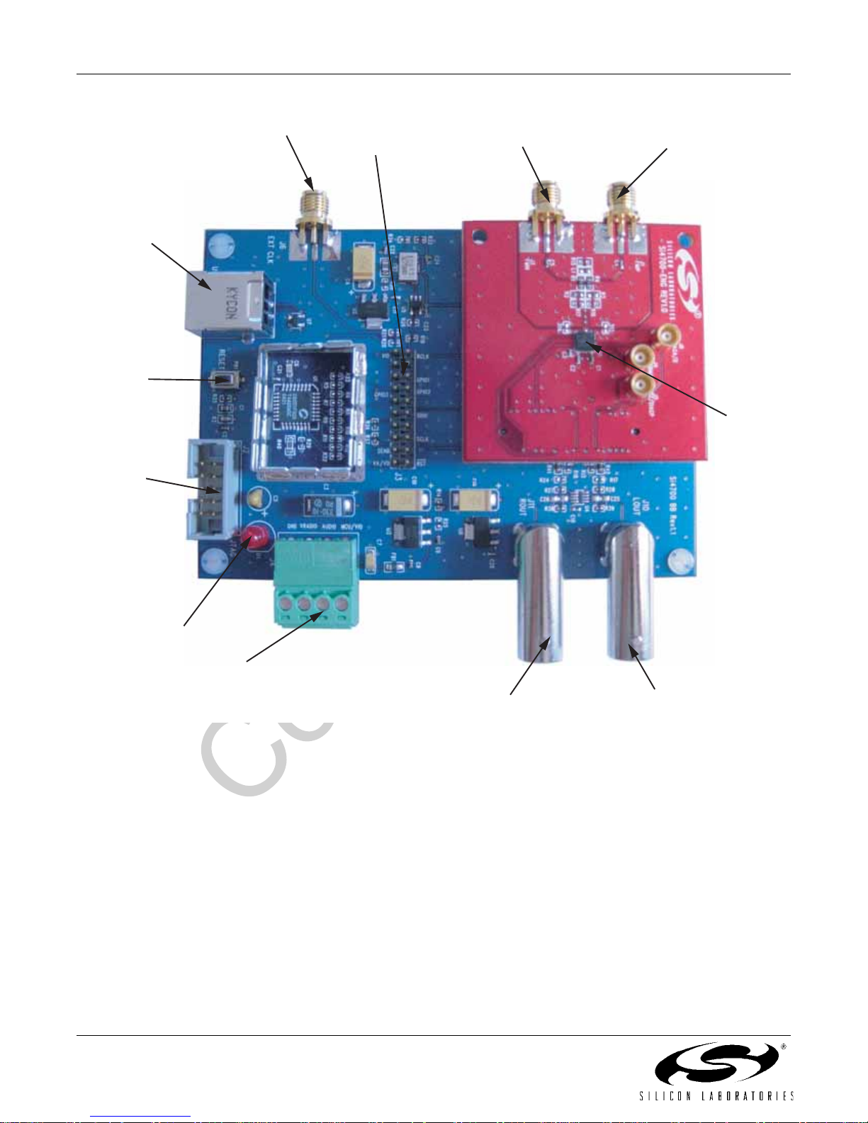
various subsystems on the EVB. Refer to Figure 1 for the locations of the various I/O connectors/devices.
3. Description
The following sections refer to both the image in Figure 1 and the silk screen on the Si4700/01 EVB. It is
recommended to refer to both when using this guide.
Rev. 0.2 5/05 Copyright © 2005 by Silicon Laboratories AN232
Silicon Laboratories Confidential. Information contained herein is covered under non-disclosure agreement (NDA).
AN232
-
3%
-
-
-
- -
8
'
-
-
Figure 1. Locations of I/O Connectors/Devices
The base board has the following I/O connectors/devices:
J1 USB connector for USB interface
J2 JTAG connector for the C8051F320 MCU
J3 20-pin Expansion I/O connector
J4 Power input terminal block
J5 Daughter card connector (not visible when the base board and daughter card are mated)
J6 SMA connector for external clock input
J10 BNC connector for left audio output
J11 BNC connector for right audio output
PB1 Push-button to reset the C8051F320 MCU
D1 LED to confirm power supply to the C8051F320 MCU
-
2 Rev. 0.2

AN232
The daughter card has the following I/O connectors/devices:
J1 SMA connector for RF (single-ended or non-inverting differential) input
J2 Base board connector (not visible when the base board and daughter card are mated)
J3 SMA connector for RF(inverting differential) input
The EVB consists of various subsystems that are explained in greater detail in the following sections.
3.1. Si4700/01 Base Board
3.1.1. Microcontroller and Associated Peripherals
The Si4700/01 evaluation environment uses a Silicon Laboratories' C8051F320 microcontroller to control the
Si4700/01 and to provide USB connectivity to the EVB (via J1). The LED D1 illuminates to confirm that power is
being properly supplied to the C8051F320 and firmware has loaded. Push-button PB1 manually resets the
C8051F320. The JTAG connector J2 is used to program the C8051F320 at production time, and is not necessary
for further development.
3.1.2. Reference Clock for the Si4700/01
The Si4700/01 accepts a 32.768 kHz reference clock input at the RCLK pin. On the EVB, this clock is provided by
a precision crystal oscillator. The output of the oscillator is routed to the Si4700/01 RCLK pin through a Schmitttrigger buffer (U5) and a 33 Ω s eries termination resistor (R19). The user has the optio n of not using the oscillator
and bringing in the reference clock from an external source through J6. This can be achieved by depopulating R19
and populating R20 with a 0 Ω resistor. Note that the reference clock is not routed through the Schmitt-trigger
buffer when an external clock source is being used.
3.1.3. Power supply network
The EVB accepts three 5 to 7 V power supplies through the power input terminal block J4. Instructions on
connecting the power input terminal can be found in "5. Hardware Setup" on page 7.
The supply labeled VMCU/VIO is the input to regulator U2. The 3.3 V output of the regulator is used to power the
microcontroller and the reference clock systems and also applied to the VIO pin of the Si4700/01. U2 may be
bypassed by depopulating U2 and populating R30 with a 0 Ω resistor. In such a case, the VMCU/VIO supply at J4
must lie between 3.0 and 3.6 V—this condition is necessary to ensure reliable operation of the C8051F320.
The supply label VAUDIO is the input to regulator U6. The 3.3 V output of U6 is used to power the audio amplifier
network.
The supply labeled VRADIO is the input to the regulator U3. The 3.3 V output of the regulator is applied to the VA
and VD pins of the Si4700/01. U3 may be bypassed by depopulating R14 and populating R25 with a 0 Ω resis tor.
In such a case, the VRADIO supply at J4 must lie between 2.7 and 5.5 V—these are the recommended operating
conditions for the Si4700/01.
3.1.4. Expansion I/O connector
The 20-pin Expansion I/O connector J3 provides access to all the control signals of the Si4700/01 including the
general purpose input/output pins. Pins for the VA, VD, VIO, and RCLK pins of the Si4700/01 are also available. All
test points on J3 are labeled indicating the signal available at the pin.
Note: The unlabeled pins on J3 between (a) SCLK and RST
system ground.
, and (b) RCLK and GPIO1, provide access to the
3.2. Si4700/01 Daughter Card
3.2.1. Si4700/01 FM Tuner Chip
The Si4700/01 (U1) and its bypass capacitors are located on the daughter card. The daughter card allows for the
implementation of different RF input networks to connect the FM inputs at J1 and J3 to the FMIP and FMIN pins of
the Si4700/01 respectively. On the EVB, the Si4700/01 is configured to accept a single-ended FM input—the FMIN
pin is grounded and the FMIP pin is connected to J1 through an ac-coupling capacitor. Refer to “AN231: Si4700/01
Headphone and Antenna Interface” for more information.
Rev. 0.2 3

AN232
3.2.2. Audio Amplifier
The EVB includes a high-output drive dual op-amp chip (U2) to buffer the audio outputs at the LOUT and ROUT
pins of the Si4700/01. U2 is located on the bottom layer of the daughter card and is not visible when the base
board and daughter card are mated. The LOUT and ROUT pins are ac-coupled to the inputs of the op-a mps on U2.
The op-amps are connected in a unity-gain, non inverting conf iguration an d biased at the m iddle of the audio p ower
supply. The outputs of the op-amps are in turn ac-coupled to the BNC connectors J10 and J11 on the base board.
The audio amplification network has been designed to drive resistances of 10 kΩ which is eas ily achievable on
most audio analyzers. The op-amps have enough drive capability to drive resistances much lower than 10 kΩ (e.g.
32 Ω headphones). In such cases, however, the lower end of the audio spectrum (up to 2.5 kHz) may get
attenuated. This is because the 3-dB points of the high-pass filte rs at the outputs of the op-a mps move to higher
frequencies as the output resistance is decreased. Also note that the op-amps are not sufficiently protected against
short-circuit conditions. Hence, the aud io outputs at J10 and J11 should not be connected to a mono input if the
Si4700/01 is configured to produce a stereo output.
4 Rev. 0.2
AN232
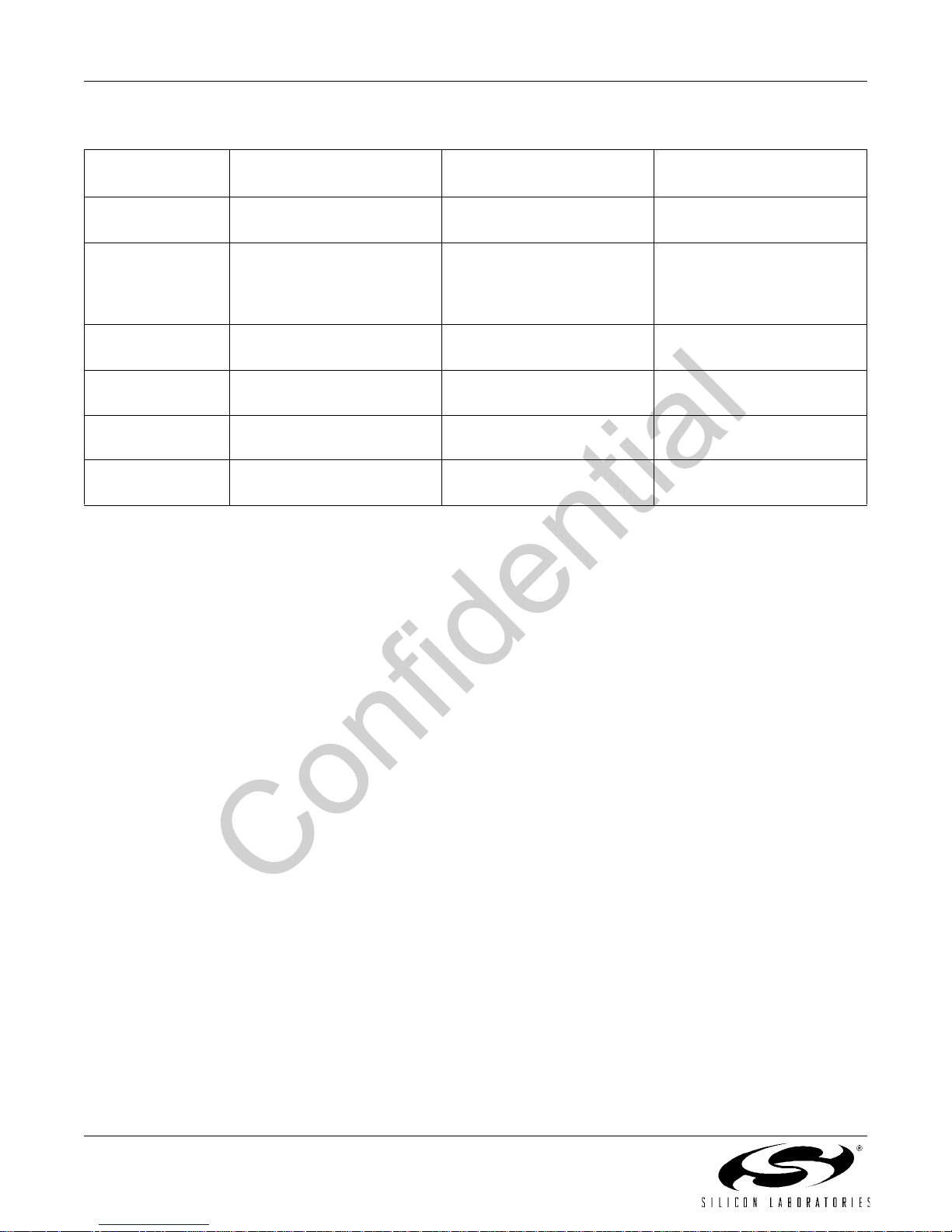
4. EVB Configuration Matrix
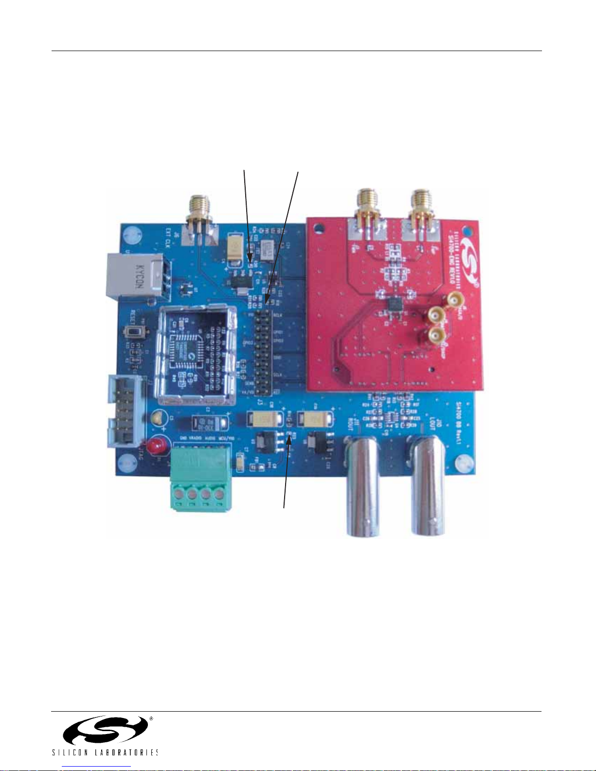
Table 1 lists the configuration options the EVB provides, the hardware changes necessary to implement a certain
option, and any associated constraints. Figure 2 shows the locations of the various components required to
configure the EVB.
58
55
Figure 2. Locations of Components Used to Configu r e the EVB
55
Rev. 0.2 5
AN232
Table 1. EVB Configuration Matrix
Configuration
Variable
Reference clock
source
Reference clock
source
VIO source Output of U2 None (default option). 5 V input at VMCU/VIO sup-
VIO source VMCU/VIO supply (U2
VA/VD source Output of U3 None (default option). 5 V input at VRADIO supply
VA/VD source VRADIO supply (U3
Value of Configuration
Variable
Crystal oscillator on EVB None (default option). None
External clock Depopulate R19. Populate
bypassed)
bypassed)
Hardware Changes Constraints
32.768 kHz, CMOS switch-
R20 with 0 Ω.
Depopulate U2. Populate
R30 with 0 Ω resistor.
Depopulate R14. Populate
R25 with 0 Ω resistor.
ing level, VIO voltage supply
from an external clock
source
ply on J4.
3.0–3.6 V input at VMCU/
VIO supply on J4
on J4
2.7–5.5 V input at VRADIO
supply on J4
6 Rev. 0.2
 Loading...