


Si4700/01/02/03-EVB
Si4700/01/02/03 EVALUATION BOARD USER’S GUIDE
1. Introduction—Si4700/01/02/03 EVB
Thank you for purchasing the Silicon Laboratories, Inc. Si4700/01/02/03 FM Tuner Evaluation Board (EVB). This
EVB and associated software have been designed to speed the overall development process and decrease the
required development time from EVB to product launch. We have posted support articles, answers to frequently
asked questions, and application notes at https://www.mysilabs.com.
The Si4700/01/02/03 EVB kit should include the following important items:
Si4700/01/02/03 FM Tuner customer welcome and evaluation letter
Si4700/01/02/03 baseboard Revision 1.2
Si4700/01/02/03 daughter card with pre-mounted Si4700/01 Revision 1.3 or Si4702/03 Revision 1.1
Wall transformer certified at 5 V/2 A, 100–240 V ac input and power input terminal (green)
USB cable
BNC to RCA adapters (2)
RCA to 1/8” jack cable
1/8” barrel adapter (1)
EVB Characterization Report
Si4700/01/02/03 Quick Start Guide
Si4700/01/02/03 CD including:
Data sheet
Development application GUI
Note: This version of the document supports the third generation of the GUI so ftware. Boards shipped prior to May 2006 may
be reprogrammed to use this new GUI. Instructions for doing so can be found on mysilabs.com. For details on the first
generation GUI, please reference the 0.2 version of this document, also available on https://www.mysilabs.com.
2. Overview
The Si4700/01/02/03 Evaluation Kit includes an evaluation board (EVB) to facilitate evaluation of the
Si4700/01/02/03 using the associated software. The EVB consists of a baseboard with a pre-mounted daughter
card. The Si4700/01/02/03 is pre-installed on the daughter card. The Si4700 and Si4701 come in a 4 x 4 mm 24pin QFN package and the Si4702 and Si4703 come in a 3 x 3 mm 20-pin QFN package. The Si4701 and Si4703
offer RDS support, while the Si4700 and Si4702 do not. Several input/output (I/O) connections provide access to
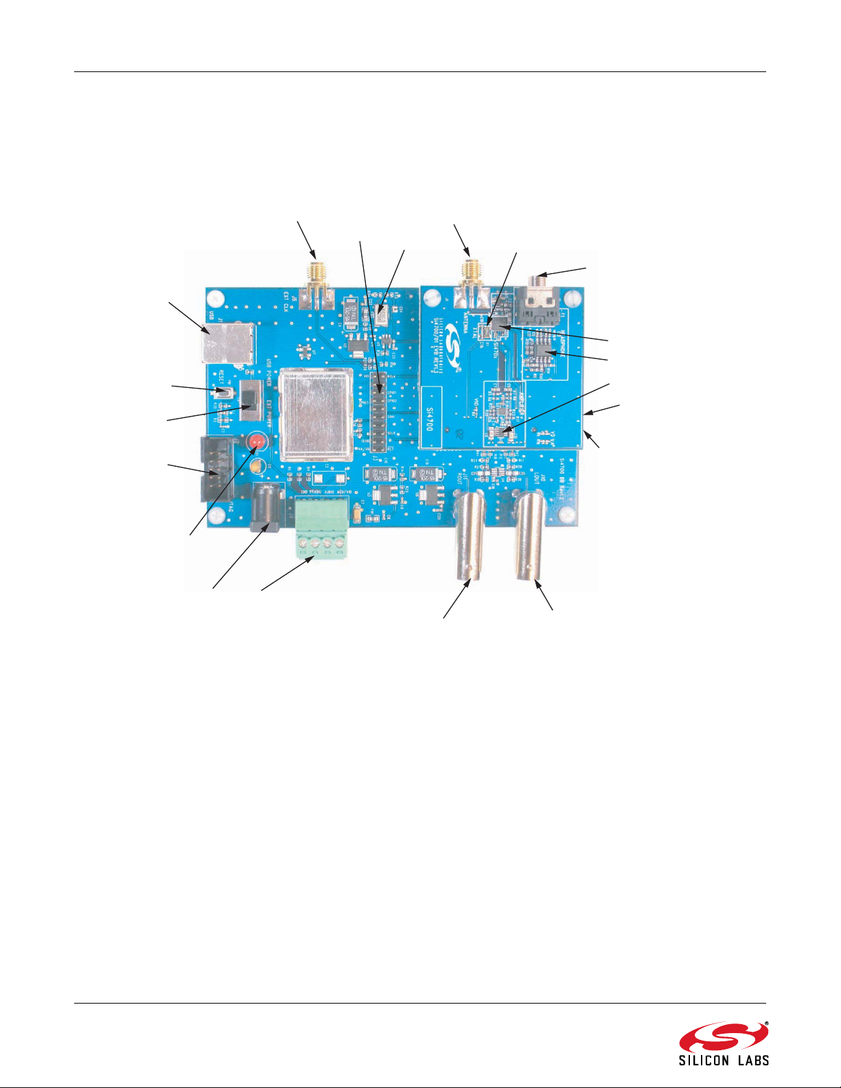
the various subsystems on the EVB. Refer to Figure 1 for the locations of the various I/O connectors/devices.
This document references the Si4700/01 data sheet and the Si4702/03 data sheet.
Rev. 0.9 1/15 Copyright © 2015 by Silicon Laboratories Si4700/01/02/03-EVB

Si4700/01/02/03-EVB
2 Rev. 0.9

Si4700/01/02/03-EVB
TABLE OF CONTENTS
Section Page
1. Introduction—Si4700/01/02/03 EVB . . . . . . . . . . . . . . . . . . . . . . . . . . . . . . . . . . . . . . . . . .1
2. Overview . . . . . . . . . . . . . . . . . . . . . . . . . . . . . . . . . . . . . . . . . . . . . . . . . . . . . . . . . . . . . . . .1
3. Description . . . . . . . . . . . . . . . . . . . . . . . . . . . . . . . . . . . . . . . . . . . . . . . . . . . . . . . . . . . . . .4
3.1. Si4700/01/02/03 Baseboard . . . . . . . . . . . . . . . . . . . . . . . . . . . . . . . . . . . . . . . . . . . .5
3.2. Si4700/01/02/03 Daughter Card . . . . . . . . . . . . . . . . . . . . . . . . . . . . . . . . . . . . . . . . .6
4. EVB Configuration Matrix . . . . . . . . . . . . . . . . . . . . . . . . . . . . . . . . . . . . . . . . . . . . . . . . . .7
5. Hardware Setup . . . . . . . . . . . . . . . . . . . . . . . . . . . . . . . . . . . . . . . . . . . . . . . . . . . . . . . . . .9
6. Getting Started—Software Installation . . . . . . . . . . . . . . . . . . . . . . . . . . . . . . . . . . . . . . .10
6.1. Connecting to the EVB . . . . . . . . . . . . . . . . . . . . . . . . . . . . . . . . . . . . . . . . . . . . . . .11
6.2. Running the Software . . . . . . . . . . . . . . . . . . . . . . . . . . . . . . . . . . . . . . . . . . . . . . . .13
7. Schematics . . . . . . . . . . . . . . . . . . . . . . . . . . . . . . . . . . . . . . . . . . . . . . . . . . . . . . . . . . . . .28
8. Layout . . . . . . . . . . . . . . . . . . . . . . . . . . . . . . . . . . . . . . . . . . . . . . . . . . . . . . . . . . . . . . . . .31
8.1. Baseboard . . . . . . . . . . . . . . . . . . . . . . . . . . . . . . . . . . . . . . . . . . . . . . . . . . . . . . . . .31
8.2. Si4700/01 Daughter Card . . . . . . . . . . . . . . . . . . . . . . . . . . . . . . . . . . . . . . . . . . . . .34
8.3. Si4702/03 Daughter Card . . . . . . . . . . . . . . . . . . . . . . . . . . . . . . . . . . . . . . . . . . . . .37
9. Bill of Materials . . . . . . . . . . . . . . . . . . . . . . . . . . . . . . . . . . . . . . . . . . . . . . . . . . . . . . . . . .40
9.1. Bill of Materials - Baseboard . . . . . . . . . . . . . . . . . . . . . . . . . . . . . . . . . . . . . . . . . . .40
9.2. Bill of Materials—Si4700/01 Daughter Card . . . . . . . . . . . . . . . . . . . . . . . . . . . . . . .41
9.3. Bill of Materials—Si4702/03 Daughter Card . . . . . . . . . . . . . . . . . . . . . . . . . . . . . . .42
Document Change List . . . . . . . . . . . . . . . . . . . . . . . . . . . . . . . . . . . . . . . . . . . . . . . . . . . . .43
Contact Information . . . . . . . . . . . . . . . . . . . . . . . . . . . . . . . . . . . . . . . . . . . . . . . . . . . . . . . .44
Rev. 0.9 3
Si4700/01/02/03-EVB
D1
J2
PB1
J1
J6
J3
J3 - Daughter Card
J1 - Daughter Card
U1
J10
J11
J4
J5 (not visible)
U4
J2 - Daughter Card
(not visible)
X1
X1 - Daughter Card
U2
SW1
J7
3. Description
The following sections refer to both the image in Figure 1 an d the silk screen on the Si4700/01/02/03 EVB. It is
recommended to refer to both when using this guide.
Figure 1. Locations of I/O Connectors/Devices
Baseboard I/O connectors/devices:
J1 USB connector for USB interface
J2 JTAG connector for the C8051F320 MCU
J3 20-pin Expansion I/O connector
J4 Power input terminal block
J5 Baseboard card connector (not visible when the
baseboard and daughter card are mated)
J6 SMA connector for external 32.768 kHz RCLK
clock input
J7 2.1 mm power connector
J10 BNC connector for left audio output
J11 BNC connector for right audio output
PB1 Push-button to reset the C8051F320 MCU
D1 LED to confirm power supply to the C8051F320
MCU
X1 Baseboard 32.768 kHz crystal oscillator
4 Rev. 0.9
SW1 USB (J7–J4) power selection switch
Daughter card I/O connectors/devices:
J1 SMA connector for RF (single-ended or non-
J2 Baseboard connector (not visible when the
J3 Stereo headphone connector for audio output and
U1 Si4700/01/02/03
U2 LOUT/ROUT audio op-amp
U4 Headphone audio op-amp
U5 Schmidt trigger buffer (not visible)
X1 Daughter card 32.768 kHz crystal.
The EVB consists of various subsystems that are
explained in greater detail in the following sections.
inverting differential) input
baseboard and daughter card are mated)
antenna input

Si4700/01/02/03-EVB
3.1. Si4700/01/02/03 Baseboard
3.1.1. Microcontroller and Associated Peripherals
The Si4700/01/02/03 evaluation board uses a Silicon
Laboratories' C8051F320 microcontroller to control the
Si4700/01/02/03 and to provide USB connectivity to the
EVB (via J1). The LED D1 blinks to confirm that power
is being properly supplied to the C8051F320 and the
MCU firmware has loaded. Push-button PB1 manually
resets the C8051F320. The JTAG connector J2 is used
to program the C8051F320 at production time, and is
not necessary for normal operation. J2 can be used for
downloading example code or updating the MCU
firmware. See www.mysilabs.com for details.
3.1.2. Reference Clock for the Si4700/01/02/03
The Si4700/01/02/03 accepts a 32.768 kHz reference
clock input at the RCLK pin. On the baseboard, this
clock is provided by a precision crystal oscillator. The
output of the oscillator is routed to the Si4700/01/02/03
RCLK pin through a Schmitt-trigger buffer (U5) and a
33 series termination resistor (R19). The user has the
option of not using the oscillator and bringing in the
reference clock from an external source through J6.
This can be achieved by depopulating R19 and
populating R21 with a 0 resistor as shown in Table 1.
Note that the reference clock is not routed through the
Schmitt-trigger buffer when an external clock source is
being used. A third option is available which takes
advantage of the Si4700/01/02/03 internal oscillator.
This can be achieved by depopulating R2 and R3 on th e
bottom of the daughter card.
3.1.3. Power Supply Network
When the EVB is used in its simplest configuration,
SW1 can be set to USB POWER and powered via the
USB connector , J1 , o r to EXT POWER and po we re d via
the ac connector J7 and included transformer. No
additional configuration is required beyond selecting the
position of SW1.
J7 is a 2.1 mm power jack for use with standard
transformer power bricks. The power brick must be dc
and provide at least 5 V on the inner conductor. The
regulators on the baseboard are capable of handling up
to 26 V, so most dc power bricks are acceptable. To
power the board via J7, SW1 must be in the EXT
POWER position and no power should be applied via
J4. This configuration is convenient when using the
JTAG header to program custom code into the
C8051F320.
For additional flexibility in usage and testing, the
baseboard can accept power from up to 3 independent
power supplies via connector J4. When connecting one
or more power supplies to connector J4, care must be
taken not to supply power via J1 (USB POWER) or J7
(EXT POWER). When connecting more than one power
supply to connector J4, care must be taken to configure
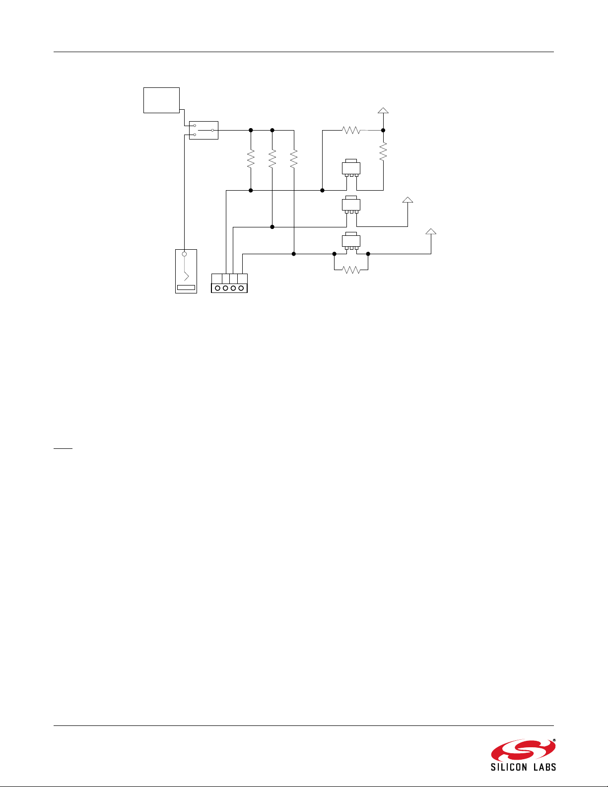
R1, R2, and R4. See the Figure 2 for reference.
J4 provides flexibility for varying the 3 separate supplies
on the board: VRADIO, VAUDIO, and VIO/VMCU.
VRADIO is applied to the VA and VD pins of the
Si4700/01/02/03, VAUDIO powers the audio amplifier
network, and VIO/VMCU powers the baseboard
microcontroller, the reference clock system, and VIO on
the Si4700/01/02/03. Prior to using J4 it is necessary to
remove R1, R2, and R4 as these resistors short the
three connections on J4 together .
When supplying VIO/VMCU via the J4 connector, a
supply > 5 V may be used in conjunction with the 3.3 V
LDO regulator U2. However, U2 may be bypassed by
depopulating U2 and populating R30 with a 0 resistor.
In this case, the VMCU/VIO supply at J4 must lie
between 3.0 and 3.6 V. This condition is necessary t o
ensure reliable operation of the C8051F320.
When supplying VRADIO via the J4 connector, a supply
> 5 V may be used in conjunction with the 3.3 V LDO
regulator U3. However, U3 may be bypassed by
depopulating R14 and populating R25 with a 0
resistor. In such a case, the VRADIO supply at J4 must
lie between 2.7 and 5.5 V. These are the
recommended operating conditions for the
Si4700/01/02/03.
Rev. 0.9 5
Si4700/01/02/03-EVB
R1 R2 R4
U3
U6
VAUDIO
VMCU/VIO
USB
R30
NF
U2
VRADIO
R14
0 ohm
R25
NF
J4
J1
J7
SW1
USB POWER
EXT POWER
GND
VRADIO
VAUDIO
VMCU/VIO
Figure 2. Power Configuration
3.1.4. Expansion I/O connector
The 20-pin Expansion I/O connector J3 provides acce ss
to all the control signals of the Si4700/01/02/03
including the general purpose input/output pins. Pins for
the VA, VD, VIO, and RCLK pins of the Si4700/01/02/03
are also available. All test points on J3 are labeled
indicating the signal available at the pin.
Note: The unlabeled pins on J3 between (a) SCLK and
, and (b) RCLK and GPIO1, provide access to the
RST
system ground.
3.2. Si4700/01/02/03 Daughter Card
3.2.1. Si4700/01/02/03 FM Tuner Chip
The Si4700/01/02/03 (U1) and its bypass capacitors*
are located on the daughter card. The Si4700/01/02/03
is configured to accept a single-ended FM input—the
FMIN pin is grounded and the FMIP pin is connected to
J1 through an ac-coupling capacitor. FMIP is also
connected to the ground wire of the headphone jack
(J3) for easy testing of a headphone wire as the
antenna. Refer to “AN231: Si4700/01 Headphone and
Antenna Interface” for more information.
*Note: We recommend a single bypass capacitor on VD. To
account for various supply designs and layouts, we
recommend that customers make provisions for
bypass capacitors at all supply pins.
3.2.2. Audio Amplifier
The daughter card includes a high-output drive dual opamp chip (U2—daughter card) to buffer the audio
outputs at the LOUT and ROUT pins of the
Si4700/01/02/03. The LOUT and ROUT pins are also
ac-coupled to the inputs of the op-amps on U4 daughter card. To drive the headphone jack, the opamps are connected in a unity-gain, noninverting
configuration and biased at the middle of the audio
power supply . The outp uts of the U2 op-a mps are in turn
ac-coupled to the BNC connectors J10 and J11 on the
baseboard.
The audio amplification network has been designed to
drive resistances of 10 k which is easily achievable on
most audio analyzers. The op-amps have enough drive
capability to drive resistances much lower than 10 k
(e.g. 32 headphones). In such cases, however, the
lower end of the audio spectrum (up to 2.5 kHz) will be
attenuated. This is because the 3-dB points of the highpass filters at the outputs of the op-amps move to higher
frequencies as the output resistance is decreased. Also
note that the op-amps are not protected against
extended short-circuit conditions. Hence, the audio
outputs at J10 and J11 should not be connected to a
mono input if the Si4700/01/02/03 is configured to
produce a stereo output.
6 Rev. 0.9
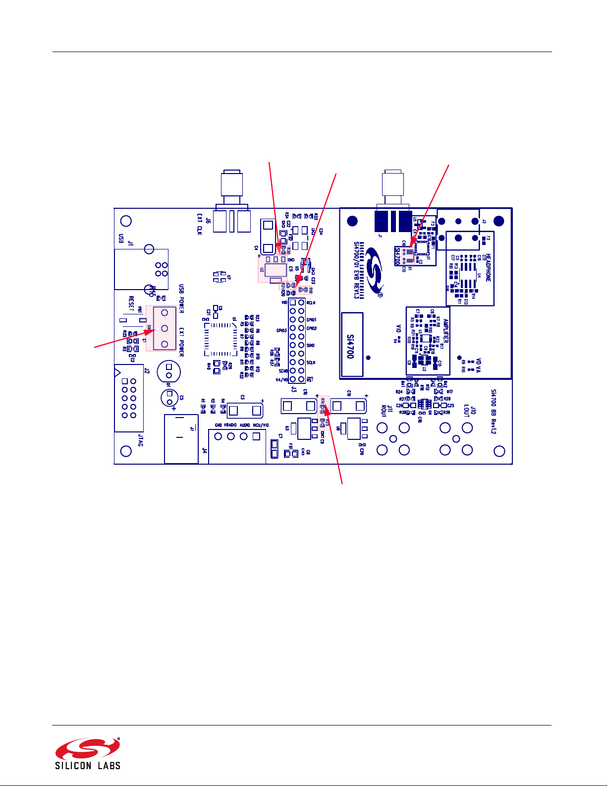
Si4700/01/02/03-EVB
R30, U2
R19, R21
32.768 kHz Crystal Option R2 and R3
on bottom of Daughter Card
SW1
R14, R25
4. EVB Configuration Matrix
Table 1 lists the configuration options the EVB provides, the hardware changes necessary to implement a certain
option, and any associated constraints. Figure 3 shows the locations of the various components required to
configure the EVB.
Figure 3. Locations of Components Used to Configure the EVB
Rev. 0.9 7

Si4700/01/02/03-EVB
Table 1. EVB Configuration Matrix
# Configuration
Variable
1 Reference clock
source
2 Reference clock
source
3 Reference clock
source
4* Power supply
source
5* Power supply
source
6* Power supply
source
7 VIO source Output of U2. None (Default option). 5–26 V input using configura-
8 VIO source Direct from VMCU/VIO
Value of Configuration
Variable
Oscillator on baseboard. None (Default option). None
External clock through J6. Depopulate R19 and popu-
On-chip internal oscillator
utilizing crystal on daughter card.
USB; J1. Position switch, SW1, to
Power brick; J7. Position switch, SW1, to
Bench supply; J4. Depopulate R1, R2, and
terminal of J4.
Hardware Changes Constraints
32.768 kHz, CMOS switch-
late R21 with a 0 resistor.
Depopulate R2 and R3 from
bottom of Si4700/01/02/03
daughter card.
USB POWER.
EXT POWER.
R4.
Depopulate U2 and populate R30 with a 0 resistor.
ing levels at VIO supply level.
GPIO3 is no longer available
and XOSCEN must be
selected when starting the
GUI.
Cannot supply any voltages
via J4.
Cannot supply any voltages
via J4. Power brick must supply 5–26 V.
See Section 3.1.3.
tion option 4, 5, or 6.
3.0–3.6 V input at VMCU/VIO
terminal of J4. Can only be
used in conjunction with configuration option #6.
9 VA/VD source Output of U3. None (Default option). 5–26 V input using configura-
tion option 4, 5, or 6.
10 VA/VD source Direct from VRADIO
terminal of J5.
*Note: For more information, see Section "3.1.3. Power Supply Network" on page 5.
Depopulate R14 and populate R25 with a 0 resistor.
2.7–5.5 V input at VMCU/VIO
terminal of J4. Can only be
used in conjunction with
configuration option #6.
8 Rev. 0.9

Si4700/01/02/03-EVB
PC with USB
Port
RF Generator
Si470x FM Tuner RF
Board
Si470x FM Tuner
Baseboard
USB
Power
Connector
Headphone
Jack
Audio Anaylzer
Rout Lout
CH1
CH2
FMIP
EXT CLK
J4
EVB (as viewed
in Figures 1 & 2)
J1
J1 J3
J11 J10
BNC
Cable
SMA
Cable
J7
Power
Jack
SW1
USB POWER
EXT POWER
5. Hardware Setup
The EVB is connected to a PC, which is running the associated software, as shown in Figure 4.
1. Connect a SMA cable to the SMA connector J1 on the daughter card and apply the desired FM input.
2. Connect one end of a BNC cable to the BNC connector J10 on the baseboard. Connect the other end of
the BNC cable to an audio analyzer, amplifier, or other test equipment with an input impedance >
3. Connect one end of a BNC cable to the BNC connector J11 on the baseboard. Connect the other end of
the BNC cable to an audio analyzer, amplifier, or other test equipment with an input impedance >
4. Make sure SW1 is set for USB POWER.
5. Connect the appropriate end of the USB cable to the USB connector J1 on the baseboard.
6. Connect the other end of the USB cable to a USB port on the PC.
Figure 4. Hardware Setup
10 k.
10 k.
Rev. 0.9 9
Si4700/01/02/03-EVB
6. Getting Started—Software Installation
The Si47xx Windows GUI (graphical user interface) software is designed for use with the Si4700/01/02/03
evaluation board (EVB). The GUI software revision number is available under Help
The GUI software development program uses a host machine USB port to communicate with the Si47xx EVB and
is tested for use with Windows XP and Windows 2000.
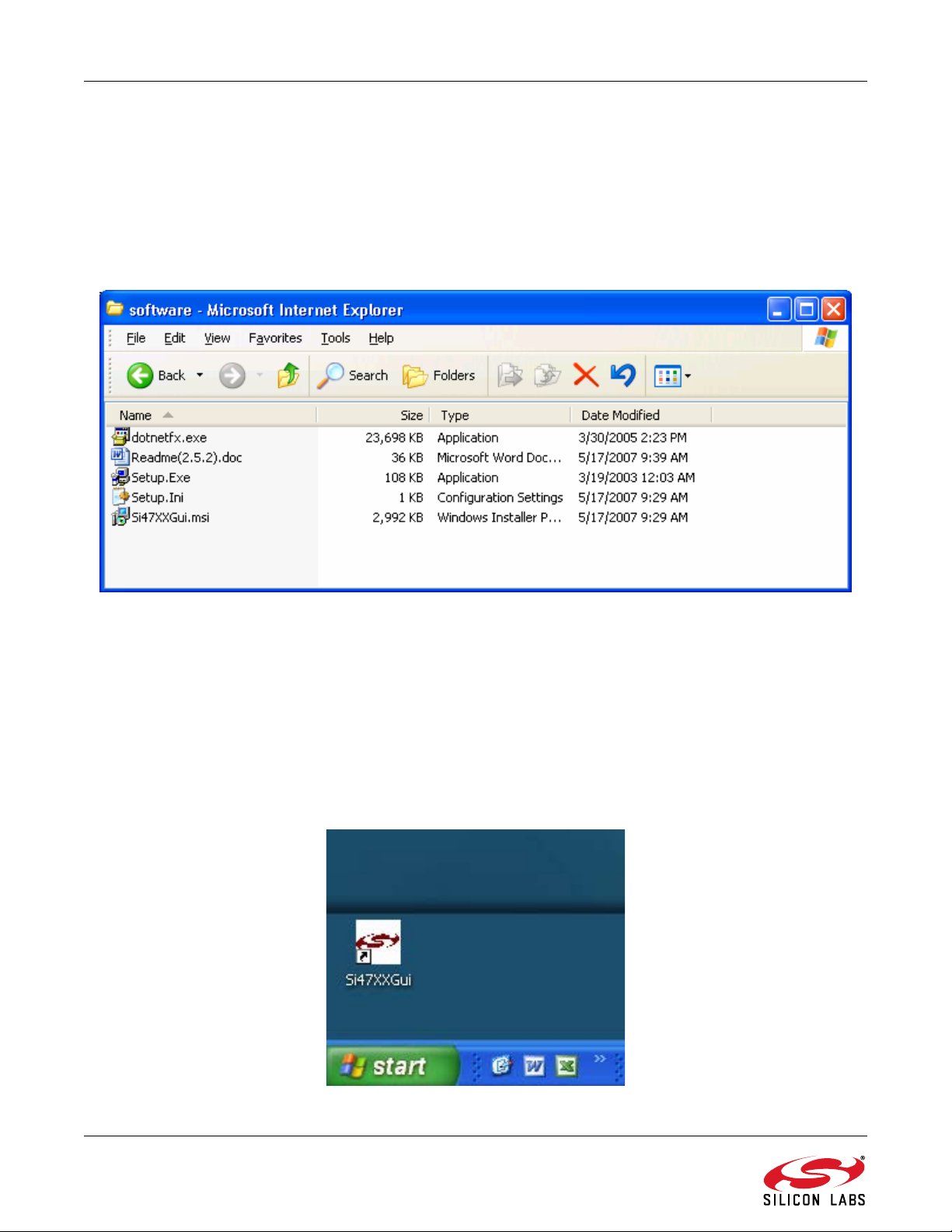
To install, insert the Silicon Laboratories Si47xx CD into the host machine CD drive and launch Windows Explorer.
Open the CD to explore the contents in a window like the one shown in Figure 5 below.
About.
Figure 5. Installation and Setup Start Screen
Important: Open and read the Readme.doc file at this point. It may contain information that is not captured here,
and which could be very important to the functionality of the EVB or software.
Run the Setup.Exe and follow the instructions on the screen.
Note: If you get this error message: "This setup requires the .NET F ramework version 4.0," then you should in stall the .NET
Framework that is provided on the CD and re-run the setup. The GUI requires version 4.0; however, multiple versions
such as 2.0, 3.0, and 5.0 can be installed simultaneously.
After installation is finished, an Si47XXGUI icon will appear on your desktop. Launch the software by clicking this
icon on the desktop as shown in Figure 6.
Figure 6. Launching the GUI
10 Rev. 0.9
Si4700/01/02/03-EVB
6.1. Connecting to the EVB
6.1.1. Initialization
The first window will show the following connect window. This window can be accessed anytime from the top menu
by selecting File
Initialize.
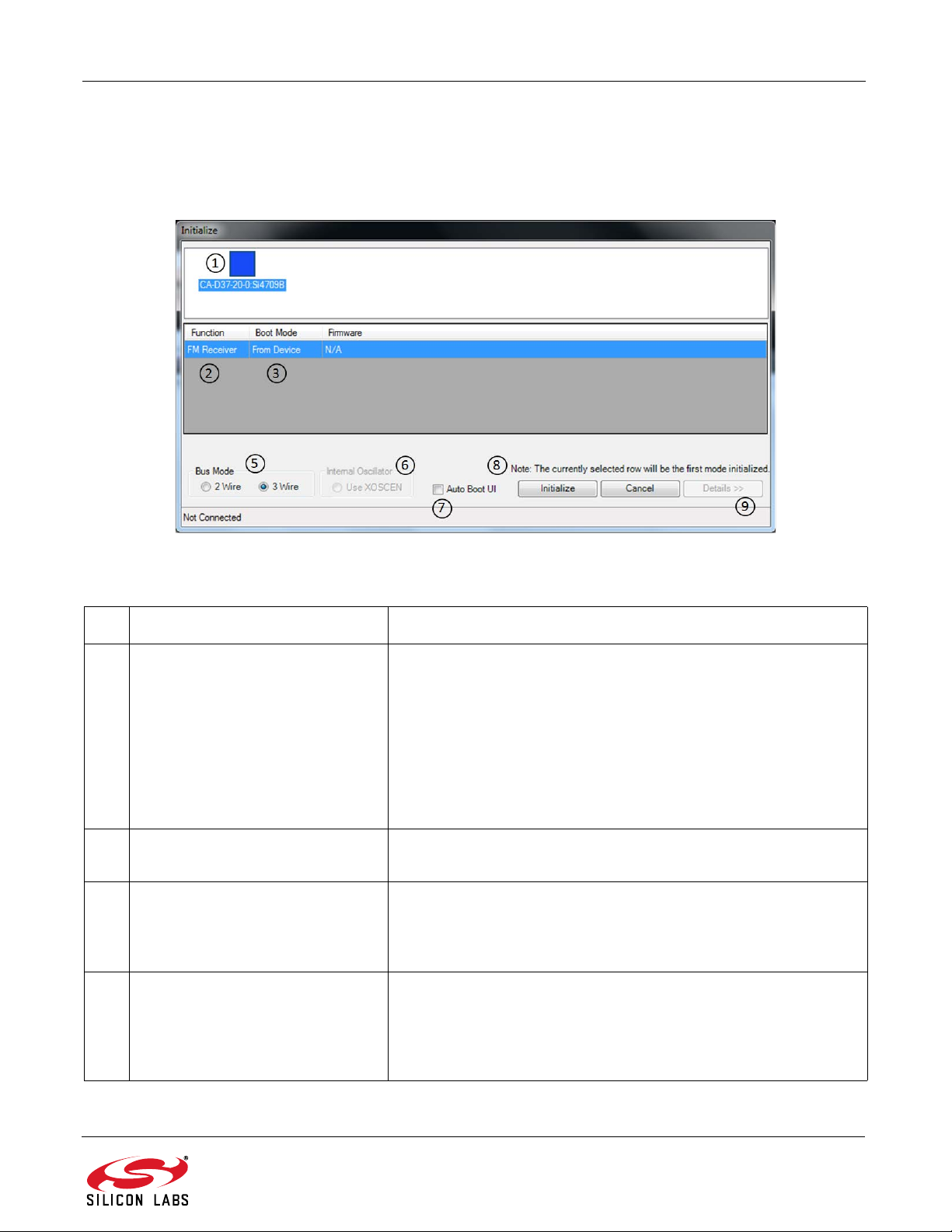
Figure 7. Initialization Screen
Table 2. Initialization Screen Explanations
# Name Explanation(s)
1 Connected Board List Box If there are one or more EVBs detected, each board will be dis-
played with its corresponding part number and serial number. If
there are no EVBs connected this list box will be empty.
If your board is connected but the serial number is not displayed,
Disconnect and reconnect the EVB or press the reset button on
the EVB. If the drop down box is grayed out, then the software is
currently connected to the board with the serial number that is displayed. To disconnect from this board, select “Cancel” and then
File→Disconnect.
2 Function For the Si4700/01/02/03 boards, this drop down selection will only
allow “FM Receiver.”
3 Boot Mode
4 Reset This option is only available if the board was previously initialized
Load Firmware from Device—will boot the chip using the
firmware from NVRAM in the device.
Initialize Only—will perform an open and reset but will not boot
the chip.
with the “Initialize Only” option. When selected, the Si470x is reset
before performing the selected action. By not selecti ng this optio n,
it is possible to make changes to the r egister map prior to enabling
the device.
Rev. 0.9 11

Si4700/01/02/03-EVB
Table 2. Initialization Screen Explanations (Continued)
# Name Explanation(s)
5 Bus Mode Selects the communication mode used to communicate with the
part in either 2-Wire or 3-Wire mode.
6 Internal Oscillator If checked then the Daughter card crystal and on-chip oscillator
will be used to clock the Si4700/01/02/03. If the default is
unchecked, use the baseboard oscillator. Refer to Table 1, “EVB
Configuration Matrix,” on page 8 for important oscillator information. Note that the on-chip oscillator is only available on revision B
silicon or later.
7 Auto Boot If checked, the next time the GUI starts and only one EVB is
connected, the initialize screen will not appear and the part will be
booted automatically using the previous settings. This may be
changed by selecting File
8 Initialize/Cancel Buttons Press Initialize to activate the chip with the selected options
Press Cancel to exit.
9 Details Button Not available with Si4700/01/02/03 parts.
Initialize and unchecking the box.
6.1.2. Board Discovery Bus Mode
The initialize process can be configured to use either 2-wire or 3-wire bus mode. This can be configured by
selecting File
This feature is useful when using the Silabs EVB and GUI to control a prototype that is designed to use one bus
mode only.
Board Discovery Bus Mode.
12 Rev. 0.9
6.2. Running the Software
1
2
3
4
5
6
7
8
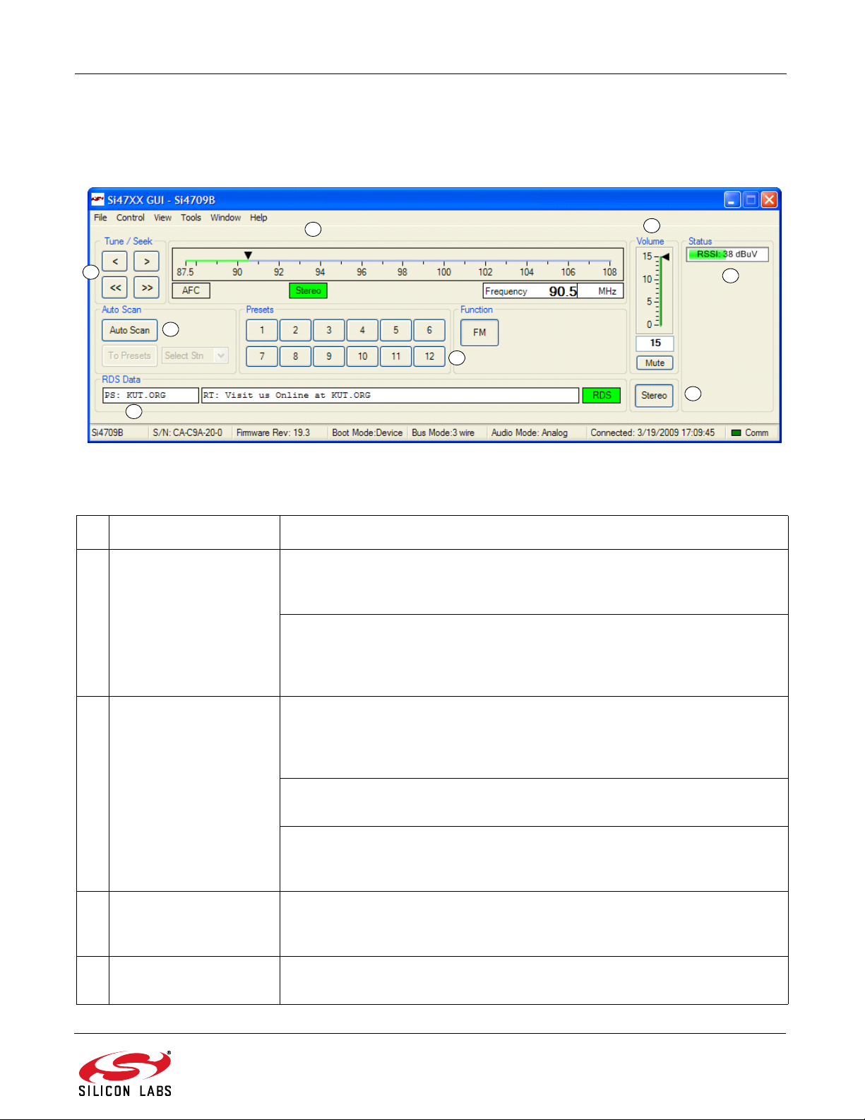
6.2.1. FM Receiver Main Window
The FM receiver main window will appear after initialization.
Figure 8. FM Receiver Main Window
Si4700/01/02/03-EVB
Table 3. FM Receiver Main Window Descriptions
# Name Explanation(s)
1 Tune/Seek Tune Down (<), Tune Up (>) buttons execute a single channel step according
to the channel spacing setting. The channel spacing setting can be set in the
property window.
Seek Down (<<), Seek Up (>>) buttons execute a seek up or down to the next
received FM signal meeting or exceeding the seek settings within the selected
band. The seek setting Received Signal Strength Indicator (RSSI) threshold
can be set in the property window.
2 Frequency Slider Bar,
Mono/Stereo, AFC Rail
3 Volume, Mute Select the Si4700 output volume (0-15) by moving the slider bar pointer. Press
4 Auto Scan, To Presets,
Select Stn
The Frequency Display indicates the frequency in MHz. To change the
Frequency, drag the pointer in the Frequency Slider Bar to the desired
frequency. The frequency may also be changed by changing the value in the
display.
AFC Rail indicator will be red if the tuned frequency is in an AFC rail state,
otherwise the indicator will be grey.
The Stereo / Mono Indicator is a tri-state indicator displaying “Stereo” (green),
“Mono” (grey), or forced “Mono” (Yellow). The Stereo / Force Mono state can
be selected by (7).
the Mute button to mute the radio. If the radio is muted, the button will be red.
Press the Mute button again to remove the muting.
The Auto Scan button will find all the stations that meet the seek threshold
settings in the property window.
Rev. 0.9 13

Si4700/01/02/03-EVB
Table 3. FM Receiver Main Window Descriptions (Continued)
# Name Explanation(s)
5 Presets Press the desired button to tune to the frequency displayed on the button. To
store a new value to the preset button, tune to the desired freq uency and then
press and hold the desired button for 1.5 seconds. The button will then change
to indicate the stored frequency.
6 RSSI The RSSI displays the received signal strength of the signal in dBμV.
7 Mono/Stereo Select
Button
8 RDS Data
(PT/RT/RDS Indicator)
By default, the receiver is configured for stereo mode. To force mono, click the
button. To return to stereo mode, click the button again.
Provides a summary of the current RDS data if available. PS contains the
Program Service text, RT cont ains the Radio Text, and the RDS indicator turns
green when RDS data has been synchronized. For more RDS data select
Window
RDS Receive Data.
14 Rev. 0.9

Si4700/01/02/03-EVB
1
2
3
4
6
5
6.2.2. FM Receiver RDS Window
The FM Receive RDS window allows the user to view program service, program type, PI code, radio text, clock,
group error rate, sync and display times, an alternate frequency list, and group statistics. Select Window
Receive Data.
RDS
Figure 9. FM Receiver Settings RDS Window
Table 4. FM Receiver Settings RDS Window Descriptions
# Name Explanation(s)
1 Radio Data Service PS: Program Service Indicator (8 characters).
RT: Radio Text Indicator (64 characters).
CT: Clock Indicator showing time, day, and date
PTY: Program Type Indicator
PI: PI Code Indicator
2 Sync Times Time required to synchronize, display radio text, and display
program service.
3 RDS Synchronization Indicator Indicates that RDS is synchronized.
4 Alternate Frequency Indicator When present, shows a list of alternate frequencies.
5 Group Counters Provides the total number and percentage breakdown of group
types 0–15, A / B. To view this information, select Window
Group Counters. Please refer to Figure 54.
6 Block Counters Provides the block error rates after tune and after RDS sync.
RDS
Rev. 0.9 15

Si4700/01/02/03-EVB
Table 4. FM Receiver Settings RDS Window Descriptions (Continued)
# Name Explanation(s)
After Tune Error Rate: After tune (STC interrupt), the ideal num-
ber of blocks the FM tuner should have received is calculated.
Also, the number of accepted blocks and errors are calculated.
For Si4700/01/02/03 parts, the ideal numb er is not available in the
UI.
Error Rate = number of errors / number of ideal blocks after tune.
16 Rev. 0.9

Si4700/01/02/03-EVB
1
2
3
4
6.2.3. RDS Group Counters
This screen allows you to view the RDS Group Data in detail. This screen is accessed from the RDS Group
Counters option in the Window menu.
Figure 10. RDS Group Counters Window
Table 5. RDS Group Counters Window Explanations
# Name Explanation(s)
1 Histogram A histogram of all the RDS Group counters displayed for the
tuned station.
The RDS statistics begin accumulating once a new station has
been tuned.
2 RDS Group Labels RDS group labels (e.g., 0A, 0B, 1A, etc.) If there has been RDS
data for that particular group (e.g., 2A), then the label will be
displayed in Bold type. If there has not been RDS data for the
group, then the label will be in light type indicating no data for that
group.
3 Tooltips By moving your mouse over a group label, the number of count s /
total count and percentage and group designation will be
displayed.
4 Cancel Press Cancel to close the window.
Rev. 0.9 17

Si4700/01/02/03-EVB
6.2.4. RSSI Graph Screen
The RSSI Graph Window allows the user to plot RSSI across the FM band. Bitmap data can be saved to file by
selecting File
window can be accessed by selecting Window
Save as Bitmap and tabulated data can be saved to file by selecting FileSave to .csv. This
RSSI Graph.
Figure 11. FM Receiver RSSI Graph Window
Table 6. FM Receiver RSSI Graph Window Descriptions
# Name Explanation(s)
1 RSSI Graph Indicates RSSI graph will be drawn.
2 Line / Bar Select between drawing in bar mode (depicted as green) or in
continuous line mode (depicted as yellow).
3 Draw Click this to start plotting the graph.
4 Seek Threshold (RSSI) Draw the RSSI seek threshold as specified in the properties. The
RSSI seek threshold is shown in red.
5 Delete Plots Select the desired plot to delete in the drop down control and then
click Clear to delete that plot.
18 Rev. 0.9

Si4700/01/02/03-EVB
1
2
3
4
6.2.5. Register Map Display
This screen displays the settings of the register map as detailed in the Si4700/01 or Si4702/03 data sheets. This
display is accessed by selecting Window
Register Map.
Figure 12. Register Map Window
Table 7. Register Map Window Explanations
# Name Explanation(s)
1 Multiple-bit Fields Multiple-bit fields can be changed by clicking the up or down
2 Single-bit Fields Single-bit fields can be changed between 1 and 0 by clicking the
3 Communication LED The register map is updated whenever the Updating LED is green.
4 Tooltips Moving the cursor over the register number will give the register
arrows or by typing the value directly. The setting will be written to
the chip when the value is changed.
radio button on and off, respectively. The setting will be written to
the chip when the value is changed.
The update time is selectable from the View
menu. Updates may be disabled by checking or unchecking
Control
name as a tooltip. Moving over each numeric field label will give the
bit range as a tooltip.
Update.
Rev. 0.9 19
Session Preferences

Si4700/01/02/03-EVB
6.2.6. Log Band Scan
Selecting Tools
data, RDS acquisition times, and the contents of each register. The scan feature starts with the first frequency in
the band (CHAN = 0) and then seeks to the first station that meets the seek criteria (SEEKTH, SKCNT, SKSNR).
When a valid station is found, the software waits at the station for the time specified by View
Preferences
software logs the register settings and seeks to the next valid station. If RDS is available, the software waits an
additional delay as specified by View
expires, the software logs the RDS information and register settings and seeks to the next valid station. While
scanning, the software displays a green "Scanning" notice below the menu bar. The scan can be aborted by
selecting the Tools
comma separated format and is available for analysis in a text editor or spreadsheet.
6.2.7. Log Raw RDS Data
Selecting Tools
separated format. The software then logs all raw RDS data that is received, the station it is received on, and the
time at which it was received. The logging will continue until Tools
at which point the file is saved and available for analysis in a text editor or spreadsheet.
6.2.8. Log Channel Info
Selecting Tools
separated format. The software then logs all register values and the time at which it was received. The logging will
continue until Tools
analysis in a text editor or spreadsheet.
6.2.9. Log Device Commands
Selecting Tools
timestamp data will be logged as text. The logging will continue until Tools
second time, at which point the file is saved and available for analysis in a text editor.
6.2.10. Startup Preferences Dialog
The startup Preferences Dialog is accessed via the top menu View
customize standard settings for your local needs. All startup preferences are saved in the user.ini file.
Log Band Scan allows you to specify a filename and begin a scan of the entire band for RDS
Session
Scan Log After Tune Delay (sec) and then checks if RDS is available. If RDS is not available, the
Session PreferencesScan Log RDS Log Delay (sec). When this delay
Log Band Scan a second time. When the scan completes, the filename given is saved in
Log Raw RDS Data prompts for a filename in which all RDS data will be logged in comma
Log Raw RDS Data is selected a second time
Log Channel Info prompts for a filename in which all register values will be logged in comma
Log Channel Info is selected a second time, at which point the file is saved and available for
Log Device Commands prompts for a filename in which all software API calls and data with
Log Device Commands is selected a
Startup Preferences. It enables you to
20 Rev. 0.9

Si4700/01/02/03-EVB
2
1
Figure 13. Startup Preferences
Table 8.
# Name Explanation
1 Default Radio Settings Select the Radio Parameters that you want loaded each time you start the
application. Refer to Table 10, “GUI Properties,” on page 24 for an explanation of
each property.
2 OK/Cancel Press OK to save the values, press Cancel to exit without saving. This data is
stored in the file User.ini in your application directory.
Startup Preferences Explanations
Rev. 0.9 21

Si4700/01/02/03-EVB
1
2
3
4
5
6
7
8
6.2.11. Session Preferences Dialog
The session Preferences Dialog is accessed via the top menu View
adjust settings that will take effect immediately. The settings will also be used the next time you start the
application. All session preferences are saved in the user.ini file.
Session Preferences. It enables you to
Figure 14. Session Preferences
Table 9. Session Preferences Explanations
# Name Explanation(s)
1 Radio Panel Update Rate Select the update rate for the radio panel tab. The default is 0.5 seconds.
2 Reg Map Update Rate Select the update rate for the register map tab and property grid. This value
must be greater than the GUI Update rate or you will get an error.
3 RDS Error Checking Select the default method for RDS error checking performed on the baseboard.
For more description, see RDS Error Checking in Table 10.
4 RDS Text Decode Select the default character set for displaying RDS data.
5 Scan Log After Tune
Delay
6 Scan Log RDS Log Delay Select how many seconds are allowed during a Tools
22 Rev. 0.9
Select how many seconds the Tools
determine if the found channel has RDS. If the channel has RDS, then the
RDS Log Delay applies, otherwise it seeks to the next channel.
gather RDS data, RT time, and PS time. This timer begins when the “After
Tune Delay” expires.
Log Band Scan feature waits to
Log Band Scan to

Si4700/01/02/03-EVB
Table 9. Session Preferences Explanations (Continued)
# Name Explanation(s)
7 Leave Radio On Upon Exit Check this box if you want to leave the radio playing when you exit the
application, otherwise it will turn off.
8 OK/Cancel Press OK to save the changes, cancel to exit without saving.
6.2.12. Help About Screen
This screen displays important information regarding version information of the application, EVB, and chip
firmware.
Figure 15. Help About Screen
Rev. 0.9 23

Si4700/01/02/03-EVB
Table 10. GUI Properties
Property Description Settings
Frequently Used
BAND Select the band of frequencies US/Europe, 0 = 87.5 = 108 MHz
Japan Wide, 1 = 76–108 MHz
Japan Normal 2 = 76–90 MHz
MONO Mono Select 0 = Stereo
1=Force Mono
PTYDECODE RDS Type 0 = RDS decoding
1 = RBDS decoding
SEEKTH Select the RSSI threshold to use
when seeking manually or automati-
cally.
SKCNT Seek Impulse Noise Count 0–7 (See da ta sheet)
SKSNR Seek Signal to Noise Ratio 0–15 (See data sheet)
SP ACE Select the spacing between tunable
frequencies.
Seek/Tune
0–70
RSSI value in dBµV
0=200kHz (US),
1 = 100 kHz (Europe/Japan)
2=50kHz,
AFCRL AFC Rail 0 = AFC Not Railed
1 = AFC Railed
CHAN Channel Select See data sheet
READCHAN Read Channel See data sheet
SEEK Seek Enable 0 = Disable
1 = Enable
SEEKTH Select the RSSI threshold to use
when seeking manually or automatically.
SEEKUP Seek Direction 0 = Seek Down
SF/BL Seek Fail/Band Limit 0 = Seek Successful
SKCNT Seek Impulse Noise Count 0–15 (See data sheet)
SKMODE Seek Mode 0 = Wrap at band Limits
SKSNR Seek Signal to Noise Ratio 0–7 (See data sheet)
ST Stereo Indicator 0 = Mono
STC Seek/Tune Complete - Set when the
seek or tune operation completes.
0–70
RSSI value in dBµV
1 = Seek Up
1 = Seek Fail / Band Limit Reached
1 = Stop at band limits
1 = Stereo
0 = Complete
1 = Not Complete
24 Rev. 0.9

Si4700/01/02/03-EVB
Table 10. GUI Properties (Continued)
Property Description Settings
STCIEN Seek/Tune Complete Interrupt
Enable - when this feature is
enabled, all activity on the SDIO pin
is stopped during seek and tune so
there is no update of the seek progress.
TUNE Tune 0 = Disable
Audio Control
BLNDADJ Stereo/Mono Blend Level Adjust-
ment
DE De-emphasis 0 = 75 uS
DMUTE Mute 0 = Mute Disable
DSMUTE Softmute 0 = Softmute Enable
SMUTEA Softmute Attenuation 00 = 16 dB
SMUTER Softmute Rate 00 = fastest
VOLEXT Volume Extend 0 = Volume table dynamic range is
VOLUME Volume 0(mute)–15(max)
Misc Status
0 = Disable Interrupt
1 = Enable Interrupt
1 = Enable
00 = 31–49 dBµV
01 = 37–55 dBµV
10 = 19–37 dBµV
11 = 25–43 dBµV
1=50uS
1 = Mute Enable
1 = Softmute Disable
01 = 14 dB
10 = 12 dB
11 = 10 dB
01 = fast
10 = slow
11 = slowest
28 dBFs.
1 = Expands volume table dynamic
range to 58 dBFs. See AN281 for more
details.
DEV Device ID Read only
FIRMWARE Firmware Version Read only
MFGID Manufacturer ID (hex) Read only 0x242
PN Chip Part Number 1 = Si4700/01/02/03 (Read only)
REV Chip Hardware Revision Read only
Misc Control
AGCD Automatic Gain Control 0 = AGC Enable
1 = AGC Disable
AHIZEN Analog Output Hi-Z Enable 0 = Hi-Z Disable
1 = Hi-Z Enable
Rev. 0.9 25

Si4700/01/02/03-EVB
Table 10. GUI Properties (Continued)
Property Description Settings
DISABLE Powerup Disable 0 = Not active
1 = Initiate Powerdown
ENABLE Powerup Enable 0 = Not active
1 = Initiate Powerup
GPIO1 General Purpose I/O 1 General Purpose I/O 1 00 = High Impedance
01 = Reserved
10 = Low
11 = High
GPIO2 General Purpose I/O 2 General Purpose I/O 2 00 = High Impedance
01 = STC/RDS Interrupt
10 = Low
11 = High
GPIO3 General Purpose I/O 3 General Purpose I/O 3 00 = High Impedance
01 = Mono/Stereo Indicator
10 = Low
11 = High
XOSCEN Crystal Oscillator Enable - this set-
ting must be selected on the Initialize screen.
RDS Status
BLERA RDS Block A Error Count 00 = 0 errors
BLERB RDS Block B Error Count 00 = 0 errors
BLERC RDS Block C Error Count 00 = 0 errors
BLERD RDS Block D Error Count 00 = 0 errors
RDSR RDS Ready 0 = No RDS Ready
RDSS RDS Synchronized 0 = RDS not synchronized
RDS Control
RDS RDS Enable 0 = Disable
0 = External Clock
1 = On-chip Oscillator
01 = 1–2 errors
10 = 3–5 errors
11 = 6+ errors
01 = 1–2 errors
10 = 3–5 errors
11 = 6+ errors
01 = 1–2 errors
10 = 3–5 errors
11 = 6+ errors
01 = 1–2 errors
10 = 3–5 errors
11 = 6+ errors
1 = New RDS Ready
1 = RDS synchronized
1 = Enable
26 Rev. 0.9

Si4700/01/02/03-EVB
Table 10. GUI Properties (Continued)
Property Description Settings
RDS ERROR CHECKING RDS Error Checking Three options are available:
Minimum - displays the RDS
data exactly as it is received
from the Si4701/03.
Mid-level - RDS data is verified
by comparing the current byte
with the previous bytes received
from the Si4701/03. Only
consistent data is displayed. If
the A/B flag toggles, the data is
displayed regardless of
verification status. Data is more
error free than the minimum
setting, but some errors may be
displayed on stations using the
A/B flag improperly.
Maximum - RDS data is verified
as in the mid-level setting, but
the A/B flag is ignored. Data is
virtually error free, but may take
longer to display.
RDS Text Decoding RDS Text Decoding Mode ASCII
Big 5 (Traditional Chinese)
Default (Use system code page)
UTF-8
Unicode
RDSIEN RDS Interrupt Enable 0 = Disable interrupt
1 = Enable interrupt
RDSM RDS Verbose Mode 0 = Standard
1=Verbose
EVB MCU
Headphone Amp Turns on and off the headphone
amplifier
Rev. 0.9 27
0=Off
1=On

Si4700/01/02/03-EVB
7. Schematics
28 Rev. 0.9
Figure 16. Si4700 Baseboard

Si4700/01/02/03-EVB
Figure 17. Si4700/01 Daughter Card
Rev. 0.9 29

Si4700/01/02/03-EVB
30 Rev. 0.9
Figure 18. Si4702/03 Daughter Card

8. Layout
8.1. Baseboard
Si4700/01/02/03-EVB
Figure 19. Baseboard—Primary Assembly Silkscreen
Figure 20. Baseboard—Primary Side
Rev. 0.9 31

Si4700/01/02/03-EVB
Figure 21. Baseboard—Ground Plane
Figure 22. Baseboard—Power Plane
32 Rev. 0.9

Si4700/01/02/03-EVB
Figure 23. Baseboard—Secondary Side
Rev. 0.9 33

Si4700/01/02/03-EVB
8.2. Si4700/01 Daughter Card
Figure 24. Si4700/01 Daughter Card—Primary Assembly Silkscreen
Figure 25. Si4700/01 Daughter Card—Primary Side
34 Rev. 0.9

Si4700/01/02/03-EVB
Figure 26. Si4700/01 Daughter Card—Ground Plane
Figure 27. Si4700/01 Daughter Card—Power Plane
Rev. 0.9 35

Si4700/01/02/03-EVB
Figure 28. Si4700/01 Daughter Card—Secondary Assembly Silkscreen
Figure 29. Si4700/01 Daughter Card—Secondary Side
36 Rev. 0.9

8.3. Si4702/03 Daughter Card
Si4700/01/02/03-EVB
Figure 30. Si4702/03 Daughter Card—Primary Assembly Silkscreen
Figure 31. Si4702/03 Daughter Card—Primary Side
Rev. 0.9 37

Si4700/01/02/03-EVB
Figure 32. Si4702/03 Daughter Card—Ground Plane
Figure 33. Si4702/03 Daughter Card—Power Plane
38 Rev. 0.9

Si4700/01/02/03-EVB
Figure 34. Si4702/03 Daughter Card—Secondary Assembly Silkscreen
Figure 35. Si4702/03 Daughter Card—Secondary Side
Rev. 0.9 39

Si4700/01/02/03-EVB
9. Bill of Materials
9.1. Bill of Materials—Baseboard
Table 11. Bill of Materials—Baseboard
ITEM QTY REFDES DESCRIPTION VALUE FOOTPRINT MFG/Vendor Part number
1 1 C1. CAP,SM,0603,1UF,X7R 1 UF RC0603 VENKEL C0603X7R100-105KNE
2 3 C10,C19,C4 CAP,SM,7343,15UF,10% 15UF 7343_EIAD VISHAY PCT15/20DK
3 9 C11,C2,C20,C21,C22,
4 1 C18 CAP,SM,0402,0.1UF,10% NF CC0402 VENKEL C0402X7R160-104KNE
5 2 C25,C26 CAP,SM,0805 NF C0805 VENKEL C0805X7R100-225KNE
7 1 C5 CAP,TANT,RADIAL 4.7UF KEMET TB4.7/16K1
8 1 C6 CAP,0.1UF,X7R,0805,50V,5% 0.1UF C0805 Venkel NMC0805X7R104K50TRP
9 1 C7 CAP,SM,3216 10UF 3216_EIAA VISHAY PCT10/16AK
10 1 D1 LED, T-1 3/4 RED DIFFUSED LITEON LTL-10223W
11 2 FB1,FB2 FERRITE BEAD,SM RC0805 Steward MI0805K400R-00
12 1 J1 CONN,TH,USB,RCPT,TYPE B CONN-USB-B Kycon KUSB-BS-1-N-BLK
13 2 J10,J11 CONN,BNC,TH,RIGHT ANGLE,COAX-
14 1 J2 HEADER,SHROUDED,5X2 CONN2X5_SHRO
15 1 J3 CONN,TH,2X10,HDR CONN2X10 SAMTEC TSW-110-07-G-D
16 1 J4 PCB TERMINAL BLOCK, 4 POSITION PHOENIX CON-
17 1 J5 CONN,TH,TFM,HDR,2X20,0.05X0.05IN
18 1 J6 CONN, SMA, EDGEMOUNT SMA-EDGE-5 Y-Connect RA2EJ26G
19 1 PB1 BUTTON,SM,LIGHT-
20 15 R1,R2,R4,R10,R12,
21 1 R11 RES,SM,0402,1% 22.1 RC0402 VENKEL CR0402-16W-22R1FT
22 4 R13,R17,R18,R24 RES,SM,0402,160,5% NF RC0402 Venkel CR0402-16W-164JT
23 1 R19 RES,SM,0402,1% 33 RC0402 VENKEL MCR01MZPF33R0
24 2 R20,R21 RES,SM,0402 NF RC0402 ?
26 5 R25,R26,R30,R33,R34 RES,SM,0402 NF RC0402
27 1 R3 RES,SM,0603 1K RC0603 VENKEL CR0603-10W-1001FT
28 1 R35 RES,SM,0402 1K RC0402 VENKEL CR0402-16W-102J
29 2 R36,R37 RES,SM,0402 2K RC0402 VENKEL CR0402-16W-202JT
30 1 R40 RES,SM,0805 470 RC0805 VENKEL CR0805-8W-471JT
31 2 R41,R42 RES,SM,0603 0R RC0603 VENKEL CR0603-10W-000T
32 1 U1 IC,SM,C8051F320,MCU,LQFP-
33 3 U2,U3,U6 VOLTAGE_REG,3_3 V,500MA,SOT223 SOT223 NATIONAL SEMI-
34 1 U4 NF SOT23-8N MAXIM
35 1 U5 IC,SINGLE SCHNITT TRIGGER BUFFER SOT23-5 TI SN74LVC1G17DBVR
C23,C24,C8,C9
R14,R15,R23,R27,R28,
R29,R32,R38,R39,R5,
R6,R7,R8,R9
CAP,SM,0402,0.1UF,10% 0.1 UF CC0402 VENKEL C0402X7R160-104KNE
IAL,NICKEL-PLATED
PITCH
TOUCH,160GF,6X3.5MM
RES,SM,0402 0R RC0402 VENKEL CR0402-16W-000T
LQFP-32-LDSILICON LABO-
32,9X9MM
CONN-BNC_RT AMP 413631-3
UDED
CONN40-TFM-
T/H
EVQPPBA25 PANASONIC EVQ-PPBA25
RATORIES
3M 2510-6002UB
TACT
SAMTEC TFM-120-01-S-D
'C8051F320/1
CONDUCTOR
1803293
LM2937IMP-3.3
40 Rev. 0.9

Si4700/01/02/03-EVB
Table 11. Bill of Materials—Baseboard (Continued)
ITEM QTY REFDES DESCRIPTION VALUE FOOTPRINT MFG/Vendor Part number
36 1 U7 SOT143 LITTLEF USE SP0503BAHT
37 1 X1 32_768KHZ,OSC,SM OSCILLATOR ECS ECS-327SMO-TR
38 1 01 Shield,SM LeaderTech 20S-CBSF-0.75X1.0X0.2
39 4 02 Nylon Stand-offs Eagle Plastic
40 4 03 Nylon Screws Eagle Plastic
41 1 05 Pluggable Terminal Header PHOENIX CON-
42 2 06 Nylon Stand-offs Eagle Plastic
43 2 7 Nylon Screws Eagle Plastic
44 1 SW1 2 throw 3 pole switch 3pin_switch E-switch 500ssp1s1m2rea
45 1 J7 2.1 mm power connector PJ-002A CUI PJ-002A
Devices
Devices
TACT
Devices
Devices
9.2. Bill of Materials—Si4700/01 Daughter Card
Table 12. Bill of Materials—Si4700/01 Daughter Card
TSP3
P440.375
1803594
13SP040
P440.75
ITEM QTY Side REFDES DESCRIPTION VALUE FOOTPRINT MFG/Vendor MFG/Vendor_PN
1 1 Top C2 CAP,SM,0402,X7R 22NF CC0402 MURATA GRM155R71E223KA61D
1 1 Bottom C1 CAP,SM,0402,X7R 22NF CC0402 MURATA GRM155R71E223KA61D
2 2 Top C10,C9 CAP,SM,0805 2.2UF C0805 VENKEL C0805X7R100-225KNE
3 1 Top C11 CAP,SM,0402,X7R 10NF CC0402 MURATA GRM155R71E103KA01D
4 2 Top C8,C12 CAP,SM,0402,X7R 0.1UF CC0402 MURATA GRM155R71C104KA88D
4 1 Bottom C3 CAP,SM,0402,X7R 0.1UF CC0402 MURATA GRM155R71C104KA88D
5 2 Top C13,C14 CAP,SM,0603,0.33UF,X7R 0.33UF RC0603 VENKEL C0603X7R160-334KNE
6 5 Top C4,C5,C17,C18
7 2 Top C15,C16 CAP,SM,0402 22PF CC0402 VENKEL C0402C0G500-220JNE
9 2 Top C6,C7 CAP,SM,0603,1UF,X7R 1UF RC0603 VENKEL C0603X7R100-105KNE
10 1 Top J1 SMA,EDGE-MOUNT,GOLD PLATED SMA-EDGE-5 YAZAKI RA2EJ2-6G
11 1 Top J2 CONN,SM,2X20,SFM CONN-2X20-SFM SAMTEC SFM-120-02-S-D-A
12 1 Top J3 CONN,AUDIO JACK,3.5MM,STEREO SJ3543N DIGIKEY CP-3543N-ND
13 3 Top F1,F2,F3 Ferrite Bead,SM,0603 2500ohm FB0603 MURATA BLM18BD252SN1D
14 1 Top L1 Ind,0603,SM 270nH IND0603 MURATA LQW18ANR27J00D
16 3 Top R10,R4,R9 RES,SM,0402 0R RC0402 VENKEL CR0402-16W-000T
17 2 Bottom R2,R3 RES,SM,0402 0R RC0402 VENKEL CR0402-16W-000T
18 4 Top R11,R12,R13,R
19 2 Top R14,R15 RES,SM,0603 10K RC0603 VENKEL CR0603-16W-103JT
20 8 Top R17,R18,R19,R
21 1 Top U1 IC,SM,SI4700,MLP24 MLP24-4MM SILICON LABORA-
,C19
16
20,R5,R6,R7,R
8
CAP,SM,0402,X7R 100PF CC0402 MURATA GRM1555C1H101JZ01D
RES,SM,0603 20K RC0603 VENKEL CR0603-16W-203JB
RES,SM,0402,160K,5% 160K RC0402 VENKEL CR0402-16W-164JT
TORIES
SI4700
Rev. 0.9 41

Si4700/01/02/03-EVB
Table 12. Bill of Materials—Si4700/01 Daughter Card (Continued)
ITEM QTY Side REFDES DESCRIPTION VALUE FOOTPRINT MFG/Vendor MFG/Vendor_PN
22 1 Top U2 IC,SM,AUDIO AMP,SOT23-8 SOT23-8N MAXIM MAX4232AKA+T
23 1 Top U3 IC,SM,UHS DUAL SPS T,8 LEAD US8 US8 FAIRCHILD SEMI-
24 1 Top U4 IC,SM,HEADPHONE AMP M08A NATIONAL SEMI-
25 1 Top U5 IC,SM,ESD PROTECTION
26 1 Top X1 OSC,SM,Crystal 32.768KHz,Chip 32.768KH
DIODE,SOT23-3
z
SOT23-3N CALIFORNIA
CONDUCTOR
CONDUCTOR
MICRO DEVICES
Epson FC-135
9.3. Bill of Materials—Si4702/03 Daughter Card
Table 13. Bill of Materials—Si4702/03 Daughter Card
ITEM QTY REFDES DESCRIPTION VALUE FOOTPRINT MFG/Vendor MFG/Vendor_PN
1 2 C1,C2 CAP,SM,0402,X7R 22 NF CC0402 MURATA GRM155R71E223KA61D
2 2 C10,C9 CAP,SM,0805 2.2 UF C0805 VENKEL C0805X7R100-225KNE
3 1 C11 CAP,SM,0402,X7R 10 NF CC0402 MURATA GRM155R71E103KA01D
4 3 C8,C12,C3 CAP,SM,0402,X7R 0.1 UF CC0402 MURATA GRM155R71C104KA88D
5 2 C13,C14 CAP,SM,0603,0.33UF,X7R 0.33 UF RC0603 VENKEL C0603X7R160-334KNE
7 2 C15,C16 CAP,SM,0402 24 PF CC0402 VENKEL C0402C0G500-240JNE
8 5 C4,C5,C17,C18,C19 CAP,SM,0402,C0G,5% 100PF CC0402 MURATA GRM1555C1H101JZ01D
9 2 C6,C7 CAP,SM,0603,1UF,X7R 1 UF RC0603 VENKEL C0603X7R100-105KNE
10 1 J1 SMA,EDGE-MOUNT,GOLD PLATED SMA-EDGE-5 YAZAKI RA2EJ2-6G
11 1 J2 CONN,SM,2X20,SFM CONN-2X20-SFM SAMTEC SFM-120-02-S-D-A
12 1 J3 CONN,AUDIO JACK,3.5MM,STEREO SJ3543N DIGIKEY CP-3543N-ND
13 1 L1 IND,SM,0603 270 NH IND0603 MURATA LQW18ANR27J00D
14 3 F1,F2,F3 Ferrite Bead,SM,0603 2500 ohm FB0603 MURATA BLM18BD252SN1D
15 5 R10,R4,R9,R2,R3 RES,SM,0402 0R RC0402 VENKEL CR0402-16W-000T
16 4 R11,R12,R13,R16 RES,SM,0603 20 K RC0603 VENKEL CR0603-16W-203JB
17 2 R14,R15 RES,SM,0603 10K RC0603 VENKEL CR0603-16W-103JT
18 8 R17,R18,R19,R20,R5,
19 1 U1 IC,SM,SI4700,MLP20 MLP20-3MM SILICON
20 1 U2 IC,SM,AUDIO AMP,SOT23-8 SOT23-8N MAXIM MAX4232AKA+T
21 1 U3 IC,SM,UHS DUAL SPST,8 LEAD US8 US8 FAIRCHILD
22 1 U4 IC,SM,HEADPHONE AMP M08A NATIONAL
23 1 U5 IC,SM,ESD PROTECTION
24 1 X1 OSC,SM,Crystal 32.768KHz,Chip 32.768 KHz Epson FC-135
R6,R7,R8
RES,SM,0402,160K,5% 160K RC0402 VENKEL CR0402-16W-164JT
LABORATORIES
SEMICONDUCTOR
SEMICONDUCTOR
DIODE,SOT23-3
SOT23-3N CALIFORNIA
MICRO DEVICES
FSA266K8X
LM4910MA
CM1210-01ST
SI4700
FSA266K8X
LM4910MA
CM1210-01ST
42 Rev. 0.9

DOCUMENT CHANGE LIST
Revision 0.4 to Revision 0.5
Added suppor t for Si47 02 /0 3 ev alu at ion bo ar ds .
Revision 0.5 to Revision 0.6
Updated for GUI version 1.5.
Additional RDS error checking mode added.
RDS acquisition timers added.
Updated for firmware revision 16.
RDSPRF and VOLEXT added to Table 10, “GUI
Properties,” on page 24.
Revision 0.6 to Revision 0.7
Updated for GUI version 3.4.4.
Revision 0.7 to Revision 0.8
Updated for GUI version 4.0.7.
Revision 0.8 to Revision 0.9
Updated for GUI version 8.2.13.
Si4700/01/02/03-EVB
Rev. 0.9 43

Smart.
Connected.
Energy-Friendly.
Products
www.silabs.com/products
Disclaimer
Silicon Labs intends to provide customers with the latest, accurate, and in-depth documentation of all peripherals and modules available for system and software implementers using or
intending to use the Silicon Labs products. Characterization data, available modules and peripherals, memory sizes and memory addresses refer to each specific device, and "Typical"
parameters provided can and do vary in different applications. Application examples described herein are for illustrative purposes only. Silicon Labs reserves the right to make changes without
further notice to the product information, specifications, and descriptions herein, and does not give warranties as to the accuracy or completeness of the included information. Without prior
notification, Silicon Labs may update product firmware during the manufacturing process for security or reliability reasons. Such changes will not alter the specifications or the performance
of the product. Silicon Labs shall have no liability for the consequences of use of the information supplied in this document. This document does not imply or expressly grant any license to
design or fabricate any integrated circuits. The products are not designed or authorized to be used within any FDA Class III devices, applications for which FDA premarket approval is required
or Life Support Systems without the specific written consent of Silicon Labs. A "Life Support System" is any product or system intended to support or sustain life and/or health, which, if it fails,
can be reasonably expected to result in significant personal injury or death. Silicon Labs products are not designed or authorized for military applications. Silicon Labs products shall under no
circumstances be used in weapons of mass destruction including (but not limited to) nuclear, biological or chemical weapons, or missiles capable of delivering such weapons. Silicon Labs
disclaims all express and implied warranties and shall not be responsible or liable for any injuries or damages related to use of a Silicon Labs product in such unauthorized applications.
Trademark Information
Silicon Laboratories Inc.® , Silicon Laboratories®, Silicon Labs®, SiLabs® and the Silicon Labs logo®, Bluegiga®, Bluegiga Logo®, ClockBuilder®, CMEMS®, DSPLL®, EFM®,
EFM32®, EFR, Ember®, Energy Micro, Energy Micro logo and combinations thereof, "the world’s most energy friendly microcontrollers", Ember®, EZLink®, EZRadio®, EZRadioPRO®,
Gecko®, Gecko OS, Gecko OS Studio, ISOmodem®, Precision32®, ProSLIC®, Simplicity Studio®, SiPHY®, Telegesis, the Telegesis Logo®, USBXpress® , Zentri, the Zentri logo and Zentri
DMS, Z-Wave®, and others are trademarks or registered trademarks of Silicon Labs. ARM, CORTEX, Cortex-M3 and THUMB are trademarks or registered trademarks of ARM Holdings.
Keil is a registered trademark of ARM Limited. Wi-Fi is a registered trademark of the Wi-Fi Alliance. All other products or brand names mentioned herein are trademarks of their respective
holders.
Silicon Laboratories Inc.
400 West Cesar Chavez
Austin, TX 78701
USA
Quality
www.silabs.com/quality
Support and Community
community.silabs.com
http://www.silabs.com
 Loading...