


Si47xx-EVB
Si47XX EVALUATION BOARD USER’S GUIDE
1. Introduction
Thank you for purchasing the Silicon Laboratories, Inc. Si47xx Evaluation Board (EVB). The EVB and associated
software have been designed to speed up the overall development process. We look forward to working with you,
and have posted support articles, answers to frequently asked questions, and application notes at
www.mysilabs.com. Table 1 describes all of the available products and features in the Si47xx family.
Table 1. Product Family Function
Part
Number
Si4700 FM Receiver
Si4701 FM Receiver with RDS
Si4702 FM Receiver
Si4703 FM Receiver with RDS
Si4704 FM Receiver
Si4705 FM Receiver with RDS
Si4706
Si4707
1
High Performance RDS Receiver
1
WB Receiver with SAME
Si4708 FM Receiver
Si4709 FM Receiver with RDS
Si4710 FM Transmitter
Si4711 FM Transmitter with RDS
Si4712 FM Transmitter with RPS
Si4713 FM Transmitter with RDS & RPS
Si4720 FM Transceiver
Si4721 FM Transceiver with RDS
Si4730 AM/FM Receiver
General Description
High Performance RDS
2
RPS
SAME
Digital Input
Digital Output
Embedded FM antenna
Package Size (mm)
AEC-Q100 Qualified
4x4
4x4
3x3
3x3
3x3
3x3
3x3
3x3
2.5x2.5
2.5x2.5
3x3
3x3
3x3
3x3
3x3
3x3
3x3
RDS
FM Receiver
FM Transmitter
AM Receiver
WB Receiver
SW/LW Receiver
Si4731 AM/FM Receiver with RDS
Notes:
1. Si4706, Si4707, and Si474x are covered under NDA.
2. High Performance RDS is available in Si4705/31/35/85-D50 and later.
Rev. 0.8 2/12 Copyright © 2016 by Silicon Laboratories Si47xx-EVB
2
3x3

Si47xx-EVB
Table 1. Product Family Function (Continued)
Part
Number
General Description
Si4734 AM/SW/LW/FM Receiver
Si4735 AM/SW/LW/FM Receiver with RDS
Si4736 AM/FM/WB Receiver
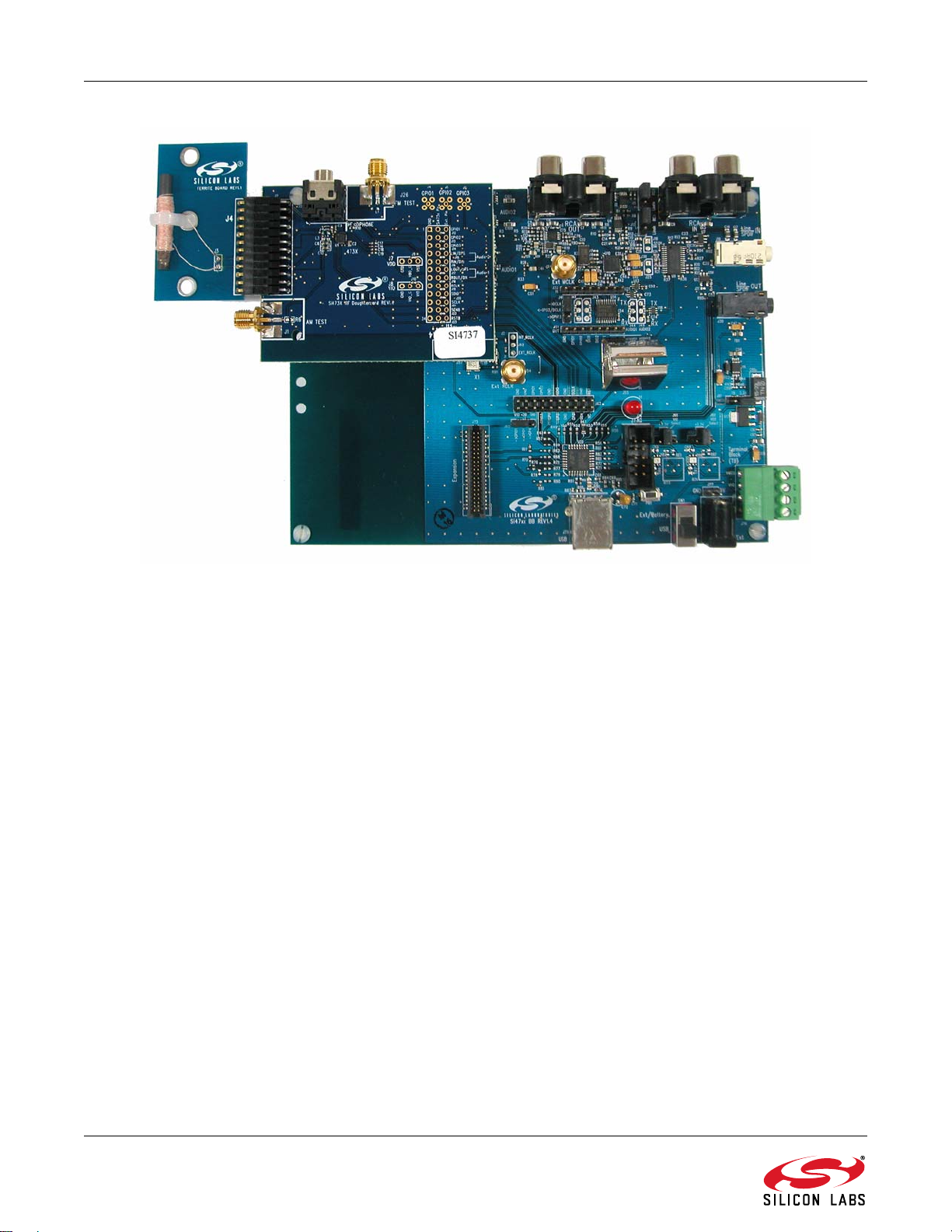
Si4737 AM/FM/WB Receiver with RDS
Si4738 FM/WB Receiver
Si4739 FM/WB Receiver with RDS
Si4740
Si4741
Si4742
Si4743
Si4744
Si4745
Si4749
1
AM/FM Receiver
1
AM/FM Receiver with RDS
1
AM/LW/SW/FM/WB Receiver
AM/LW/SW/FM/WB Receiver with
1
RDS
1
AM/LW/SW/FM Receiver
1
AM/LW/SW/FM Receiver with RDS
1
High-Performance RDS Receiver
Si4784 FM Receiver
RDS
FM Receiver
FM Transmitter
AM Receiver
WB Receiver
SW/LW Receiver
RPS
SAME
Digital Input
Digital Output
High Performance RDS
2
Embedded FM antenna
Package Size (mm)
AEC-Q100 Qualified
3x3
3x3
3x3
3x3
3x3
3x3
4x4
4x4
4x4
4x4
4x4
4x4
4x4
3x3
Si4785 FM Receiver with RDS
Notes:
1. Si4706, Si4707, and Si474x are covered under NDA.
2. High Performance RDS is available in Si4705/31/35/85-D50 and later.
2 Rev. 0.8
2
3x3

Si47xx-EVB
TABLE OF CONTENTS
1. Introduction . . . . . . . . . . . . . . . . . . . . . . . . . . . . . . . . . . . . . . . . . . . . . . . . . . . . . . . . . . . . .1
2. Description . . . . . . . . . . . . . . . . . . . . . . . . . . . . . . . . . . . . . . . . . . . . . . . . . . . . . . . . . . . . . .8
2.1. Si47xx Baseboard . . . . . . . . . . . . . . . . . . . . . . . . . . . . . . . . . . . . . . . . . . . . . . . . . . . .8
2.2. Si47xx Daughtercards . . . . . . . . . . . . . . . . . . . . . . . . . . . . . . . . . . . . . . . . . . . . . . . .15
3. Recommended Hardware Setup . . . . . . . . . . . . . . . . . . . . . . . . . . . . . . . . . . . . . . . . . . . .28
3.1. Hardware Setup for FM Transmitter Test . . . . . . . . . . . . . . . . . . . . . . . . . . . . . . . . .28
3.2. Hardware Setup for FM or Weather Band Receiver Test . . . . . . . . . . . . . . . . . . . . .29
3.3. Hardware Setup for AM Receiver Test . . . . . . . . . . . . . . . . . . . . . . . . . . . . . . . . . . .30
4. Getting Started . . . . . . . . . . . . . . . . . . . . . . . . . . . . . . . . . . . . . . . . . . . . . . . . . . . . . . . . . .32
4.1. Software Installation . . . . . . . . . . . . . . . . . . . . . . . . . . . . . . . . . . . . . . . . . . . . . . . . .32
4.2. Board Initialization . . . . . . . . . . . . . . . . . . . . . . . . . . . . . . . . . . . . . . . . . . . . . . . . . . .33
4.3. Switching Functions . . . . . . . . . . . . . . . . . . . . . . . . . . . . . . . . . . . . . . . . . . . . . . . . .36
4.4. State Management . . . . . . . . . . . . . . . . . . . . . . . . . . . . . . . . . . . . . . . . . . . . . . . . . .37
4.5. Disconnecting the EVB . . . . . . . . . . . . . . . . . . . . . . . . . . . . . . . . . . . . . . . . . . . . . . .39
5. FM Transmitter GUI . . . . . . . . . . . . . . . . . . . . . . . . . . . . . . . . . . . . . . . . . . . . . . . . . . . . . .40
5.1. Configuring the Si47xx as an FM Transmitter Using Analog Audio Input . . . . . . . . .40
5.2. Configuring the Si47xx as an FM Transmitter Using Digital Audio with
Analog Audio Source . . . . . . . . . . . . . . . . . . . . . . . . . . . . . . . . . . . . . . . . . . . . . . . . .41
5.3. Configuring the Si47xx as an FM Transmitter Using Digital Audio with
SPDIF Digital Source . . . . . . . . . . . . . . . . . . . . . . . . . . . . . . . . . . . . . . . . . . . . . . . .42
5.4. FM Transmitter Main Window . . . . . . . . . . . . . . . . . . . . . . . . . . . . . . . . . . . . . . . . . .43
5.5. FM Transmitter Settings (Analog Mode) Property Window . . . . . . . . . . . . . . . . . . . .45
5.6. FM Transmitter Settings (Digital Mode) Property Window . . . . . . . . . . . . . . . . . . . .47
5.7. CODEC Settings . . . . . . . . . . . . . . . . . . . . . . . . . . . . . . . . . . . . . . . . . . . . . . . . . . . .49
5.8. SPDIF Settings . . . . . . . . . . . . . . . . . . . . . . . . . . . . . . . . . . . . . . . . . . . . . . . . . . . . .50
5.9. FM Transmitter Receive Power Scan
5.10. FM Transmitter Radio Data Service (RDS) . . . . . . . . . . . . . . . . . . . . . . . . . . . . . . .52
5.11. FM Transmitter Register Map Window . . . . . . . . . . . . . . . . . . . . . . . . . . . . . . . . . .60
6. FM Receiver GUI . . . . . . . . . . . . . . . . . . . . . . . . . . . . . . . . . . . . . . . . . . . . . . . . . . . . . . . . .61
6.1. Configuring the Si47xx as an FM Receiver . . . . . . . . . . . . . . . . . . . . . . . . . . . . . . . .61
6.2. FM Receiver Main Window . . . . . . . . . . . . . . . . . . . . . . . . . . . . . . . . . . . . . . . . . . . .62
6.3. FM Receiver Settings Property Window . . . . . . . . . . . . . . . . . . . . . . . . . . . . . . . . . .64
6.4. CODEC and SPDIF Settings . . . . . . . . . . . . . . . . . . . . . . . . . . . . . . . . . . . . . . . . . . .73
6.5. FM Receiver RDS Window . . . . . . . . . . . . . . . . . . . . . . . . . . . . . . . . . . . . . . . . . . . .74
6.6. FM Receiver RDS Settings . . . . . . . . . . . . . . . . . . . . . . . . . . . . . . . . . . . . . . . . . . . .77
6.7. FM UI Settings . . . . . . . . . . . . . . . . . . . . . . . . . . . . . . . . . . . . . . . . . . . . . . . . . . . . .79
6.8. FM Receiver RSSI/SNR Graph Window . . . . . . . . . . . . . . . . . . . . . . . . . . . . . . . . . .80
6.9. FM Receiver Register Map Window . . . . . . . . . . . . . . . . . . . . . . . . . . . . . . . . . . . . .81
6.10. FM Receiver Logging Tools . . . . . . . . . . . . . . . . . . . . . . . . . . . . . . . . . . . . . . . . . .82
6.11. FM Receiver Configuration Helper . . . . . . . . . . . . . . . . . . . . . . . . . . . . . . . . . . . . .83
7. Weather Band GUI . . . . . . . . . . . . . . . . . . . . . . . . . . . . . . . . . . . . . . . . . . . . . . . . . . . . . . .90
7.1. WB Receiver Initialization . . . . . . . . . . . . . . . . . . . . . . . . . . . . . . . . . . . . . . . . . . . . .90
7.2. Weather Band Main Window . . . . . . . . . . . . . . . . . . . . . . . . . . . . . . . . . . . . . . . . . . .91
Window . . . . . . . . . . . . . . . . . . . . . . . . . . . . .51
Rev. 0.8 3

Si47xx-EVB
7.3. Weather Band Settings Property Window . . . . . . . . . . . . . . . . . . . . . . . . . . . . . . . . .92
7.4. Weather Band Receiver RSSI/SNR Graph Window . . . . . . . . . . . . . . . . . . . . . . . . .94
7.5. Weather Band Receiver Register Map Window . . . . . . . . . . . . . . . . . . . . . . . . . . . .95
7.6. Weather Band Receiver SAME Event Data (Si4707 only) . . . . . . . . . . . . . . . . . . . .96
8. AM Receiver GUI . . . . . . . . . . . . . . . . . . . . . . . . . . . . . . . . . . . . . . . . . . . . . . . . . . . . . . . .97
8.1. AM Receiver Initialization . . . . . . . . . . . . . . . . . . . . . . . . . . . . . . . . . . . . . . . . . . . . .97
8.2. AM Receiver Main Window . . . . . . . . . . . . . . . . . . . . . . . . . . . . . . . . . . . . . . . . . . . .98
8.3. AM Receiver Property Settings Window . . . . . . . . . . . . . . . . . . . . . . . . . . . . . . . . .100
8.4. AM Receiver RSSI/SNR Graph Window . . . . . . . . . . . . . . . . . . . . . . . . . . . . . . . . .105
8.5. AM Receiver Register Map Window . . . . . . . . . . . . . . . . . . . . . . . . . . . . . . . . . . . .106
8.6. AM Receiver Logging Tools Info . . . . . . . . . . . . . . . . . . . . . . . . . . . . . . . . . . . . . . .107
8.7. AM Receiver Configuration Helper . . . . . . . . . . . . . . . . . . . . . . . . . . . . . . . . . . . . .108
9. Using the EVB with a 9 V Battery . . . . . . . . . . . . . . . . . . . . . . . . . . . . . . . . . . . . . . . . . .109
10. Debugging Guidelines for Si47xx EVB . . . . . . . . . . . . . . . . . . . . . . . . . . . . . . . . . . . . .110
11. Bill of Materials . . . . . . . . . . . . . . . . . . . . . . . . . . . . . . . . . . . . . . . . . . . . . . . . . . . . . . . .112
12. Schematics . . . . . . . . . . . . . . . . . . . . . . . . . . . . . . . . . . . . . . . . . . . . . . . . . . . . . . . . . . .124
12.1. Si47xx-EVB Baseboard Rev 1.6 . . . . . . . . . . . . . . . . . . . . . . . . . . . . . . . . . . . . . .124
12.2. Si471x/2x-EVB Daughtercard Rev 1.4 . . . . . . . . . . . . . . . . . . . . . . . . . . . . . . . . .131
12.3. Si473x-EVB Daughtercard Rev. 1.4 . . . . . . . . . . . . . . . . . . . . . . . . . . . . . . . . . . .133
12.4. Si474x–EVB Daughtercard Rev 1.3 . . . . . . . . . . . . . . . . . . . . . . . . . . . . . . . . . . .135
12.5. Si4749-EVB Daughtercard Rev 1.1 . . . . . . . . . . . . . . . . . . . . . . . . . . . . . . . . . . .137
12.6. Antenna Card Schematics . . . . . . . . . . . . . . . . . . . . . . . . . . . . . . . . . . . . . . . . . .139
13. Layout . . . . . . . . . . . . . . . . . . . . . . . . . . . . . . . . . . . . . . . . . . . . . . . . . . . . . . . . . . . . . . .141
13.1. Si47xx-EVB Baseboard Rev 1.6 . . . . . . . . . . . . . . . . . . . . . . . . . . . . . . . . . . . . . .141
13.2. Si471x/2x-EVB Daughtercard Rev 1.4 . . . . . . . . . . . . . . . . . . . . . . . . . . . . . . . . .144
13.3. Si473x-EVB Daughtercard Rev 1.4 . . . . . . . . . . . . . . . . . . . . . . . . . . . . . . . . . . . .147
13.4. Si474x-EVB Daughtercard Rev 1.3 . . . . . . . . . . . . . . . . . . . . . . . . . . . . . . . . . . . .150
13.5. Si4749-EVB Daughtercard Rev 1.1 . . . . . . . . . . . . . . . . . . . . . . . . . . . . . . . . . . .152
13.6. Antenna Cards . . . . . . . . . . . . . . . . . . . . . . . . . . . . . . . . . . . . . . . . . . . . . . . . . . .155
Documentation Change List . . . . . . . . . . . . . . . . . . . . . . . . . . . . . . . . . . . . . . . . . . . . . . . .163
Contact Information . . . . . . . . . . . . . . . . . . . . . . . . . . . . . . . . . . . . . . . . . . . . . . . . . . . . . . .164
4 Rev. 0.8

Si47xx-EVB
This user's guide contains information related to only the Si47xx EVBs itemized in Table 2. Table 2 serves as a
quick reference guide for the sections of interest for your EVB. Sections 1, 4, 9, and 10 of the document apply to all
EVBs.
Table 2. Quick Reference Guide
Part Description Recommended
HW Setup
Si4704/05/
06/84/85
Si4707
Si4710/11/
12/13
Si4720/21 Sections 2.1.,
Si4730/31 Sections 2.1.,
Si4734/35 Sections 2.1.,
Si4736/37 Sections 2.1.,
Sections 2.1.,
2.2.1., and
2.2.6.
Section 2.2.2.,
2.2.5., 2.2.6.
Sections 2.1.,
2.2.1., 2.2.6.
2.2.1., 2.2.6.
2.2.2., 2.2.5.,
2.2.6
2.2.2., 2.2.5.,
2.2.6.
2.2.2., 2.2.5.,
2.2.6.
Section 3.2. Section 6. Section 11. Tables
Section 3.2. Section 7. Section 11.,
Section 3.1. Section 5. Section 11. Tables
Sections 3.1.
and 3.2.
Sections 3.2.
and 3.3.
Sections 3.2.
and 3.3.
Sections 3.2.
and 3.3.
GUI Bill of Materials Schematics Layout
Sections 12.1.,
Sections 5.
and 6.
Sections 6.
and 8.
Sections 6.
and 8.
Sections 6.,
7., and 8.
29 and 30
Tables 29 and 31
29 and 30
Section 11. Tables
29 and 30
Section 11. Tables
29, 31, 34, 35, and
36
Section 11. Tables
29 and 37
Section 11. Tables
29 and 37
12.2.
Section 12.1.,
12.3.
Sections 12.1.,
12.2.
Sections 12.1.,
12.2.
Sections 12.1.,
12.3., 12.6.1.,
12.6.2.
Sections 12.1.,
12.3., 12.6.3.
Sections 12.1.,
12.3., 12.6.3.
Sections
13.1., 13.2.
Section
13.1., 13.3.
Sections
13.1., 13.2.
Sections
13.1., 13.2.
Sections
13.1., 13.3.,
13.6.1.,
13.6.2.
Sections
13.1., 13.3.,
13.6.3.
Sections
13.1., 13.3.,
13.6.3.
Si4738/39 Sections 2.1.,
2.2.2., 2.2.5.,
2.2.6.
Si4740/41/
42/43/44/45
Si4749
Section 2.1.,
2.2.3., 2.2.5.,
2.2.6.
Sections 2.1.,
2.2.4. , 2.2.6.
Sections 3.2.
and 3.3.
Sections 3.2.
d 3.3.
an
Section 3.2. Section 6. Section 11. Tables
Sections 6.,
and 7.
Sections 7.
and 8.
Section 11. Tables
29 and 37
Section 11., Table
29, 32, 37
29 and 33
Sections 12.1.,
12.3., 12.6.3.
Sections 12.1.,
12.4., 12.6.4.
Sections 12.1.,
12.5.
Sections
13.1., 13.3.,
13.6.3.,
Sections
13.1.,
13.4.,13.6.4.
Section
13.1., 13.5.
Rev. 0.8 5

Si47xx-EVB
There are ten different EVB kits within the Si47xx family. Each kit ships with a standard set of components that are
common to all kits and a unique set that depends on the EVB kit P/N. Standard set of components are:
Customer welcome and evaluation letter
EVB Characterization Report
USB cable
RCA cable
9V battery
Headphones
Si47xx CD including:
Data sheet
Development application GUI rev 2.5.4 or later
User's guide
Quick start guide. The unique set of components for each EVB kit is defined in Table 3.
Table 3. Si47xx-EVB Kit Unique Contents
Adapters
EVB Kit Base
Board
Si4705-EVB
Si47xx
Base board
Rev1.3 or
Si4706-EVB
Si47xx
Base board
Rev1.3 or
Si4707-EVB
Si47xx
Base board
Rev1.3 or
Si4713-EVB
Si47xx
Base board
Rev1.3 or
Si4721-EVB
Si47xx
Base board
Rev1.3 or
Si4731-EVB
Si47xx
Base board
Rev1.3 or
later
later
later
later
later
later
Daughtercard Antenna
Cards
Si471x/2x
——YesNoNoNo
Daughtercard
Rev1.2 or later
Si471x/2x
——YesNoNoNo
Daughtercard
Rev1.2 or later
Si473x
Daughtercard
SAME
antenna
Rev1.2 or later
Si471x/2x
——YesNoNoNo
Daughtercard
Rev1.2 or later
Si471x/2x
——YesNoNoNo
Daughtercard
Rev1.2 or later
Si473x
Daughtercard
Rev1.2 or later
4731 antenna
kit (large ferrite, medium
ferrite, air loop
transformer)
Antennas BNC
Male to
RCA
Female
Whip
Yes No No No
antenna
Loop
Yes No No No
antenna
SMA
Male to
BNC
Female
SMA
Female to
BNC Male
SMA
Male to
SMA
Male
6 Rev. 0.8

Table 3. Si47xx-EVB Kit Unique Contents (Continued)
Si47xx-EVB
Adapters
EVB Kit Base
Board
Si4735-EVB
Si4737-EVB
Si4743-EVB
Si4749-EVB
Si47xx
Base board
Rev1.3 or
Si47xx
Base board
Rev1.3 or
Si47xx
Base board
Rev1.3 or
Si47xx
Base board
Rev1.3 or
later
later
later
later
Daughtercard Antenna
Cards
Si473x
Daughter
Card Rev1.2
or later
Si473x
Daughter
Card Rev1.2
or later
Si474x
Daughter
Card Rev1.3
or later
Si4749
Daughter
Card Rev1.0
or later
SW antenna Whip
WB antenna Whip
Antenna
Dummy
—Whip
Antennas BNC
Male to
RCA
Female
Yes No No No
antenna
Yes No No No
antenna
Whip
antenna
antenna
Yes Yes No Yes
Yes No Yes No
SMA
Male to
BNC
Female
SMA
Female to
BNC Male
SMA
Male to
SMA
Male
Rev. 0.8 7
Si47xx-EVB
J79 SW1 J78
J76
J74 PB1
J69
J68
J61
J30
J6
J52
X1
J54
J57
J27
J75
U22 D1
J77
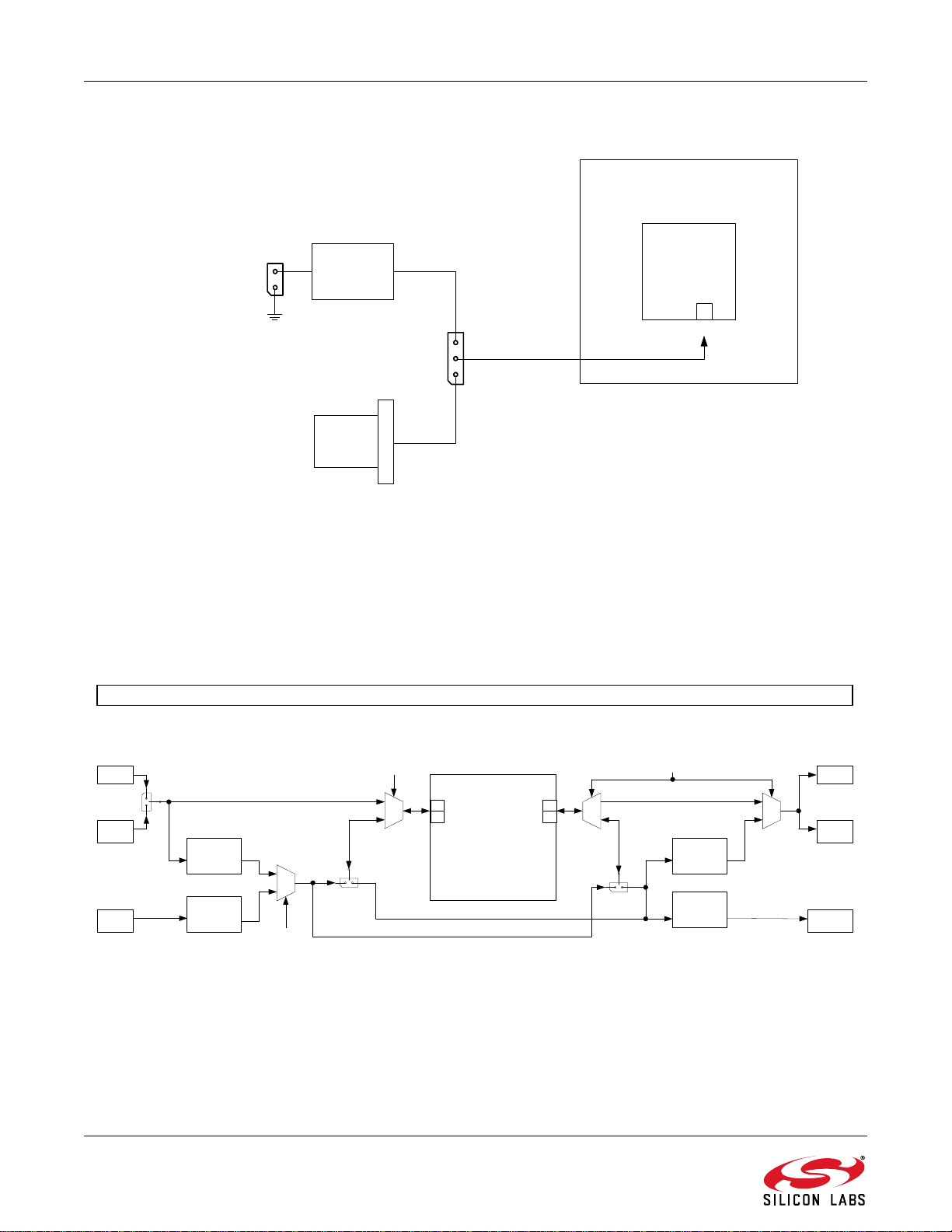
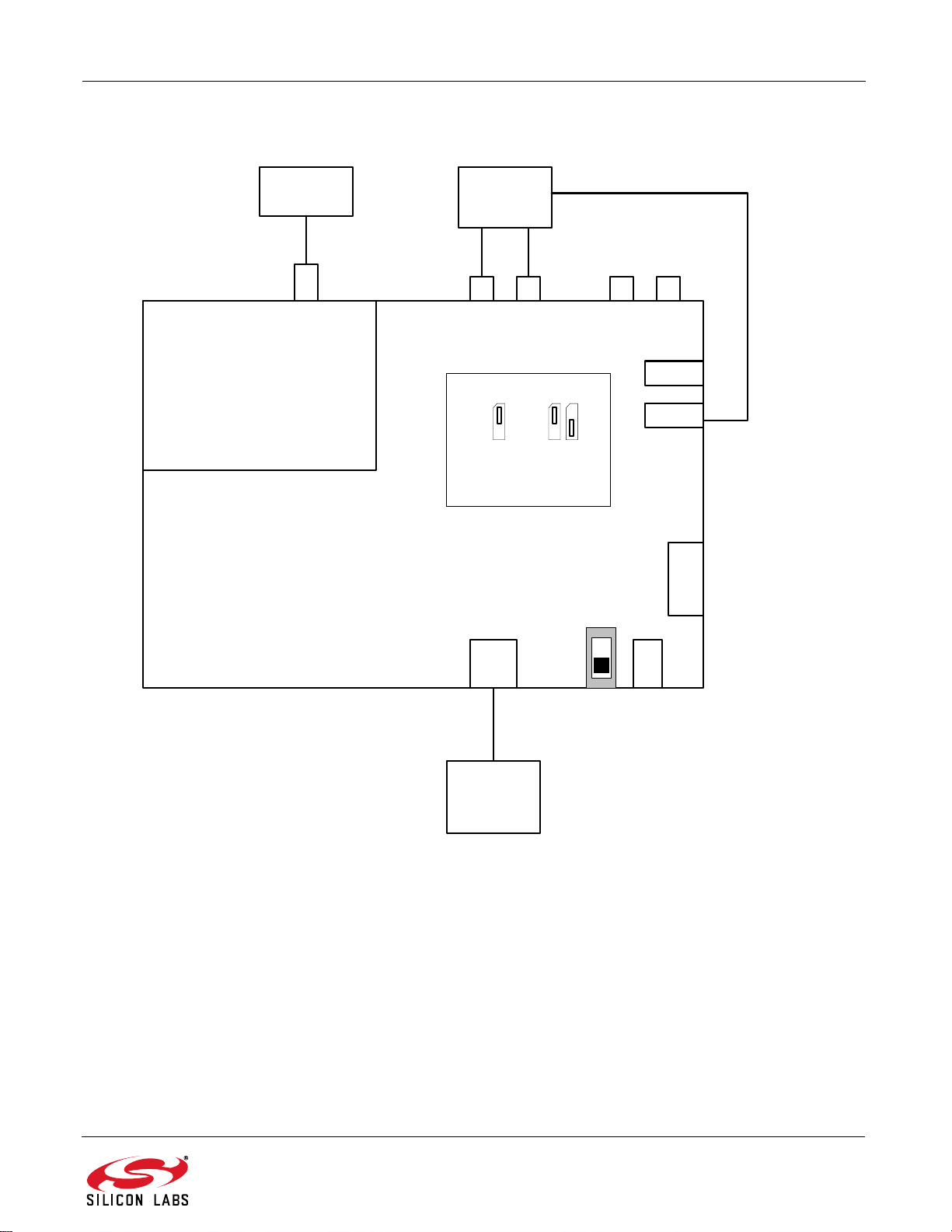
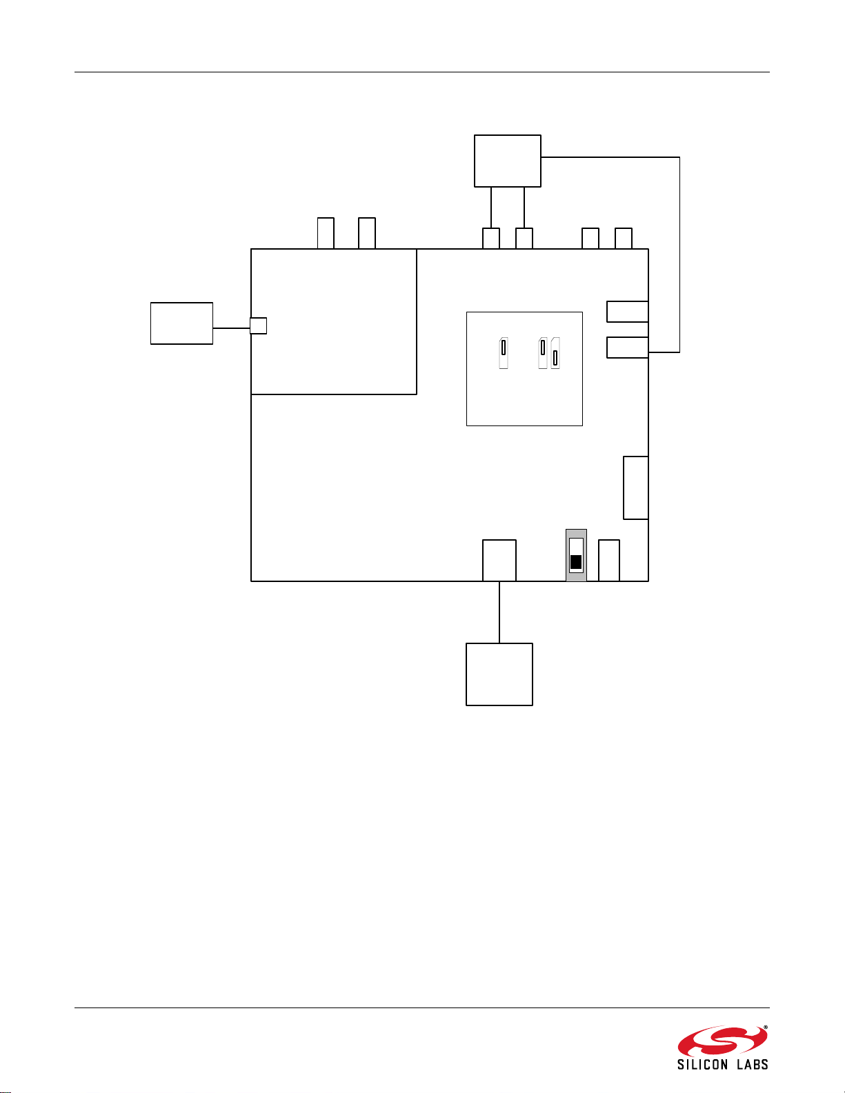
2. Description
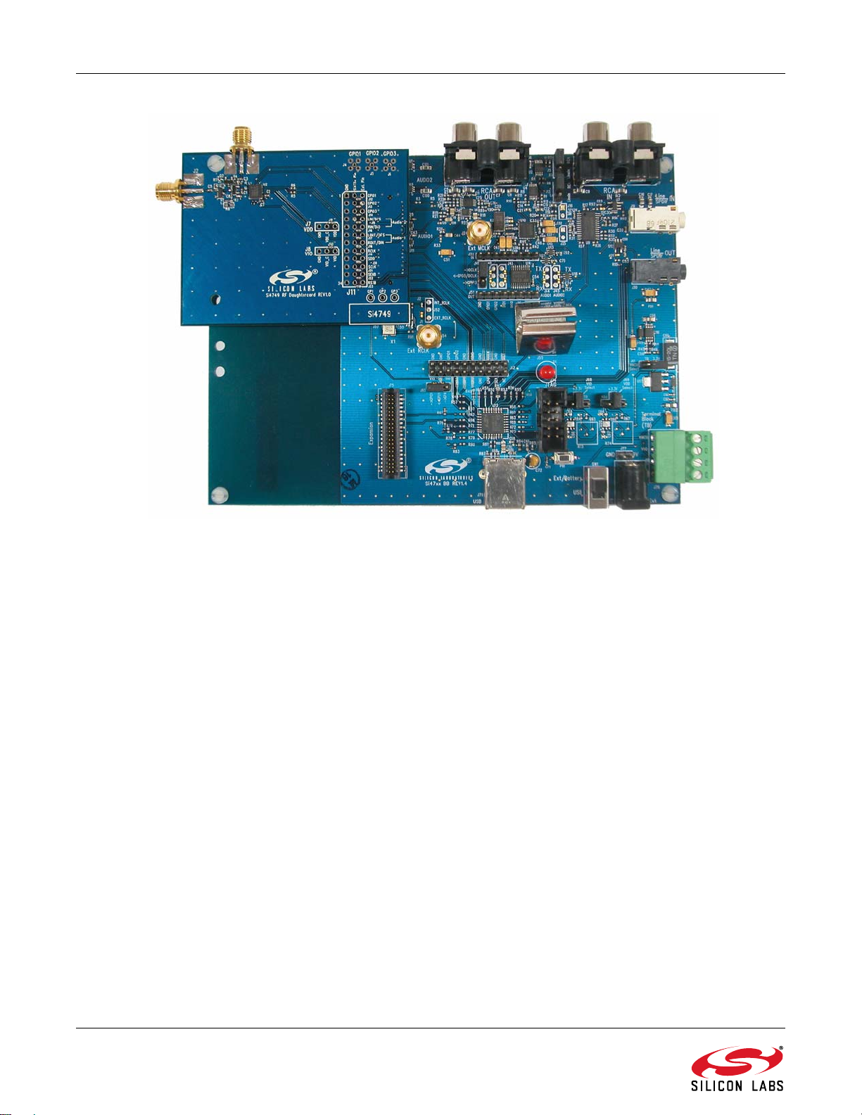
Si47xx EVB consists of a baseboard, a daughtercard with the Si47xx part pre-mounted, and, if applicable, an
antenna card. The baseboard is common and shared among all Si47xx EVBs. The following sections refer to both
the images in the figures and the silkscreen on the Si47xx EVB. Please refer to both when using this guide.
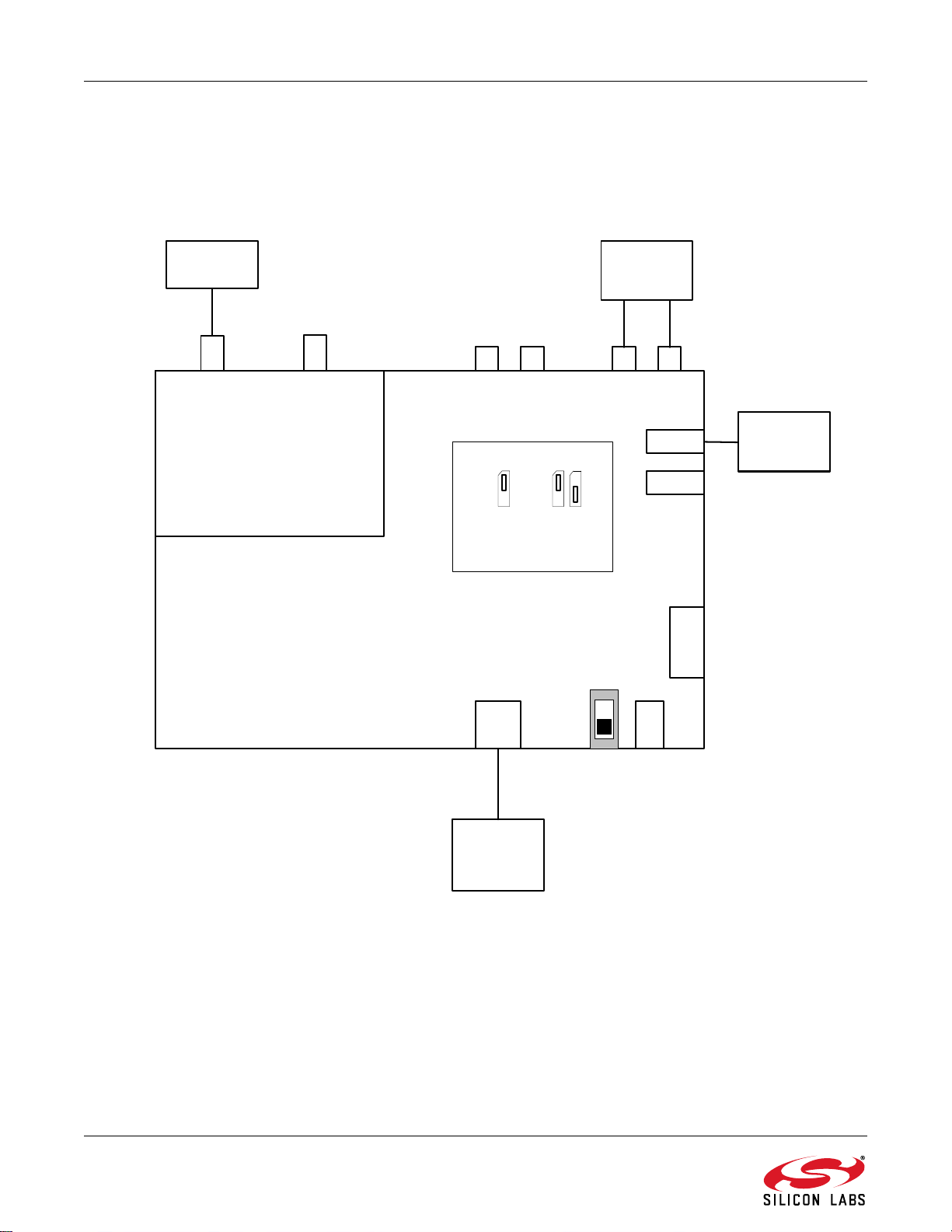
2.1. Si47xx Baseboard
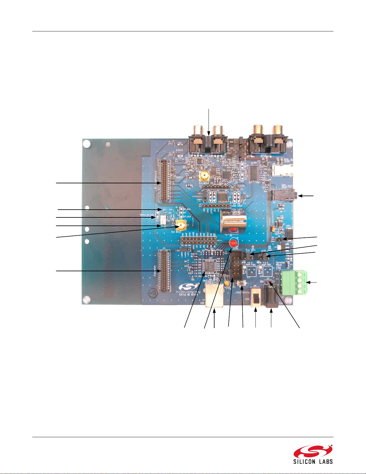
Figure 1. Baseboard Connectors, Jumpers, and Devices
Baseboard power connectors/devices:
J79 USB connector (using USB power)
J78 External power connector
J77 Battery connector
J76 Terminal block (TB) power connector
SW1 Switch to select between USB power or Ext power
J61 Jumper: Baseboard power select (3.3 V or TB)
J68 Jumper: Si47xx VIO power select (3.3 V or adjustable voltage via R73 or TB)
J69 Jumper: Si47xx VDD power select (3.3 V or adjustable voltage via R74 or TB)
8 Rev. 0.8
Baseboard audio I/O connectors:
SW1
J78
EXT
LDO
1.25–3.9 V
(R73)
LDO
1.25–7 V
(R74)
Jumper
J68
Jumper
J69
Daughterboard
Si47xx
VIO
10
11
VDD
ADJ
TB
+3.3 V
LDO
+3.3 V
(U17)
J79
USB
J76
Terminal
Block (TB)
Gnd
Vdd
Vio
Vm
ADJ
+3.3 V
TB
+3.3 V
TB
Vmcu
Jumper
J61
VIO
VDD
J77
BATT
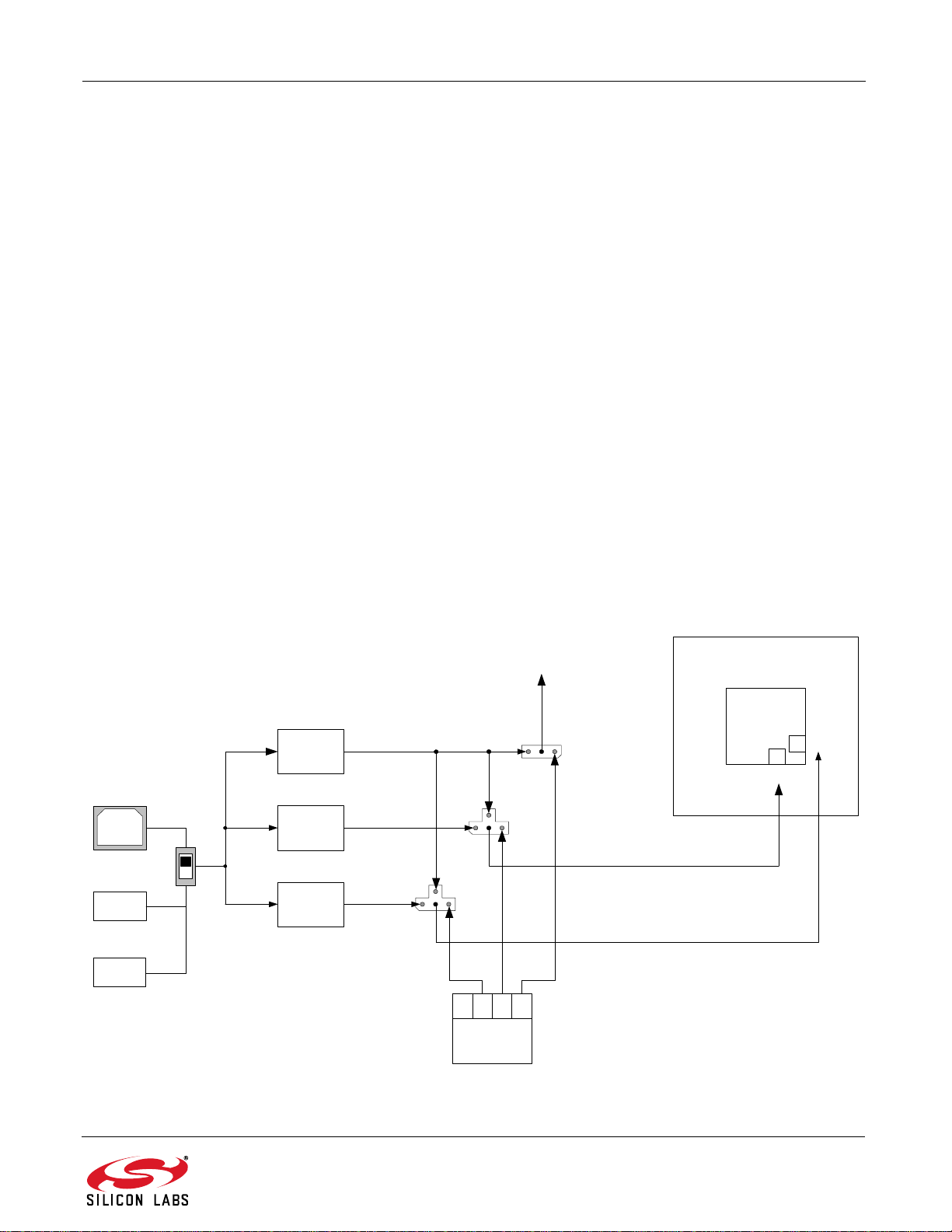
J6 RCA output
J30 Line output
Note: Line output will not be supported on new EVBs as of February 14, 2011.
Baseboard clock connectors/devices:
X1 32.768 kHz crystal oscillator
J52 Solder bump: select internal RCLK from oscillator
J54 Ext RCLK SMA connector input
J57 Jumper: Enable or Disable Int RCLK
Baseboard MCU connectors/devices:
U22 C8051F342 MCU
J79 USB connector to communicate with the MCU
J74 JTAG connector for the MCU
PB1 Push button to reset the MCU
D1 LED to confirm power supply to the MCU
Si47xx-EVB
Baseboard to Daughtercard connectors:
J27 Si47xx daughtercard connector
J75 Expansion card connector (reserved)
2.1.1. Power Supply Network
Figure 2. Power Supply Block Diagram
Rev. 0.8 9
Si47xx-EVB
J69J68
J61
ADJ
+3.3V
TB
ADJ
+3.3V
TB
+3.3V
TB
Vio Vdd Vmcu
ADJ
+3.3V
TB
+3.3V
TB
ADJ
+3.3V
TB
J69
J68 J61
Vio Vdd Vmcu
The Si47xx EVB can be powered using one of the following power supply options:
1. USB power supply via J79
2. External dc (Ext DC) power supply via power jack J78 or battery via J77
3. Three separate power supplies (Vdd, Vio, Vmcu) via terminal block J76
The EVB has three supply rails: Vdd, Vio, and Vmcu. Vdd and Vio are routed directly to the daughtercard to power
the Vdd and Vio pins on the Si47xx chip, while Vmcu is used to power the baseboard.
The external dc power supply and battery should not be connected simultaneously. Refer to Section 9. "Using the
EVB with a 9 V Battery‚" on page 109 for more information.
USB Power Supply & EXT DC Power Supply
Switch SW1 is used to select between the USB power supply and Ext dc power supply.
The USB power supply or the Ext dc power supply can be configured in one of the following two modes:
1. Fixed +3.3 V
2. Adjustable Vdd and Vio
Fixed +3.3 V
Only one LDO is used in this mode which outputs a +3.3 V supply to all three rails (Vdd, Vio, and Vmcu). The
jumpers need to be set according to Figure 3 to use the EVB in this configuration. This is the default configuration
on the EVB.
Terminal Block Power Supply
If the terminal block supplies are used, then jumpers J61, J68, and J69 need to be set according to Figure 4. The
user then needs to connect three different power supp lies for Vdd, Vio, and Vmcu.
Figure 3. Default Fixed +3.3 V Jumpers Setting
Figure 4. Terminal Block Jumpers Setting
10 Rev. 0.8
2.1.2. Microcontroller
MCU
C8051F342
Si47xx
SEN~
6 7 8
5
19 18 17
SCLK
SDIO
GPO1
GPO2
GPO3/
DCLK
RST~
MS_SENB
MS_RSTB
MS_SCLK
MS_SDIO
S_GPO3/DCLK
MS_GPIO2
SD_GPO1
Daughterboard
MD_GPIO3
TC_BCLK
(reserved for digital Rx )
Jumper
J41
MD_GPIO1
MD_GP4
J74
JTAG
PB1
Reset
J79
USB
Jumper
J65
Si47xx-EVB
Figure 5. MCU Block Diagram
The Si47xx EVB uses a Silicon Laboratories' C8051F342 microcontroller to control the Si47xx and to provide USB
connectivity from the host PC (via connector J79). The LED D1 illuminates to confirm that power is being properly
supplied to the C8051F342 and firmware has loaded. Push-button PB1 manually reset s the C8051F342. Th e JTAG
connector J74 is used to program the C8051F342 at production time, and is not required thereafter.
Rev. 0.8 11
Si47xx-EVB
Daughterboard
Si47xx
RCLK
9
X1
32.768 kHz
INT RClk
Jumper
J52
J54
EXT
RClk
Jumper
J57
DIS_INT_RCLK
INT_RCLK
EXT_RCLK
Note: Jumper J44 and J45 are automatically configured in EVB Rev 1.3.
Jumper
J5&J13
EVB In (TX only) 47xx Audio2 47xx Audio1 EVB Out (RX only)
1
0
0
1
CODEC OUT
DIN
LINE
OUT
CODEC IN
LINE
IN
DOUT
S/PDIF IN
SPDIF
IN
DOUT
S/PDIF OUT
DIN
SPDIF
OUT
0
1
0
1
Jumper
J45
TX: Analog/Digital In TX: Analog In TX: Digital In RX: Analog/Digital Out
RX: Digital Out RX: Analog Out
AUDIO2
To_TX
From_RX
AUDIO1
From_RX
To_TX
Jumper
J44
RCA In
Line In
(white)
SPDIF In
(white)
RCA Out
Line Out
(black)
SPDIF Out
(black)
Si47xx
(Daughterboard)
LIN/ DFS2
RIN/ DOUT
LOUT/ DFS1
ROUT/ DIN
14
13
AUDIO1
AUDIO2
15
16
J7
J19
J19
J6
J30
J30
Audio2
Select
Audio1
Select
Digital Input
Select
2.1.3. Reference Clock
Figure 6. Reference Clock Block Diagram
The Si47xx accepts a 32.768 kHz reference clock at the RCLK pin. On the EVB, this clock is provided by a
precision crystal oscillator. The user has the option of not using the onboard oscillator and bringing in the reference
clock from an external source through SMA connector J54.
When the user chooses to provide an external RCLK, jumper J52 has to be set accordingly. The user has the
option to turn off the onboard crystal oscillator by installing jumper J57.
2.1.4. Audio I/O
12 Rev. 0.8
Figure 7. Audio I/O Block Diagram

Si47xx-EVB
The EVB supports three different kinds of configurations for the FM transmitter:
Analog In to Analog In
Analog In to Digital In
Digital In to Digital In
Analog In to Analog In: This configuration provides a way for the user to evaluate the analog audio input for FM
transmission.
The input to the EVB is an analog audio provided via the RCA input connector J7 or LINE In connector J19 (white).
Jumpers J5 and J13 are set to RCA input by default. The user has to change this jumper accordingly if LINE In is
being used. Then the analog audio inpu t is routed directly through a switch to the Si47xx Rin/Lin inputs pin 15 and
16 (Audio2).
Analog In to Digital In: This configuration provides a way for the user to evaluate the Si4 7xx digit al audio input for
FM transmission using an analog audio input.
The input to the EVB is an analog audio provided via the RCA input connector J7 or LINE In connector J19 (white).
Jumpers J5 and J13 are set to RCA input by default. The user has to change this jumper accordingly if LINE In is
being used. Then the analog audio input is converted by CODEC U10 to a serial audio digital data before it is
routed to the Si47xx digital audio input DIO and DFS pin 13 and 14 (Audio1). The DCLK input is routed to the
GPO3/DCLK pin 17. Make sure that jumper J41 is set to DCLK to ensure proper operation.
Digital In to Digital In: This configuration provides a way for the user to evaluate the Si47xx digital audio input for
FM transmission using S/PDIF digital audio commonly found in sound cards.
The input to the EVB is a digital S/PDIF data provided via the S/PDIF In connector J19 (white). The digital S/PDIF
input is converted by S/PDIF Translator U9 to a serial audio digital data before it is routed to the Si47xx digital
audio input DIO and DFS pin 13 and 14 (Audio1). The DCLK input is routed to the GPO3/DCLK pin 17. Make sure
that jumper J41 is set to DCLK to ensure proper operation.
Note: Digital in through J19 will not be supported on new EVBs as of February 14, 2011.
The EVB supports three different kinds of configurations for the FM receiver:
Analog Out to Analog Out
Digital Out to Digital and Analog Out
Dual Output (Digital and Analog Out)
Analog Out to Analog Out: This configuration provides a way for the user to evaluate the analog audio output for
receiver operation. The output of the Si47xx is routed to RCA output connector J6 and Line output connector J30.
Digital Out to Digital and Analog Out: This configuration provides a way for the user to evaluate the digital audio
output for FM and AM receive using either S/PDIF digital audio or analog audio through the onboard CODEC. The
Si47xx digital audio out is routed through the S/PDIF translator µ9 to S/PDIF output connector J30 and routed
through the CODEC to RCA output connector J6 and line output connector J30.
Note: Digital output through J30 will not be supported on new EVBs as of February 14, 2011.
Dual Output (Digital and Analog Out): This configuration provides a way for the user to evaluate the analog
audio out and digital audio using S/PDIF digital audio for FM and AM. The analog output of the Si47xx is routed to
RCA output connector J6 and line output connector J30 and the digital audio out is routed through the S/PDIF
translator to S/PDIF output connector J30.
Note: Digital output through J30 will not be supported on new EVBs as of February 14, 2011.
Rev. 0.8 13

Si47xx-EVB
IMPORTANT: Jumper Settings
Because of the many possibilities available to configure the EVB, ensure that these four jumpers are set
accordingly:
1. J41: GPO3/DCLK setting
2. J44: TX/RX setting for Audio1 I/O (automatically set by the GUI for baseboard 1.3 and later)
3. J45: TX/RX setting for Audio2 I/O (automatically set by the GUI for baseboard 1.3 and later)
4. J5, J13: Analog Audio Source, RCA or Line In
J41: GPO3/DCLK Setting
Upper—DCLK digital audio clock
Lower—GPO3 digital control signal
For configuring the Si47xx digital audio input, make sure that the jumper is set in the Upper position so that the
DCLK signal will be routed to the Si47xx.
J44: TX/RX Setting for Audio1 I/O (automatically set by the GUI for baseboard 1.3 and later)
Upper—Audio1 is set to FM transmit (pin 13 and 14 will be the digital audio input).
Lower—Audio1 is set for FM receive (pin 13 and 14 will be analog/digital audio output).
J45: TX/RX Setting for Audio2 I/O (automatically set by the GUI for baseboard 1.3 and later)
Upper—Audio2 is set to FM transmit (pin 15 and 16 will be the analog/digital audio input).
Lower—Audio2 is set for FM receive (pin 15 and 16 will be the digital audio output).
J5, J13: Analog Audio Source, RCA or Line In
Upper—RCA inputs are used for analog audio source.
Lower—Line inputs are used for analog audio source.
14 Rev. 0.8
2.2. Si47xx Daughtercards
2.2.1. Si471x/2x Daughtercard
Si47xx-EVB
Figure 8. Si471x/2x Daughtercard Connectors and Devices
Daughtercard Connectors and Components:
U1 Si472x FM Transceiver or Si470x FM Receiver or Si471x FM Transmitter
L2 Tuning Inductor
R2 0 resistor to connect FM TX output to 10 cm trace built-in antenna
C8 2 pF capacitor to connect FM TX output to J1 SMA connector
R4 50 termination resistor
J1 SMA connector for FM transmitter output or FM receiver input for embedded antenna
J2 Header for putting external antenna for FM transmitter or embedded antenna for FM receiver
J28 SMA connector for FM receiver input
J29 Headphone jack for FM receiver
Rev. 0.8 15
Si47xx-EVB
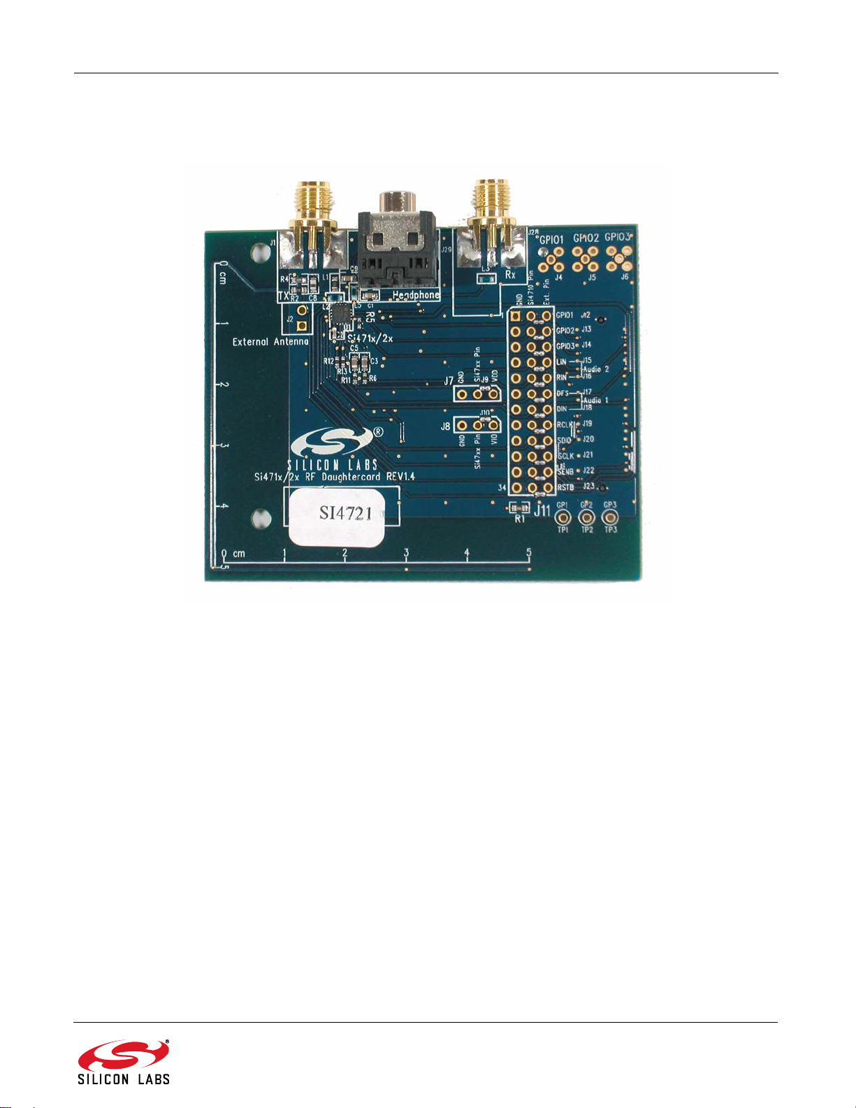
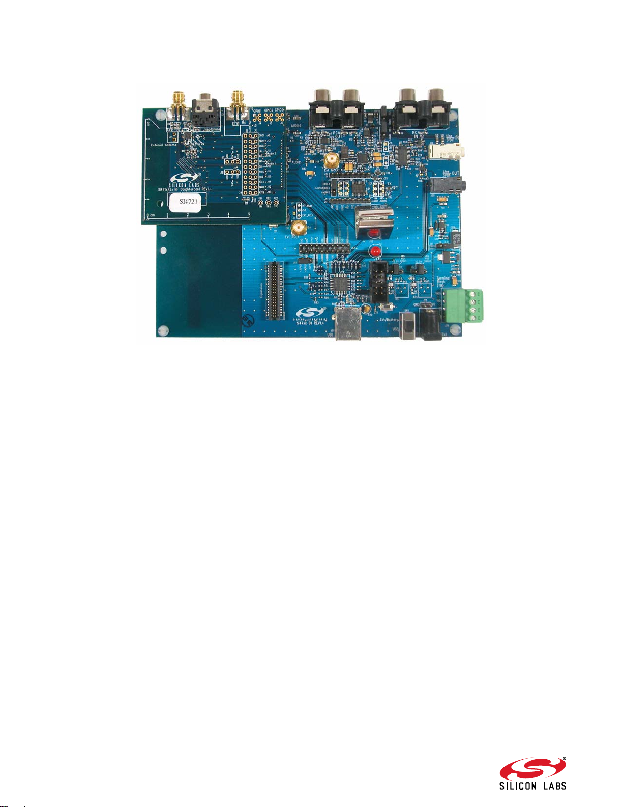
Figure 9. Fully Assembled Si471x/2x EVB
Si470x/1x/2x EVBs use Si471x/2x daughtercard with different population options depending on the individual
Si470x/1x/2x part. Please refer to individual Bill of Materials for each board.
16 Rev. 0.8
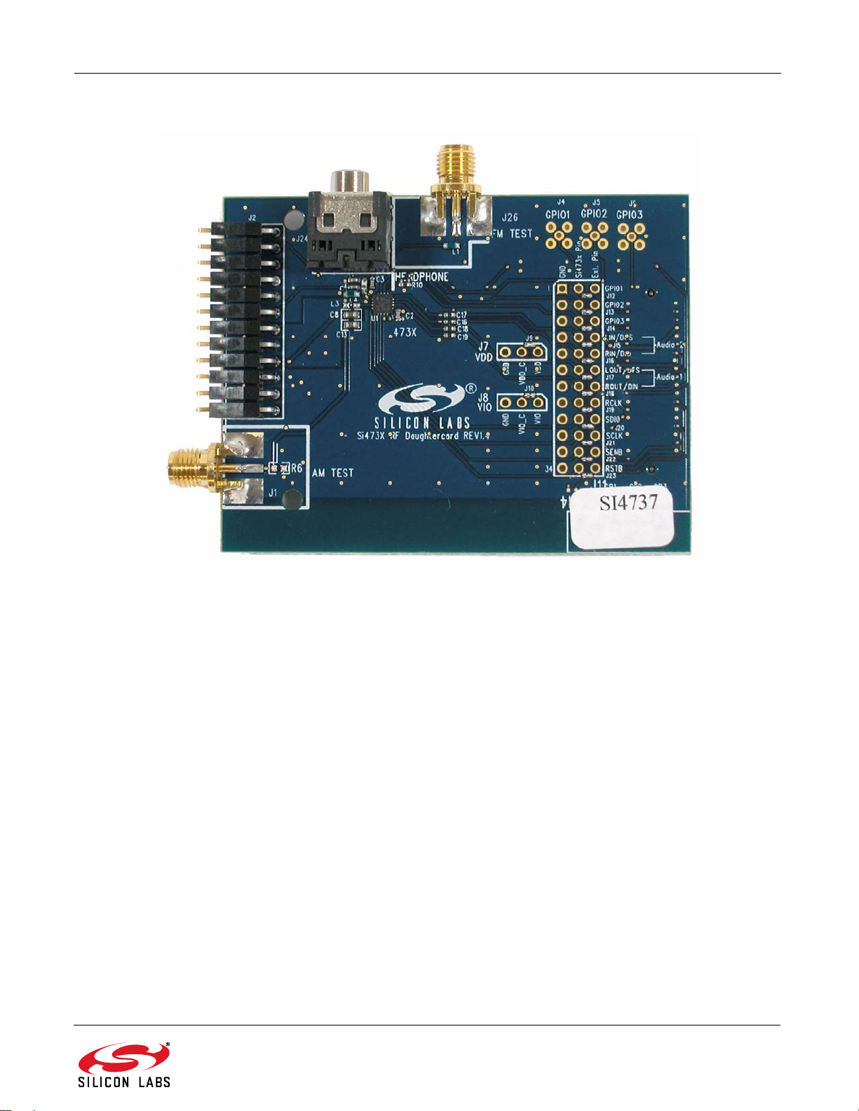
2.2.2. Si473x Daughtercard
Si47xx-EVB
Figure 10. Si473x Daughtercard Connectors and Devices
Daughtercard connectors and components:
J1 SMA connector for AM test circuit (does not apply to Si4707-EVB)
J2 Header for antenna interface connection
J24 Headphone jack
J26 SMA connector for FM test circuit
L4 270 nH inductor for FM input
U1 Si473x AM/FM/SW Weather Band Receiver chip (or Si4707 WB/Same receiver for Si4707-EVB only)
C2 Vdd bypass capacitor
C3 FM test circuit ac coupling capacitor
C8 AM input ac coupling capacitor
C12 FM input ac coupling capacitor
C13 AM test circuit ac coupling capacitor
Rev. 0.8 17
Si47xx-EVB
Figure 11. Fully Assembled Si473x-EVB with Ferrite Antenna Card
The Si473x/07 EVBs use Si473x daughtercard with different population options depending on the individual
Si473x/07 part. Please refer to individual Bill of Materials for each card.
Table 4 shows the antenna and audio connections for the Si47xx EVBs.
18 Rev. 0.8
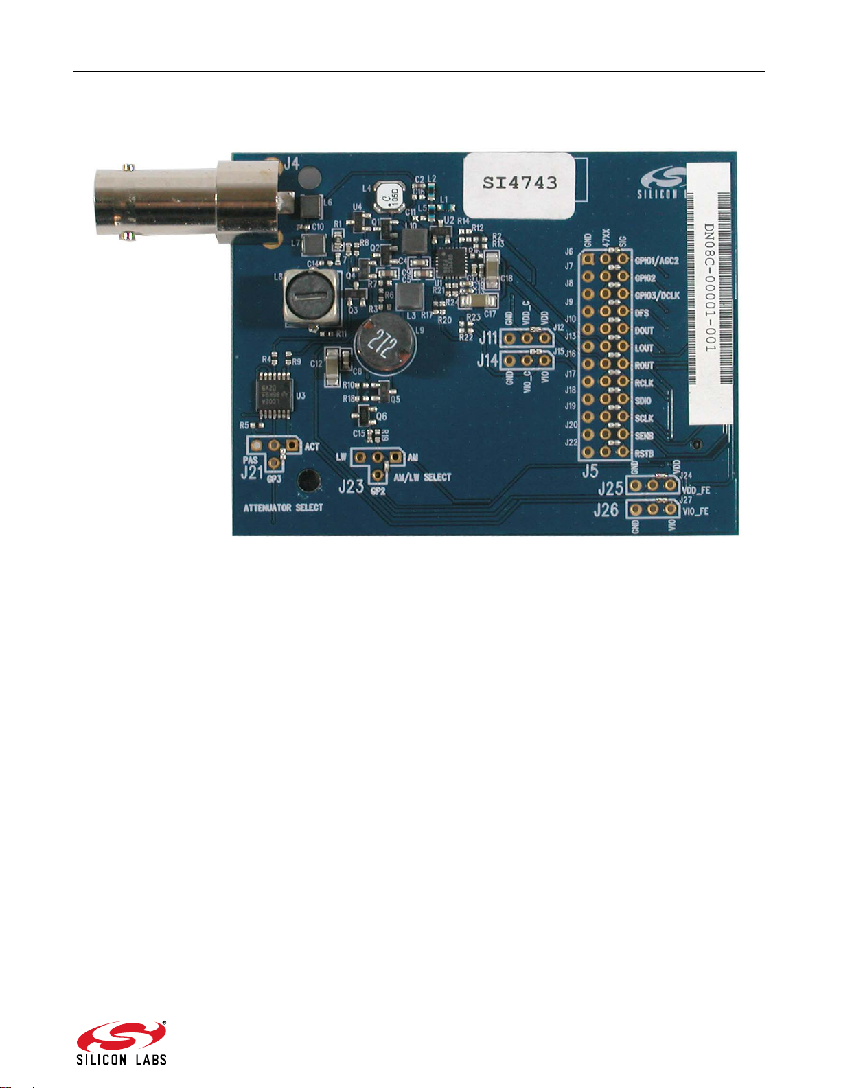
2.2.3. Si474x Daughtercard
Si47xx-EVB
Figure 12. Si474x Daughtercard Connectors and Devices
Daughtercard connectors and components:
J4 BNC connector for antenna connection
C6, C1, C18 Vdd bypass capacitor
C2 FM matching component
L1, L5 FM matching component
Q1–2 Cascode amplifier for AM front-end boost circuit.
U1 Si4740/41/42/43 AM/FM Receiver chip
The daughtercard implements the Si4740/41/42/43 AM/FM RDS receive solution.
The Si474x daughtercard also has a cascode amplifier circuit made up of two transistors to provide gain boost for
AM front-end. The on-chip De-Q resistors will then be used to adjust the overall circuit gain. In cases where the AM
reception is too strong, the front-end attenuators can be engaged by using GPIO1 as the control signal.
Rev. 0.8 19
Si47xx-EVB
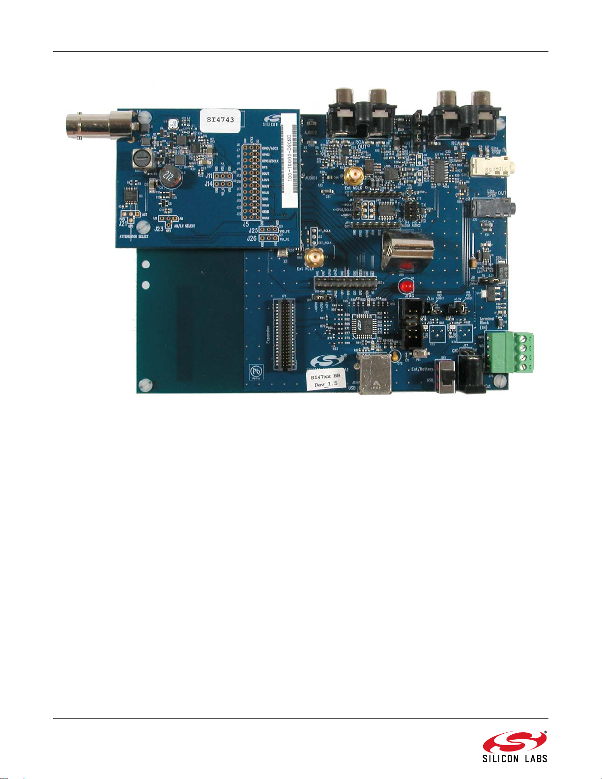
Figure 13. Fully Assembled Si474x-EVB
20 Rev. 0.8
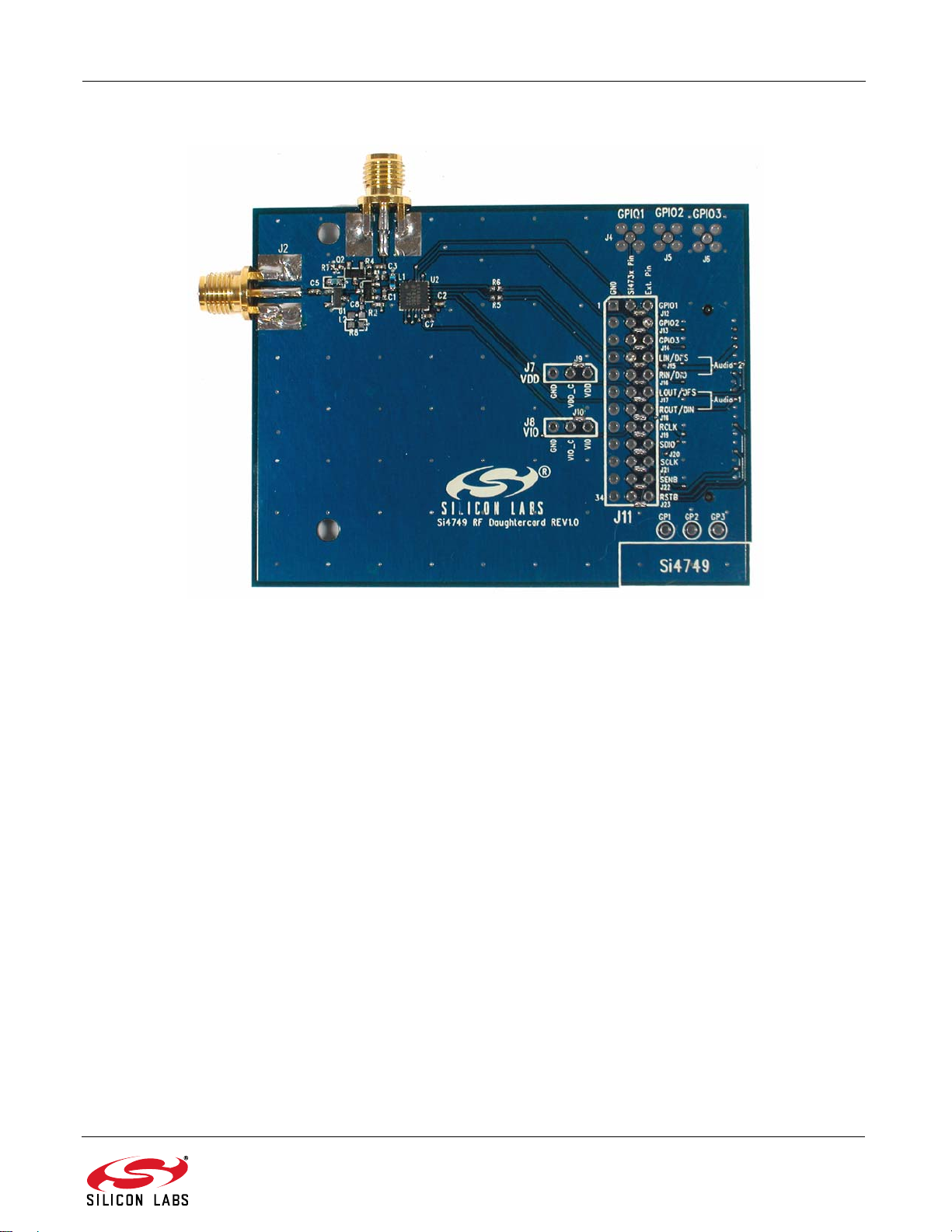
2.2.4. Si4749 Daughtercard
Si47xx-EVB
Figure 14. Si4749 Daughtercard Connectors and Devices
Daughtercard connectors and components:
J1 SMA connector for pass-thru FM connection
J2 SMA connector for FM antenna connection
C2 Vdd bypass capacitor
L1 FM matching component
U2 Si4749 RDS Receiver
The daughtercard implements the Si4749 RDS receive solution. The SMA connector, J2, allows the user to attach
a whip antenna for FM reception or a signal generator for FM test circuit. A pass-thru connection, J1, is also
present to provide the FM signal to other FM receivers if necessary.
Rev. 0.8 21
Si47xx-EVB
Figure 15. Fully Assembled Si4749-EVB
22 Rev. 0.8
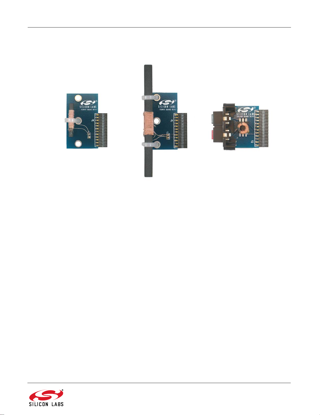
2.2.5. Antenna Interfaces
2.2.5.1. AM Antenna Interface
Si47xx-EVB
Figure 16. Antenna Board Options—SL4X30MW100T (Medium Ferrite), SL5X7X100MW70T (Large
Ferrite), and SL9X5X4MWTF Airloop
The user has the flexibility of choosing one of the two available antenna options. The user can either decide to use
the airloop antenna or the ferrite loop stick antenna.
Rev. 0.8 23
Si47xx-EVB
2.2.5.2. SW and Weather Band Antenna Interfaces
Figure 17. SW/WB Antenna Card (SW Population) and (WB Population)
The BNC connector, J2, will be used to connect a whip antenna for shortwave, FM, and weather band reception.
For SW reception, switch S1 must be in the SW position . The ferrite bar is used for AM reception, and the switch
S1 must be in the AM position for AM reception.
When using the WB Antenna Card, WB reception is through the whip antenna. For a better listening experience,
plug the headphones to J30 rather than J24.
Note: LW not supported with SW/WB Antenna Card.
2.2.5.3. Si474x Antenna Dummy Card
Figure 18. Si474x Antenna Dummy Card
24 Rev. 0.8

Table 4. Si47xx Antenna Connections
Si47xx-EVB
EVB Kit
Name
Si4705-X-
EVB
Si4706-X-
EVB
Si4707-B-
EVB
Si4713-B-
EVB
Si4721-B-
EVB
Si4731-X-
EVB
Si4735-X-
EVB
Si4737-X-
EVB
Receiver AM Antenna
Options
Si4705 None None Head-
Si4706 None None Head-
Si4707 None None None None Headphone J24
Si4713 None None Trace J2 None
Si4721 None None Head-
Si4731 SL5X7X100M
W70T Ferrite
/ Large Ferrite
SL4X30MW1
10T Ferrite /
Medium Fer-
rite
SL9X5X4MW
TF Autotrans-
former / Air
loop
Si4735 SL5X7X100M
W70T Ferrite
/ SW Antenna
card
Si4737 SL5X7X100M
W70T Ferrite
/ WB Antenna
card
AM
Connections
J2 Head-
J2
J2
J2 Head-
J2 Head-
FM
Antenna
Options
phone
Trace J2
phone
Trace J2
phone
Trace J2
phone
phone
Whip/SW
Antenna
Card
phone
Connections
FM
J29 None None
J29 None None
J29 None
J24 None
J24 Whip/SW
J2 For SW recep-
J24 None Headphone J24
SW Antenna
Options
Antenna Card
tion, set the
S1 switch to
SW position.
LW is not sup-
ported by the
SW antenna
card.
SW
Connections
J2
WB Antenna
Options
Whip/SAME
Antenna Card
Connections
WB
J2
Rev. 0.8 25

Si47xx-EVB
Table 4. Si47xx Antenna Connections (Continued)
EVB Kit
Name
Si4743-C-
EVB
Si4749-C-
EVB
Receiver AM Antenna
Options
Si4743 Whip / Si474x
Antenna
Dummy card
Si4749 None None Whip J2 None
AM
Connections
J4 Whip J4 Whip
FM
Antenna
Options
Whip/WB
Antenna
Card
FM
Connections
J2 Whip/WB
SW Antenna
Options
Connections
SW
WB Antenna
Options
Antenna Card.
For WB reception, set the S1
switch to WB
position
Connections
Table 5. Si47xx Audio Connections
EVB Kit Name Receiver Audio Out Options Audio Out Connections Audio In Options Audio Connections
Si4705-X-EVB Si4705 Headphone J29 None None
Unity Gain Buffer / RCA J6 (Baseboard)
Si4706-X-EVB Si4706 Headphone J29 None None
Unity Gain Buffer / RCA J6 (Baseboard)
Si4707-B-EVB Si4707 Headphone J29 None None
Unity Gain Buffer / RCA J6 (Baseboard)
Si4713-B-EVB Si4713 None None Unity Gain Buffer / RCA J7 (Baseboard)
WB
J2
Si4721-B-EVB Si4721 Headphone J29 Unity Gain Buffer / RCA J7 (Baseboard)
Unity Gain Buffer / RCA J6 (Baseboard)
Si4731-X-EVB Si4731 Headphone J24 None None
Unity Gain Buffer / RCA J6 (Baseboard)
Si4735-X-EVB Si4735 Headphone J24 None None
Unity Gain Buffer / RCA J6 (Baseboard)
Si4737-X-EVB Si4737 Headphone J24 None None
Unity Gain Buffer / RCA J6 (Baseboard)
Si4743-C-EVB Si4743 Unity Gain Buffer / RCA J6 (Baseboard) None None
Si4749-C-EVB Si4749 None None None None
26 Rev. 0.8

2.2.6. Test Circuit Interfaces
Table 6 shows the test circuit interface connections for Si47xx EVBs.
Table 6. Si47xx Test Circuit Connections
Si47xx-EVB
EVB Kit Name Receiver AM/SW/LW
Test
Options
Si4705-X-EVB Si4705 None None FMI / SMA J28 through C1.
Si4706-X-EVB Si4706 None None FMI / SMA J28 through C1.
Si4707-B-EVB Si4707 None None FMI / SMA J26 Unity Gain
Si4713-B-EVB* Si4713 None None LPI / SMA J1 None None Unity Gain
Si4721-B-EVB Si4721 None None FMI / SMA J28 through C1.
Si4731-X-EVB Si4731 AMI / SMA J1 through
Si4735-X-EVB Si4735 AMI / SMA J1 through
Si4737-X-EVB Si4737 AMI / SMA J1 through
Si4743-C-EVB Si4743 AMI / BNC J4 FMI / BNC J4 Unity Gain
Si4749-C-EVB Si4749 None None FMI / SMA J2 None None None None
AM/SW/LW
Connections
C13, remove
C8 for best
sensitivity
C13, remove
C8 for best
sensitivity
C13, remove
C8 for best
sensitivity
FM Test
Options
LPI / SMA J1
LPI / SMA J1
LPI / SMA J1
FMI / SMA J26 through C3.
FMI / SMA J26 through C3.
FMI / SMA J26 through C3.
FM Connections Audio Out
Remove C9 for
best sensitivity
Remove C9 for
best sensitivity
Remove C9 for
best sensitivity
Remove C12 for
best sensitivity
Remove C12 for
best sensitivity
Remove C12 for
best sensitivity
Test Options
Unity Gain
Buffer / RCA
Unity Gain
Buffer / RCA
Buffer / RCA
Unity Gain
Buffer / RCA
Unity Gain
Buffer / RCA
Unity Gain
Buffer / RCA
Unity Gain
Buffer / RCA
Buffer / RCA
Audio Out
Connections
J6 (Baseboard) None None
J6 (Baseboard) None None
J6 (Baseboard) None None
J6 (Baseboard) Unity Gain
J6 (Baseboard) None None
J6 (Baseboard) None None
J6 (Baseboard) None None
J6 (Baseboard) None None
Audio In
Test
Options
Buffer / RCA
Buffer / RCA
Audio In
Connections
J7
J7
*Note: The FM RF output will be available through the SMA connector J1. Refer to Table 7.
Table 7. FM Band Attenuation Factors
Frequency (MHz) Attenuation (dB)
76 32.13
88 30.91
98 30
108 29.2
Rev. 0.8 27
Si47xx-EVB
Si471x/2x
Daughterboard
RF
Analyzer
Analog
Audio
Generator
PC
w/ USB
port
J28
RCA OUT
USB
FM IN
J6
J79
USB Cable
SMA Cable
RCA Cable
EXT pwr
USB pwr
EXT Jack
SW1
Terminal
Block (TB)
J76
J78
Si47xx
Baseboard
J1
FM OUT RCA IN
J7
J19
J30
S/PDIF
Audio
Generator
J44 J45
Jumpers
Setting
J41
TX
RX
TX
RX
DCLK
GPIO3
Note: J44 and J45 are
automatically configured in
EVB Rev1.3 and later
3. Recommended Hardware Setup
The Si47xx-EVB can be configured for FM transmit, FM receive, WB receive, or AM/SW/LW receive. The following
is a description of how to correctly configure the device for either mode of operation.
3.1. Hardware Setup for FM Transmitter Test
Figure 19. Hardware Setup for FM Transmitter Test
Instructions for Si471x/2x daughtercards:
1. Connect the USB cable from PC to the EVB USB connector J79. The USB connection will serve as a dual purpose:
supplying the power to the EVB and controlling the EVB.
2. Connect an analog audio generator to the RCA input connector J7 using an RCA cable or connect an SPDIF digital audio
generator to connector J19 using an SPDIF cable.
3. Connect an RF analyzer from the FM output SMA connector J1 using an SMA cable.
4. J19 and J30 S/PDIF connections are no longer supported on EVBs as of February 14, 2011.
28 Rev. 0.8
3.2. Hardware Setup for FM or Weather Band Receiver Test
Si47xx
Daughterboard
RF
Generator
Audio
Analyzer
PC
w/ USB
port
J28 or J26
RCA OUT
USB
FM IN
J6
J79
USB Cable
SMA Cable
RCA Cable
EXT pwr
USB pwr
EXT Jack
SW1
Terminal
Block (TB)
J76
J78
J44 J45
Jumpers
Setting
J41
TX
RX
TX
RX
DCLK
GPIO3
Note: J44 and J45 are
automatically configured in
EVB Rev1.3 and later
Si47xx
Baseboard
RCA IN
J7
J19
J30
Optical
Cable
S/PDIF
OUT
Si47xx-EVB
Figure 20. Hardware Setup for FM/Weather Band Receiver Test
Instructions for Si4704/05/06/2x/3x/8x daughtercards:
1. Connect the USB cable from PC to the EVB USB connector J79. The USB connection will serve as a dual purpose,
supplying the power to the EVB and controlling the EVB.
2. Connect an audio analyzer from the RCA output connector J6 using an RCA cable.
3. Connect an RF generator to the FM input SMA connector J28 or J26 using an SMA cable.
4. Connect an audio analyzer to the S/PDIF output connector, J30, using an optical cable.
5.
To avoid possible sources of interference, please remove C9 or C12 (depending on the daughtercard). This will
disconnect the headphone circuit from the test circuit.
6. J19 and J30 S/PDIF connections are no longer supported on EVBs as of February 14, 2011.
Rev. 0.8 29
Si47xx-EVB
Si473x
Daughterboard
RF
Generator
Audio
Analyzer
PC
w/ USB
port
J28 or J26
RCA OUT
USB
F M IN
J6
J79
USB Cable
SMA Cable
RCA Cable
EXT pwr
USB pwr
EXT Jack
SW1
Terminal
Block (TB)
J76
J78
J44 J45
Jump ers
Se ttin g
J41
TX
RX
TX
RX
DCLK
GPIO3
Note: J44 and J45 are
automatically configured in
EVB Rev1.3 and later
Si47xx
Baseboard
J24
RCA IN
J7
J19
J30
Optical
Cable
S/PDIF
OUT
J1
3.3. Hardware Setup for AM Receiver Test
Instructions for Si473x daughtercards.
1. Connect the USB cable from PC to the EVB USB connector, J79. The USB connection will not only allow controlling of the
EVB, but will also provide power to the EVB.
2. Connect either the ferrite antenna or the airloop antenna board. The user also has the option of using the AM test input for
characterization by connecting the AM test input connector J1 to an RF generator source.
3. Connect an audio analyzer to the RCA output (connector J6) using an RCA cable for the analog audio output.
4. Connect an audio analyzer to the S/PDIF output (connector J30) using an optical cable.
5. Or, connect the headphone output to J24 on the daughtercard.
6. J19 and J30 S/PDIF connections are no longer supported on EVBs as of February 14, 2011.
Figure 21. Hardware Setup for AM Receiver Test (Si473x)
30 Rev. 0.8

Si47xx-EVB
Si47xx
Baseboard
Si474x
Daughterboard
RF
Generator
Audio
Analyzer/
Amplifier
PC
w/ USB
port
RCA OUT
USB
J79
USB Cable
RCA Cable
EXT pwr
USB pwr
EXT Jack
SW1
Terminal
Block (TB)
J76
J77
AM IN
J6
J19
J30
S/PDIF
OUT
Optical Cable
J4
Antenna
Dummy
AM Test Setup
Figure 22. Hardware Setup for AM Receiver Test (Si474x)
Instructions for Si474x daughtercards:
1. Connect the USB cable from PC to the EVB USB connector, J79. The USB connection will serve two purposes: supplying
the power to the EVB and controlling the EVB.
2. Connect a whip antenna to J4. The user has the option of using the AM test input for characterization by connecting the AM
test input connector J4 to an RF generator source through an antenna dummy.
3. Connect an audio analyzer to the RCA output (connector J6) using an RCA cable for the analog audio output.
4. Connect an audio analyzer to the S/PDIF output (connector J30) using an optical cable.
5. J19 and J30 S/PDIF connections are no longer supported on EVBs as of February 14, 2011.
Rev. 0.8 31

Si47xx-EVB
4. Getting Started
4.1. Software Installation
The Si47xx Windows GUI (graphical user interface) software is designed for use with the Si47xx evaluation board
(EVB). The GUI software revision number is available under Help
The GUI software development program uses a host machine USB port to communicate with the Si47xx EVB and
is tested for use with Windows XP, Windows 2000, and Windows 7.
To install, insert the Silicon Laboratories Si47xx CD into the host machine CD drive and launch Windows Explorer.
Open the CD to explore the contents in a window like the one shown in Figure 23.
About.
Figure 23. Installation and Setup Screen
Important: Open and read the Readme.doc file at this point. It may contain information that is not captured here,
and which could be very important to the functionality of the EVB or software.
Run the Setup.Exe and follow the instructions on the screen.
Note: If you get this Error message: "This setup requires the .NET Framework version 4.0," then you sho uld install the .NET
Framework that is provided on the CD and re-run the setup. The GUI requires version 4.0; however, multiple versions
such as 2.0, 3.0, and 5.0 can be installed simultaneously.
After installation is finished, a Silicon Labs Audio GUI icon will appear on your desktop. Launch the software by
clicking this icon on the desktop as shown in Figure 24.
Figure 24. Launching the GUI
32 Rev. 0.8

Si47xx-EVB
4.2. Board Initialization
After launching the GUI, you will be shown the initialization window as shown in Figure 25.
Note: This window can be accessed at any time by choosing Initialize from the File menu from the main GUI screen.
Figure 25. GUI Initialization Screen
4.2.1. Board Selection
At the top of the initialization window there is a board selection box, as displayed in Figure 26, that allows the
selection of the board that will be controlled by the GUI. This box is populated automatically and will update real
time as boards are connected/removed from the PC. If no EVBs are listed in the board selection box, verify that an
EVB is connected to the USB port of the PC running the GUI application.
After selecting the desired board the GUI will populate the rest of the dialog with options appropriate to the board
selected. You will only see modes/options for the type of board that is currently selected.
Figure 26. Board Selection Box
Rev. 0.8 33

Si47xx-EVB
4.2.2. Board Discovery Bus Mode
The initialize process can be configured to use either 2-wire or 3-wire bus mode. This can be configured by
selecting File
This feature is useful when using the Silabs EVB and GUI to control a prototype that is designed to use one bus
mode only.
4.2.3. Function Configuration
For each mode available on the selected EVB, multiple configuration items (Figure 27) will be present to allow for
configuration of the GUI software. It is possible to change these settings to meet testing requirements. The default
configuration of the board when you connect it to the computer is acceptable for most users. After initialization, the
GUI will save and restore these settings whenever the same type of board is connected.
Board Discovery Bus Mode.
Figure 27. Mode Configuration Items
4.2.3.1. Functions
Currently the UI supports four possible functions. These functions are AM Receiver, FM Receiver, WB Receiver,
and FM Transmitter.
Each function is configured independently from other functions. It is important to configure all functions as desired
as it is possible to have FM Receive boot in digital mode while AM Receive boots in analog mode.
The currently highlighted function row will be the function that is initialized when the Initialize button is selected.
Settings for other functions that are not selected will be saved and used to initialize that function when choosing
another function from the UI main window.
4.2.3.2. Boot Mode
There are two boot modes possible for each function. It is possible for some boot modes to not be available on
some boards.
From Device—This option will use the firmware embedded on the device selected. This is the faster of the
two options.
From File—This option will use the patch functionality of the device to send firmware from a file stored
within the UI to the device. If using this option, choose the appro priate firmware in the Firmware column fo r
the function you are configuring.
34 Rev. 0.8

Si47xx-EVB
4.2.3.3. Default Mode
There are two or more default modes possible for each function.
Use Last UI State: When selected, the GUI will restore all settings on the device to the previous settings
configured in the GUI the last time it was closed.
Use Chip Defaults: When selected, the GUI will use the settings that were default in the firmware on the
device. Only properties related to the corr ect setting of RCLK (such as frequ ency and prescaling) and initial
tuning (such as frequency) will be changed. If an error occurs during initialization of a function, choose this
setting to default the GUI settings back to the chip defaults.
Saved Configuration States: If you have previously saved or imported any configuration states, they will be
listed by name. When one of these is selected, the GUI will restore all settings on the device to the
previously saved settings.
4.2.3.4. Audio Mode
This option allows the user to change between Analog or Digital modes if the board connected supports digital.
Sections 2.1.4, 5, 6, and 7 each document the possible settings in more detail depending on what function is being
configured.
Figure 28 displays the window after the Details button has been pressed which helps with selection of the Audio
Mode by displaying a bitmap of the current audio setting in the dialog.
Figure 28. Expanded Details Dialog
4.2.3.5. Firmware
This selection is only required if "From File" was chosen for the Boot Mode. Use this setting to choose which
firmware will be downloaded to the device. If this item turns red then there is no firmware available for the function
so "From Device" must be chosen as the Boot Mode.
Rev. 0.8 35

Si47xx-EVB
4.2.3.6. Bus Mode
This setting affects all functions that are configured. It allows the device to be booted either in 2-wire or 3-wire
mode.
4.2.3.7. Internal Oscillator
When the "Use XOSCEN" is enabled and the board is configured to use the crystal oscillator, the GUI will boot the
device using the crystal oscillator. This option is only available on devices that support the crystal oscillator option.
4.2.3.8. Auto Boot when UI Opened and only One Board is Connected
When this item is selected, the GUI, when launched, will automatically boot the board if the same board is
connected. If more than one board is connected, the GUI will display the initialization dialog to allow selection of
the board to initialize.
4.3. Switching Functions
After the board has been properly configured for all functions it is possible to switch between functions from the
main UI window using the function buttons provided. Only function buttons will appear for the functions supported
by the device currently running. Figure 29 highlights the buttons used to switch functions from the main screen.
Figure 29. Function Switch Buttons
36 Rev. 0.8

Si47xx-EVB
4.4. State Management
Once the part has been initialized, a State Management option becomes available in the File Menu. This GUI
feature allows the user to save, retrieve, load, and delete the configuration state which contains the property
values.
4.4.1. Save Configuration State
To save the current configuration state, select File
Configuration window shown in Figure 30 will pop up. Enter a name for the configuration state and click OK. The
current state that contains the property values is now saved und er the given na me. If a st a te alre ady exist s with th e
chosen name, the GUI will give you the option of replacing the original state, entering a different name, or
canceling the save.
State ManagementSave Current State. The Select
Figure 30. Naming a Configuration State during Save
4.4.2. Retrieve Configuration State
Once a configuration state for a part has been saved, it will appear in the Default Mode list in the Initialization
window as shown in Figure 31. Select the state you wish to retrieve when initializing the part, and all properties and
the tuning frequency of the saved configuration will be restored.
Figure 31. Saved Configuration State
Rev. 0.8 37

Si47xx-EVB
4.4.3. Load Configuration State
When a configuration state for a part has been saved, it will also appear in the Load State list as shown in
Figure 32. Select the state you wish to load, and all properties and the tuning frequency of the saved configuration
will be restored without doing initialization to the chip.
Figure 32. Loading Configuration State
4.4.4. Delete Configuration State
To discard a saved configuration state, select File
window shown in Figure 33 will pop up. Select the configuration state you want to delete from the list and click OK.
The deleted configuration state will no longer be available in the Default Mode list of the Initialization window or
available for export.
State ManagementDelete State. The Delete Configuration
Figure 33. Selecting Configuration State to Delete
38 Rev. 0.8

Si47xx-EVB
4.4.5. Export Saved State
In addition to saving, retrieving, and deleting the configuration state, the GUI also gives the end user the ability to
export the configuration state to a file. The file can then be imported to installations of the GUI on different
machines to allow multiple users to easily implement the same configuration state. To export a saved configuration
state to a file, select File
as shown in Figure 34. Select the configuration state to export and click OK to save the configuration file with a .ini
extension. This configuration file can now be exported to different machines. The name of the saved state is
retained in the file when exported.
State ManagementExport Saved State and the Select Configuration window will pop
Figure 34. Selecting Configuration State to Export
4.4.6. Import Saved State
A saved configuration state can be imported from a .ini file exported by another instance of the GUI. To import a
saved state, select File
the file has been imported, the saved state will appear in the Default Mode list in the Initialization window. If a state
already exists with the same name as the state in the imported file, the GUI will give you the option of replacing the
original state, choosing a new name for the imported state, or canceling the import from file. The name appearing
in the initialization window will not necessarily be the same as the *.ini file name exported. It will reflect the name of
the original state that was exported.
State Management Import State File, then browse for and select the desired file. Once
4.5. Disconnecting the EVB
The GUI provides three methods for disconnecting the device: Closing the GUI, choosing disconnect from the file
menu, or physically disconnecting the device from the PC.
When closing the UI or selecting disconnect from the file menu, the GUI will prompt if the device should be
powered down or not. This prompt allows for further investigation of the device after the GUI has been
disconnected from the EVB. After the board has been disconnected through the File menu, the GUI will save the
current state of the device to disk. This state will be used to power up the device in the same state next time the
board is connected. The GUI will only save the current state if the board is disconnected through the File menu or
the GUI application is closed. If the board is removed from the PC without being disconnected through the File
menu and before the GUI is closed, then all state data will be lost.
Rev. 0.8 39

Si47xx-EVB
5. FM Transmitter GUI
The first Si47xx window is the Initialization window as shown in Figure 35.
Select the FM transmitter function.
As an FM transmitter, there are three audio input settings available:
Analog Input
Analog to Digital Input
Digital Input
5.1. Configuring the Si47xx as an FM Transmitter Using Analog Audio Input
This mode configures the Si47xx to receive analog audio input at pins 15 and 16 (LIN and RIN). The user has the
ability to provide analog audio from RCA In connector (J7) or Line In (J19). Set jumpers J5 and J13 accordingly.
Figure 35 shows the configuration setting for analog audio input. Configure the desired parameters in the
initialization screen and then click Initialize. A new window displaying "Initializing FM Transmitter" will appear.
Figure 35. Configuring the Si47xx to Transmit Analog Input
40 Rev. 0.8

Si47xx-EVB
5.2. Configuring the Si47xx as an FM Transmitter Using Digital Audio with Analog Audio
Source
This mode configures the Si47xx to receive digital audio input at pins 13 and 14 (DIN and DFS), but the user still
provides an analog audio source to the EVB. It is useful for a user who wants to test digital input on the Si47xx but
does not have a digital audio source. The analog audio source is converted to digital audio through the CODEC,
which can be configured to output various digital audio formats. Refer to Figure 41, “CODEC Settings Property
Window,” on page 49 to control the CODEC. Configure the desired parameters in the initialization screen and then
click Initialize. A new window displaying "Initializing FM Transmitter" will appear.
Figure 36. Configuring the Si47xx to Transmit Digital Input by Using Analog Source (CODEC)
Rev. 0.8 41

Si47xx-EVB
5.3. Configuring the Si47xx as an FM Transmitter Using Digital Audio with SPDIF Digital
Source
This mode configures the Si47xx to receive digital audio input at pin 13 and 14 (DIN and DFS) when the user has
an SPDIF digital audio source. The SPDIF source is converted to PCM digital audio by the SPDIF translator. Refer
to Figure 42, “SPDIF Settings Property Window,” on page 50 to control the SPDIF translator.
Note: The Si47xx requires the digital audio signal to be present when initializing the part. Therefore, connect the SPDIF IN
signal prior to initializing the part. SPDIF will not be supported on new EVBs as of February 14, 2011. This mode of
operation will not be available in the initialization window for those boards.
Figure 37. Configuring the Si47xx to Transmit Digital Input by Using Digital Source (SPDIF)
42 Rev. 0.8

5.4. FM Transmitter Main Window
1
2
3
4
5
6
7
8
9
11
10
12
13
14
15
16
17
18
19
20
21
22
23
24
25
26
The FM transmitter main window will appear after initialization.
Si47xx-EVB
Figure 38. FM Transmitter Main Window
Table 8. FM Transmitter Main Window Descriptions
# Description Range
1
Transmit frequency display. Enter the desired FM transmit frequency in this window.
2
Transmit voltag e display. Enter the desired FM transmit voltage in this window.
3
Varactor Value. This is an indicator showing the tuning cap value of the Si472x device.
Each number represents 0.25 pF. If the varactor value is manually overwritten in the
property window, the indicator will change from automatic mode to manual mode.
4
RF on or off. Selecting this checkbox will enable the FM transmit, while turning this button off will disable the FM transmit.
5
Pre-Emphasis. Click one of the three buttons to set the pre-emphasis e ither to Of f, 50 µs
or 75 µs.
6
Si472x EVB audio input setting indicator: Analog In/Digital (Analog In to CODEC)/Digital
(SPDIF).
7
Presets. Press and hold the desired preset button for 1.5 seconds to program. The current frequency will replace the preset number. Press for less than 1.5 seconds to tune to
the displayed frequency. Presets can also be programmed automatically from the
Receive Power Scan window.
8
Pilot Tone Generation. Set to 19 kHz and select "Pilot On" when in stereo mode. Set to
0–19 kHz for and select "Pilot On" for test tone generation.
9
Audio Deviation. Enter the desired audio deviation in this window.
10
Pilot Deviation. Enter the desired pilot deviation in this window.
76–108 MHz
88–120 dBuV
1–191
On/Off
Off, 50 µs, 75 µs
Analog, Digital
CODEC, Digital
SPDIF
76–108 MHz
0–19 kHz
0–90 kHz
0–90 kHz
Rev. 0.8 43

Si47xx-EVB
Table 8. FM Transmitter Main Window Descriptions (Continued)
# Description Range
11
RDS Deviation. Enter the desired RDS deviation in this window (Si4711/13/21 only).
12
Total Deviation. This is an indicator only displaying the sum of the audio, pilot and RDS
deviation. If the total deviation exceeds 75 kHz, the indicator will turn red and a warning
sign is displayed.
13
Input Mute Left/Right. Selecting this checkbox will mute the Left or Right audio channel.
14
Turn on or off th e pilot tone for stereo or mono FM transmit mode.
15
Turn on or off the RDS transmission (Si4711/13/21 only).
16
Modulation On. Selecting this checkbox will modulate the audio, pilot, and RDS signal
according to the audio, pilot, and RDS deviation. De-selecting this checkbox will turn off
modulation for all audio, pilot, and RDS signal and only the carrier will be transmitted.
17
Turn on or off th e L-R channel for stereo or mono FM transmit mode.
18
Turn on or off the compressor for the audio signal.
19
Attack time. Set the attack time for the compressor in milliseconds.
20
Release time. Set the release time for the compressor in milliseconds.
21
Threshold. Set the threshold for the compressor.
22
Input Gain. Set the compressor gain.
23
Limiter Release Time. Set the limiter release time constant.
(Not available in Si4710-A10).
24
Turn on or off the limiter feature.
25
Audio Level Indicators. Overmodulation, Limiter, Audio input level below low-level
threshold (silence detection), and Audio input level below high-level threshold (loud
detection). To enable these four indicators, check the Enable Interrupts box. These
indicators are sticky; to clear them, click the Reset button.
26
Mode switch buttons to switch between different modes on the device. See section 4 for
more information.
0–7.5 kHz
0–187.5 kHz
On/Off
On/Off
On/Off
On/Off
On/Off
On/Off
0.5–5 ms
100–1000 ms
–40 to 0 dBFS
0 to 20 dB
0.5,1,2,3,4,5,6,7,8,
9,10,20,30,40,50,
75,100 ms
On/Off
44 Rev. 0.8

Si47xx-EVB
5.5. FM Transmitter Settings (Analog Mode) Property Window
FM transmitter settings can be configured through the properties window by selecting WindowProperties.
Properties are grouped into categories which can be selected from the drop-down box in the upper right of the
window. For convenience, all FM transmitter properties are also located in Window
mode properties will be available if Analog Mode was selected in the initialization window.
PropertiesTX: All. Analog
Figure 39. FM Transmitter Settings in Analog Mode Property Window
Table 9. FM Transmitter Settings in Analog Mode Property Window Descriptions
Item Description Range Devices
Line Input
Attenuation (k)
Maximum Line Input
Level (mVpk)
Reference Clock
Frequency (Hz)
The Si47xx has four attenuator settings (636, 416,
301, and 190 mVp). It will tell the maximum audio
input signal that the user can give to the LIN and RIN
input. The attenuator setting will determine the audio
input impedance (LIN and RIN) of the device.
The maximum line input level of the max audio input
signal that the user supplies to the device. This number has to be less than or equal to the attenuation setting. The max line input level will correspond to the
max audio deviation set in the audio deviation window
on the main GUI. Make sure that the actual audio
input signal does not exceed this limit, otherwise the
audio signal will become distorted.
This field is used to specify the frequency of the
reference clock. The input to the RCLK pin divided by
the prescaler is the reference clock. The reference
clock must be in the range of 31130 to 34406 Hz.
190 mVp,
301 mVpk,
416 mVp,
636 mVpk
0–Line Input Attenu-
ation
31130–34406 Hz All
All
All
Rev. 0.8 45

Si47xx-EVB
Table 9. FM Transmitter Settings in Analog Mode Property Window Descriptions (Continued)
Item Description Range Devices
Reference Clock
Prescaler
Audio Level High
Duration (mSec)
Audio Level High
Threshold (dBFS)
Audio Level Low
Duration (mSec)
Audio Level Low
Threshold (dBFS)
Varactor Capacitor
Overwrite
This field is used to specify the prescaler value. The
input to the RCLK pin divided by the prescaler is the
reference clock. The reference clock must be in the
range of 31130 to 34406 Hz.
Set the duration for the audio level high before an
interrupt is generated.
An interrupt will be generated when the audio input
level rises above this threshold for the duration greater
than the Audio Level High Duration setting. This may
also be called loud detection indicator.
Set the duration for the audio level low before an interrupt is generated.
An interrupt will be generated when the audio input
level falls below this threshold for the duration greater
than the Audio Level Low Distortion setting. This may
be called silence detection indicator.
This field allows the user to manually overwrite the
tuning capacitance. A number 0 indicates that the
tuning cap is automatically adjusted. Any number
other than 0 (1 to 191) will indicate that the tuning cap
is manually adjusted.
1–4095 All
0–65535 All
–70 to 0 All
0–65535 All
–70 to 0 All
Automatic: 0,
Manual: 1–191
All
46 Rev. 0.8

Si47xx-EVB
5.6. FM Transmitter Settings (Digital Mode) Property Window
FM transmitter settings can be configured through the properties window by selecting WindowProperties.
Properties are grouped into categories which can be selected from the drop-down box in the upper right of the
window. For convenience, all FM transmitter properties are also located in Window
mode properties will be available if CODED or SPDIF modes was selected in the initialization window.
Properties TX: All. Digital
Figure 40. FM Transmitter Settings in Digital Mode Property Window
Table 10. FM Transmitter Settings in Digital Mode Property Window Descriptions
Item Description Range Applicable
Reference Clock
Frequency (Hz)
Reference Clock
Prescaler
Digital Format
Digital Sample
Precision
Digital Sample
Rate (Hz)
This field is used to specify the frequency of the reference clock. The input to the RCLK pin divided by the
prescaler is the reference clock. The reference clock
must be in the range of 31130 to 34406 Hz.
This field is used to specify the prescaler value. The
input to the RCLK pin divided by the prescaler is the
reference clock. The reference clock must be in the
range of 31130 to 34406 Hz.
2
S of left justified digital format.
Sets I
Select the precision of the digital audio input.
Sets the DFS digital sample rate. Must be set to 0 Hz
before DCLK/DFS is removed.
31130–34406 Hz All
1–4095 All
2
Left-Justified, I
DSP (MSB on first
DCLK), or DSP
(MSB on second
DCLK)
8, 16, 20, 24 bits All
0, 32000–
48000 Hz
S,
Devices
All except
Si4710-A10
All except
Si4710-A10
Rev. 0.8 47

Si47xx-EVB
Table 10. FM Transmitter Settings in Digital Mode Property Window Descriptions (Continued)
Item Description Range Applicable
Devices
Digital Mono
Mode Enable
Digital DCLK
Falling Edge
Audio Level Low
Threshold (dBFS)
Audio Level Low
Duration (mSec)
Audio Level High
Threshold (dBFS)
Audio Level High
Duration (mSec)
V aractor Capacitor
Overwrite
Select between Digital Stereo or Mono.
Select between using rising edge or falling edge of
DCLK when sampling Digital Input (DIN) data.
An interrupt will be generated when the audio input
level falls below this threshold for the duration greater
than the Audio Level Low Distortion setting. This may
be called silence detection indicator.
Set the duration for the audio level low before an
interrupt is generated.
An interrupt will be generated when the audio input
level rises above this threshold for the duration greater
than the Audio Level High Duration setting. This may
also be called loud detection indicator.
Set the duration for the audio level high before an
interrupt is generated.
This field allows the user to manually overwrite the
tuning capacitance. 0 indicates that the tuning cap is
automatically adjusted. Any number other than 0 (1 to
191) will indicate that the tuning cap is manually
adjusted.
On/Off All
On/Off All
–70 to 0 All
0–65535 All
–70 to 0 All
0–65535 All
Automatic: 0
Manual: 1–191
All
48 Rev. 0.8

Si47xx-EVB
5.7. CODEC Settings
In addition to other digital mode properties, a category of CODEC settings may configured by selecting
Window
PropertiesCODEC Settings if CODEC mode was selected in the initialization window.
Item Description Range
CODEC Precision
CODEC Output Format
CODEC Sampling Rate
CODEC Channel Swap
CODEC Invert Clock
Figure 41. CODEC Settings Property Window
Table 11. CODEC Settings Property Window Descriptions
Misc.
Select the CODEC digital audio output precision.
Select the CODEC digital audio format between I
fied, DSP (MSB on first DCLK), or DSP (MSB on second DCLK).
Select the sample rate of the CODEC digital audio output.
Select whether the CODEC digital output L-R data is normal or
swapped.
Select between using rising edge or falling edge of DCLK when
sampling Digital Input (DIN) data.
2
S, Left Justi-
16, 20, 24 bits
2
Left-Justified, I
(MSB on first DCLK), or
DSP (MSB on second
DCLK)
32 or 48 kHz
On/Off
On/Off
S, DSP
Rev. 0.8 49

Si47xx-EVB
5.8. SPDIF Settings
In addition to other digital mode properties, a category of SPDIF settings may be configured by selecting
Window
Note: SPDIF will not be supported on new EVBs as of February 14, 2011. These properties will not be available through the
PropertiesSPDIF Settings if SPDIF mode was selected in the initialization window.
GUI in conjunction with those boards.
Figure 42. SPDIF Settings Property Window
Table 12. SPDIF Settings Property Window Descriptions
Item Description Range
Misc.
SPDIF Invert Clock
SPDIF Output Format
50 Rev. 0.8
Select between using rising edge or falling edge of DCLK when
sampling Digital Input (DIN) data.
Select the SPDIF digital audio format between I
2
S or Left Justified.
On/Off
Left-Justified or I
2
S

Si47xx-EVB
5.9. FM Transmitter Receive Power Scan Window
The Receive Power Scan window enables the user to scan the entire FM band to find one or more candidate
channels on which to transmit, where candidate channels are defined as those with the lowest received power.
Selecting Window
and channel spacing can be selected and the number of regions can be set to return one to ten candidate
channels. The number of channels to average can be set to 1, 3, 5, or 7. Selecting “To Presets “will save the
candidate channels to the GU I presets. Refer to "AN307: Si4712/13/20/21 Receive Power Scan" for additional
information on the RPS feature and algorithm.
Power Scan will launch the Receive Power Scan Window as shown in Figure 43. The band
Figure 43. Receive Power Scan Window
Rev. 0.8 51

Si47xx-EVB
5.10. FM Transmitter Radio Data Service (RDS)
The RDS/RBDS feature is available with the Si4711/13/21. This user guide assumes that the user is already
familiar with the RDS/RBDS standard. If necessary, the user may refer to the following documents to become
familiar with the RDS/RBDS standard.
United States RBDS Standard by National Radio Systems Committee, April 9, 1998.
RDS Universal Encoded Communication Protocol Version 5.1 by European Broadcasting Union, August
1997.
Silicon Labs “AN243: Using RDS/RBDS with the Si4701/03.”
In order for the user to transmit RDS, check the RDS On box. Failure to turn on RDS means that the RDS data will
not be transmitted. The following picture illustrates the RDS On box that should be turned on.
Figure 44. Turning RDS On in the FM Transmitter Main Window
After the RDS transmission is enabled, click on WindowRDS Transmit Data to go to the RDS Transmit Data
screen. This window allows the user to configure RDS data to be transmitted and also allows the user to gain
insight to the Si4711/13/21 RDS capability.
52 Rev. 0.8

Si47xx-EVB
Item Description
RDS/RBDS Selection
Program Type (PTY)
PTY Dynamic
PI
Program Service Messages
Load Msgs
Repeat Count
Message Count
Mix
Alternate Frequency
Artificial Head
Figure 45. RDS Transmit Window
Table 13. RDS Transmit Window Descriptions
General
Select either RDS format (Europe) or RBDS format (US).
Select the available Program T ype (PTY) from the pulldown menu.
Select whether the PTY will be dynamic or static.
Enter Program Identification (PI) code here.
Program Service
Enter up to 12 different Program Service (PS) Messages. Each PS consists of a
maximum 8 characters. Messages are ordered left to right, top to bottom.
Load the PS messages into the device.
Enter how many time each PS will be repeated before sending the next PS.
Enter how many messages of the loaded PS that will be transmitted.
Select the mix percentage between transmitting the Program Service or Buffers.
Part of RDS Group Type 0 (PS): Enter Alternate Frequency if it is available.
Part of RDS Group Type 0 (PS): Enter whether Artificial Head is On or Off.
Rev. 0.8 53

Si47xx-EVB
Item Description
Stereo
Audio Compression
Traffic Program
Traffic Announcement
Speech
Radio Text
Radio Text: A/B Flag
Radio Text: Add to Circular
Radio Text: Add to FIFO
Manual Group Entry: B
Manual Group Entry: C
Manual Group Entry: D
Manual Group Entry: Add to
Circular
Manual Group Entry: Add to
FIFO
Circular
Circular: Size (Blocks)
Circular: Delete Group
Circular: Clear Buffer & Send
FIFO
FIFO: Size (Blocks)
FIFO: Add Time
FIFO: Delete Group
FIFO: Clear Buffer & Send
Table 13. RDS Transmit Window Descriptions
Part of RDS Group Type 0 (PS): Enter whether the transmitted audio is Stereo or
Mono.
Part of RDS Group Type 0 (PS): Enter whether the Audio Compression is On or Off.
Part of RDS Group Type 0 ( PS): Enter whether Traffic Program is available or not.
Part of RDS Group T ype 0 (PS): Enter wh ether T raf fic Announcement is available or
not.
Part of RDS Group Type 0 ( PS): Enter between Speech or Music transmission.
Buffers
Enter the RDS Group Type 2 Radio Text (RT) messages that will be loaded into
either the circular or FIFO buffer.
Part of RDS Group Ty pe 2 (RT): Enter whether the A/B Flag is set or not in entering
the RT. This A/B Flag will tell the receiver to clear the display when the flag toggles
from one state to the other.
Add the RT messages that are entered into the GUI circular buffer queue.
Add the RT messages that are entered into the GUI FIFO buffer queue.
Enter manual RDS entry block B. With this window , you can transmit all RDS Grou p
Types 0 throug h 15.
Enter manual RDS entry block C. With this window, yo u can transmit all RDS Group
Types 0 throug h 15.
Enter manual RDS entry block D. With this window, yo u can transmit all RDS Group
Types 0 throug h 15.
Add the RDS manual entry values into the GUI circular buffer queue.
Add the RDS manual values into the GUI FIFO buffer queue.
Indicator showing the GUI circular buffer queue.
Indicator showing the size (in blocks) of the circula r buffer. The total size of the
buffer is 128, which is shared between the circular and FIFO buffers. To adjust the
size, change the size in the FIFO buffers.
Delete the currently selected group in the GUI circular buffer queue.
Clear the circular buffer on the device and send the messages in the GUI circular
buffer queue to the device.
Indicator showing the GUI FIFO queue.
Indicator showing the size (in blocks) of the FIFO buffer. Adjusting the size of the
FIFO will also adjust the size of the circular buffer. The total of those two buffers is
128 blocks.
This will get the current time and format it into RDS Group Type 4 Clock & Time
(CT), and add it to the GUI FIFO buffer queue.
Delete currently selected group in the GUI FIFO buffer queue.
Clear the FIFO buffer on the device and send the message in the GUI FIFO buffer
queue to the device.
54 Rev. 0.8

Si47xx-EVB
There are 16 different group types in the RDS/RBDS standard, and for every group the following information is
always transmitted:
1. Program Identification (PI)
2. Program T ype (PTY)
The GUI makes it easy to send data in three of the following group types:
1. Group Type 0: Program Service (PS)
2. Group Type 2: Radio Text (RT)
3. Group Type 4: Clock Time (CT)
It is possible to send data in the other group types, but the user has to manually enter the data in hexadecimal
code.
Because of the complexity of the RDS/RBDS standard, the explanation of the RDS Transmit Data window is
divided into three sections: Basic, Intermediate, and Advanced.
Rev. 0.8 55

Si47xx-EVB
2
3
4
1
5
5.10.1. Basic
The RDS Transmit Window is divided into three categories:
1. General
2. Program Service
3. Buffers
In the basic section, we will cover two out of the three categories: the General and Program Service. In the General
category, the user can set the PI and PTY data. In the Program Service, the user can set the PS data (Group Type
0). The following diagram shows a step-by-step explanation:
Figure 46. Basic RDS Message Illustration
1. First select whether you want to transmit in RDS format (Eur op e) or RBDS fo rmat (US).
2. Type in the Program Identification in this field. Program Identification is a 16-bit code assigned to an
individual station.
3. Select the Program Type in the pull down menu here. Some examples include news, information, sports,
talk, rock, etc.
4. Enter the Program Service (PS) in the boxes provided. You can enter a maximum of 12 different PS
messages, in which each PS message can contain a maximu m of 8 char ac te rs.
a. Repeat Count: Enter how many times you want each PS message to be transmitted before sending
the next PS message.
b. Message Count: Enter how many of the 12 PS messages that you actually want to transmit.
c. Mix: Select 100 percent.
5. Click Send Message button here. Now the RDS will transmit the PS message along with the PI and PTY.
You should see these data in your RDS receiver.
56 Rev. 0.8

Si47xx-EVB
2
3
4
1
5
3a
6
5.10.2. Intermediate
In the intermediate section, we will cover the buffers category of sending the RDS data with the device, in particular
we will send Group Type 2 (Radio Text) and Group Type 4 (Clock Time).
The following diagram shows a step-by-step procedure to send the buffers data in addition to the General and
Program Service data covered in the basic section.
Figure 47. Intermediate RDS Message Illustration
1. Select the Mix percentage that you want between transmitting the data in Program Service and the data in
the Buffers. A mix percentage of 100% means that you will always transmit the PS message regardless of
what is contained in the Buffers, whereas a mix percentage of 0% means that you will always transmit the
data in the Buffers regardless of what is contained in the PS. If the buf fers are empty, the PS messages will
be transmitted all the time regardless of the mix percentag e.
2. Enter the Radio Text message that will be transmitted. After entering the RT message, click either the "Add
to Circular" button or the "Add to FIFO" button. The RT message will be encoded according to the RDS
Group Type 2 rule.
a. Clicking "Add to Circular" button means that you add the RT message into the GUI Circular Buffer
queue. Note that the message itself has not been uploaded into the Circular Buffer inside the device
until the Clear Buff & Send is clicked.
b. Clicking "Add to FIFO" means that you upload the RT message into the GUI FIFO Buffer queue. Note
3. Enter the size of the FIFO that you want here. The device buffer has a total of 128 blocks, which is shared
4. Clicking this "Clear Buff & Send" button will upload the message from the GUI Circular Buffer queue into
that the message itself has not been uploaded into the FIFO Buffer inside the device until the Clear
Buff & Send is clicked.
by the circular buffer and the FIFO. Therefore, the circular buffer size (shown in 3a) will be the remainder of
the 128 blocks minus the FIFO size.
the Circular Buffer inside the device. The Circular Buffer on the part will repeatedly send the message
contained in the buffer. Note that the messages in the circular buffer will be transmitted only if the PS Mix
Rev. 0.8 57

Si47xx-EVB
2
3
4
1
5
6
7
8
9
value is set to anything other than 100%.
5. Clicking the "Add Time" button here will add the current time as a RDS Group Type 4 message to the GUI
FIFO Buffer queue.
6. Clicking the "Clear Buff & Send" button will upload the message from the FIFO Buffer Indicator Window
into the FIFO Buffer inside the device. The FIFO Buffer on the part will only send the messages contained
in the buffer once. A good example of using FIFO buffer is when you want to send the time data. Time is
something that occurs only once, so it will not be beneficial to upload time to the circular buffer and transmit
it continuously. Refer to step 5 for information on sending time data. Note that the messages in the FIFO
buffer will be transmitted only if the PS Mix value is set to anything other than 100%.
5.10.3. Advanced
In the advanced section, we will cover the remaining RDS topics.
Figure 48. Advanced RDS Sending Illustration
1. Dynamic: This tells whether the PTY code is static or dynamic.
2. Alternate Frequency: This provides the ability to inform the receiver of a single alternate frequency. This
field is transmitted along with the Group Type 0 (PS).
3. Miscellaneous bits in Group Type 0 (PS):
a. Artificial Head: 0 = Not Artificial Head; 1 = Artificial Head
b. Stereo: 0 = Mono; 1 = Stereo
c. Audio Compressor: 0 = Not compressed; 1 = Compressed
d. Traffic Program (TP): 0 = No TP; 1 = TP
e. Traffic Announcement (TA): 0 = No TA; 1 = TA
f. Speech: 0 = Speech; 1= Music
4. A/B Flag: This is an important flag in the RDS Group Type 2 (RT). Checking this box when a Radio Text is
58 Rev. 0.8

Si47xx-EVB
uploaded means that the RT is uploaded with the flag set. Un-checking this box when an RT is uploaded
means that the flag is not set. This flag tells the receiver that when the flag togg les from set to r eset or vice
versa, the receiver will clear the display before showing the next RT.
5. Manual Group Entry: Use this box to upload the RDS data manually. You can use this box to upload
messages from the Group Type for which the GUI does not have encoding support. For these messages,
the user must encode the messages into hexadecimal code.
6. Circular Buffer Indicator: This displays the message that gets uploaded into the Circular Buffer in
hexadecimal code. This can be useful to see how the Group Type 0 (PS), Type 2 (RT), and Type 4 (CT) is
encoded into RDS data.
7. Delete Circular Buffer Group: This deletes a group that is selected in the Circular Buffer Indicator.
8. FIFO Buffer Indicator: This displays the message that gets uploaded into the FIFO buffer in hexadecimal
code.
9. Delete FIFO Buffer Group: This deletes a group that is selected in the FIFO Buffer Indicator.
Rev. 0.8 59

Si47xx-EVB
5.11. FM Transmitter Register Map Window
The register map window allows the user to manually program the device by sending commands to the chip. Refer
to “AN332: Si47xx Programming Guide” to manually program the device. Clicking on Window
launch the Register Map Window as shown in Figure 49.
Register Map will
Figure 49. FM Transmitter Register Map Window
60 Rev. 0.8

Si47xx-EVB
6. FM Receiver GUI
The first Si47xx window is the Initialization window as shown in Figure 50.
Select the FM receiver function.
As an FM receiver, analog audio out is available on pins 13 and 14.
6.1. Configuring the Si47xx as an FM Receiver
Select the device, busmode, firmware revision, and initial part settings and then click Initialize. A new window
displaying "Initializing FM Receiver" will appear. If you check “Use XOSCEN,” the daughtercard cryst al and on-chi p
oscillator will be used to clock the Si47xx. Crystal operation is not supported on Si474x-EVB (that supports Si4740/
41/42/43/44/45) and Si4749-EVB. You can use the EVB Audio Settings drop down box to select the audio mode
used by the Si47xx part. See Section 2.1.4 of the Si47xx-EVB User’s Guide for more information on this setting.
The Si4749 can also be programmed as an RDS only tuner. This selection is available through the EVB Audio
Setting drop down box as well.
Note: As of February 201 1, SPDIF is not supported on new EVBs. Modes of operation requiring the SPDIF will not be available
in the initialization window for those boards.
Figure 50. FM Receiver Initialization
Rev. 0.8 61

Si47xx-EVB
1 2
3
4
5
6
1
6.2. FM Receiver Main Window
The FM receiver main window will appear after initialization.
Figure 51. FM Receiver Main Window
Figure 52. FM Receiver Main Window for Si474x
62 Rev. 0.8

Table 14. FM Receiver Main Window Descriptions
# Name Descriptions
Si47xx-EVB
1 Tune/Seek
2 Freq Slider,
AFC Rail Indicator,
Mono/Stereo
Indicator,
Pilot Indicator,
Stereo Blend
Indicator,
Valid Indicator
3 Volume, Mute
4 Auto Scan,
To Preset,
Select Stn
5Presets
6 RSSI/SNR/
Multipath/Stereo/Hi-
Cut/SoftMute
Tune Down (<), Tune Up (>) buttons execute a single channel step according to the
channel spacing setting. The channel spacing setting can be set in the property window.
Seek down (<<), Seek Up (>>) buttons execute a seek up or down to the next received
FM signal meeting or exceeding the seek settings within the selected band. The seek
setting Received Signal Strength Indicator (RSSI) and Signal to Noise Ratio (SNR)
threshold can be set in the property window.
The Frequency Display indicates the frequency in MHz. To change the Frequency, drag
the pointer in the Frequency Slider Bar to the desired frequency. The frequency may also
be changed by changing the value in the display.
AFC Rail indicator will be red if the tuned frequency is in an AFC rail state, otherwise the
indicator will be grey .
The Mono/Stereo indicator will switch to stereo if the blend ratio is greater than 0 and the
Pilot is present.
The Pilot indicator will be green if the received FM signal has a pilot signal.
The Stereo Blend indicator will be green if the part goes into linear blend between stereo
and mono. Full mono is indicated by 0% and full stereo is indicated by 100%.
The Valid indicator will be green if the FM frequency meets the RSSI and SNR seek
settings in the property window.
Select the Si47xx output volume (0-63) by moving the slider bar pointer. Press the Mute
button to mute the Si47xx radio. If the radio is muted, the button will be red. Press the
Mute button again to remove the muting.
The Auto Scan button will find all the stations with an RSSI and SNR above the seek
settings in the property window. After the scan is completed, the number of stations
found will be displayed and each station will be available in the drop down box. Also, a
red indicator mark will be displayed on the Frequency Slider Bar (2) for each station. The
"To Presets" Button will program the preset buttons (5) with the 12 strongest stations.
Press the desired button to tune to the frequency displayed on the button. To store a new
value to the preset button, tune to the desired frequency and then press and hold the
desired button for 1.5 seconds. The button will then change to indicate the stored
frequency.
The RSSI indicator displays the RSSI of the signal in dBuV.
The SNR indicator displays the SNR of the received signal in dB.
The Multipath indicator will be green if Multipath is detected. This indicator is only
available in Si474x products. Refer to Figure 60.
The Stereo Blend indicator will be green if the part goes into linear blend between stereo
and mono. Full mono is indicated by 0% and full stereo is indicated by 100%.
The Hi-Cut indicator will indicate the percentage of hi-cut being applied to the audio
signal. This indicator is only available in Si4742/43/44/45 products. Refer to Figure 60.
The Soft Mute indicator will indicate the amount of attenuation in dB applied to the audio
signal.
Rev. 0.8 63

Si47xx-EVB
6.3. FM Receiver Settings Property Window
FM receiver settings can be configured through the properties window by selecting WindowProperties.
Properties are grouped into categories which can be selected from the drop-down box in the upper right of the
window. For convenience, all FM receiver properties are also located in Window
PropertiesFM: All.
Figure 53. FM Receiver Settings Property Window
64 Rev. 0.8

Si47xx-EVB
Figure 54. FM Receiver Setting Property Window for Si474x (1 of 2)
Rev. 0.8 65

Si47xx-EVB
Figure 55. FM Receiver Setting Property Window for Si474x continued (2 of 2)
66 Rev. 0.8

Items Description Range Applicable Devices
AGC Attack Rate
AGC Index
AGC Override
AGC Release Rate
De-emphasis
Reference Clock
Frequency (Hz)
Reference Clock
Prescaler
Digital DCLK Falling
Edge
Digital Format
Digital Mono Mode
Enable
Si47xx-EVB
Table 15. FM Receiver Settings Property Window Descriptions
Larger values provide slower attack
and smaller values provide faster attack.
If AGC override is set to “ON,” this property
will determine the AGC setting.
If set to “ON,” the AGC property will be used
to set the value of the AGC. If set to “OFF,”
the AGC setting will be automatically
determined by the part.
Larger values provide slower
release and smaller values provide faster
release.
Selects de-emphasis of 50 µs or 75 µs. 50 µs, 75 µs All except Si4749
This field is used to specify the frequency of
the reference clock. The input to the RCLK
pin divided by the prescaler is the reference
clock. The reference clock must be in the
range of 31130 to 34406 Hz.
This field is used to specify the prescaler
value. The input to the RCLK pin divided by
the prescaler is the reference clock. The
reference clock must be in the range of
31130 to 34406 Hz.
ON uses falling edge of DCLK for sampling.
Format of digital audio output.
ON enables mono in digital audio output.
4–248 Si474x
0–26 All
ON/OFF All
4–248 Si474x
31130–
34406 Hz
1–4095 Hz All
ON, OFF
Si4730/34/36/38-D60 and
I2S, Left-Justi-
fied, DSP
Si4730/34/36/38-D60 and
ON, OFF
Si4730/34/36/38-D60 and
Si4705/06,
Si4721/31/35/37/39,
Si4741/43/45,
Si4784/85
Si4705/06,
Si4721/31/35/37/39,
Si4741/43/45,
Si4784/85
Si4705/06,
Si4721/31/35/37/39,
Si4741/43/45,
Si4784/85
All
later,
later,
later,
Rev. 0.8 67

Si47xx-EVB
Table 15. FM Receiver Settings Property Window Descriptions (Continued)
Items Description Range Applicable Devices
Digital Sample
Precision
Digital Sample Rate
Hz
Hi-Cut Attack Rate
Hi-Cut Cutoff Max
Frequency
Hi-Cut Cutoff Min
Frequency
Hi-Cut Multipath End
Threshold
Hi-Cut Multipath
Trigger Threshold
Hi-Cut Release Rate
Digital audio output bit precision.
DFS sample rate for digital input signal.
Recommended values are: 32 kHz,
44.1 kHz, or 48 kHz. Over-sampling rate
must be set in order to satisfy a minimum
DCLK of 1 MHz. Sample rate must be set to
0 before DCLK/DFS is removed.
Set the rate at which hi-cut lowers the cutoff
frequency. If set to 0, hi-cut attack is
disabled.
Sets the maximum audio transition
frequency bandwidth.
Sets the minimum band limit transition
frequency for hi-cut.
Sets the multipath level at which hi-cut
reaches maximum limit.
Sets the multipath level at which hi-cut
begins to band limit.
Set the rate at which hi-cut increases the
cutoff frequency. If set to 0, hi-cut release is
disabled.
8-bit, 16-bit, 20-
bit, 24-bit
Si4730/34/36/38-D60 and
0, 32000–
48000 Hz
Si4730/34/36/38-D60 and
0 - 32767 Si4740/41/42/43/44/45,
Si4704/05-D50 and later,
Si4730/31/34/35/84/85-D50
Disabled, 2, 3, 4,
5, 6, 8, and
11 kHz
Disabled, 2, 3, 4,
5, 6, 8, and
11 kHz
0 -100 Si4740/41/42/43/44/45,
0 -100 Si4740/41/42/43/44/45,
0 - 32767 Si4740/41/42/43/44/45,
Si4704/05-D50 and later,
Si4730/31/34/35/84/85-D50
Si4704/05-D50 and later,
Si4730/31/34/35/84/85-D50
Si4704/05-D50 and later,
Si4730/31/34/35/84/85-D50
Si4704/05-D50 and later,
Si4730/31/34/35/84/85-D50
Si4704/05-D50 and later,
Si4730/31/34/35/84/85-D50
Si4705/06,
Si4721/31/35/37/39,
later,
Si4741/43/45,
Si4784/85
Si4705/06,
Si4721/31/35/37/39,
later,
Si4741/43/45,
Si4784/85
Si4706-C30 and later,
and later
Si4740/41/42/43/44/45,
Si4706-C30 and later,
and later
Si4740/41/42/43/44/45,
Si4706-C30 and later,
and later
Si4706-C30 and later,
and later
Si4706-C30 and later,
and later
Si4706-C30 and later,
and later
68 Rev. 0.8

Table 15. FM Receiver Settings Property Window Descriptions (Continued)
Items Description Range Applicable Devices
Hi-Cut SNR High
Threshold
Hi-Cut SNR Low
Threshold
Noise Blanker Delay
Noise Blanker
Detect Threshold
Noise Blanker IIR
Filter
Noise Blanker
Interval
Noise Blanker Rate
Antenna Type
Channel Filter
Band
Seek Band Bottom
(MHz)
Si47xx-EVB
Sets the SNR level at which hi-cut begins to
band limit.
Sets the SNR level at which hi-cut reaches
maximum band limit.
Delay in microseconds before applying
noise blanking to the original samples.
Sets the threshold for detecting impulses in
dB above the noise floor . If set to 0, imp ulse
noise blanking is disabled.
Sets the cut-off frequency for the low pass
filter that is used for noise floor estimation in
noise blanker detection.
Interval original samples are replaced by
interpolated clean samples.
Maximum noise blanking rate. 100 – 6400 Hz Si4742/43/44/45
Receive antenna selection. Headphone or
Selects the channel filter to be used before
demodulation.
Frequency band US/Europe:
The lower frequency limit for the seek
function. This is set automatically by the
GUI based on band and spacing selection.
0 – 127 dB Si4740/41/42/43/44/45,
Si4704/05-D50 and later,
Si4706-C30 and later,
Si4730/31/34/35/84/85-D50
and later
0–127 dB Si4740/41/42/43/44/45,
Si4704/05-D50 and later,
Si4706-C30 and later,
Si4730/31/34/35/84/85-D50
and later
125–219 µs Si4742/43/44/45
0 – 90 dB Si4742/43/44/45
300–1600 Si4742/43/44/45
8 – 48 µs Si4742/43/44/45
Si4704/05/06/20/21 only
short antenna
Automatic,
110 kHz, 84 kHz,
60 kHz, and
40 kHz
87.5–108 MHz
Japan: 76–
90 MHz
Japan Wide: 76–
108 MHz
US/Europe:
87.5 MHz
Japan: 76 MHz
Japan Wide:
76 MHz
Si4706, Si4749, Si4704/05/
30/31/34/35/84/85-D50 and
later
All
All
Rev. 0.8 69

Si47xx-EVB
Table 15. FM Receiver Settings Property Window Descriptions (Continued)
Items Description Range Applicable Devices
Seek Band Top
(MHz)
Max Tune Error
(kHz)
Seek Mode
Seek RSSI
Threshold (dBuV)
Seek SNR
Threshold (dB)
Spacing
Soft Mute Attack
Rate
(dB/s)
Soft Mute
Attenuation Slope
(dB/dB)
Soft Mute Max
Attenuation (dB)
Soft Mute Release
Rate
(dB/s)
Soft Mute SNR
Threshold (dB)
Soft Mute Rate
The upper frequency limit for the seek
function. This is set automatically by the
GUI based on band and spacing selection.
Selects the maximum tuning frequency
error before the AFC rail indicator is set.
Select between stopping the seek at the
band limits or wrapping at the band limit s to
return to the starting frequency.
The seek RSSI threshold level used for
seek and scan functions.
The seek SNR threshold level used for seek
and scan functions.
Channel spacing 50, 100, or
Sets the attack rate for entering soft mute. 1–31999 dB/s Si4706-C30 and later,
Soft mute attenuation slope specifies the
slope of the attenuation curve when the
signal SNR is below the soft mute SNR
threshold. It is specified as dB/dB where the
attenuation applied is simply the value
specified here times the amount the signal
SNR is below the threshold.
Maximum attenuation for soft mute. 0–31 dB,
Sets the release rate for leaving soft mute. 1–31999 dB/s Si4706-C30 and later,
SNR threshold level used to engage soft
mute.
Selects the soft mute rate. 1–255 dB Si4706/07/20/21/84/85-B20
US: 107.9 MHz
(200 kHz
spacing)
Europe:
108 MHz
(100 kHz
spacing)
Japan: 90 MHz
Japan Wide:
108 MHz
0–255 kHz All
Stop at limit or
wrap at limit
0–255 dB All
0–255 dB All
200 kHz
Si4740/41/42/43/44/45,
Si4704/05/30/31/34/35/84/
85-D50 and later
1–63 Si4704/05/06/3x-C40 and
later, Si4740/41/42/43/44/45
All except Si4749
0 = disable soft
mute
Si4740/41/42/43/44/45,
Si4704/05/30/31/34/35/84/
85-D50 and later
0–15 dB All except Si4749
Si4704/05/30/31/34/35-C40
All
All
All
and earlier,
and earlier
70 Rev. 0.8

Table 15. FM Receiver Settings Property Window Descriptions (Continued)
Items Description Range Applicable Devices
Blend Multipath
Attack Rate
Blend Multipath
Mono Threshold
Blend Multipath
Release Rate
Blend Multipath
Stereo Threshold
Blend RSSI Attack
Rate
Blend RSSI Mono
Threshold (dB)
Blend RSSI Release
Rate
Blend RSSI Stereo
Threshold (dB)
Blend SNR Attack
Rate
Blend SNR Mono
Threshold (dB)
Attack rate associated with multipath when
adjusting blend. If set to 0, attack would be
disabled.
Multipath input level above which the tuner
blends into full mono.
Release rate associated with multipath
when adjusting blend. If set to 0, release
would be disabled.
Multipath input level below which the tuner
blends into full stereo.
Attack rate associated with RSSI when
adjusting blend. If set to 0, attack would be
disabled.
RSSI level below which the tuner blends
into full mono.
Release rate associated with RSSI when
adjusting blend. If set to 0, release would be
disabled.
RSSI level above which the tuner blends
into full stereo.
Attack rate associated with SNR when
adjusting blend. If set to 0, attack would be
disabled.
SNR level below which the tuner blends into
full mono.
Si47xx-EVB
0–32767 Si4740/41/42/43/44/45,
Si4704/05-D50 and later,
Si4706-C30 and later,
Si4730/31/34/35/84/85-D50
and later
0–100 Si4740/41/42/43/44/45,
Si4704/05-D50 and later,
Si4706-C30 and later,
Si4730/31/34/35/84/85-D50
and later
0–32767 Si4740/41/42/43/44/45,
Si4704/05-D50 and later,
Si4706-C30 and later,
Si4730/31/34/35/84/85-D50
and later
0–100 Si4740/41/42/43/44/45,
Si4704/05-D50 and later,
Si4706-C30 and later,
Si4730/31/34/35/84/85-D50
and later
0–32767 Si4706-C30 and later,
Si4740/41/42/43/44/45,
Si4704/05/30/31/34/35/84/
85-D50 and later
0–127 dB Si4706-C30 and later,
Si4740/41/42/43/44/45,
Si4704/05/30/31/34/35/84/
85-D50 and later
0–32767 Si4706-C30 and later,
Si4740/41/42/43/44/45,
Si4704/05/30/31/34/35/84/
85-D50 and later
0–127 dB Si4706-C30 and later,
Si4740/41/42/43/44/45,
Si4704/05/30/31/34/35/84/
85-D50 and later
0–32767 Si4740/41/42/43/44/45,
Si4704/05-D50 and later,
Si4706-C30 and later ,
Si4730/31/34/35/84/85-D50
and later
0–127 dB Si4740/41/42/43/44/45,
Si4704/05-D50 and later,
Si4706-C30 and later ,
Si4730/31/34/35/84/85-D50
and later
Rev. 0.8 71

Si47xx-EVB
Table 15. FM Receiver Settings Property Window Descriptions (Continued)
Items Description Range Applicable Devices
Blend SNR Release
Rate
Blend SNR Stereo
Threshold (dB)
Stereo Blend Mono
Threshold (dB)
Stereo Blend Stereo
Threshold (dB)
Release rate associated with SNR when
adjusting blend. If set to 0, release would be
disabled.
SNR level above which the tuner blends
into full stereo.
RSSI threshold below which the tuner
blends into full mono.
RSSI threshold above which the tuner
blends into full stereo.
0–32767 Si4740/41/42/43/44/45,
Si4704/05-D50 and later,
Si4706-C30 and later ,
Si4730/31/34/35/84/85-D50
and later
0–127 dB Si4740/41/42/43/44/45,
Si4704/05-D50 and later,
Si4706-C30 and later ,
Si4730/31/34/35/84/85-D50
and later
0–127 dB Si4704/05/1x/2x/3x-C40 or
earlier , and Si4706-B20
0–127 dB Si4704/05/1x/2x/3x-C40 or
earlier and Si4706-B20
72 Rev. 0.8

Si47xx-EVB
6.4. CODEC and SPDIF Settings
Si47xx-EVB baseboard has a Codec and an SPDIF translator for digital audio output. For tuners with digital audio
option, you can set properties for the Codec and SPDIF through the GUI. These settings can be used with AM or
FM tuners that have digital audio enabled.
Select Window
Note: SPDIF will not be supported on new EVBs as of February 14, 2011. SPDIF properties will not be available through the
GUI in conjunction with those boards. CODEC properties will be available through Window
Settings.
PropertiesCODEC and SPDIF Settings.
PropertiesCODEC
Figure 56. CODEC and SPDIF Settings Window
Table 16. CODEC and SPDIF Settings Windows Descriptions
Items Description Range
Misc.
Codec Precision Precision of the CODEC on baseboard in bits. 16-bit, 20-bit, 24-bit
2
Codec Output Format Format of audio output through the Codec. I
Codec Sampling Rate Sampling rate for the Codec in kHz. 32 kHz, 48 kHz
Codec Channel Swap Determines if channels need to be swapped on the
Codec.
Codec Invert Clock ON inverts the digital clock. ON, OFF
SPDIF Output Format Format of audio output through the SPDIF. I
SPDIF Invert Clock ON inverts the digital clock. ON, OFF
S, Left-Justified, DSP(MSB
st
DCLK), DSP(MSB on
on 1
2nd DCLK)
ON, OFF
2
S, Left-Justified
Rev. 0.8 73

Si47xx-EVB
1
2
3
4
5
6
7
8
6.5. FM Receiver RDS Window
The FM receive RDS window allows the user to view program service, program type, PI code, radio text, enhanced
radio text, radio text plus, clock, group error rate, sync time and display times, an alternate frequency list, and
group statistics. Select Window
information.
RDS Receive Data. Click on Radio Text Plus (RT+) to get the RT+ class and item
Figure 57. FM Receiver Settings RDS Window
74 Rev. 0.8

Table 17. FM Receiver Settings RDS Window Descriptions
# Items Description
1 Radio Data Service
2 Sync Times
3RDS
Synchronization
Indicator
4 Alternate
Frequency
Indicator
5 Group Counters
6 Block Counters
7Reset
8 Radio Text Plus
PS: Program Service Indicator (8 characters).
RT: Radio Text Indicator (64 characters).
eRT: Enhanced Radio Text Indicator
CT: Clock Indicator showing time, day, and date.
Group Error Rate indicates the percentage of uncorrectable groups received.
PTY: Program Type Indicator
PI: PI Code Indicator
Time required to synchronize, display radio text, and display program service.
Indicates that RDS is synchronized.
When present, shows a list of alternate frequencies. Alternate fr equency methods A and
B are supported.
Provides the total number and percent age breakdown of group types 0–15, A/B. To view
this information, select Window
Provides the block error rates after tune and after RDS Sync.
After Tune Error Rate: After tune (STC interrupt), the ideal number of blocks the FM
tuner should have received is calculated. Also, the number of accepted blocks and
errors are calculated.
Error Rate = number of errors / number of ideal blocks after tune.
After Sync Error Rate: After RDS Sync (RDS interrupt), the ideal number of blocks the
FM tuner should have received is calculated. Also, the number of accepted blocks and
errors are calculated.
Error Rate = number of errors / number of ideal blocks after sync
Because it usually takes 100~200ms for the FM tuner to synchronize to RDS data (STC
interrupt always comes before RDS interrupt), "After Tune Error Rate" will always be
greater than "After Sync Error Rate." After a long time, both error rates should
consolidate at similar levels.
Resets the block counter numbers.
Radio Text Plus (RT+) Class and Item Information Indicator
RDS Group Counters. Please refer to Figure 58.
Si47xx-EVB
Rev. 0.8 75

Si47xx-EVB
Figure 58. RDS Group Counters Window
76 Rev. 0.8

Si47xx-EVB
6.6. FM Receiver RDS Settings
RDS settings are configured by selecting WindowPropertiesFM Receiver RDS Settings.
Figure 59. FM Receiver RDS Settings Window
Rev. 0.8 77

Si47xx-EVB
Table 18. FM Receiver RDS Settings Window Descriptions
Item Description Range
Misc.
RDS State Enables and disables RDS. On, Off
RDS Error Checking (RT and PS) Selects GUI error checking level.
Minimum displays text as received.
Mid-range requires two duplicate
buffers before displaying text.
Maximum requires two duplicate
buffers and also ignores the A/B
flag.
RDS Program Type Decode Selects RDS or RBDS program type
decoding.
RDS Text Decoding* Selects text decoding mode. ASCII, Big 5 (Traditional Chinese),
RDS Group Filter Mode Selects group filter mode. Simple
mode displays a group as long as all
blocks are correctable. Verbose
(Group B Uncorrected) mode
displays a group even if one or more
blocks is uncorrectable. Verbose
(Group B Corrected) displays a
group as long as block B is
correctable, even if blocks A, C, or D
are uncorrectable. Strict mode
displays a group only if there are no
errors in any block.
Minimum, Mid-Range, Maximum
RDS, RBDS
Default (Use system code page),
UTF-8, Unicode
Simple, V erbose (Group B Corrected
Only), Verbose (Group B
Uncorrected), Strict
RDS Block A Error Level Sets the Block A error level above
which the entire RDS group will be
discarded.
RDS Block B Error Level Sets the Block B error level above
which the entire RDS group will be
discarded.
RDS Block C Error Level Sets the Block C error level above
which the entire RDS group will be
discarded.
RDS Block D Error Level Sets the Block D error level above
which the entire RDS group will be
discarded.
*Note: The RDS character libraries are documented in Annex E of CENELEC EN 50067: 1998.
78 Rev. 0.8
No Block Errors
1 to 2 errors corrected
3 to 5 errors corrected
Uncorrectable
No Block Errors
1 to 2 errors corrected
3 to 5 errors corrected
Uncorrectable
No Block Errors
1 to 2 errors corrected
3 to 5 errors corrected
Uncorrectable
No Block Errors
1 to 2 errors corrected
3 to 5 errors corrected
Uncorrectable

6.7. FM UI Settings
Si47xx-EVB
Figure 60. FM UI Settings Property Window
Table 19. FM UI Settings Property Window Descriptions
Hems Description Range
Misc.
Update Rate (sec) The time span when the UI gets status information
from the part.
Scan Time 1 (sec) In log band scan, the time between seeking and
retrieving data from the UI.
Scan Time 2 (sec) In log band scan, the time it takes the RDS data to
populate, if RDS is available.
Note: UI settings window is common to all EVBs.
0.2–4.0 seconds
1–10 seconds
1–10 seconds
Rev. 0.8 79

Si47xx-EVB
1
2
3
4
5
6
6.8. FM Receiver RSSI/SNR Graph Window
The RSSI/SNR Graph Window allows the user to plot RSSI and SNR across the FM band. Bitmap data can be
saved to file by selecting File
.csv.
Save as Bitmap and tabulated data can be saved to file by selecting FileSave to
Figure 61. FM Receiver RSSI/SNR Graph Window
Table 20. FM Receiver RSSI/SNR Graph Window Descriptions
# Items Description
1 RSSI/SNR Graph
2Line / Bar
3Draw
4 Seek Threshold
(RSSI/SNR)
5 Valid Stations
6 Clear
Select between drawing the RSSI, SNR graph, or both.
Select between drawing in bar mode (depicted as green) or in continuous
line mode (depicted as yellow).
Click this to start plotting the graph.
Draw the RSSI and/or SNR seek threshold as specified in the respective
properties. The RSSI seek threshold is shown in red, the SNR se ek
threshold is shown in orange.
Mark valid stations based on the RSSI/SNR seek threshold settings. Valid
frequencies can also be marked.
Click this button to clear the traces selected in the Delete Plots combo box.
80 Rev. 0.8

Si47xx-EVB
6.9. FM Receiver Register Map Window
The register map window allows the user to manually program the device by sending commands to the device.
Refer to "AN332: Si47xx Programming Guide" to manually program the device.
Figure 62. FM Receiver Register Map Window
Rev. 0.8 81

Si47xx-EVB
6.10. FM Receiver Logging Tools
The GUI provides several useful logging tools. In the tools menu, user can choose to log raw RDS data, band scan
data, device commands and channel info.
Figure 63. Logging Tools
6.10.1. Log Band Scan
Selecting Tools
data, RDS acquisition times, and the contents of each register. The scan feature starts with the first frequency in
the band (CHAN = 0) and then seeks to the first station that meets the seek criteria (SEEKTH, SKCNT, SKSNR).
When a valid station is found, the software waits at the station for the time specified by View
Preferences
software logs the register settings and seeks to the next valid station. If RDS is available, the software waits an
additional delay as specified by View
expires, the software logs the RDS information and register settings and seeks to the next valid station. While
scanning, the software displays a green "Scanning" notice below the menu bar. The scan can be aborted by
selecting the Tools
comma separated format and is available for analysis in a text editor or spreadsheet.
6.10.2. Log Raw RDS Data
Selecting Tools
separated format. The software then logs all raw RDS data that is received, the station it is received on, and the
time at which it was received. The logging will continue until Tools
at which point the file is saved and available for analysis in a text editor or spreadsheet.
6.10.3. Log Channel Info
Selecting Tools
separated format. The software then logs all register values and the time at which it was received. The logging will
continue until Tools
analysis in a text editor or spreadsheet.
6.10.4. Log Device Commands
Selecting Tools
timestamp data will be logged as text. The logging will continue until Tools
second time, at which point the file is saved and available for analysis in a text editor.
Log Band Scan allows you to specify a filename and begin a scan of the entire band for RDS
Session
Scan Log After Tune Delay (sec) and then checks if RDS is available. If RDS is not available, the
Session PreferencesScan Log RDS Log Delay (sec). When this delay
Log Band Scan a second time. When the scan completes, the filename given is saved in
Log Raw RDS Data prompts for a filename in which all RDS data will be logged in comma
Log Raw RDS Data is selected a second time
Log Channel Info prompts for a filename in which all register values will be logged in comma
Log Channel Info is selected a second time, at which point the file is saved and available for
Log Device Commands prompts for a filename in which all software API calls and data with
Log Device Commands is selected a
82 Rev. 0.8

Si47xx-EVB
1
2
3
4
5
6
6.11. FM Receiver Configuration Helper
The configuration helper is a useful tool for configuring the thresholds related to RSSI based Blend, SNR based
Blend, Multipath based blend, SNR based hi-cut, Multipath based hi-cut, and Soft Mute.
Figure 64. FM Configuration Helper
Figure 65. FM Configuration Helper Window (Multipath Based Hi-cut)
Rev. 0.8 83

Si47xx-EVB
Table 21. Configuration Helper Window Descriptions
# Item Description
1 Select Parameter Selects between Hi-cut Multipath (Si4706/4x only), Hi-cut SNR(Si4706/
4x only), SoftMute, Stereo blend Multipath (Si4706/4x only), Stereo
Blend RSSI and Stereo Ble nd SNR (Si4706/4x only).
2 Hi-cut/ Blend/Soft Mute Graph The plot displays the device threshold and rate settings, current signal
conditions, and the calculated audio conditioning.
3 Plot Legend The plot legend includes numeric values for current signal conditions
and calculated audio conditioning.
4 Configuration Values Configure threshold and rate properties. These values are at all times
synchronized with the values available through the Properties window.
5 Selected Parameter Description Read a detailed description of the currently selected parameter in the
Configuration Values group.
6 Close Click this button to close the Configuration Helper window.
In the example shown in Figure 65, the current level marker shows that Hi-cut filter is set at 6 kHz. This is
determined by both SNR and multipath co nditions. Cu rr en t SNR is 5 dB. Hi-cut SNR Low Threshold is set at 15 dB
and hi-cut minimum frequency is set at 6 kHz. SNR is the determining factor in this case as it is already lower than
the low threshold. Graph shows the current st a te of SNR (white diamond) and multipath (gr een dia mond) an d p lots
for each of them that show the transition between high and low thresholds and how the hi-cut filter fr equency woul d
be adjusted accordingly. You can adjust the configuration values to see how these plots and the current state of hicut would change.
84 Rev. 0.8

Si47xx-EVB
Figure 66. FM Configuration Helper Window (SNR Based Hi-cut)
In the example shown in Figure 66, the current level marker shows that hi-cut filter is set at 6 kHz. This is
determined by both SNR and multipath co nditions. Cu rr en t SNR is 5 dB. Hi-cut SNR Low Threshold is set at 15 dB
and hi-cut minimum frequency is set at 6 kHz. SNR is the determining factor in this case as it is already lower than
the low threshold. The graph shows the current state of SNR (green diamond) and multipath (white diamond) and
plots for each of them that show the transition between high and low thresholds and how the hi-cut filter frequency
would be adjusted accordingly. You can adjust the configura tion values to see how th ese plot s and the current st ate
of hi-cut would change.
Rev. 0.8 85

Si47xx-EVB
Figure 67. FM Configuration Helper Window (Softmute)
In the example shown in Figure 67, the current level marker shows that Soft Mute level is 0 dB. SNR threshold is
programmed as 4 dB and max attenuation is 16 dB. Since the SNR reported by the part is 5 dB, which is above the
threshold, the softmute level is 0 dB. The graph shows the current state of SNR (green diamond) and plot shows
the softmute profile based on max attenuation, threshold and slope settings. You can adjust the configuration
values to see how the plot and the current state of soft mute would change.
86 Rev. 0.8

Si47xx-EVB
Figure 68. FM Configuration Helper Window (SNR Based Blend)
In the example shown in Figure 68, the Current Level marker shows that Stereo % is 56%. SNR threshold is
programmed as 14 dB (and below) for full mono and 30 dB (and above) for full stereo. Since the SNR reported by
the part is in between the thresholds, the stereo level is 56%. RSSI and Multipath do not factor in here as they are
both at levels that would set the part in full stereo. The graph shows the current state of SNR (green diamond),
RSSI (white diamond), and multipath (yellow diamo nd) an d plo ts for each of them that show the transition between
high and low thresholds and how the blend would be adjusted accordingly. You can adjust the configuration values
to see how these plots and the current state of blend would change.
Rev. 0.8 87

Si47xx-EVB
Figure 69. FM Configuration Helper Window (RSSI Based Blend)
In the example shown in Figure 69, the Current Level marker shows that Stereo % is 56%. RSSI threshold is
programmed as 30 dBµV (and below) for full mono and 49 dBµV (and above) for full stereo. RSSI reported by the
part is in between the thresholds howe ver the fi nal bl end perc entage is det ermi ned by SNR an d the ster eo le vel is
56%. Multipath does not factor in here as it is at a level that would set the part in full stereo. The graph shows the
current state of RSSI(green diamond), SNR (white diamond), and multipath (yellow diamond) and plots for each of
them that show the transition between high and low thresholds and how the blend would be adjusted accordingly.
You can adjust the configuration values to see how these plots and the current state of blend would change.
88 Rev. 0.8

Si47xx-EVB
In the example shown in Figure 70, th e Current Level marker show s that Stereo % is 50%. Multipat h threshold is
programmed as: 60% (and above) fo r fu ll m on o an d 2 0 % (a nd be low) for full stereo. Multipath reported by th e p ar t
is 11% which would put the part in full stereo. However the final blend percentage is determined by SNR and the
stereo level is 56%. The graph shows the current state of Multipath(green diamond), RSSI (white diamond) and
SNR (yellow diamond) and plots for each of them that show the transition between high and low thresholds and
how the blend would be adjusted accordingly. You can adjust the configuration values to see how these plots and
the current state of blend would change.
Figure 70. FM Configuration Helper Window (Multi-path Based Hi-blend)
Rev. 0.8 89

Si47xx-EVB
7. Weather Band GUI
7.1. WB Receiver Initialization
The first Si47xx window is the Initialization window as shown in Figure 71. On the function menu, select and
highlight the function of the Si47xx as a WB Receiver. Select the Boot Mode, Audio Mode, Firmware, Bus Mode,
and initial part settings and then click Initialize. A new window displaying "Initializing WB Receiver" will appear. If
you check "Use XOSCEN," the daughter card crystal and on-chip oscillator will be used to clock the Si47xx. You
can also select "(Analog Mode) to Analog Output", "(Digital Mode) to SPDIF and CODEC (Analog Output)", or
"(Analog & Digital Mode) to Analog Output and SPDIF" with the Audio Mode drop down menu.
Note: SPDIF will not be supported on new EVBs as of February 14, 2011. Modes of operation requiring the SPDIF will not be
available in the initialization window for those boards.
Figure 71. Weather Band Receiver Initialization
90 Rev. 0.8

7.2. Weather Band Main Window
1
2
3
4
5
6
7
8
The weather band main window will appear after initialization.
Figure 72. Weather Band Receiver Main Window
Table 22. Weather Band Receiver Main Window Descriptions
Si47xx-EVB
# Name Description
1 Tune/Seek
Tune Down (<), T une Up (>) buttons execute a signal channel step (25 kHz step).
Seek function is not available in the WB Receiver mode.
The Frequency Display indicates the frequency in MHz. To change the frequency,
Frequency Slider Bar ,
2
AFC Valid, Alert Tone
drag the pointer in the Frequency Slider Bar to the desired frequency.
AFC Rail indicator will be red if the tuned frequency is in an AFC rail state;
otherwise the indicator will be grey
The Alert Tone indicator will be green if the 1050 Hz Alert Tone is detected.
Select the Si473x output volume (0-63) by moving the slider bar pointer. Press the
3 Volume, Mute
Mute button on the mute radio. The button will be red if the radio is muted. Press
the Mute button again to remove the muting.
4
Auto Scan,
To Preset, Select Stn
Auto Scan, To Preset, Select Stn functions are not available in the WB Receiver
mode.
The RSSI indicator displays the RSSI of the signal in dBuV. The SNR indicator
5Status
displays the SNR of the received signal in dB. The varactor is not available in the
WB Receiver mode.
Press the desired button to tune to the frequency d isplayed on the button. To store
a new value to the preset button, tune to the desired frequency and then press
6 Preset
and hold the desired button for 1.5 seconds. The button will then change to
indicate the stored frequency. This information is stored to a file and used the next
time the program is run.
7 Function The Function buttons are used to boot up the device in a different mode.
8
SAME Event
Information
The SAME Event Information displays the SAME Event Information. Use the up/
down arrow key to view different events. (Si4707 only)
Rev. 0.8 91

Si47xx-EVB
7.3. Weather Band Settings Property Window
WB receiver settings can be configured through the properties window by selecting WindowProperties.
Properties are grouped into categories which can be selected from the drop-down box in the upper right of the
window. For convenience, all WB receiver properties are also located in Window
PropertiesWB: All.
Figure 73. Weather Band Receiver Settings Property Window
Table 23. Weather Band Receiver Settings Property Window
Item Description Range Applicable
Clock Configuration Properties
Reference Clock
Frequency (Hz)
Reference Clock Pres-
caler
Digital Format Format of digital audio output. I
Digital Sample Precision Digital audio output bit precision. 8-bit, 16-bit,
This field is used to specify the frequency of the reference clock. The input to the RCLK pin divided by
the prescaler is the reference clock. The reference
clock must be in the range of 31130 to 34406 Hz.
This field is used to specify the prescaler value. The
input to the RCLK pin divided by the prescaler is the
reference clock. The reference clock must be in the
range of 31130 to 34406 Hz.
Digital Output Properties
31130–34406 Hz
1–4095 Hz
2
S, Left-Justified,
DSP
20-bit, 24-bit
Devices
All
All
All
All
All
Si4743/47/49
92 Rev. 0.8

Si47xx-EVB
Table 23. Weather Band Receiver Settings Property Window (Continued)
Item Description Range Applicable
Digital Sample Rate Hz DFS sample rate for digital input signal. Recom-
mended values are: 32 kHz, 44.1 kHz, or 48 kHz.
Over-sampling rate must be set in order to satisfy a
minimum DCLK of 1MHz. Sample rate must be set
to 0 before DCLK/DFS is removed.
Digital Mono Mode
Enable
Digital DCLK Falling Edge ON uses falling edge of DCLK for sampling. ON, OFF
Max Time Error (kHz) If a station is offset from the set frequency by this
ON enables mono in digital audio output. ON, OFF
Seek/Tune Properties
amount or more, the AFC rail bit is set.
0, 32000–
48000 Hz
1–15 kHz
Devices
All
All
All
All
All
Rev. 0.8 93

Si47xx-EVB
1
2
3
4
7.4. Weather Band Receiver RSSI/SNR Graph Window
The RSSI/SNR Graph Window allows the user to plot RSSI and SNR across the weather band. Bitmap data can be
saved to file by selecting File
.csv.
Save as Bitmap and tabulated data can be saved to file by selecting FileSave to
Figure 74. Weather Band Receiver RSSI/SNR Graph Window
Table 24. Weather Band Receiver RSSI/SNR Graph Window Descriptions
# Items Description
1 RSSI/SNR Graph
2 Line/Bar
3Draw
4 Clear
Select between drawing the RSSI, SNR graph, or both.
Select between drawing in bar mode or in continuous line mode.
Click this to start plotting the graph.
Click this button to clear the entire graph.
94 Rev. 0.8

Si47xx-EVB
7.5. Weather Band Receiver Register Map Window
The register map window allows the user to manually program the device by sending commands to the device.
Refer to "AN332: Si47xx Programming Guide" to manually program the device.
Figure 75. Weather Band Receiver Register Map Window
Rev. 0.8 95

Si47xx-EVB
7.6. Weather Band Receiver SAME Event Data (Si4707 only)
The SAME Event Data window allows the user to view the SAME message description, originator ID, originator
type, purge time, origination time, region along with the raw data and event confidence.
The Event to be displayed can be selected through th e "Event" drop do wn box. The messag e buf fer can be clea red
by clicking on the "Clear Messages" button.
The confidence metric for each byte is listed as a number from 0 to 3 with 3 representing the highest confidence
level. The "Incoming Message" indicator is lit for a new incoming message.
Raw data, confidence metrics, time stamp and status flags may be logged to file by selecting Tools
SAME Data.
Log Raw
Figure 76. Weather Band Receiver SAME Event Data
96 Rev. 0.8

Si47xx-EVB
8. AM Receiver GUI
8.1. AM Receiver Initialization
The first Si474x window is the Initialization window as shown in Figure 77. On the function drop-down menu, select
the function of the Si474x as an AM Receiver. Select the device, busmode, firmware revision, and initial part
settings and then click Initialize. A new window displaying "Initializing AM Receiver" will appear. Crystal operation
is not supported on Si474x-EVB (that supports Si4740/41/42/43/44/45). You can also select Analog Output or
Digital Output through SPDIF and CODEC with th e EVB Audio Se ttings drop do wn box. The AM receiver mode is
used for LW reception as well.
Figure 77. AM Receiver Initialization
Rev. 0.8 97

Si47xx-EVB
8.2. AM Receiver Main Window
The AM receiver main window will appear after initialization.
Figure 78. AM Receiver Window
Table 25. AM Receiver Window Descriptions
# Name Description
1 Tune/Seek Tune Down (<), Tune Up (>) buttons execute a single channel step according to the channel
spacing setting. The channel spacing setting can be set in the property window.
Seek down (<<), Seek Up (>>) buttons execute a seek up or down to the next received FM
signal meeting or exceeding the seek settings within the selected band. The seek setting RSSI
and SNR threshold can be set in the property window.
2 Frequency
Slider
Bar, AFC,
Valid
3 Volume,
Mute
4 Auto Scan The Auto Scan button will find all the stations with an RSSI and SNR above the seek settings in
5 Presets Press the desired button to tune to the frequency displayed on the button. To store a new value
The Frequency Display indicates the frequency in kHz. To change the Frequency, drag the
pointer in the Frequency Slider Bar to the desired frequency.
AFC Rail indicator will be red if the tuned frequency is in an AFC rail state, otherwise the
indicator will be grey .
The Valid indicator will be green if the AM frequency meets the RSSI and SNR seek settings.
Select the Si473x output volume (0–63) by moving the slider bar pointer. Press the Mute button
to mute the radio. If the radio is muted the button will be red. Press the Mute button again to
remove the muting.
the property window. After the scan is completed, the number of stations found will be displayed
and each station will be available in the drop down box. Also, a red indicator mark will be displayed on the Frequency Slider Bar (2) for each station. The "To Presets" Button will program the
preset buttons (5) with the 12 strongest stations.
to the preset button, tune to the desired frequency and then press and hold the desired button
for 1.5 seconds. The button will then change to indicate the stored frequency. This information is
stored to a file and used the next time the program is run.
98 Rev. 0.8

Si47xx-EVB
Table 25. AM Receiver Window Descriptions (Continued)
# Name Description
6 Status The RSSI indicator displays the RSSI of the signal in dBuV. The SNR indicator displays the SNR
of the received signal in dB. The varactor value specifies th e capacit ance of the tuning fron t-end.
A value of 6143 means that the maximum capacitance is being presented at the AM input and a
value of 1 means that the varactor is at its minimum value. The AGC Inde x indicator displays the
AGC status. The Soft Mute indicator displays the estimated attenuation applied to the signal
based on RSSI and SNR values.
7 Function,
Band
Selection
The Function buttons are used to boot up the device in differ ent mode.
Using the Band Selection drop down box, you can select different AM, LW, or SW bands. The
drop down box will only appear with L W or SW enabled device. If an SW band is selected using
the SW/WB Antenna Card, set the varactor to 1 for best performance. LW not support with SW/
WB Antenna Card.
Rev. 0.8 99

Si47xx-EVB
8.3. AM Receiver Property Settings Window
AM receiver settings can be configured through the properties window by selecting WindowProperties.
Properties are grouped into categories which can be selected from the drop-down box in the upper right of the
window. For convenience, all AM receiver pr operties are also located in Window
PropertiesAM: All.
Figure 79. AM Receiver Settings Property Window
100 Rev. 0.8
 Loading...