

CRYSTAL-LESS SOC RF TRANSMITTER
GPIO0/XTAL
Si4010-GT
2
3
6
7
8
4
5
9GPIO2
GPIO3
GPIO4
LEDVDD
TXP
GND
TXM
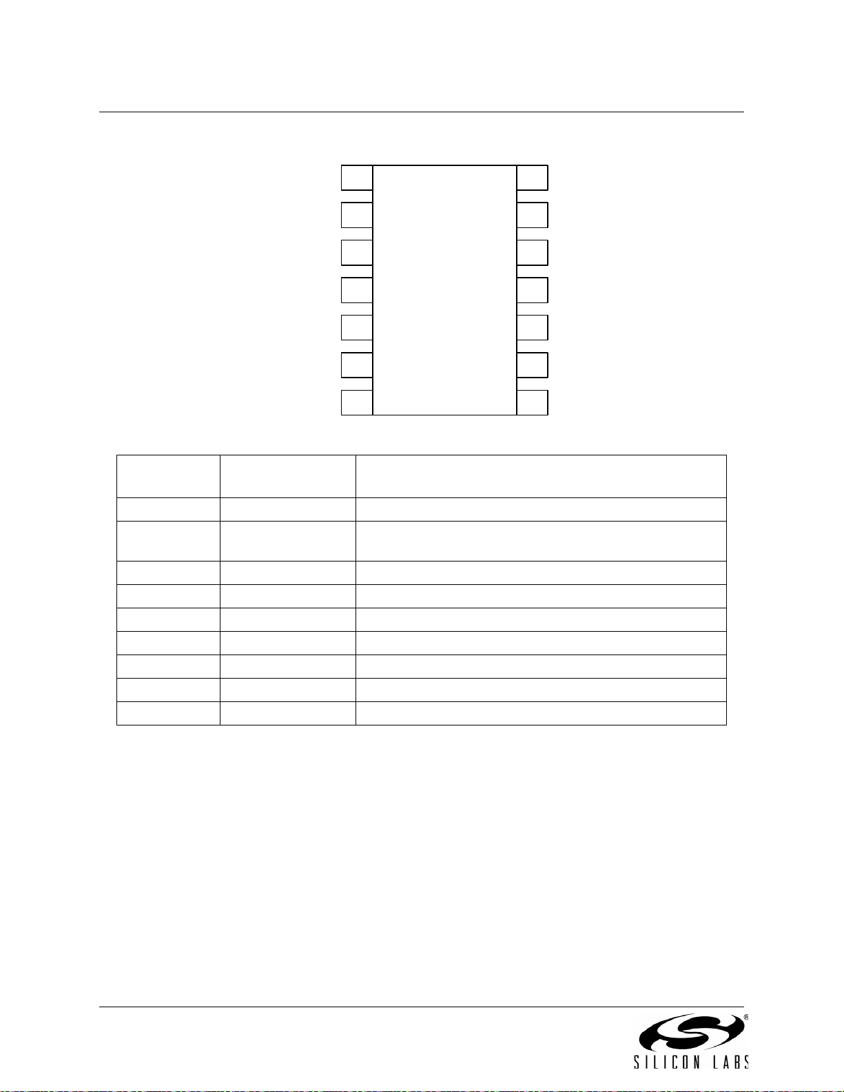
1 10 GPIO1
Si4010-GS
3
4
9
10
11
5
6
12 GPIO2
GPIO3
C2DAT/GPIO4
C2CLK/LEDVDD
VPP/GPIO0/XTAL
TXP
GND
TXM
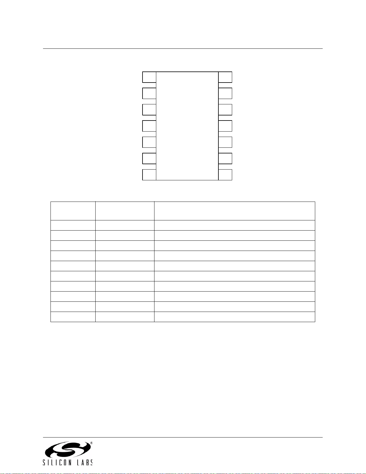
2 13 GPIO1
GPIO9
1 14 GPIO8
87GPIO6GPIO7
14-Pin SOIC
10-Pin MSOP
Features
Si4010-C2
Crystal-less operation
Optional crystal oscillator input
High-Speed 8051 µC Core
Pipeline instruction architecture
70% of instructions in 1 or 2 clocks
Up to 24 MIPs with 24 MHz clock
4 kB RAM/8kB NVM
128 bit EEPROM
256 byte of internal data RAM
12 kB ROM embedded functions
8 byte low leakage RAM
Extensive Digital Peripherals
128 bit AES accelerator
5/9 GPIO with wakeup functionality
LED driver
Data serializer
High-speed frequency counter
On-chip debugging: C2
Unique 4 byte serial number
Ultra low-power sleep timer
Applications
Garage and gate door openers
Remote keyless entry
Description
Single Coin-Cell Battery Operation
Supply voltage: 1.8 to 3.6 V
Standby current < 10 nA
High-performance RF transmitter
Frequency range: 27–960 MHz
+10 dBm output power,
adjustable
Automatic antenna tuning
Symbol rate up to 100 kbps
FSK/OOK modulation
Manchester, NRZ, 4/5 encoder
Analog Peripherals
LDO regulator with POR circuit
Battery voltage monitor
Temperature range –40 to +85 °C
Automotive quality option,
AEC-Q100 (Pending final
qualification testing)
10-pin MSOP/14-pin SOIC
Home automation and security
Wireless remote controls
Ordering Information:
See page 15.
Pin Assignments
The Si4010 is a fully integrated crystal-less CMOS SoC RF transmitter with an
embedded CIP-51 8051 MCU. The device can operate over the –40 to 85
°C
temperature range without requiring an external crystal reference source reducing
board area and BOM cost. The device includes an 8
for programming the user's application along with a 12
kB non volatile memory block
kB ROM of embedded
support code for use in the user's application. The Si4010 includes Silicon
Laboratories' 2-wire C2 Debug and Programming interface, which allows
customers to download their code during the development stage into the on-board
RAM for testing and debug prior to programming the NVM.
The Si4010 is designed for low power battery applications with standby currents of
less than 10
nA to optimize battery life and features automatic wake on button
press support to efficiently move from the standby to active mode state with
minimal customer code support. Built in AES-128 hardware encryption along with
a 128-bit EEPROM can be used to create robust data encryption of the
transmitted packets. A unique 4-byte serial number is programmed into each
device ensuring non-overlapping device identifiers.
The RF transmitter features a high efficiency PA capable of delivering output
power up to +10
algorithm adjusts the antenna tuning at the start of each packet transmission for
optimal output power minimizing the impact of antenna impedance changes due
to the remote being held in a user hand. The devices supports FSK and OOK
dBm and includes an automatic antenna tuning algorithm. This
Patents pending
modulations and includes automatic output power shaping to reduce spectral
spreading and ease regulatory compliance. The output frequency can be adjusted
via software over the entire 27 to 960
adjustable up to a maximum rate of 100
Rev. 1.0 2/11 Copyright © 2011 by Silicon Laboratories Si4010
MHz range. The output data rate is software
kbps.
Si4010-C2
Si4010
NVM
8 Kbyte
EEPROM
128-bit
VDD
GND
PA
RAM/
ROM
PUSH
BUTTONS
CR2032
COIN CELL
1.8 – 3.6 V
DIVIDER
I/O
INTERFACE
GPIO
4/8
INTEGRATED 8051 MCU
LDO REGULATOR
TXM
TXP
LOOP
ANTENNA
FSK OOK
LED
VDD
Functional Block Diagram
2 Rev. 1.0

Si4010-C2
TABLE OF CONTENTS
1. System Overview. . . . . . . . . . . . . . . . . . . . . . . . . . . . . . . . . . . . . . . . . . . . . . . . . . . . . . . . .11
2. Test Circuit. . . . . . . . . . . . . . . . . . . . . . . . . . . . . . . . . . . . . . . . . . . . . . . . . . . . . . . . . . . . . .13
3. Typical Application Schematic . . . . . . . . . . . . . . . . . . . . . . . . . . . . . . . . . . . . . . . . . . . . .14
3.1. Si4010 Used in a 5-Button RKE System with LED Indicator . . . . . . . . . . . . . . . . . . . 14
3.2. Si4010 with an External Crystal in a 4-Button RKE System with LED Indicator . . . .14
4. Ordering Information . . . . . . . . . . . . . . . . . . . . . . . . . . . . . . . . . . . . . . . . . . . . . . . . . . . . .15
5. Top Markings. . . . . . . . . . . . . . . . . . . . . . . . . . . . . . . . . . . . . . . . . . . . . . . . . . . . . . . . . . . .16
5.1. SOIC . . . . . . . . . . . . . . . . . . . . . . . . . . . . . . . . . . . . . . . . . . . . . . . . . . . . . . . . . . . . .16
5.2. MSOP. . . . . . . . . . . . . . . . . . . . . . . . . . . . . . . . . . . . . . . . . . . . . . . . . . . . . . . . . . . . .17
6. Pin Definitions. . . . . . . . . . . . . . . . . . . . . . . . . . . . . . . . . . . . . . . . . . . . . . . . . . . . . . . . . . .18
6.1. MSOP, Application . . . . . . . . . . . . . . . . . . . . . . . . . . . . . . . . . . . . . . . . . . . . . . . . . . .18
6.2. MSOP, Programming/Debug Mode . . . . . . . . . . . . . . . . . . . . . . . . . . . . . . . . . . . . . .19
6.3. SOIC Package, Application . . . . . . . . . . . . . . . . . . . . . . . . . . . . . . . . . . . . . . . . . . . .20
6.4. SOIC Package, Programming/debug Mode. . . . . . . . . . . . . . . . . . . . . . . . . . . . . . . . 21
7. Package Specifications . . . . . . . . . . . . . . . . . . . . . . . . . . . . . . . . . . . . . . . . . . . . . . . . . . .22
7.1. 10-Pin MSOP . . . . . . . . . . . . . . . . . . . . . . . . . . . . . . . . . . . . . . . . . . . . . . . . . . . . . . .22
7.2. 14-pin SOIC Package . . . . . . . . . . . . . . . . . . . . . . . . . . . . . . . . . . . . . . . . . . . . . . . .23
8. PCB Land Pattern 10-Pin MSOP . . . . . . . . . . . . . . . . . . . . . . . . . . . . . . . . . . . . . . . . . . . .24
9. PCB Land Pattern 14-pin SOIC Package. . . . . . . . . . . . . . . . . . . . . . . . . . . . . . . . . . . . . .26
10. Electrical Characteristics . . . . . . . . . . . . . . . . . . . . . . . . . . . . . . . . . . . . . . . . . . . . . . . . .28
11. System Description. . . . . . . . . . . . . . . . . . . . . . . . . . . . . . . . . . . . . . . . . . . . . . . . . . . . . .33
11.1. Overview . . . . . . . . . . . . . . . . . . . . . . . . . . . . . . . . . . . . . . . . . . . . . . . . . . . . . . . . .33
11.2. Setting Basic Si4010 Transmit Parameters . . . . . . . . . . . . . . . . . . . . . . . . . . . . . . .35
11.3. Applications Programming Interface (API) Commands . . . . . . . . . . . . . . . . . . . . . .35
12. Power Amplifier. . . . . . . . . . . . . . . . . . . . . . . . . . . . . . . . . . . . . . . . . . . . . . . . . . . . . . . . .36
12.1. Register Description. . . . . . . . . . . . . . . . . . . . . . . . . . . . . . . . . . . . . . . . . . . . . . . . .38
13. Output Data Serializer (ODS) . . . . . . . . . . . . . . . . . . . . . . . . . . . . . . . . . . . . . . . . . . . . . .40
13.1. Description . . . . . . . . . . . . . . . . . . . . . . . . . . . . . . . . . . . . . . . . . . . . . . . . . . . . . . . .40
13.2. Timing . . . . . . . . . . . . . . . . . . . . . . . . . . . . . . . . . . . . . . . . . . . . . . . . . . . . . . . . . . .40
13.3. Register Description. . . . . . . . . . . . . . . . . . . . . . . . . . . . . . . . . . . . . . . . . . . . . . . . .41
14. LC Oscillator (LCOSC) . . . . . . . . . . . . . . . . . . . . . . . . . . . . . . . . . . . . . . . . . . . . . . . . . . .46
14.1. Register Description. . . . . . . . . . . . . . . . . . . . . . . . . . . . . . . . . . . . . . . . . . . . . . . . .46
15. Low Power Oscillator and System Clock Generator . . . . . . . . . . . . . . . . . . . . . . . . . . .47
15.1. Register Description. . . . . . . . . . . . . . . . . . . . . . . . . . . . . . . . . . . . . . . . . . . . . . . . .47
16. Crystal Oscillator (XO) . . . . . . . . . . . . . . . . . . . . . . . . . . . . . . . . . . . . . . . . . . . . . . . . . . .49
16.1. Register Description. . . . . . . . . . . . . . . . . . . . . . . . . . . . . . . . . . . . . . . . . . . . . . . . .49
17. Frequency Counter . . . . . . . . . . . . . . . . . . . . . . . . . . . . . . . . . . . . . . . . . . . . . . . . . . . . . .50
17.1. Register Description. . . . . . . . . . . . . . . . . . . . . . . . . . . . . . . . . . . . . . . . . . . . . . . . .52
18. Sleep Timer . . . . . . . . . . . . . . . . . . . . . . . . . . . . . . . . . . . . . . . . . . . . . . . . . . . . . . . . . . . .54
19. Bandgap and LDO. . . . . . . . . . . . . . . . . . . . . . . . . . . . . . . . . . . . . . . . . . . . . . . . . . . . . . .54
20. Low Leakage HVRAM . . . . . . . . . . . . . . . . . . . . . . . . . . . . . . . . . . . . . . . . . . . . . . . . . . . .54
21. Temperature Sensor . . . . . . . . . . . . . . . . . . . . . . . . . . . . . . . . . . . . . . . . . . . . . . . . . . . . .54
22. CIP-51 Microcontroller . . . . . . . . . . . . . . . . . . . . . . . . . . . . . . . . . . . . . . . . . . . . . . . . . . .55
3 Rev. 1.0

Si4010-C2
22.1. Instruction Set . . . . . . . . . . . . . . . . . . . . . . . . . . . . . . . . . . . . . . . . . . . . . . . . . . . . . 56
22.1.1. Instruction and CPU Timing................................................................................56
22.2. CIP-51 Register Descriptions. . . . . . . . . . . . . . . . . . . . . . . . . . . . . . . . . . . . . . . . . .61
23. Memory Organization . . . . . . . . . . . . . . . . . . . . . . . . . . . . . . . . . . . . . . . . . . . . . . . . . . . .65
23.1. Program Memory . . . . . . . . . . . . . . . . . . . . . . . . . . . . . . . . . . . . . . . . . . . . . . . . . . .66
23.2. Internal Data Memory. . . . . . . . . . . . . . . . . . . . . . . . . . . . . . . . . . . . . . . . . . . . . . . . 66
23.3. External Data Memory . . . . . . . . . . . . . . . . . . . . . . . . . . . . . . . . . . . . . . . . . . . . . . .66
23.4. General Purpose Registers . . . . . . . . . . . . . . . . . . . . . . . . . . . . . . . . . . . . . . . . . . .66
23.5. Bit Addressable Locations . . . . . . . . . . . . . . . . . . . . . . . . . . . . . . . . . . . . . . . . . . . . 67
23.6. Stack . . . . . . . . . . . . . . . . . . . . . . . . . . . . . . . . . . . . . . . . . . . . . . . . . . . . . . . . . . . . 67
23.7. Special Function Registers (SFR) . . . . . . . . . . . . . . . . . . . . . . . . . . . . . . . . . . . . . .67
23.8. Registers Mapped to XDATA Address Space (XREG) . . . . . . . . . . . . . . . . . . . . . .67
23.9. NVM (OTP) Memory . . . . . . . . . . . . . . . . . . . . . . . . . . . . . . . . . . . . . . . . . . . . . . . .67
23.10. MTP (EEPROM) Memory. . . . . . . . . . . . . . . . . . . . . . . . . . . . . . . . . . . . . . . . . . . . 68
24. System Boot and NVM Programming . . . . . . . . . . . . . . . . . . . . . . . . . . . . . . . . . . . . . . .69
24.1. Startup Overview . . . . . . . . . . . . . . . . . . . . . . . . . . . . . . . . . . . . . . . . . . . . . . . . . . . 69
24.2. Reset . . . . . . . . . . . . . . . . . . . . . . . . . . . . . . . . . . . . . . . . . . . . . . . . . . . . . . . . . . . .70
24.3. Chip Program Levels . . . . . . . . . . . . . . . . . . . . . . . . . . . . . . . . . . . . . . . . . . . . . . . . 70
24.4. NVM Organization . . . . . . . . . . . . . . . . . . . . . . . . . . . . . . . . . . . . . . . . . . . . . . . . . .71
24.5. Device Boot Process . . . . . . . . . . . . . . . . . . . . . . . . . . . . . . . . . . . . . . . . . . . . . . . .72
24.6. Error Handling During Boot . . . . . . . . . . . . . . . . . . . . . . . . . . . . . . . . . . . . . . . . . . .73
24.7. CODE/XDATA RAM Address Map. . . . . . . . . . . . . . . . . . . . . . . . . . . . . . . . . . . . . . 73
24.8. Boot Status Variables. . . . . . . . . . . . . . . . . . . . . . . . . . . . . . . . . . . . . . . . . . . . . . . .76
24.9. Boot Routine Destination Address Space . . . . . . . . . . . . . . . . . . . . . . . . . . . . . . . .79
24.10. NVM Programming. . . . . . . . . . . . . . . . . . . . . . . . . . . . . . . . . . . . . . . . . . . . . . . . . 80
24.11. Retest and Retest Configuration . . . . . . . . . . . . . . . . . . . . . . . . . . . . . . . . . . . . . .81
24.12. Boot and Retest Protection NVM Control Byte . . . . . . . . . . . . . . . . . . . . . . . . . . .83
24.13. Chip Protection Control Register . . . . . . . . . . . . . . . . . . . . . . . . . . . . . . . . . . . . . . 84
25. On-Chip Registers. . . . . . . . . . . . . . . . . . . . . . . . . . . . . . . . . . . . . . . . . . . . . . . . . . . . . . .85
25.1. Special Function Registers . . . . . . . . . . . . . . . . . . . . . . . . . . . . . . . . . . . . . . . . . . .85
25.2. XREG Registers. . . . . . . . . . . . . . . . . . . . . . . . . . . . . . . . . . . . . . . . . . . . . . . . . . . .88
26. Interrupts . . . . . . . . . . . . . . . . . . . . . . . . . . . . . . . . . . . . . . . . . . . . . . . . . . . . . . . . . . . . . .91
26.1. MCU Interrupt Sources and Vectors . . . . . . . . . . . . . . . . . . . . . . . . . . . . . . . . . . . .92
26.2. Interrupt Priorities. . . . . . . . . . . . . . . . . . . . . . . . . . . . . . . . . . . . . . . . . . . . . . . . . . .92
26.3. Interrupt Latency . . . . . . . . . . . . . . . . . . . . . . . . . . . . . . . . . . . . . . . . . . . . . . . . . . . 92
26.4. Interrupt Register Descriptions. . . . . . . . . . . . . . . . . . . . . . . . . . . . . . . . . . . . . . . . . 93
26.5. External Interrupts . . . . . . . . . . . . . . . . . . . . . . . . . . . . . . . . . . . . . . . . . . . . . . . . . .99
27. Power Management Modes . . . . . . . . . . . . . . . . . . . . . . . . . . . . . . . . . . . . . . . . . . . . . .101
27.1. Idle Mode . . . . . . . . . . . . . . . . . . . . . . . . . . . . . . . . . . . . . . . . . . . . . . . . . . . . . . . . 101
27.2. Stop Mode . . . . . . . . . . . . . . . . . . . . . . . . . . . . . . . . . . . . . . . . . . . . . . . . . . . . . . .101
28. AES Hardware Accelerator. . . . . . . . . . . . . . . . . . . . . . . . . . . . . . . . . . . . . . . . . . . . . . .103
28.1. AES SFR Registers . . . . . . . . . . . . . . . . . . . . . . . . . . . . . . . . . . . . . . . . . . . . . . . . 103
29. Reset Sources . . . . . . . . . . . . . . . . . . . . . . . . . . . . . . . . . . . . . . . . . . . . . . . . . . . . . . . . .106
29.1. Device Boot Outline . . . . . . . . . . . . . . . . . . . . . . . . . . . . . . . . . . . . . . . . . . . . . . . .106
29.2. External Reset . . . . . . . . . . . . . . . . . . . . . . . . . . . . . . . . . . . . . . . . . . . . . . . . . . . .106
29.3. Software Reset. . . . . . . . . . . . . . . . . . . . . . . . . . . . . . . . . . . . . . . . . . . . . . . . . . . .107
4 Rev. 1.0

Si4010-C2
30. Port Input/Output. . . . . . . . . . . . . . . . . . . . . . . . . . . . . . . . . . . . . . . . . . . . . . . . . . . . . . .108
30.1. GPIO Pin Special Roles . . . . . . . . . . . . . . . . . . . . . . . . . . . . . . . . . . . . . . . . . . . . .111
30.2. Pullup Roff Option . . . . . . . . . . . . . . . . . . . . . . . . . . . . . . . . . . . . . . . . . . . . . . . . .112
30.3. Matrix Mode Option . . . . . . . . . . . . . . . . . . . . . . . . . . . . . . . . . . . . . . . . . . . . . . . .112
30.4. Pullup Roff and Matrix Mode Option Control . . . . . . . . . . . . . . . . . . . . . . . . . . . . . 114
30.5. Special GPIO Modes Control . . . . . . . . . . . . . . . . . . . . . . . . . . . . . . . . . . . . . . . . .115
30.6. LED Driver on GPIO[5]. . . . . . . . . . . . . . . . . . . . . . . . . . . . . . . . . . . . . . . . . . . . . .117
31. Clock Output Generation . . . . . . . . . . . . . . . . . . . . . . . . . . . . . . . . . . . . . . . . . . . . . . . .123
31.1. Register Description. . . . . . . . . . . . . . . . . . . . . . . . . . . . . . . . . . . . . . . . . . . . . . . .124
32. Control and System Setting Registers . . . . . . . . . . . . . . . . . . . . . . . . . . . . . . . . . . . . .126
33. Real Time Clock Timer . . . . . . . . . . . . . . . . . . . . . . . . . . . . . . . . . . . . . . . . . . . . . . . . . .128
33.1. RTC Interrupt Flag Time Uniformity . . . . . . . . . . . . . . . . . . . . . . . . . . . . . . . . . . . . 129
33.2. Register Description. . . . . . . . . . . . . . . . . . . . . . . . . . . . . . . . . . . . . . . . . . . . . . . .129
34. Timers 2 and 3. . . . . . . . . . . . . . . . . . . . . . . . . . . . . . . . . . . . . . . . . . . . . . . . . . . . . . . . .131
34.1. Interrupt Flag Generation . . . . . . . . . . . . . . . . . . . . . . . . . . . . . . . . . . . . . . . . . . . .132
34.2. 16-bit Timer with Auto Reload (Wide Mode) . . . . . . . . . . . . . . . . . . . . . . . . . . . . .133
34.3. 16-bit Capture Mode (Wide Mode). . . . . . . . . . . . . . . . . . . . . . . . . . . . . . . . . . . . .133
34.4. 8-Bit Timer/Timer Mode (Split Mode) . . . . . . . . . . . . . . . . . . . . . . . . . . . . . . . . . . .134
34.5. 8-Bit Capture/Capture Mode (Split Mode) . . . . . . . . . . . . . . . . . . . . . . . . . . . . . . . 135
34.6. 8-Bit Timer/Capture Mode (Split Mode) . . . . . . . . . . . . . . . . . . . . . . . . . . . . . . . . .136
35. C2 Interface . . . . . . . . . . . . . . . . . . . . . . . . . . . . . . . . . . . . . . . . . . . . . . . . . . . . . . . . . . .148
35.1. C2 Pin Sharing . . . . . . . . . . . . . . . . . . . . . . . . . . . . . . . . . . . . . . . . . . . . . . . . . . . .148
36. IDE Development Environment and Debugging Chain . . . . . . . . . . . . . . . . . . . . . . . .151
36.1. Functionality Limitations While Using IDE Development Environment . . . . . . . . .151
36.2. Chip Shutdown Limitation . . . . . . . . . . . . . . . . . . . . . . . . . . . . . . . . . . . . . . . . . . .152
36.3. LED Driver Usage while Using IDE Debugging Chain . . . . . . . . . . . . . . . . . . . . . .152
37. Additional Reference Resources. . . . . . . . . . . . . . . . . . . . . . . . . . . . . . . . . . . . . . . . . .154
Document Change List. . . . . . . . . . . . . . . . . . . . . . . . . . . . . . . . . . . . . . . . . . . . . . . . . . . . .155
Contact Information . . . . . . . . . . . . . . . . . . . . . . . . . . . . . . . . . . . . . . . . . . . . . . . . . . . . . . .156
Rev. 1.0 5

Si4010-C2
LIST OF FIGURES
Figure 1.1. Si4010 Block Diagram ............................................................................................12
Figure 2.1. Test Block Diagram with 10-Pin MSOP ................................................................. 13
Figure 3.1. Si4010 Used in a 5-button RKE System with LED Indicator ..................................14
Figure 3.2. Si4010 with an External Crystal in a 4-button RKE System with LED Indicator ..... 14
Figure 1. Si4010 Top Marking ..................................................................................................16
Figure 2. Si4010 Top Marking ..................................................................................................17
Figure 7.1. 10-Pin MSOP Package ..........................................................................................22
Figure 7.2. 14-Pin SOIC Package ............................................................................................23
Figure 8.1. 10-Pin MSOP Recommended PCB Land Pattern ..................................................24
Figure 9.1. 14-Pin SOIC Recommended PCB Land Pattern ....................................................26
Figure 11.1. Functional Block Diagram ....................................................................................33
Figure 12.1. Simplified PA Block Diagram ...............................................................................36
Figure 13.1. OOK Timing Example ..........................................................................................40
Figure 13.2. FSK Timing Example ...........................................................................................40
Figure 17.1. Frequency Counter Block Diagram ......................................................................50
Figure 22.1. CIP-51 Block Diagram ..........................................................................................55
Figure 23.1. Address Space Map after the Boot ......................................................................65
Figure 24.1. NVM Address Map ...............................................................................................72
Figure 24.2. CODE/XDATA RAM Address Map .......................................................................75
Figure 24.3. Boot Routine Destination CPU Address Space for Copy from NVM ....................79
Figure 30.1. Device Package and Port Assignments .............................................................108
Figure 30.2. GPIO[3:1] Functional Diagram ...........................................................................110
Figure 30.3. Other GPIO Functional Diagram ........................................................................110
Figure 30.4. Push Button Organization in Matrix Mode ..........................................................113
Figure 30.5. GPIO[5] LED Driver Block Diagram ...................................................................117
Figure 31.1. Output Clock Generator Block Diagram .............................................................123
Figure 33.1. RTC Timer Block Diagram .................................................................................128
Figure 34.1. Timer Interrupt Generation .................................................................................132
Figure 34.2. Timer 16-bit Mode Block Diagram (Wide Mode) ................................................133
Figure 34.3. Capture 16-bit Mode Block Diagram (Wide Mode) ............................................134
Figure 34.4. Two 8-bit Timers in Timer/Timer Configuration (Split Mode) .............................135
Figure 34.5. Two 8-bit Timers in Capture/Capture Configuration (Split Mode) ...................... 136
Figure 34.6. Two 8-Bit TImers in Timer/Capture Configuration (Split Mode) ......................... 137
Figure 34.7. Two 8-Bit Timers In Capture/Timer Configuration (Split Mode) ......................... 138
Figure 35.1. 10-pin C2 USB Debugging Adapter Connection to Device ................................148
Figure 35.2. 14-Pin C2 ToolStick Connection to Device ........................................................150
6 Rev. 1.0

Si4010-C2
LIST OF TABLES
Table 4.1. Product Selection Guide ..........................................................................................15
Table 1. Top Marking Explanation ............................................................................................16
Table 2. Top Marking Explanation ............................................................................................17
Table 7.1. Package Dimensions ...............................................................................................22
Table 7.2. Package Dimensions ...............................................................................................23
Table 8.1. 10-Pin MSOP Dimensions ....................................................................................... 25
Table 9.1. PCB Land Pattern Dimensions ................................................................................27
Table 10.1. Recommended Operating Conditions ...................................................................28
Table 10.2. Absolute Maximum Ratings
Table 10.3. DC Characteristics ................................................................................................29
Table 10.4. Si4010 RF Transmitter Characteristics .................................................................30
Table 10.5. Low Battery Detector Characteristics ....................................................................31
Table 10.6. Optional Crystal Oscillator Characteristics ............................................................31
Table 10.7. EEPROM Characteristics ......................................................................................32
Table 10.8. Low Power Oscillator Characteristics ....................................................................32
Table 10.9. Sleep Timer Characteristics ..................................................................................32
Table 22.1. CIP-51 Instruction Set Summary ...........................................................................57
Table 24.1. Boot XDATA Status Variables ...............................................................................76
Table 24.2. Run Chip Retest Protection Flags: NVM Programmer .......................................... 81
Table 25.1. Special Function Register (SFR) Memory Map .....................................................85
Table 25.2. Special Function Registers ....................................................................................86
Table 25.3. XREG Register Memory Map in External Memory ................................................89
Table 25.4. XREG Registers ....................................................................................................90
Table 26.1. Interrupt Summary .................................................................................................93
Table 30.1. 10–Pin Mode .......................................................................................................109
Table 30.2. 14–Pin Mode .......................................................................................................109
Table 30.3. GPIO Special Roles ............................................................................................111
Table 30.4. GPIO Special Roles Control and Order ...............................................................116
1,2
..............................................................................28
Rev. 1.0 7

Si4010-C2
LIST OF XREG REGISTERS
XREG Definition 12.2. wPA_CAP .......................................................................................... 38
XREG Definition 12.3. bPA_TRIM .......................................................................................... 39
XREG Definition 15.1. bLPOSC_TRIM .................................................................................. 47
XREG Definition 16.1. bXO_CTRL ......................................................................................... 49
XREG Definition 17.3. IFC_COUNT ....................................................................................... 53
XREG Definition 23.1. abMTP_RDATA[16] ........................................................................... 68
8 Rev. 1.0

Si4010-C2
LIST OF SFR REGISTERS
SFR Definition 12.1. PA_LVL ...................................................................................................38
SFR Definition 13.1. ODS_CTRL .............................................................................................41
SFR Definition 13.2. ODS_TIMING ..........................................................................................42
SFR Definition 13.3. ODS_DATA .............................................................................................43
SFR Definition 13.4. ODS_RATEL ...........................................................................................43
SFR Definition 13.5. ODS_RATEH ..........................................................................................44
SFR Definition 13.6. ODS_WARM1 .........................................................................................44
SFR Definition 13.7. ODS_WARM2 .........................................................................................45
SFR Definition 14.1. LC_FSK ...................................................................................................46
SFR Definition 15.2. SYSGEN .................................................................................................48
SFR Definition 17.1. FC_CTRL ................................................................................................52
SFR Definition 17.2. FC_INTERVAL ........................................................................................53
SFR Definition 22.1. DPL .........................................................................................................61
SFR Definition 22.2. DPH ......................................................................................................
SFR Definition 22.3. SP ...........................................................................................................62
SFR Definition 22.4. ACC .........................................................................................................62
SFR Definition 22.5. B .............................................................................................................. 63
SFR Definition 22.6. PSW ........................................................................................................64
SFR Definition 24.2. BOOT_FLAGS ........................................................................................78
NVM Byte Definition 24.3. PROT3_CTRL ................................................................................83
SFR Definition 24.4. PROT0_CTRL ......................................................................................... 84
SFR Definition 26.1. IE ............................................................................................................. 94
SFR Definition 26.2. IP ............................................................................................................. 95
SFR Definition 26.3. EIE1 ........................................................................................................96
SFR Definition 26.4. EIP1 ........................................................................................................97
SFR Definition 26.5. INT_FLAGS .............................................................................................98
SFR Definition 26.6. PORT_INTCFG ..................................................................................... 100
SFR Definition 27.1. PCON ....................................................................................................1
SFR Definition 28.1. GFM_DATA ...........................................................................................104
SFR Definition 28.2. GFM_CONST ........................................................................................104
SFR Definition 28.3. SBOX_DATA .........................................................................................105
SFR Definition 28.4. SYS_SET ..............................................................................................105
SFR Definition 30.1. P0 ..........................................................................................................118
SFR Definition 30.2. P0CON .................................................................................................. 119
SFR Definition 30.3. P1 ..........................................................................................................119
SFR Definition 30.4. P1CON .................................................................................................. 120
SFR Definition 30.5. P2 ..........................................................................................................120
SFR Definition 30.6. PORT_CTRL .........................................................................................121
SFR Definition 30.7. PORT_SET ...........................................................................................122
SFR Definition 31.1. CLKOUT_SET .......................................................................................124
SFR Definition 32.1. GPR_CTRL ...........................................................................................126
SFR Definition 32.2. GPR_DATA ...........................................................................................126
SFR Definition 32.3. RBIT_DATA ..........................................................................................127
...61
02
9 Rev. 1.0

Si4010-C2
SFR Definition 33.1. RTC_CTRL ...........................................................................................130
SFR Definition 34.1. TMR_CLKSEL .......................................................................................139
SFR Definition 34.2. TMR2CTRL ...........................................................................................140
SFR Definition 34.3. TMR2RL ................................................................................................ 142
SFR Definition 34.4. TMR2RH ...............................................................................................142
SFR Definition 34.5. TMR2L ..................................................................................................143
SFR Definition 34.6. TMR2H .................................................................................................. 143
SFR Definition 34.7. TMR3CTRL ...........................................................................................144
SFR Definition 34.8. TMR3RL ................................................................................................ 146
SFR Definition 34.9. TMR3RH ...............................................................................................146
SFR Definition 34.10. TMR3L ................................................................................................147
SFR Definition 34.11. TMR3H ................................................................................................ 147
10 Rev. 1.0

Si4010-C2
1. System Overview
The Si4010 is a fully integrated crystal-less CMOS SoC RF transmitter with an embedded CIP-51 8051
MCU designed for the sub 1 GHz ISM frequency bands. This chip is optimized for battery powered applications with operating voltages from 1.8 to 3.6 V and ultra-low current consumption with a standby current of
less than 10 nA. The high power amplifier can supply up to +10 dBm output power with 19.5 dB of programmable range. Moreover, the SoC transmitter includes a patented antenna tuning circuit that automatically fine tunes the resonance frequency and impedance matching between the PA output and the
connected antenna for optimum transmit efficiency and low harmonic content. FSK and OOK modulation is
supported with symbol rates up to 100 kbps. Like all wireless devices, users are responsible for complying
with applicable local regulatory requirements for radio transmissions.
The embedded CIP-51 8051 MCU provides the core functionality of the Si4010. User software has complete control of all peripherals, and may individually shut down any or all peripherals for power savings. A
space of 8 kB of on-chip one-time programmable NVM memory is available to store the user program and
can also store unique transmit IDs. In case of power outages due to battery removal, 128 bits of EEPROM
is available for counter or other operations providing non-volatile storage capability. A library of useful software functions such as AES encryption, a patented 32-bit counter providing 1 M cycles of read/write
endurance, and many other functions are included in the 12 kB of ROM to reduce user design time and
code space. General purpose input/output pins with push button wake-on touch capability, a programmable system clock, and ultra low power timers are also available to further reduce current consumption.
The Si4010 includes Silicon Laboratories' 2-wire C2 Debug and Programming interface. This debug logic
supports memory inspection, viewing and modification of special function registers (SFR), setting break
points, single stepping, and run and halt commands. All analog and digital peripherals are fully functional
while debugging using C2. The two C2 interface pins can be shared with user functions, allowing in-system
debugging without occupying package pins.
The device leverages Silicon Labs' patented and proven crystal-less oscillator technology and offers better
than ±150 ppm carrier frequency stability over the temperature range of 0 to + 70 °C and ±250 ppm carrier
frequency stability over the industrial range of –40 to + 85 °C without the use of an external crystal or frequency reference. The internal MCU automatically calibrates the on-chip voltage controlled oscillator
(LCOSC) which forms the output carrier frequency for process and temperature variations. An external 1pin crystal oscillator option is available for applications requiring tighter frequency tolerances.
Digital integration reduces the amount of required external components compared to traditional offerings,
resulting in a solution that only requires a printed circuit board (PCB) implementation area of approximately
25 by 50 mm (including battery, switches, and 25 mm
improves the system manufacturing reliability and quality and minimizes costs. This chip offers industry
leading RF performance, high integration, flexibility, low BOM, small board area, and ease of design. No
production alignment is necessary as all RF functions are integrated into the device.
2
antenna). The high integration of the Si4010
Rev. 1.0 11
Si4010-C2
Si4010
SFR
BUS
C2
PORT
CONTR
TEMP
DEMOD
ODS
FREQ
COUNTER
CIP-51 8051
CONTROLLER CORE
256 BYTE IRAM
256 BYTE XREG
4K BYTE RAM
12K BYTE ROM
DIGITAL PERIPHERALS
INTC
RTC
TMR 2,3
AES 128b ACCEL
GPIO0/XTAL/VPP
GPIO1
GPIO2
GPIO3
GPIO4/C2DAT
GPIO5/C2CLK/LED
GPIO6
GPIO7
GPIO8
GPIO9
NVM
8 KB
EEPROM
128-bit
MEMORY
CONTROLLER
14P SOIC
Package
Only
LCOSC
PADIVIDER
XTAL
OSC
HVRAM
8 Byte
AUTO
TUNE
FSK
OOK
LPOSC
TEMP
SENSOR
LDO
POR
BANDGAP
VA
VD
TXP
TXM
VDD
GND
SLP
TMR
RF ANALOG CORE
12 Rev. 1.0
Figure 1.1. Si4010 Block Diagram

2. Test Circuit
U1
Si4010-GT
GPIO0
GND
TXM
TXP
VDD
GPIO1
GPIO2
GPIO3
GPIO4
LED
1
2
3
4
5
10
9
8
7
6
C1
1 uF
TESTER
INTERFACE
GP1
GP2
GP3
GP4
GP5
TEST
EQUIPMENT
GP0
VDD
MATCHING
NETWORK
Si4010-C2
Figure 2.1. Test Block Diagram with 10-Pin MSOP
Rev. 1.0 13
Si4010-C2
U1
Si4010-GT
GPI0
GND
TXM
TXP
VDD
GPIO1
GPIO2
GPIO3
GPIO4
LED
1
2
3
4
5
10
9
8
7
6
CR2032
COIN CELL
1.8 to 3.6 V
LOOP
A
A
C1
1uF
SW1
D1
SW0
SW2
SW3
SW4
C2
U1
Si4010-GT
GPI0
GND
TXM
TXP
VDD
GPIO1
GPIO2
GPIO3
GPIO4
LED
1
2
3
4
5
10
9
8
7
6
CR2032
COIN CELL
1.8 to 3.6 V
LOOP
ANTENNA
C1
1uF
SW1
D1
SW2
SW3
SW4
C2
X1
C3
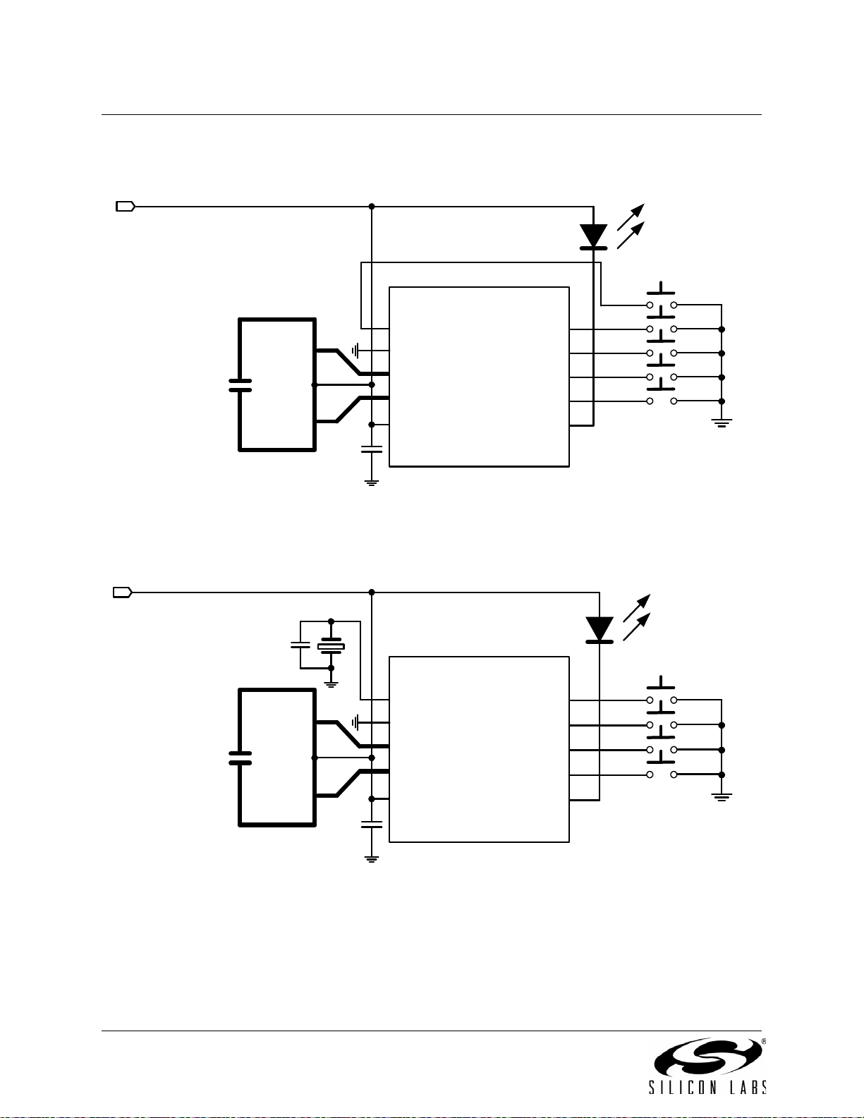
3. Typical Application Schematic
3.1. Si4010 Used in a 5-Button RKE System with LED Indicator
NTENN
Figure 3.1. Si4010 Used in a 5-button RKE System with LED Indicator
3.2. Si4010 with an External Crystal in a 4-Button RKE System with LED Indicator
Figure 3.2. Si4010 with an External Crystal in a 4-button RKE System with LED Indicator
14 Rev. 1.0
4. Ordering Information
Table 4.1. Product Selection Guide
Si4010-C2
3
Ordering Part Number1MIPS (Peak)
Si4010-C2-GT 24 8k 4k Y 256 8 128 Y 5 1YYYY— Y
Si4010-C2-GS 24 8k 4k Y 256 8 128 Y 9 1YYYY— Y
Si4010-C2-AT 24 8k 4k Y 256 8 128 Y 5 1YYYYY Y
Si4010-C2-AS 24 8k 4k Y 256 8 128 Y 9 1YYYYY Y
Notes:
1. Add an “(R)” at the end of the device part number to denote tape and reel option.
2. Assumes LED driver is used and no external crystal.
3. AEC Q100 qualification is pending.
NVM (OTP) Memory (Bytes)
RAM (Bytes)
Embedded ROM Functions
Internal Data RAM (Bytes)
HVRAM (Bytes)
EEPROM (Bits)
128-Bit AES Accelerator
GPIO with Wakeup2LED Driver
Sleep Timer
+10 dBm RF Transmitter
LDO with POR Circuit
Low Battery Detector
Automotive Qualified
Lead-free (RoHS Compliant)
MSOP-10
SOIC-14
MSOP-10
SOIC-14
Package
Rev. 1.0 15
Si4010-C2
5. Top Markings
5.1. SOIC
Figure 1. Si4010 Top Marking
Table 1. Top Marking Explanation
Line Characters Description
Line 1
Line 2
Circle = 1.1 mm Diameter
Left-Justified
Customer Part Number
YY = Year
WW = Work Week
TTTTTT = Trace Code
"e3" Pb-Free Symbol
Si4010C2
Assigned by the Assembly House. Corresponds to the year and
work week of the assembly date.
Manufacturing code characters from the Markings section of the
Assembly Purchase Order form.
16 Rev. 1.0

5.2. MSOP
Si4010-C2
Figure 2. Si4010 Top Marking
Table 2. Top Marking Explanation
Line Characters Description
Line 1 Device Part Number
Line 2 TTTT = Trace Code
Line 3 YWW = Date Code
10C2
Line 2 from the "Markings" section of the Assembly Purchase
Order form.
Date Code assigned by the assembly house.
Y = Last Digit of Current Year (Ex: 2008 = 8)
WW = Work Week of Mold Date.
Rev. 1.0 17
Si4010-C2
GPIO0/XTAL
Si4010-GT
2
3
6
7
8
4
5
9GPIO2
GPIO3
GPIO4
LEDVDD
TXP
GND
TXM
1 10 GPIO1
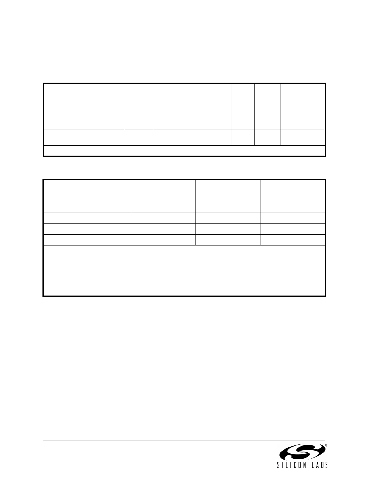
6. Pin Definitions
6.1. MSOP, Application
Pin Number(s) Name Description
1
2
3, 4
5
6
7, 8, 9, 10
GPIO0/XTAL General purpose input pin.
Can be configured as an input pin for a crystal.
GND Ground. Connect to ground plane on PCB.
TXM, TXP Transmitter differential outputs.
VDD Power.
LED Dedicated LED driver.
GPIO[4:1] General purpose input/output pins.
18 Rev. 1.0
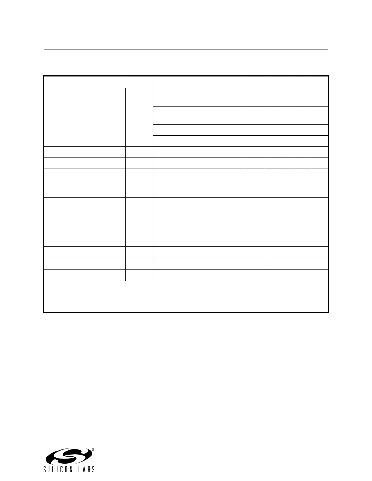
6.2. MSOP, Programming/Debug Mode
VPP/GPIO0/XTAL
Si4010-GT
2
3
6
7
8
4
5
9GPIO2
GPIO3
C2DAT/GPIO4
C2CLK/LEDVDD
TXP
GND
TXM
1 10 GPIO1
Pin Number(s) Name Description
Si4010-C2
1 VPP
2GND
3TXM
4TXP
5VDD
6 C2CLK
7C2DAT
8, 9, 10 GPIO[3:1]
+6.5 V required for NVM (OTP) Memory programming.
Ground. Connect to ground plane on PCB.
Transmitter differential output.
Transmitter differential output.
Power.
C2 clock interface.
C2 data input/output pin.
General purpose input/output pins.
Rev. 1.0 19
Si4010-C2
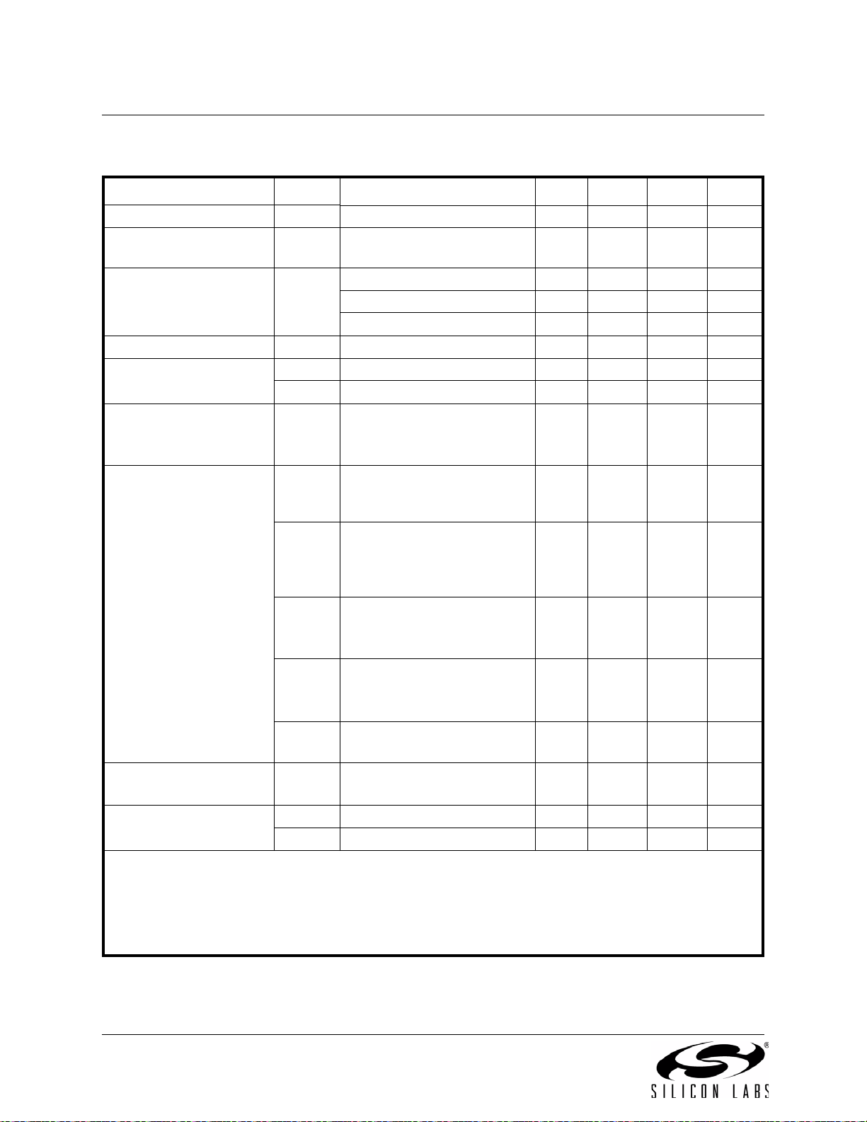
Si4010-GS
3
4
9
10
11
5
6
12 GPIO2
GPIO3
GPIO4
LEDVDD
GPIO0/XTAL
TXP
GND
TXM
2 13 GPIO1
GPIO9
1 14 GPIO8
87GPIO6GPIO7
6.3. SOIC Package, Application
Pin
Number(s)
1 GPIO9 General purpose input/output pin
2 GPIO0/XTAL General purpose input pin. Can be configured as an input
3 GND Ground. Connect to ground plane on PCB
4,5 TXM, TXP Transmitter differential outputs
6VDDPower
7,8 GPIO[7:6] General purpose input/output pins
9 LED Dedicated LED driver
10,11,12,13 GPIO[4:1] General purpose input/output pins
14 GPIO8 General purpose input/output pin
Name Description
pin for a crystal
20 Rev. 1.0
6.4. SOIC Package, Programming/debug Mode
Si4010-GS
3
4
9
10
11
5
6
12 GPIO2
GPIO3
C2DAT/GPIO4
C2CLK/LEDVDD
VPP/GPIO0/XTAL
TXP
GND
TXM
2 13 GPIO1
GPIO9
1 14 GPIO8
87GPIO6GPIO7
Si4010-C2
Pin
Number(s)
1 GPIO9 General purpose input/output pin
2 VPP +6.5 V required for NVM (OTP) Memory programming
3 GND Ground. Connect to ground plane on PCB
4,5 TXM, TXP Transmitter differential outputs
6VDDPower
7,8 GPIO[7:6] General purpose input/output pins
9 C2CLK C2 clock interface
10 C2DAT C2 data input/output pin
11,12,13 GPIO[4:1] General purpose input/output pins
14 GPIO8 General purpose input/output pin
Name Description
Rev. 1.0 21
Si4010-C2
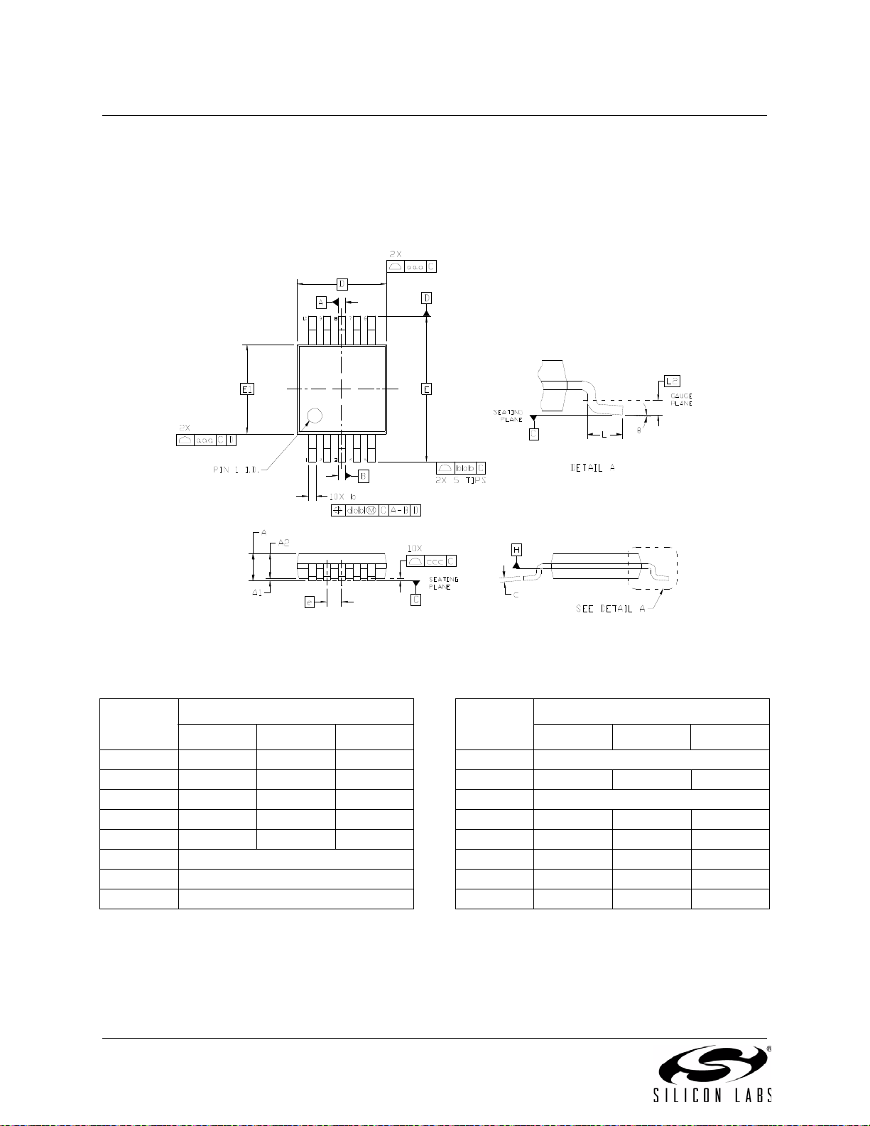
7. Package Specifications
7.1. 10-Pin MSOP
Figure 7.1 illustrates the package details for the Si4010, 10-pin MSOP package. Table 7.1 lists the values
for the dimensions shown in the illustration.
Figure 7.1. 10-Pin MSOP Package
Table 7.1. Package Dimensions
Symbol Millimeters Symbol Millimeters
Min Nom Max Min Nom Max
A — — 1.10 e 0.50 BSC
A1 0.00 — 0.15 L 0.40 0.60 0.80
A2 0.75 0.85 0.95 L2 0.25 BSC
b 0.17 — 0.33 q 0° — 8°
c 0.08 — 0.23 aaa — — 0.20
D 3.00 BSC bbb — — 0.25
E 4.90 BSC ccc — — 0.10
E1 3.00 BSC ddd — — 0.08
Notes:
1. All dimensions are shown in millimeters (mm).
2. Dimensioning and tolerancing per ASME Y14.5M-1994.
3. This drawing conforms to JEDEC Outline MO-187, Variation “BA.”
4. Recommended card reflow profile is per the JEDEC/IPC J-STD-020 specification for Small Body Components.
22 Rev. 1.0
Si4010-C2
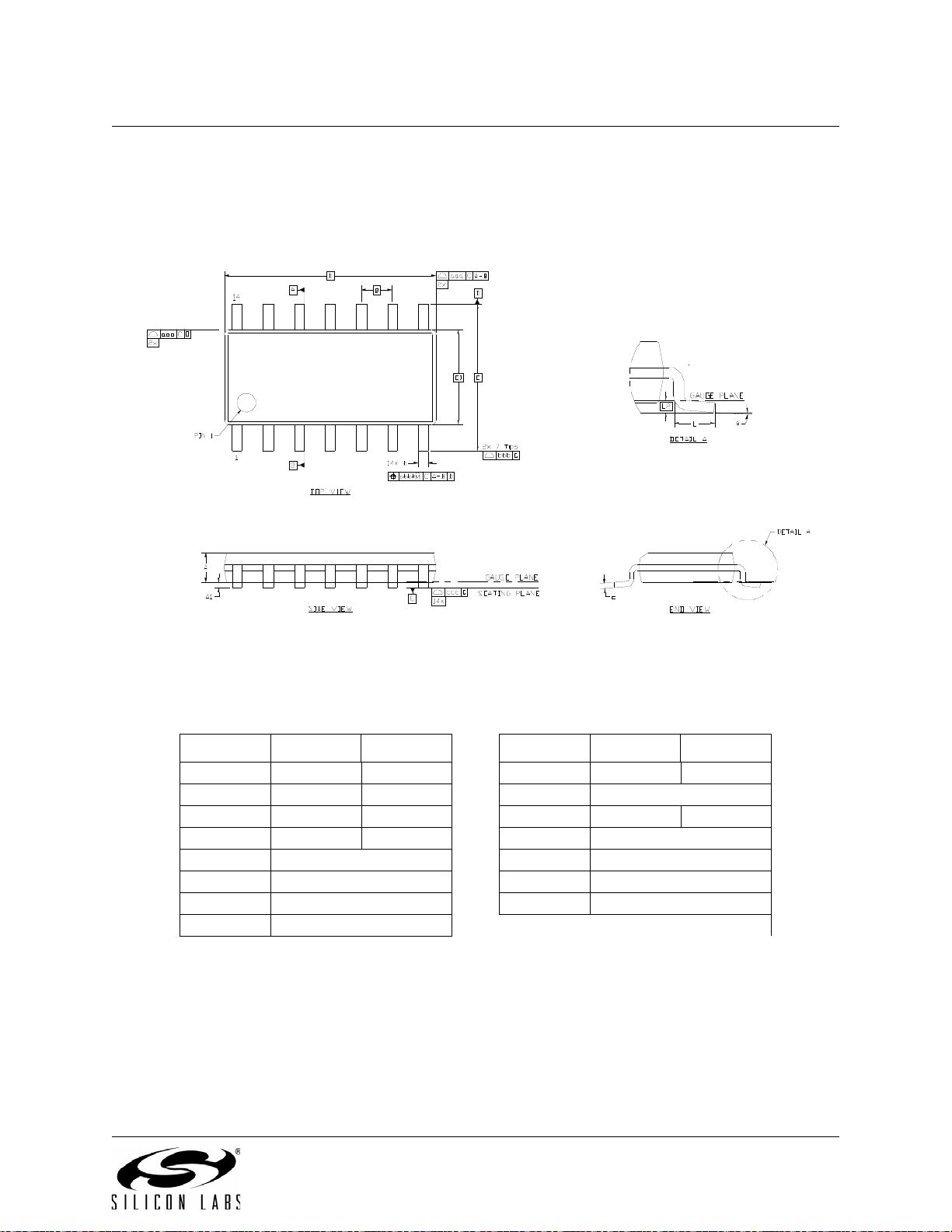
7.2. 14-pin SOIC Package
Figure 7.2 illustrates the package details for the Si4010, 14-pin SOIC package. Table 7.2 lists the values
for the dimensions shown in the illustration.
Figure 7.2. 14-Pin SOIC Package
Table 7.2. Package Dimensions
Symbol Min Max Symbol Min Max
A — 1.75 L 0.40 1.27
A1 0.10 0.25 L2 0.25 BSC
b 0.33 0.51 Q 0° 8°
c 0.17 0.25 aaa 0.10
D 8.65 BSC bbb 0.20
E 6.00 BSC ccc 0.10
E1 3.90 BSC ddd 0.25
e 1.27 BSC
Notes:
1. All dimensions are shown in millimeters (mm).
2. Dimensioning and tolerancing per ASME Y14.5M-1994.
3. This drawing conforms to JEDEC Outline MS012, variation AB.”
4. Recommended card reflow profile is per the JEDEC/IPC J-STD-020 specification for
Small Body Components.
Rev. 1.0 23
Si4010-C2
8. PCB Land Pattern 10-Pin MSOP
Figure 8.1. 10-Pin MSOP Recommended PCB Land Pattern
24 Rev. 1.0
Table 8.1. 10-Pin MSOP Dimensions
Dimension MIN MAX
C1 4.40 REF
E 0.50 BSC
G1 3.00 —
X1 — 0.30
Y1 1.40 REF
Z1 — 5.80
Notes:
General
1. All dimensions shown are in millimeters (mm) unless otherwise noted.
2. Dimensioning and Tolerancing per ASME Y14.5M-1994.
3. This Land Pattern Design is based on the IPC-7351 guidelines.
4. All dimensions shown are at Maximum Material Condition (MMC).
Least Material Condition (LMC) is calculated based on a Fabrication
Allowance of 0.05mm.
Solder Mask Design
1. All metal pads are to be non-solder mask defined (NSMD). Clearance
between the solder mask and the metal pad is to be 60 m minimum, all
the way around the pad.
Stencil Design
1. A stainless steel, laser-cut and electro-polished stencil with
trapezoidal walls should be used to assure good solder paste release.
2. The stencil thickness should be 0.125mm (5 mils).
3. The ratio of stencil aperture to land pad size should be 1:1.
Card Assembly
1. A No-Clean, Type-3 solder paste is recommended.
2. The recommended card reflow profile is per the JEDEC/IPC J-STD-
020 specification for Small Body Components.
Si4010-C2
Rev. 1.0 25
Si4010-C2
9. PCB Land Pattern 14-pin SOIC Package
Figure 9.1. 14-Pin SOIC Recommended PCB Land Pattern
26 Rev. 1.0
Table 9.1. PCB Land Pattern Dimensions
Dimension MIN MAX
C1 5.30 5.40
E 1.27 BSC
X1 0.50 0.60
Y1 1.45 1.55
Notes:
General
1. All dimensions shown are in millimeters (mm) unless otherwise noted.
2. This land pattern design is based on the IPC-7351 guidelines.
Solder Mask Design
1. All metal pads are to be non-solder mask defined (NSMD). Clearance
between the solder mask and the metal pad is to be 60 µm minimum,
all the way around the pad.
Si4010-C2
Stencil Design
1. A stainless steel, laser-cut and electro-polished stencil with
trapezoidal walls should be used to assure good solder paste release.
2. The stencil thickness should be 0.125 mm (5 mils).
3. The ratio of stencil aperture to land pad size should be 1:1 for all
perimeter pads.
Card Assembly
1. A No-Clean, Type-3 solder paste is recommended.
2. The recommended card reflow profile is per the JEDEC/IPC J-STD-
020 specification for Small Body Components.
Rev. 1.0 27
Si4010-C2
10. Electrical Characteristics
Table 10.1. Recommended Operating Conditions
Parameter Symbol Test Condition Min Typ Max Unit
Supply Voltage V
DD
Supply Voltage Slew Rate Initial Battery Insertion* 20 — 650 mV/
Ambient Temperature T
–40 25 85 °C
A
Digital Input Range Digital Input Signals –0.3 — V
*Note: Recommend bypass capacitor = 1 µF; slew rate measured 1 V < V
1.8 — 3.6 V
,< 1.7 V.
DD
DD
0.3
us
+
V
Table 10.2. Absolute Maximum Ratings
1,2
Parameter Symbol Value Unit
Supply Voltage V
Input Current
Input Voltage
3
4
Junction Temperature T
Storage Temperature T
Notes:
1. Permanent device damage may occur if the absolute maximum ratings are exceeded. Functional operation
should be restricted to the conditions as specified in the operational sections of this data sheet. Exposure
beyond recommended operating conditions for extended periods may affect device reliability.
2. Handling and assembly of these devices should only be done at ESD-protected workstations.
3. All input pins besides V
4. For GPIO pins configured as inputs.
DD
.
DD
I
IN
V
STG
IN
J
–0.5 to 3.9 V
10 mA
–0.3 to (V
+ 0.3) V
DD
–40 to 90 C
–55 to 150 C
28 Rev. 1.0
Si4010-C2
Table 10.3. DC Characteristics
(TA = 25° C, VDD = 3.3 V, RL = 480, unless otherwise noted)
Parameter Symbol Test Condition Min Typ Max Unit
Supply Current
1
I
VDD
+10 dBm output, OOK,
Manchester
— 14.2 — mA
+6.5 dBm output, OOK,
Manchester
+10 dBm, FSK — 19.8 — mA
+6.5 dBm output, FSK — 14.1 — mA
Sleep Timer Mode I
Standby Supply Current I
LED Sink Current I
GPIO[0-9] Pull Up
SB
LED
R
ST
PU
Only sleep timer is enabled — 700 — nA
All GPIO floating or held high — 10 — nA
V
OUT
Resistance
High Level Input Voltage
Low Level Input Voltage
High Level Input Current
Low Level Input Current
High Level Output Voltage
Low Level Output Voltage
Notes:
1. Tested at 100 MHz carrier.
2. For GPIO pins configured as inputs. Pullup resistor disabled.
3. For GPIO pins configured as outputs.
2
2
2
2
3
3
V
IH
V
IL
I
IH
I
IL
V
OH
V
OL
Trip point at 0.45 x V
Trip point at 0.45 x V
VIN = V
I
SOURCE
I
SINK
— 11.3 — mA
> 200 mV — 0.68 — mA
48 55 62 k
DD
DD
DD
0.506
x V
DD
0.42 x
V
DD
—— 10µA
V
V
VIN = 0 — — 10 µA
= 500 µA 3.0 — — V
= 500 µA — — 0.3 V
Rev. 1.0 29
Si4010-C2
Table 10.4. Si4010 RF Transmitter Characteristics
(TA = 25° C, VDD = 3.3 V, RL = 480,, SOIC package unless otherwise noted)
Parameter Symbol Test Condition Min Typ Max Unit
Frequency Range
Frequency Noise (rms)
Phase Noise @ 915 MHz 10 kHz offset — –70 — dBc/Hz
Frequency Tuning Time — 5 — ms
Carrier Frequency
Accuracy
Frequency Error
Contribution with
External Crystal
Transmit Power
PA Edge Ramp Rate
Programmable Range
Data Rate OOK, Manchester encoding 0.1 — 50 kBaud
1
2
F
RF
Allen deviation, measured
27 — 960 MHz
—0.3 —ppm
across 1 ms interval
100 kHz offset — –100 — dBc/Hz
1 MHz offset — –105 — dBc/Hz
0 °C ≤ T
–40 °C ≤ T
≤ 70° C –150 — +150 ppm
A
≤ 85° C –250 — +250 ppm
A
–10 — +10 ppm
3
Maximum programmed TX
— 10 — dBm
power, with optimum differen-
tial load, V
Minimum programmed TX
> 2.2 V
DD
—–13 —dBm
power, with optimum differen-
tial load,
> 2.2 V
V
DD
Power variation vs temp and
–1.0 — 0.5 dB
supply, with optimum
differential load, V
Power variation vs temp and
DD
> 2.2 V
–2.5 — 0.5 dB
supply, with optimum
differential load, V
Transmit power step size
DD
> 1.8 V
—0.25 — dB
from –13 to 10 dBm
OOK mode 0.34 — 10.7 us
FSK, NRZ encoding 0.1 — 100 kBaud
Notes:
1. The frequency range is continuous over the specified range.
2. The frequency step size is limited by the frequency noise.
3. Optimum differential load is equal to 3.5 V/(11.5 mA/2 x 4/PI) = 480 Therefore the antenna load resistance
in parallel with the Si4010 differential output resistance should equal 480
4. Total NVM copy time = 2 ms + (NVM copy Boot Time per kB) x (NVM data in kB).
30 Rev. 1.0
 Loading...