

Page 1

Si3454-KIT
Si3454 EVALUATION KIT USER’S GUIDE
1. Introduction
The Si3454 8-port evaluation kit (Si3454-KIT) is intended for Power over Ethernet (PoE) Power Sourcing
Equipment (PSE) system designers interested in evaluating the 4-port Si3454 PSE controller.
2
The Si3454 is controlled through an I
interface (GUI) is provided, giving an easy-to-use visual display and control of the Si3454 I
evaluation kit assumes the user has access to a PC to control the evaluation board using the provided GUI.
The user is also responsible for providing an appropriate high-voltage power supply. The power supply should be
45 to 57 V for normal PoE or 51 to 57 V for PoE+. The Si3454 can supply over 30 W to each port. Thus, the two
Si3454 controllers for the 8-port demo system can provide over 240 W of total power. Normally, a 50 to 100 W
power supply is used. While the classification and actual current consumption of each port is available, the demo
GUI interacts with the Si3454 on a per-port basis and does not implement system-level power management.
Contact Silicon Laboratories for more information about system-level power management options.
The Si3454-KIT kit has been thoroughly tested for standards compliance and interoperability. Contact Silicon
Laboratories for test reports using Sifos PoE test equipment and University of New Hampshire PoE standards
compliance and interoperability reports.
C (or SMBus) interface. For convenience in ev aluation, a graphical user
2
C registers. The
Confidential Rev. 0.1 11/15 Copyright © 2015 by Silicon Laboratories Si3454-KIT
Page 2

Si3454-KIT
2. Kit Contents
Table 1. Evaluation Kit Contents
Qty Item Contents
1 Si3454-EVB Si3454 8-port evaluation board with connector for an external 50 V
power supply. The power supply must be capable of supplying the
required amount of power for all PoE loads being connected. The board
is populated with Si3454 parts.
1 Si3459CB-EVB RJ-45 connector board configured as Power over Ethernet mid-span
injector with gigabit Ethernet pass-through.
1 RIBBON-20-4 20-wire cable connects the Si3454 evaluation board to the RJ-45 con-
nector board
2
1 USB-ADAPT-BRD USB to I
support I
Adapter”.
1 S-USB2.06-01 USB cable to connect to a host PC
2 Si3402ISO-EVB Powered Device evaluation board configured to provide a Class 3 signa-
ture.
C (or SMBus) translator board. This board is preprogrammed to
2
C transactions. The label on this 2”x 2” board is “PoE USB
1 Si3402ISO-C4-EVB Powered Device evaluation board configured to provide a Class 4 signa-
ture.
3 LOADBOARD_REV1_0 Configurable load board.
6 HEXNUT 1/4-32_NIC Nuts for attaching load boards to powered device evaluation boards
1 CON-2-MALE Power connector to fit EVB J3
3 CA T5E-01 Ethernet cable to connect the Si3402 evaluation boards to the connector
board.
2
1 CD-ROM Software drivers for the USB to I
registers on a CD-ROM. Applicable notes and data sheets are also
included.
C adapter and a GUI for the Si3454
2 Confidential Rev. 0.1
Page 3

Si3454-KIT
3. Installation
This KIT contains a PC-based Monitor GUI. Before you can use the Monitor, you must first install the device driver
associated with the PoE USB Adapter card (called “PoEUSB” in this document), then install the Monitor GUI.
3.1. Installing the PoEUSB Device
Note: If you have previously installed the PoEUSB device, uninstall the previous driver version before installing the new ver-
sion. To uninstall the previous version, select “Programs and Features” or “Add or Re move Programs” from the Control
Panel, and then uninstall “Windows Driver Package - Silicon Labs, (WinUSB) MultiportSerial” and similar file names.
Figure 1. Uninstall Previous Revision Windows Driver Package
To install the PoEUSB device driver, run PoEUSBSetup.exe from the documentation that comes with this KIT.
Figure 2. PoE USB Device Installer Screen
After the PoEUSB device driver is installed, th en comp le te the installation by connecting the PoEUSB adapter card
to the PC with a USB cable.
Confidential Rev. 0.1 3
Page 4

Si3454-KIT
3.2. Installing the Si3454 & Si3459 Monitor
If you have previously installed the Monitor, uninstall the previous version before installing the new version. To
uninstall the previous version, select “Programs and Features” or “Add or Remove Programs” from the Control
Panel, and then uninstall the outdated application.
Figure 3. Uninstall Previous Rev Si3454 & Si3459 Monitor
To install the Si3454 & Si3459 Monitor, run si3454_si3459_monitor.msi.
4 Confidential Rev. 0.1
Figure 4. Monitor Setup Wizard
Page 5

4. Hardware Installation
Figure 5 shows how all the hardware components of the Si3454 evaluation kit fit together.
Si3454-KIT
Figure 5. Evaluation Kit Hardware
Reference Figure 5 for overall system connection. Perform initial setup as follows:
1. Verify th at Evaluation Board jumper placements are correct, according to Figure 18 schematic, Figure 6.
“Physical Jumper Placement” and Table 2. On the Connector Board, the default condition occurs when all
jumpers are installed.
2. Connect the Si3454 evaluation card (Si3454-EVB) to the RJ45 (Si3459CB-EVB) card using the 20-pin
ribbon cable.
3. Plug J104 (refer to the silkscreen on the bottom of the board) of the PoEUSB adapter into J2 of the
Si3454-EVB.
4. Connect a 52 V power supply to J3. When the high voltage supply is turned on, the power LED D3 will
indicate that the on-board generated 3.3 V logic supply is active. The power LED location is indicated by
green circles in Figure 6. “Physical Jumper Placement”.
5. Plug the PoEUSB adapter into an available computer USB port if this was not already done during the
software installation step. If the drivers were installed properly, the PC should recognize the adapter.
6. The Si3454 Evaluation Board is configured as a midspan power injector. The data input lines are on the top
row, and the power plus data output lines are on the bottom row. See Figure 7. A Powered Device (PD) is
plugged into the bottom row.
7. Start the Si3454 & Si3459 Monitor.
Confidential Rev. 0.1 5
Page 6

Si3454-KIT
Figure 6. Physical Jumper Placement
Table 2. Si3454-EVB Jumper Table
Jumper Function Initial Setting
J1 Si3454 U12 address L,L,L,L
J5 Si3454 U11 address L,L,L,H
J10 Auto mode selection H,H,H,H
JP3 Assert reset from host voltage domain OFF
JP6 Deboun ce reset from SW1 ON
JP7 Enable buck converter ON (1,2)
JP8 Disable buck converter ON
JP9 Isolate buck components when chained ON
JP10 Isolate buck components when chained ON
JP11 Remove pullup for chained operation ON
JP12 Remove pullup for chained operation ON
6 Confidential Rev. 0.1
Page 7

Si3454-KIT
Port 1
Data in
Port 1
PoE and
Data out
Port 8
Data in
Port 8
PoE and Data out
Table 2. Si3454-EVB Jumper Table (Continued)
Jumper Function Initial Setting
JP13 Force shutdown OFF
JP14 Breaker for isolated Reset line. Remove when
chained and/or PoEUSb is not connected.
Figure 7. Connector Board Configuration
OFF
EVB board connector J8 supports chaining multiple Si3454 boards together to demonstrate and test configurations
with larger numbers of Si3454 devices. Chaining is done with a standard 0.1 inch spacing ribbon cable. Using
jumpers, switching supplies on chained boards should be disabled. Redundant I
well. Consult with Silicon Labs applications engineering for further details.
2
C pullups may be disabled as
Confidential Rev. 0.1 7
Page 8

Si3454-KIT
5. Using the Si3454 & Si3459 Monitor
To run the Si3454 & Si3459 Monitor, double click o n the “Si345 4 & Si3459 Monitor” d esktop icon. You m ay also run
the Si3454 & Si3459 Monitor from the Start menu, by selecting: StartAll ProgramsSilicon
LaboratoriesSi3454 & Si3459 Monitor. Figure 8 shows the Si3454 & Si3459 GUI when it is initially opened.
The version of the Si3454 & Si3459 Monitor is displayed at the bottom of the window.
Figure 8. Si3454 & Si3459 Monitor GUI
5.1. Interface Selector
Ensure that the Interface Selector in the lower left of the monitor window indicates “Interface: PoEUSB”. If it shows
“Interface: Dummy”, you have not successfully installed and connected to the PoE USB interface adapter.
Figure 9. Interface Selector
The Interface Selector specifies which USB-to-I2C converter device to use for communicating with the Si3454 PSE
controllers. The Si3454 & Si3459 Monitor supports several different USB-to-I
one of these devices is connected to the PC at the same time, then the user can select which one to use with the
Interface drop-down box.
The “Dummy” device is a substitute device that does not actually perform I
allows the Si3454 & Si3459 Monitor to be opened and perform in an emulation mode even if there are no
USB-to-I
8 Confidential Rev. 0.1
2
C converter devices connected to the PC.
2
C converter devices. If more than
2
C communications. The Dummy device
Page 9

Si3454-KIT
5.2. Si3454 & Si3459 Monitor Layout
Along the top are monitor controls. On the left side are Si3454 global identification, powe r infor mation a nd settings.
Immediately to the right are events and interrupts. On the right side all the Si3454 registers are individually
accessible. The middle section provides a graphical interface to the Si3454 registers. Changes made in either the
register or graphical view are instantly updated in the other view.
5.3. Monitor Control
The primary purpose of the Monitor Control area is to configure and control the operation of the GUI itself.
Figure 10. Monitor Control Area
The user may manually update the GUI by clicking the “Refresh” button. The GUI reads the Si3454 registers and
updates the displayed information.
The user may cause the GUI to automatically update itself at regular intervals by clicking on the “Start polling”
button. Once pressed, the button text changes to “Stop polling”. The green LED symbol on the Polling button
flashes red each time an update occurs. The “Poll delay” text box allows the user to specify the time between
updates. The user may stop automatic updates by clicking on the “Stop polling” button.
The user selects which Si3454 controller to use with the “Slave addr” box. Several Si3454 controllers may be
connected to the I
GUI transacts with only one Si3454 at a time. The user may dynamically switch the GUI between different Si3454s
by selecting a new address in the “Slave addr” box corresponding to the jumper setting on the Si3454-EVB (J1,
J5).
If the user checks the “CoR” (Clear on Read) check box, then the GUI also reads the Si3454's CoR registers when
updating. If the CoR check box is not checked, then the GUI does not read the CoR registers when updating. The
CoR registers are the Global and the Port Event registers. Reading a CoR register has side effects: It clears that
register and clears the associated event bit in the interrup t re gister. Consequently, if the CoR check box is checked
while the GUI is polling, then events could come and go without being noticed by the user.
If the user checks the “RoM” (Read on Modify) check box, then the GUI automatically updates itself after the user
modifies a register via the GUI. The GUI automatically shows the effect of any change with in a time delay, specified
by the “RoM delay” text box. The RoM behavior is only useful if polling is stopped.
The Monitor Control area has three buttons. The “SW Reset” button resets the Si3454 by setting the “swrst” bit in
the pb_global register. The “Shutdown low priority ports” button turns off all low priority ports by setting the “lowpri”
bit in the pb_global register. The “HW Reset” button causes a reset pulse to be asserted on the Si3454 Reset pin.
This fully resets all Si3454 devices on the board.
2
C bus. The “Slave addr” box specifies which of the Si3454 controllers to communicate with. The
Confidential Rev. 0.1 9
Page 10

Si3454-KIT
5.4. Device Information
The Device Information box displays high-level information about the Si3454 device, including hardware revi sion
and the firmware version.
Note: The example shown in Figure 11 is representative but may not contain the same data as that displayed with your board.
Figure 11. Device Information Box
5.5. Port Boxes
The port boxes display port status and have controls for configuring and controlling the ports. Each port has its own
box.
Figure 12. Port Box
5.5.1. Port Status
A port box displays the results of the last detection and last classification in the lower left. If not polling, the user
may manually update the port detect and classify status by clicking on the “R” (read) button.
Port voltage and current are displayed in the port box upper right corner. If polling is not enabled, then the user may
manually update the port voltage and current reading by clicking on the “Refresh” button.
5.5.2. Port Configuration
A port box contains four radio buttons to configure the mode of the port. The port mode may be Shut down, Manual,
Semi-auto, or Auto.
The port features can be configured with the four checkboxes on the right pane. If “Disconnect enable” is checked,
the port removes power if the powered device is unplugged. If the “2 event class. enable” is checke d, then the
Si3454 will follow the IEEE802.3at Type 2 (2-event) classification method for PDs presenting Class 4 signature
during the first event. The “2-event class” LED is lit when the Type 2 classification is successful.
The “Type2Fault” provides additional status information about the classification. The “FET Bad” LED is lit when the
external FET is damaged.
The following steps detail how a port can be manually turned on in the IEEE 802.3at Type 2 high-power manner
(see Figure 16 on page 16):
1. Enable detection and classification by checking the “Detect enable” and “Class enable” check-boxes.
10 Confidential Rev. 0.1
Page 11

Si3454-KIT
2. Enable the 2 event classification by checking the "2 event class. enable" check box.
3. Watch for a successful 2 event classification by checking the state of the “2-event class.” LED
4. Once the classification is successful, set the Ilim to 850 mA
5. Set the proper Icut limit (see below) according to the available power
6. Turn on the port using the “On” pushbutton.
If “Low priority” is checked, the port immediately removes power if the “Shutdown low priority ports” button is
clicked. If “Legacy enable” is checked, then the port supplies power to a legacy powered device even though the
powered device does not provide a valid detection resistance. The “Legacy enable” check box supports
compatibility with certain older PD devices. Please consult the Si3454 data sheet for details. Checking “Midspan
backoff” allows selection of midspan type Alternative B detection back-off timing.
The user may configure a port's Icut level with the “Icut (mA)” drop-down box. The port automatically removes
power if the port current is greater than the Icut level for more than 60 ms.
5.5.3. Port Control
A port box contains three buttons for controlling a port. The “On” button forces a port to supply power; the “Off”
button forces a port to remove power, and the “Reset” button resets a port. Detect and Class buttons force a single
detection or classification operation.
5.6. Interrupts and Events
The Si3454 detects multiple events based on state of the device in general and its ports. Events may be
configured to generate interrupts. The GUI displays even t s, allows individual interrupt s to be enable d and disable d,
and displays the status of interrupts.
5.6.1. Interrupt Enable
The Interrupt Enable box shown in Figure 13 specifies which events cause the Si3454 to generate an interrupt.
If the interrupt line is active, the Interrupt Line Active bar at the bottom of the Interrupts box is bright red instead of
dark red. Note that if there are m ultiple Si3454 controllers in the system, one or more of these controllers may be
pulling the interrupt line low. It may not be the currently-selected Si3454 that is making the interrupt line active.
Confidential Rev. 0.1 11
Page 12

Si3454-KIT
Figure 13. Interrupt Enable and Events Boxes
5.6.2. Events
The Events box shown in Figure 13 displays the status of the interrupt line and the port events. The GUI events
section indicates both global and port-specific events. Each events register consists of a pair of read-only (RO),
and clear-on-read (CoR) registers with the same event bits. Reading the RO register obtains the bit values but
does not affect the bits. Reading the CoR register obtains the values of the bits, and also clears the bits in both the
RO and CoR registers. The indicators in the GUI Events section show the values from the RO register if the RO
register is read by push of the “R” button or by polling.
Events enabled to cause an interrupt will propagate to the interrupt active indicator, but will only be reflected in the
remainder of the GUI when the RO registers are read. For the best real-time view of the Si3454 events bits, it is
recommended to enable polling.
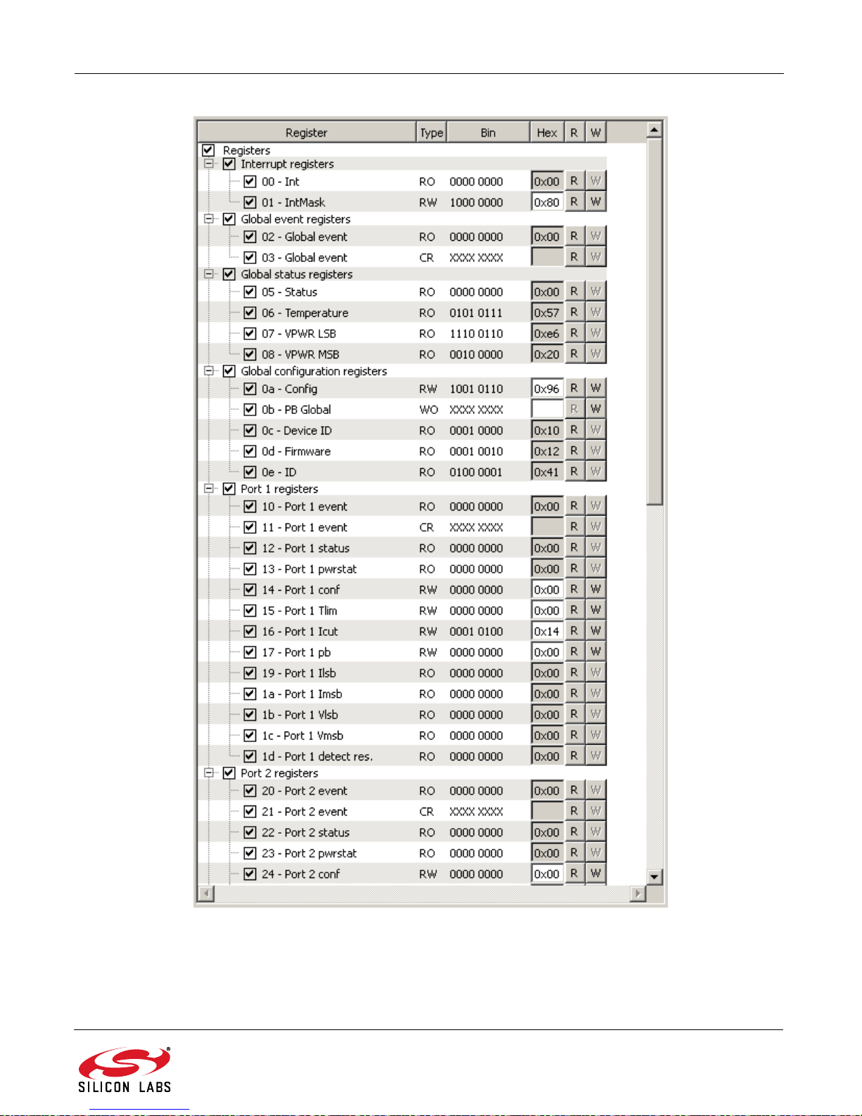
5.7. Register List
The Register List shown in Figure 14 displays the contents of the Si3454 registers and allows the user to change
the register contents.
12 Confidential Rev. 0.1
Page 13
Si3454-KIT
The Register List displays all of the Si3454’s registers grouped by category. Each category of registers can be
expanded and collapsed by clicking on the plus and minus signs at the left edge of the Register List.
Next to the register name, the type of each register is displayed. Each register is either RW (read/write), RO (read
only), WO (write only) or CR (Clear on Read). WO registers reflect the value applied by the user.
Figure 14. Register List
Confidential Rev. 0.1 13
Page 14

Si3454-KIT
The user may specify which registers to read (when the GUI is updated) by checking a box at the left of each
register name. Refreshing, polling, and RoM, all depend on these settings. Clear on Read registers are read only if
both the CoR check box is checked and the check box for the individual CR register is checked.
The user may read and write individual registers by using the “ R” ( re ad) a nd “W” ( write ) button s at the rig ht ed ge of
each register. The “R” and “W” buttons are disabled if the operation is not allowed for the type of register. The
display of the whole register file can be read and updated at once by clicking on the “Refresh” button.
The Register List displays the value of each register in binary and hexadecimal form. If a register has not yet been
read, then its binary value is displayed as all Xs, and its hexadecimal value is blank.
A register's hexadecimal value is displayed in a text box. If a register is not writable (RO or CR), then its text box is
gray and its hexadecimal value cannot be changed by the user. If a register is writable (RW), then its text box is
white and its hexadecimal value can be changed by the user. After changing a register's value, the user clicks on
the register's “W” button to write the new value to the register.
14 Confidential Rev. 0.1
Page 15

Si3454-KIT
6. Operating the System
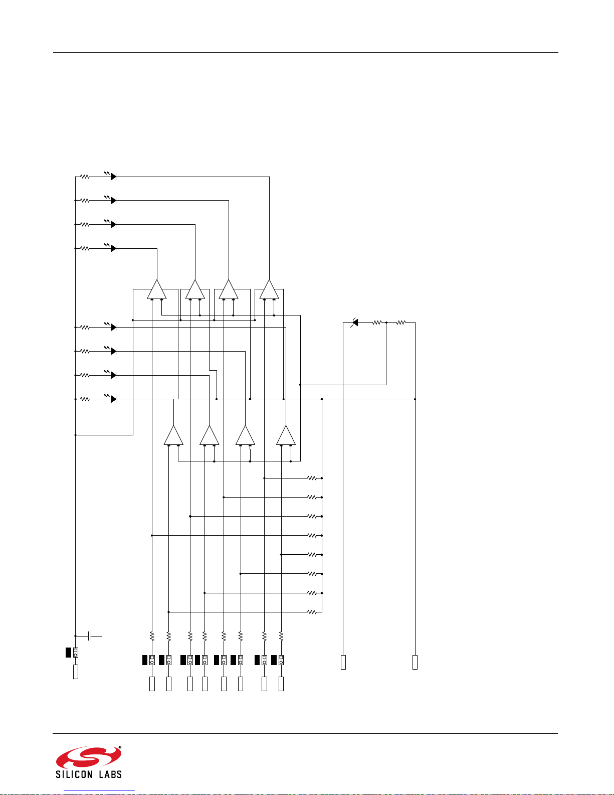
Each RJ45 connector board has eight LEDs for the eight ports. Each LED is driven by a comparator circuit which
detects when a voltage is forced to the load at the PoE output. When the ports are in auto mode, the LEDs in the
RJ45 connector board flash, indicating the detection cycle until a valid PD is connected. Once a valid PD is
connected and the port is turned on, the LEDs will glow steadily until the PD is disconnected. Once the PD is
connected, the port current will be displayed on the GUI. Note that the comparator circuits load the ports slightly,
and the LEDs dissipate power from the 3.3 V rail. If performing calibrated tests, it may be desirable to isolate the
comparator circuitry and eliminate any loading. This may be done by removing all jumpers from the co nnector
board.
The easiest way to get started is to put all of the ports in Auto mode. In Auto mode, detection, classification, power
management based on classification (Icut setting), disconnect (when enabled by “Disconnect Enable”), fault
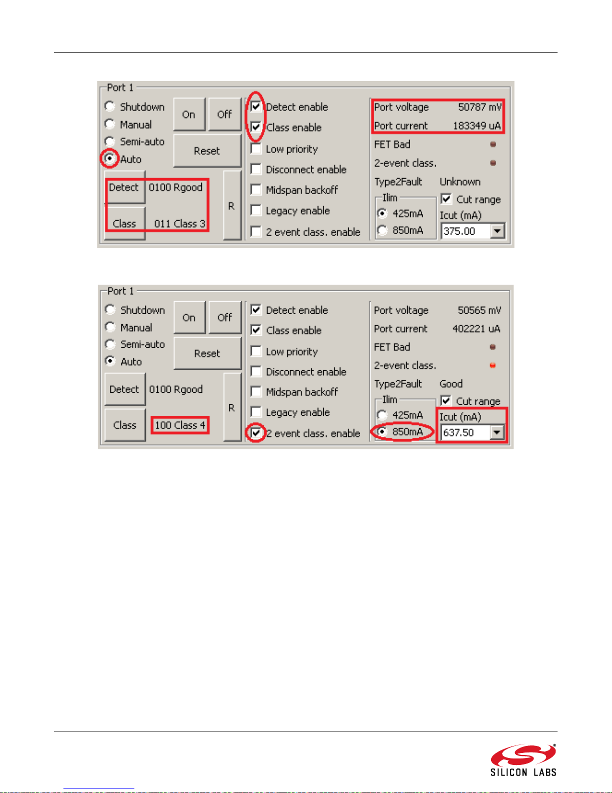
protection, fault recovery, and port monitoring all happen without user intervention. Figure 15 shows the result of
putting Port 1 in Auto mode. Circles indicate the required settings, and the squares indicate that a PD connected to
the port has been detected, classified, and powered. Auto mode may also be enabled on all ports by configuring
J10 and resetting the board by pressing SW1 or cycling power.
The Si3454 normally operates in manual or semi-automatic mode with the AUTO pin is held low. If a positive
voltage is applied to the AUTO pin, the Si3454 enters into fully autonomous operation, independent of a host. The
Si3454 also features dc disconnect detection algorithms to determine when a PD device is disconnected from any
of the eight independent ports. The AUT O mode can be set via the AUT O pin or from the host via I
the Si3454 reads the voltage on the AUTO pin (which can be set by a resistor divider from VDD to GND). If a
positive voltage is applied, the Si3454 enters into AUTO mode (all ports operate fully autonomously). The AUTO
pin voltage level configures the Si3454’s behavior to register default values. For additional detail on Auto Pin
Configurations, refer to Section 3.2 Operating Modes in the Si3454 data sheet.
If the GUI is left in polling mode, the port status, port current, port voltage are all automatically updated by polling
the appropriate registers of the Si345 4.
The Si3454 itself normally powers up as Alternative A, with no detection back-off, meaning the detect function
cycles at its highest rate. This is the most common usage for the Si3454. The RJ-45 connector board for the
evaluation kit is configured to inject the power on the “spare pairs” of the Ethernet cable, which is the Alternative B
or “Midspan” connection. Detection back-off is intended to ensure that a midspan and an endpoint do not compete
with each other and result in a failure to provide power. With detection back- off, the time be tween detection pulses
is increased to just over two seconds so as not to compete with th e norm al ( appro xim ately th ree times p er se co nd)
detection of an endpoint. If detection back-off is required, click the “Midspan” button to toggle this mode. You will
see that the LEDs on the connector board now flash at the slower detection speed. To toggle the mode back to
standard detection timing, click the button again.
The Si3454 in auto mode is fully-compliant with the 802.3at standard (often called PoE+), which allows up to 30 W
to be delivered over the Ethernet cable. In host-controlled mode, to enable the higher power support for a given
port, it is necessary to make multiple selections as described in "5.5.2. Port Configuration" on page 10. When Auto
mode is selected by the Auto jumper, the Si34 54 a utomatically perfor ms the two-even t classifica tio n and incre ases
the cut-off current if a Class 4 PD is detected. The Si3402 evaluation board provided with the kit is configured to
provide the Class 4 signature; so, if the PoE+ mode is enabled and the Si3402 is plugged in, the cut-off current is
automatically set to 643.2 mA. Figure 16 shows the result of plugging in a Class 4 PD (into Port1) with PoE+ power
enabled. Class 4-specific settings and results are highlighted.
2
C. At power-up,
Confidential Rev. 0.1 15
Page 16
Si3454-KIT
Figure 15. Example Result of Device Connection in Port Auto Mode
Figure 16. Class 4 Connection
16 Confidential Rev. 0.1
Page 17

Si3454-KIT
7. Board Schematics, BOM, and Layout
The following are general PCB layout considerations. Detailed schematics, BOM, and layout can also be found in
the following sections. Visit the Silicon Labs Technical Support web page and register to submit a technical support
request, particularly if you are not closely following the recommended reference design.
7.1. Design and Layout Considerations
The Si3454 directly drives and senses detection and classification stimulus voltages. PoE power is enabled
through external FETs. PoE power supply currents in each channel are sensed using current shunt resistors with
sensed voltage referenced to GND.
Normally the layout will be 4-layer, with dedicated VPWR and GND planes for PoE power delivery. The ground
power plane does not generally have a high frequency content; so, it is acceptable to use a single GND plane and
tie GND, AGND, DGND pins to it. The thermal pad of the Si3454 is connected to GND. Si3454 internal dissipation
is modest, but for best performance the layout should include a thermal bond consisting of multiple vias between
the thermal pad and GND. The PoE power MOSFETs carry up to 800 mA dc and up to 5 A in faults; so, a 20 mil
trace with wide or multiple vias is also recommended.
The Si3454 includes a buck type dc-dc converter controller function, which generates a raw ~4 V power rail VCAP.
The buck regulator is able to supply 200 mA; so, within a group of Si3454 devices, only one buck regulator is
required. The single buck regulator supplies low drop-out (LDO) regulators within individual Si3454 devices to
generate their VDD = 3.3 V. Each LDO supplies the 3.3 V requirements of its own Si3454. The Si3454 VDD LDO is
able to supply additional current for an external device, such as an isolator or low-power-management
microcontroller.
The Si3454 buck regulator is a potent ial EMI source. The power devices, e.g. switching MOSFET, inductor, diode
and output capacitor should be located as close together as possible to minimize loop area. The entire switching
circuit should be shielded from Si3454 port connections to minimize the chance of interference.
To improve sensing accuracy, the Si3454 provides Kelvin connections for the r esistor low side sense. The SENSEx
signals are connected to GND potential, but for best performance they should be routed separately from the GND
plane.
To avoid coupling between surge events and logic signals, it is recommended that VOUTn traces be well separated
2
C interface pins.
from I
A typical layer stackup is as follows:
1. Top: I
2. VPWR, VDD = 3.3 V
3. VEE = GND
4. Bottom: VOUT, switcher, VCAP
2
The I
C bus runs at 400 kHz maximum. The I2C bus lines should be routed away from analog lines like Rbias or
Vref but can otherwise be routed with ordinary care. If using a Silicon Labs I
the connections as per the reference design, which take into account r equired voltage margins and pullup values.
2
C, Si3454 Kelvin current sense
2
C isolation product, please observe
Confidential Rev. 0.1 17
Page 18
Si3454-KIT
3.3V Status
INPUT
POWER
BULK DECOUPLING
Isolation bypass
UNISOLATED
3.3V_1 Status
To PoE magnetics and LEDs
Inter-Board
Chain
Isolate Buck
Components
When Chained
Disable Buck
when Chained
Remove
Pullups
When
Chained
Disable
Buck
Disable Drive
When Chained
Enable Buck for
Single Board
Layout Notes:
1. Make loop containing C113, R134, M1,
L1, R16, C12 as small as possible.
2. Make loop containing D4, L1, R16, C12
as small as possible.
SCL
SDA
SCL
/INT
CAP
VOUT1
VOUT2
VOUT3
VOUT4
VOUT9
VOUT10
VOUT11
VOUT12
SDA
/INT
CAP
SDA
SCL
/INT
/SHDN
/RESET
/SHDN
/RESET
AUTO
AUTO
+3V3
+3V3
VPWR
VPWR
+3V3
+3V3LV
+3V3+3V3LV
+3V3LV
+3V3LV +3V3
+3V3
+3V3_1
VPWR
+3V3_1
VPWR
+3V3_1
+3V3
VPWR
VPWR
VPWR
+3V3
VPWR
+3V3
400 W Cesar Chavez
Austin, TX 78701
400 W Cesar Chavez
Austin, TX 78701
400 W Cesar Chavez
Austin, TX 78701
J8
HEADER 8x2
1 2
3 4
5 6
7 8
9 101113
15
121416
C110
10uF
D3
GREEN
3.3V PWR
C101
680pF
R3
1K
C112
0.1uF
JS18
JS10
JS7
C3
0.1uF
NI
+3V3
JS19
TP7
GND
BLACK
TPV1
D2
MBRS3100T3
JS11
JS20
J3
CONN TRBLK 2
1
2
R106
330
R1
10K
NI
R108 0NI
TP1
SDA
BLACK
SW1
SW PUSHBUTTON
C102
680pF
J5
HEADER 4x3
1
234
567
8910
11
12
JS12
TPV3
R17
330
JP10
Port_Drive_1
Si3454
SCL
SDA
VPWR
GND
VDD
VOUT1
VOUT2
VOUT3
VOUT4
/INT
A1
A2A3A0
SWO
CAP
/RESET
AUTO
/SHDN
/DCEN
ISENSE
JP3
JS13
M1
FQT5P10
R132 0
TP3
INT
BLACK
D1 ES1BNI
C7
10uF
C111
0.1uF
D5
GREEN
3.3V PWR_1
TPV4
+
C11
33uF
JP7
JS1
JS14
TP8
GND
BLACK
JP11
TP4 RST
BLACK
JS2
JS15
JP12
J1
HEADER 4x3
1
234
567
8910
11
12
R18
44.2K
R133
10K
TP21
CAP
BLACK
D4
ES1B
JS3
JS9
C4
0.1uF
JS16
+
C9
33uF
+
C10
33uF
JP13
R1393.24K
L1
100uH
JS4
J2
HEADER 5x2
1
1
2
2
3
3
4
4
5
5
6
6
7
7
8
8
9
9
10
10
R1406.49K
JS5
JP9
R2
10K
C1
1uF
JS8
J9
HEADER 10x2
1 2
3 4
5 6
7 8
9 10
11 12
13 14
15 16
17 18
19 20
ISOLATION
U1
Si8605
VDD1
1
VDD2
16
GND2
9
GND1
8
NC
2
NC
15
A13A2
4
B312B4
11
A35A4
6
B114B2
13
NC
7
NC
10
R14113.0K
JP6
C8
0.1uF
JS6
JP8
C12
10uF
R14226.1K
+3V3_1
R134
1.0
R16
0
JP14
TPV2
TP2
SCL
BLACK
R4
1K
+
C113
33uF
C2
1uF
R5
1K
TP6
GND
BLACK
J10
HEADER 4x3
1
2
3
4
5
6
7
8
9
10
11
12
Port_Drive_0
Si3454
SCL
SDA
VPWR
GND
VDD
VOUT1
VOUT2
VOUT3
VOUT4
/INT
A1
A2A3A0
SWO
CAP
/RESET
AUTO
/SHDN
/DCEN
ISENSE
JS17
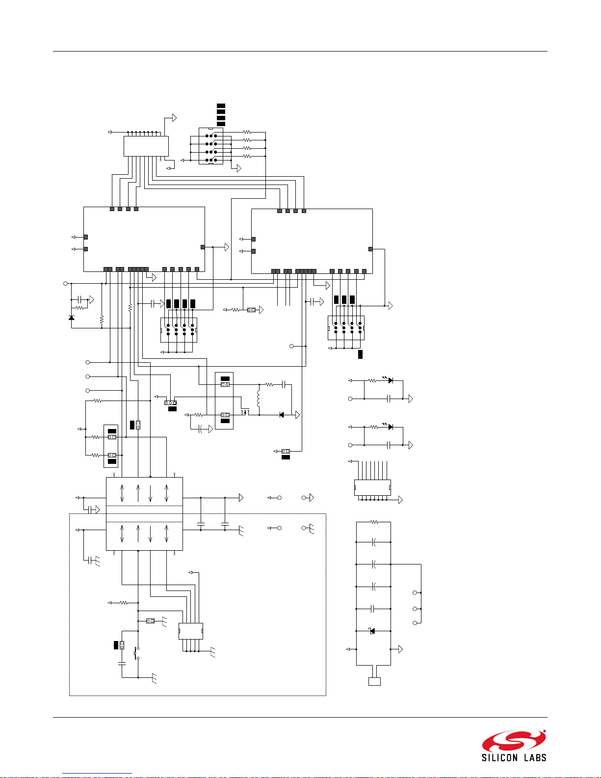
7.2. Si3454 Schematics
18 Confidential Rev. 0.1
Figure 17. Evaluation Board Top Level
Page 19
Si3454-KIT
VPWR
GND
GND
VPWR
GND
GND
SCL
SDA
GND
/RESET
VPWR
VDD
/INT
/SHDN
AUTO
VOUT1
VOUT2
VOUT3
VOUT4
SWO
CAP
/DCEN
ISENSE
A1A2A3
A0
C16
0.1uF
TP16
VOUT2
C20
0.1uF
TP11
GATE2
R81 0.25
D23
SMAJ58A
C21
0.1uF
R84 0.25
TP17
VOUT3
D21
SMAJ58A
C22
0.1uF
R87 0.25
TP9
GATE1
TP18
VOUT4
Q2 FDMC3612
TP12
GATE3
D24
SMAJ58A
TP13
VOUT1
R92 0.25
Si3454
U2
KSENSA
8
RESET31A336A134A235A0
33
VDDA
14
EPAD
39
VDD
30
INT
32
DRAIN17DRAIN29DRAIN3
24
GATE4
28
GATE1
5
SENSE2
10
GATE3
22
SENSE4
27
SENSE1
6
GATE2
11
SENSE3
23
DRAIN4
26
KSENSB
25
SWO17CAP
18
SDAI38SDAO1SCL37SHDN
2
AUTO
3
VPWR
13
AGND
16
AGND
12
NC15NC
4
DCEN
19
ISENSE
20
DGND
29
AGND
21
Q3 FDMC3612
D22
SMAJ58A
TP10
GATE4
C17
10uF
C18
0.1uF
C15
0.1uF
Q1 FDMC3612
Q4 FDMC3612
C19
10uF
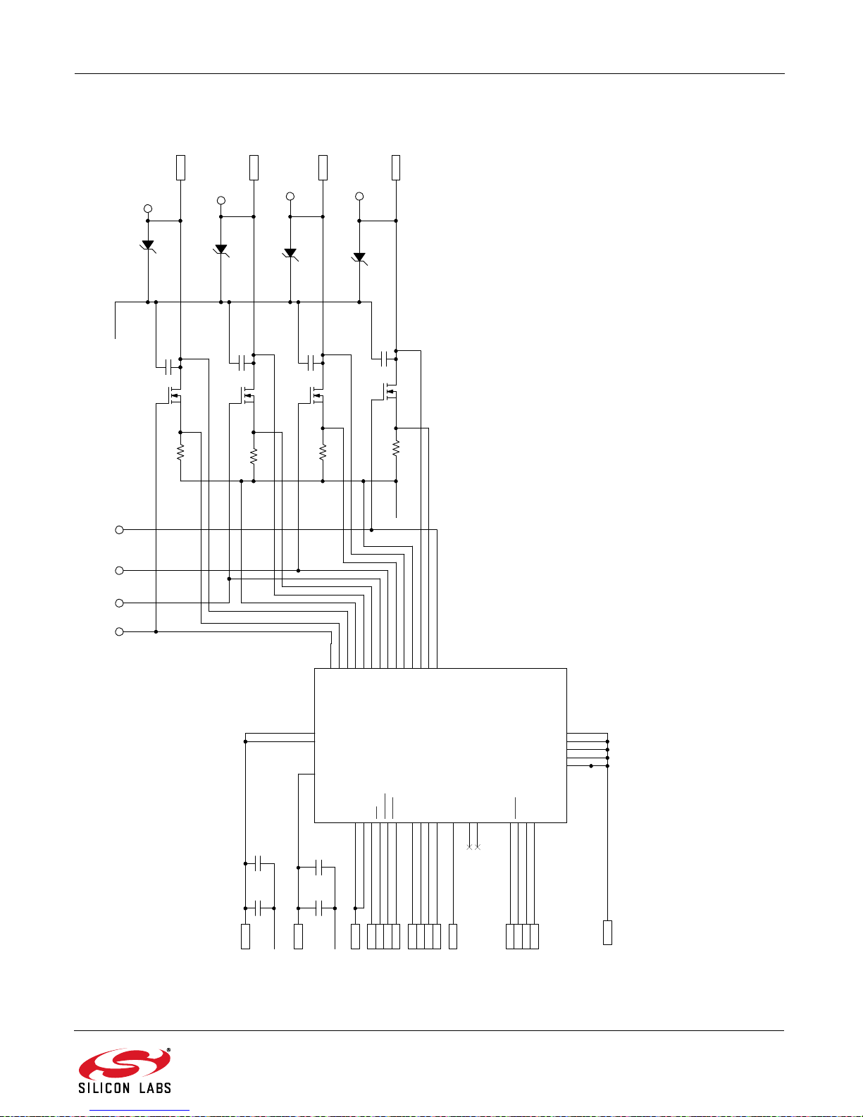
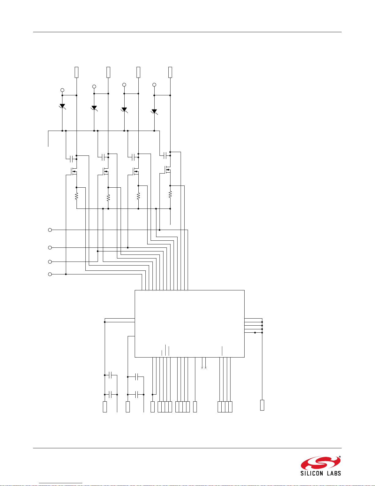
Figure 18. Si3454 Controllers (1 of 2)
Confidential Rev. 0.1 19
Page 20
Si3454-KIT
VPWR
GND
GND
VPWR
GND
GND
SCL
SDA
GND
/RESET
VPWR
VDD
/INT
/SHDN
AUTO
VOUT1
VOUT2
VOUT3
VOUT4
SWO
CAP
/DCEN
ISENSE
A1A2A3
A0
C29
0.1uF
TP36
VOUT2
C33
0.1uF
TP31
GATE2
R107 0.25
D31
SMAJ58A
C34
0.1uF
R110 0.25
TP37
VOUT3
D29
SMAJ58A
C35
0.1uF
R113 0.25
TP29
GATE1
TP38
VOUT4
Q10FDMC3612
TP32
GATE3
D32
SMAJ58A
TP33
VOUT1
R118 0.25
Si3454
U3
KSENSA
8
RESET31A336A134A235A0
33
VDDA
14
EPAD
39
VDD
30
INT
32
DRAIN17DRAIN29DRAIN3
24
GATE4
28
GATE1
5
SENSE2
10
GATE3
22
SENSE4
27
SENSE1
6
GATE2
11
SENSE3
23
DRAIN4
26
KSENSB
25
SWO17CAP
18
SDAI38SDAO1SCL37SHDN
2
AUTO
3
VPWR
13
AGND
16
AGND
12
NC15NC
4
DCEN19ISENSE
20
DGND
29
AGND
21
Q11FDMC3612
D30
SMAJ58A
TP30
GATE4
C30
10uF
C31
0.1uF
C28
0.1uF
Q9 FDMC3612
Q12FDMC3612
C32
10uF
20 Confidential Rev. 0.1
Figure 19. Si3454 Controllers (2 of 2)
Page 21
7.3. Si3454 Evaluation Board Layout
Si3454-KIT
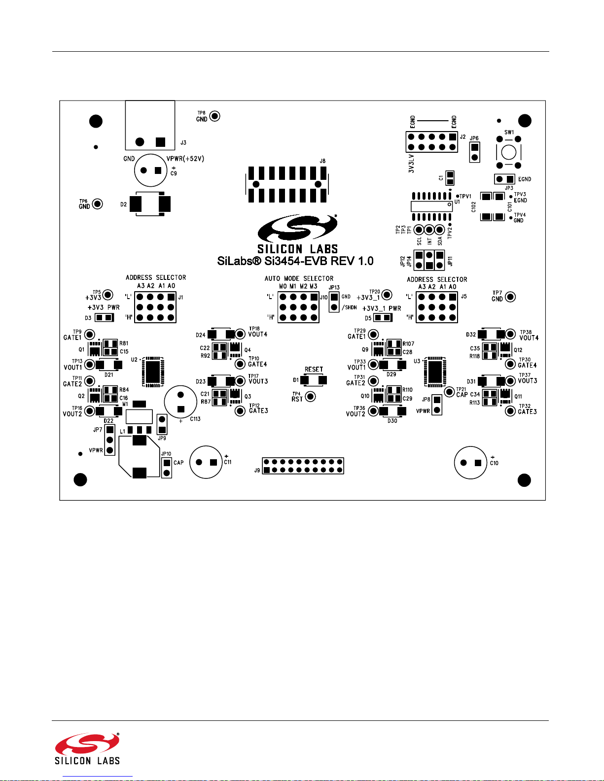
Figure 20. Evaluation Board Top Silkscreen
Confidential Rev. 0.1 21
Page 22
Si3454-KIT
22 Confidential Rev. 0.1
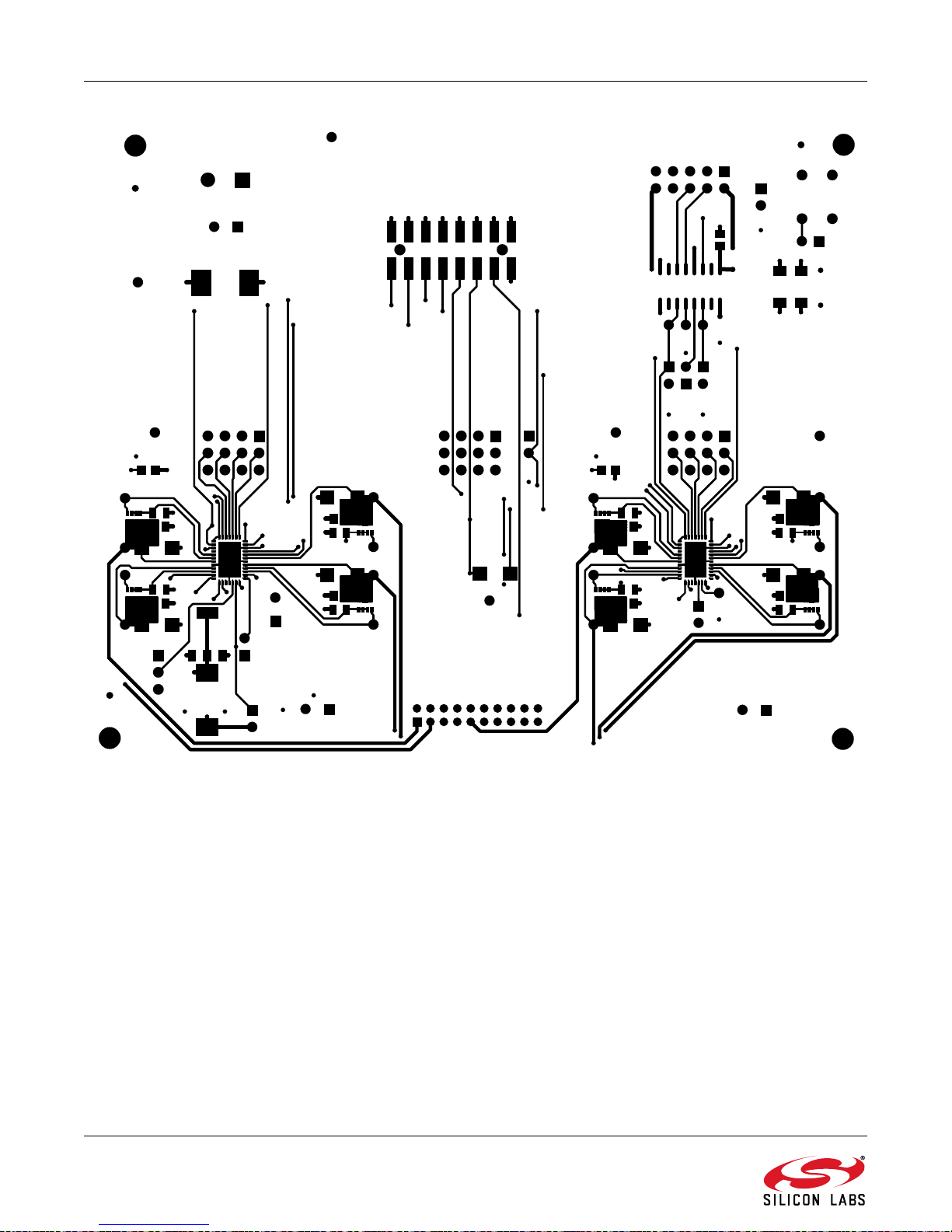
Figure 21. Evaluation Board Top Side
Page 23
Si3454-KIT
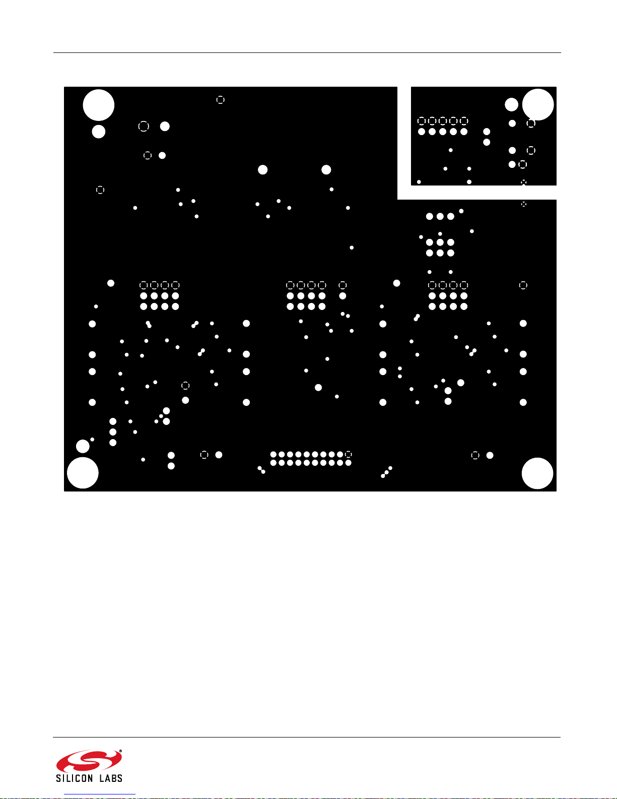
Figure 22. Evaluation Board Ground Layer
Confidential Rev. 0.1 23
Page 24
Si3454-KIT
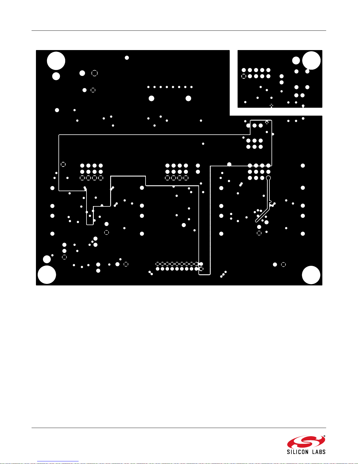
Figure 23. Evaluation Board Power Layer
24 Confidential Rev. 0.1
Page 25
Si3454-KIT
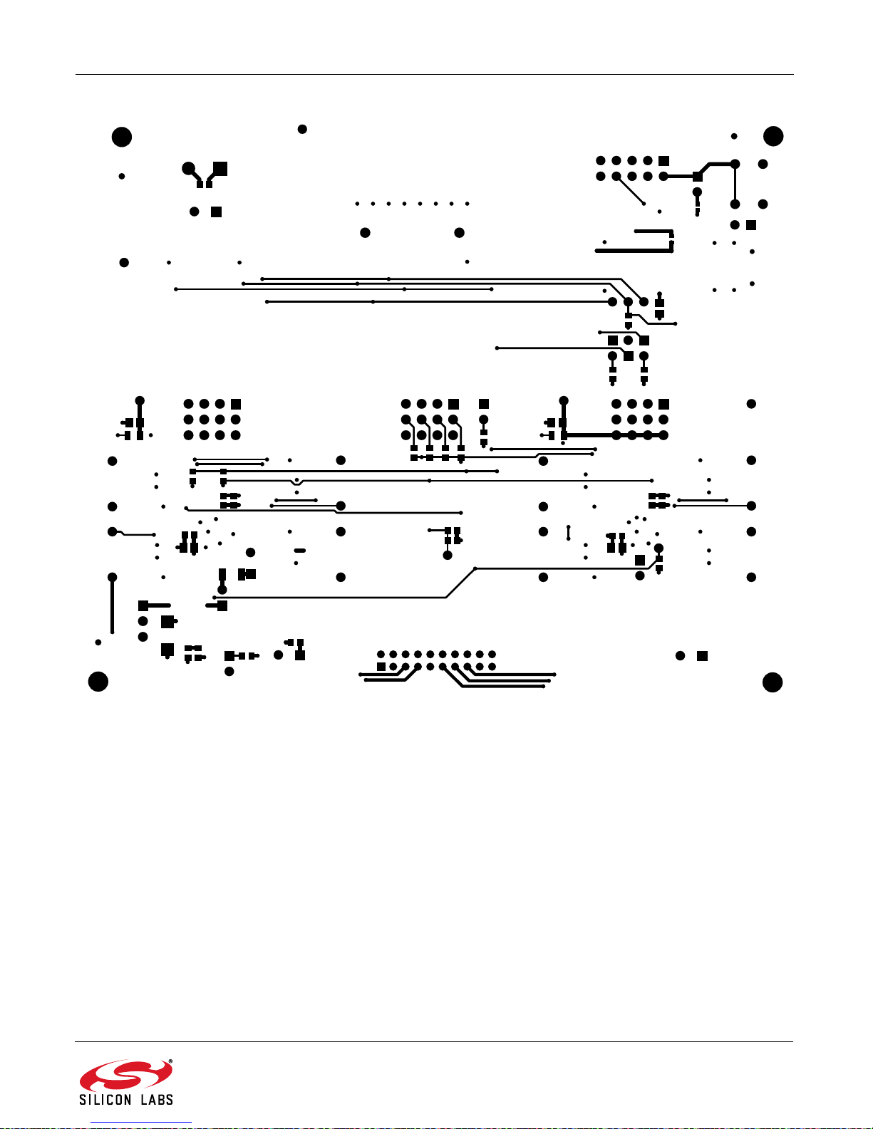
Figure 24. Evaluation Board Bottom Side
Confidential Rev. 0.1 25
Page 26

Si3454-KIT
7.4. Si3454 Bill of Materials
Table 3. Si3454 Evaluation Board Bill of Materials
Qty Ref Value Rating Voltage/C
urrent
2 C1,C2 1uF 16V ±20% X7R C0805 C0805X7
4C3,C8,
C111,
C112
1 C4 0.1uF 10V ±10% X7R C0402 C0402X7
2 C7,C1 10 10uF 10V ±20% X5R C0805 C0805X5
4C9,C10,
C1 1,C113
5 C12,C17,C19,C
30,C32
10 C15,C16,C20,C
21,C22,C28,C2
9,C33,C34,C35
0.1uF 100V ±20% X7R C0603 C0603X7
33uF 100V ±20% Alum_ElecC3.5X8M
10uF 10V ±10% X5R C0603 C0603X5
0.1uF 100V ±10% X7R C0805 C0805X7
Tol Type PCB
Footprint
M-RAD
Mfr Part
Number
R160-105
M
R101-104
M
R100-104
K
R100-106
M
ECA2AM
330
R100-106
K
R101-104
K
Mfr
Venkel
Venkel
Venkel
Venkel
Panasonic
Venkel
Venkel
2 C18,C31 0.1uF 16V ±20% X7R C0603 C0603X7
R160-104
M
2 C101,
C102
2 D1,D4 ES1B 1.0A 100V Fast DO-214ACES1B Diodes Inc.
1 D2 MBRS310
2 D3,D5 GREEN 30mA 2.2V SMT LED-0805-KLTST-C17
8 D21,D22,D23,D
24,D29,D30,D3
1,D32
9JP3,JP6,
JP8,JP9,
JP10,
JP11,JP12,
JP13,JP14
680pF Y3 250V ±15% Y3 C1808 GA342Q
R7GD681
KW01L
3A 100V Schottky DO-214ABMBRS310
0T3
SMAJ58A 400W 58V GP DO-214ACSMAJ58A Littelfuse
JUMPER Header CONN1X2TSW-102-
0T3
0GKT
07-T-S
Venkel
MuRata
On Semi
LITE_ON INC
Samtec
26 Confidential Rev. 0.1
Page 27

Si3454-KIT
Table 3. Si3454 Evaluation Board Bill of Materials (Continued)
Qty Ref Value Rating Voltage/C
urrent
1 JP7 HEADER
1x3
20 JS1,JS2,JS3,J
S4,JS5,JS6,JS
7,JS8,JS9,JS10
,JS11,JS12,JS1
3,JS14,JS15,JS
16,JS17,JS18,J
S19,JS20
3 J1,J5,J10 HEADER
1 J2 HEADER
1J3CONN
1 J8 HEADER
1 J9 HEADER
Jumper
Shunt
4x3
5x2
TRBLK 2
8x2
10x2
Tol Type PCB
Footprint
Header CONN-1X3TSW-103-
Shunt N/A SNT-100-
Header CONN3X4TSW-104-
Header CONN2X5TSW-105-
TERM
BLK
MALE
Header CONN2X
Header CONN2X
CONN-TB
-1757242
8-TSM
10-2MM
Mfr Part
Number
07-T-S
BK-T
07-G-T
07-T-D
1757242 PHOENIX CON-
TSM-108-
01-T-DV
TMM-110-
01-T-D
Mfr
Samtec
Samtec
Samtec
Samtec
TACT
Samtec
Samtec
1 L1 100uH 1.0 A ±2 0% Shielded IND-CTSL
F1045
4MH1,MH2,
MH3,MH4
1 M1 FQT5P10 1.0A 100V P-CHNL SOT223-
1 PCB1 Si3454-E
8 Q1,Q2,Q3,
Q4,Q9,Q10,Q1
1,Q12
3 R1,R2,R133 10K 1/10W ±1% ThickFilm R0603 CR0603-1
2 R3,R4 1K 1/10W ±1% ThickFilm R0603 CR0603-1
1 R5 1K 1/16W ±5% ThickFilm R0402 CR0402-1
4-40 HDW MH-125NPNSS-4-4-01Richco Plastic
GDS
BARE
VB REV
1.0
FDMC361212A 100V N-CHNL POW-
PCB
N/A Si3454-E
ER33
CTSLF10
45-101M
FQT5P10 Fairchild
VB REV
1.0
FDMC361
2
0W-1002
F
0W-1001
F
6W-102J
Central Tech
Co
SiLabs
Fairchild
Venkel
Venkel
Venkel
Confidential Rev. 0.1 27
Page 28

Si3454-KIT
Table 3. Si3454 Evaluation Board Bill of Materials (Continued)
Qty Ref Value Rating Voltage/C
urrent
3 R16,R108,
R132
2 R17,R106 330 1/10W ±1% ThickFilm R0805 CR0805-1
1 R18 44.2K 1/10W ±1% ThickFilm R0603 CR0603-1
8 R81,R84,R87,R
92,R107,
R110,R113,
R118
1 R134 1 1/4W ±1% ThickFilm R1206 CR1206-4
1 R139 3.24K 1/10W ±1% ThickFilm R0603 CR0603-1
1 R140 6.49K 1/16W ±1% ThickFilm R0603 CR0603-1
0 1A ThickFilm R0603 CR0603-1
0.25 1/4W ±1% ThickFilm R0805 LCR0805-
Tol Type PCB
Footprint
Mfr Part
Number
6W-000
0W-3300
F
0W-4422
F
R250F
W-1R00F
0W-3241
F
6W-6491
F
Mfr
Venkel
Venkel
Venkel
Venkel
Venkel
Venkel
Venkel
1 R141 13.0K 1/16W ±1% ThickFilm R0603 CR0603-1
6W-1302
F
1 R142 26.1K 1/16W ±1% ThickFilm R0603 CR0603-1
6W-2612
F
4 SO1,SO2,
SO3,SO4
1SW1SW
4 TPV1,TPV2,
TPV3,TPV4
STAND-
OFF
50mA 12Vdc Tactile SW4N6.5
PUSH-
BUTTON
TPV PCB Fea-
HDW 2397 SPC Technology
101-0161-EVMountain Switch
X4.5-PB
VIA-TP N/A N/A
ture
Venkel
Venkel
28 Confidential Rev. 0.1
Page 29

Si3454-KIT
Table 3. Si3454 Evaluation Board Bill of Materials (Continued)
Qty Ref Value Rating Voltage/C
urrent
24 TP1,TP2,TP3,T
P4,TP6,TP7,
TP8,TP9,TP10,
TP1 1,TP12,
TP13,TP16,
TP17,TP18,
TP21,TP29,
TP30,TP31,
TP32,TP33,
TP36,TP37,
TP38
2 TP5,TP20 RED Loop TEST-
1 U1 Si8605 3750
2 U2,U3 Si3454 50V PSE QFN38N5
BLACK Loop TEST-
VRMS
Tol Type PCB
Footprint
POINT
POINT
Isolator SO16N6.
0P1.27
X7P0.5
Mfr Part
Number
151-203-
RC
151-207-
RC
Si8605AC
-B-IS1
Si3454-A-
FM
Mfr
Kobiconn
Kobiconn
SiLabs
SiLabs
Confidential Rev. 0.1 29
Page 30
Si3454-KIT
VOUT1
VOUT2
VOUT3
VOUT4
VOUT5
VOUT6
VOUT7
VOUT8RTN8
RTN1
RTN2
RTN3
RTN4
RTN5
RTN6
RTN7
RTN8
RTN1
RTN2
RTN3
RTN4
RTN5
RTN7
RTN6
+3V3
VPWR
PoE LEDs
PoE LEDs
+3V3
GND
VOUT1
VOUT2
VOUT3
VOUT4
VOUT5
VOUT6
VOUT7
VOUT8
VPWR
POE_OUT
POE_OUT
VOUT1
VOUT2
VOUT3
VOUT4
VOUT5
VOUT6
VOUT7
VOUT8
RTN1
RTN2
RTN3
RTN4
RTN5
RTN6
RTN7
RTN8
J1
HEADER 10x2
12
34
56
78
910
1112
1314
1516
1718
1920
7.5. RJ45 Connector Board Schematics
30 Confidential Rev. 0.1
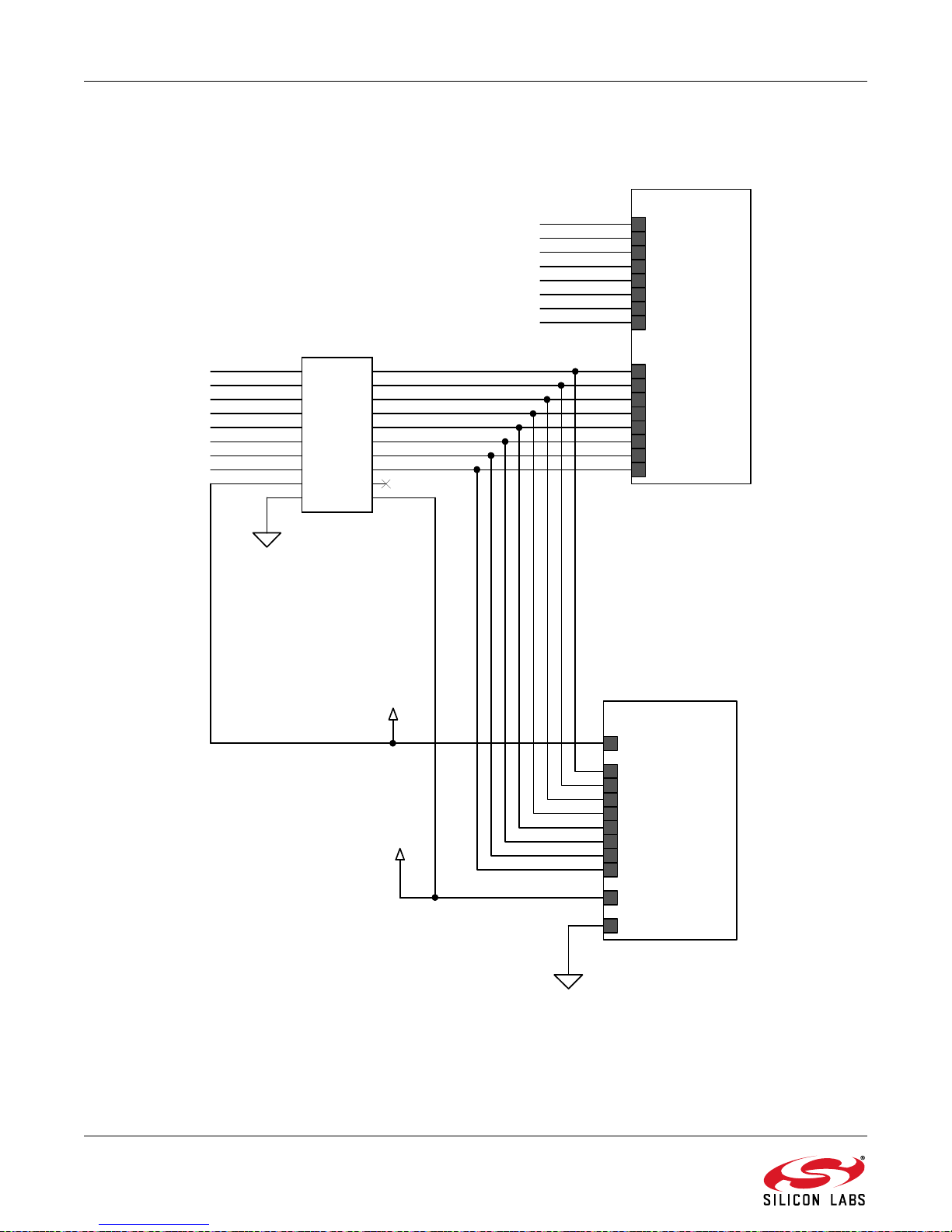
Figure 25. Connector Board Top Level
Page 31
Si3454-KIT
This circuit faci litates visualization of PoE test voltages applied by
the PoE controller. It introduces some minor error in port detecti on
voltage, which may be eliminated by jumper disconnection. This
circuit is not intended to be included in production designs.
Remove jumpers JP1...JP8 to prevent any loading
on the port. Remove JP9 to prevent LEDs from
turning on when JP1...JP8 are removed.
CMP_REF
GND
GND
+3V3
GND
VOUT1
VOUT2
VOUT3
VOUT4
VOUT5
VOUT6
VOUT7
VOUT8
VPWR
JS7
D201
GREEN
D200
GREEN
R211
4.99M
R222
332
D207
GREEN
+
-
V+
V-
U201A
LMX393H
1
2
3
4 8
R201
200K
R221
332
JS8
JP5
R214
4.99M
D205
GREEN
R203
200K
D208
5.1V
+
-
U201B
LMX393H
5
6
7
R224
40.2K
JP9
R200
200K
JP6
JS9
R218
332
R205
200K
JS2
JP2
+
-
V+
V-
U203A
LMX393H
1
2
3
4 8
R212
4.99M
JP7
C200
1uF
R209
4.99M
R207
200K
JS3
R215
4.99M
+
-
V+
V-
U202A
LMX393H
1
2
3
4 8
JP8
R217
332
R223
332
R225
1M
JS4
D203
GREEN
JP3
+
-
U203B
LMX393H
5
6
7
R202
200K
R220
332
+
-
V+
V-
U204A
LMX393H
1
2
3
4 8
R213
4.99M
+
-
U204B
LMX393H
5
6
7
JP4
JS5
R210
4.99M
R204
200K
R219
332
D206
GREEN
JS1
+
-
U202B
LMX393H
5
6
7
R208
4.99M
D204
GREEN
R206
200K
JS6
R216
332
D202
GREEN
JP1
Figure 26. Connector Board Comparators and LEDs
Confidential Rev. 0.1 31
Page 32
Si3454-KIT
VOUT1
VOUT2
VOUT3
VOUT4
VOUT5
VOUT6
VOUT7
VOUT8
RTN1
RTN2
RTN3
RTN4
RTN5
RTN6
RTN7
RTN8
L306A
FA2536-ALD
1
2
3
L301A
FA2536-ALD
1
2
3
J301D
RJ-45
MX0+
D1
MX0-
D2
MX1+
D3
MX2+
D4
MX2-
D5
MX1-
D6
MX3+
D7
MX3-
D8
C3230.1uF
L300A
FA2536-ALD
1
2
3
C3190.1uF
J300D
RJ-45
MX0+
D1
MX0-
D2
MX1+
D3
MX2+
D4
MX2-
D5
MX1-
D6
MX3+
D7
MX3-
D8
C3140.1uFC3100.1uF
C3280.1uF
J301H
RJ-45
MX0+
H1
MX0-
H2
MX1+
H3
MX2+
H4
MX2-
H5
MX1-
H6
MX3+
H7
MX3-
H8
C3240.1uF
J301A
RJ-45
MX0+
A1
MX0-
A2
MX1+
A3
MX2+
A4
MX2-
A5
MX1-
A6
MX3+
A7
MX3-
A8
J300H
RJ-45
MX0+
H1
MX0-
H2
MX1+
H3
MX2+
H4
MX2-
H5
MX1-
H6
MX3+
H7
MX3-
H8
J300A
RJ-45
MX0+
A1
MX0-
A2
MX1+
A3
MX2+
A4
MX2-
A5
MX1-
A6
MX3+
A7
MX3-
A8
L307B
FA2536-ALD
6
5
4
L301B
FA2536-ALD
6
5
4
L305A
FA2536-ALD
1
2
3
L306B
FA2536-ALD
6
5
4
C3150.1uF
L300B
FA2536-ALD
6
5
4
L304A
FA2536-ALD
1
2
3
C3110.1uF
C3290.1uF
C3060.1uF
J301E
RJ-45
MX0+
E1
MX0-
E2
MX1+
E3
MX2+
E4
MX2-
E5
MX1-
E6
MX3+
E7
MX3-
E8
C3250.1uF
C3020.1uF
J300E
RJ-45
MX0+
E1
MX0-
E2
MX1+
E3
MX2+
E4
MX2-
E5
MX1-
E6
MX3+
E7
MX3-
E8
C3200.1uFC3160.1uF
L305B
FA2536-ALD
6
5
4
J301B
RJ-45
MX0+
B1
MX0-
B2
MX1+
B3
MX2+
B4
MX2-
B5
MX1-
B6
MX3+
B7
MX3-
B8
L303A
FA2536-ALD
1
2
3
L304B
FA2536-ALD
6
5
4
J300B
RJ-45
MX0+
B1
MX0-
B2
MX1+
B3
MX2+
B4
MX2-
B5
MX1-
B6
MX3+
B7
MX3-
B8
L302A
FA2536-ALD
1
2
3
C3210.1uF
C3300.1uFC3260.1uF
C3170.1uF
C3070.1uF
J301F
RJ-45
MX0+
F1
MX0-
F2
MX1+
F3
MX2+
F4
MX2-
F5
MX1-
F6
MX3+
F7
MX3-
F8
C3030.1uF
J300F
RJ-45
MX0+
F1
MX0-
F2
MX1+
F3
MX2+
F4
MX2-
F5
MX1-
F6
MX3+
F7
MX3-
F8
C3040.1uFC3000.1uF
L303B
FA2536-ALD
6
5
4
C3120.1uF
C3310.1uF
J301C
RJ-45
MX0+
C1
MX0-
C2
MX1+
C3
MX2+
C4
MX2-
C5
MX1-
C6
MX3+
C7
MX3-
C8
L302B
FA2536-ALD
6
5
4
J300C
RJ-45
MX0+
C1
MX0-
C2
MX1+
C3
MX2+
C4
MX2-
C5
MX1-
C6
MX3+
C7
MX3-
C8
C3080.1uF
C3270.1uF
C3220.1uFC3180.1uF
C3050.1uF
J301G
RJ-45
MX0+
G1
MX0-
G2
MX1+
G3
MX2+
G4
MX2-
G5
MX1-
G6
MX3+
G7
MX3-
G8
C3130.1uF
C3010.1uF
J300G
RJ-45
MX0+
G1
MX0-
G2
MX1+
G3
MX2+
G4
MX2-
G5
MX1-
G6
MX3+
G7
MX3-
G8
C3090.1uF
L307A
FA2536-ALD
1
2
3
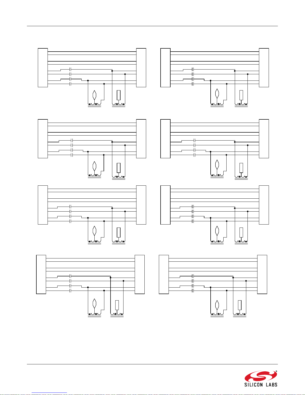
Figure 27. Connector Board Connectors and Coupling Circuits
32 Confidential Rev. 0.1
Page 33
7.6. Connector Board Layout
Si3454-KIT
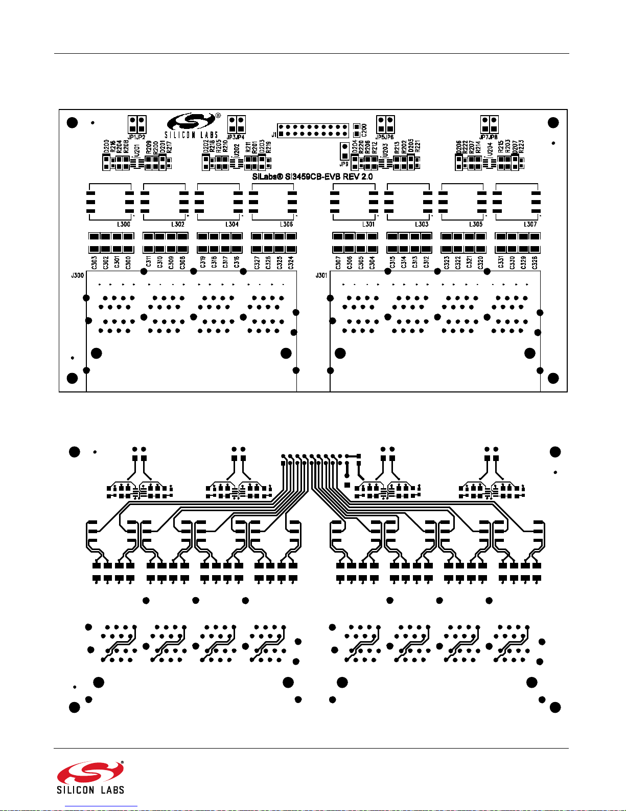
Figure 28. Connector Board Top Silkscreen
Figure 29. Connector Board Top Side
Confidential Rev. 0.1 33
Page 34
Si3454-KIT
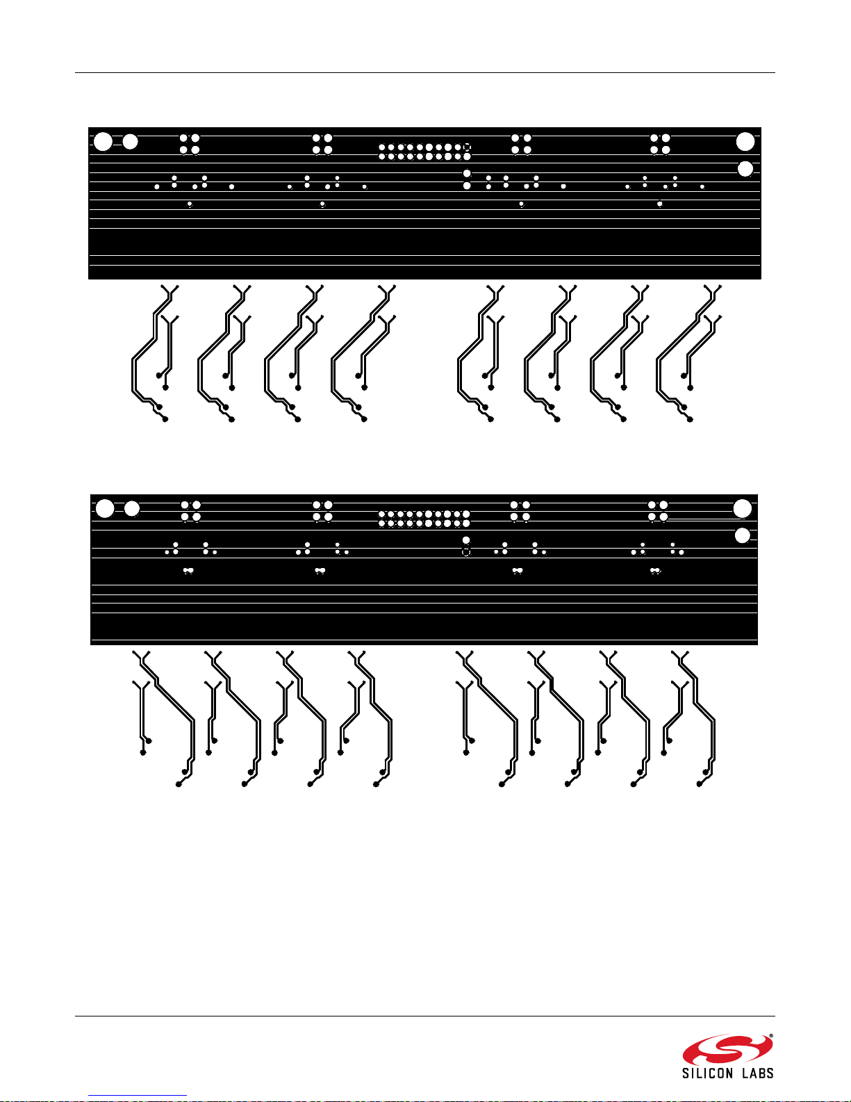
Figure 30. Connector Board Ground Layer
Figure 31. Connector Board Power Layer
34 Confidential Rev. 0.1
Page 35
Si3454-KIT
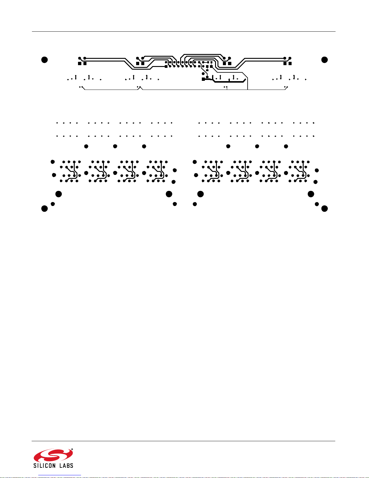
Figure 32. Connector Board Bottom Side
Confidential Rev. 0.1 35
Page 36

Si3454-KIT
7.7. Connector Board Bill of Materials
Table 4. Connector Board Bill of Materials
Qty Ref Value Rating Voltage/
Current
1 C200 1 µF 16 V ±20% X7R C0805 C0805X7R160-105M Venkel
32 C300, C301,
C302, C303,
C304, C305,
C306, C307,
C308, C309,
C310, C311,
C312, C313,
C314, C315,
C316, C317,
C318, C319,
C320, C321,
C322, C323,
C324, C325,
C326, C327,
C328, C329,
C330, C331
8 D200, D201,
D202, D203,
D204, D205,
D206, D207
1 D208 5.1 V 500 mW 5.1 V 5% Zener SOD-123 MMSZ4689T1G On Semi
0.1 µF 250 V ±20% X7R C1210 C1210X7R251-104M Venkel
Green 30 mA 2.2 V SMT LED-0805-K LTST-C170GKT Lite On
Tol Type PCB Footprint Mfr Part Number Mfr
1 J1 Header 10x2 Header CONN2X10-2MM TMM-110-01-T-D Samtec
2 J300 RJ–45 Receptacle RJ45-8PORT 44170-0001 Molex
9 JP1, JP2,
JP3, JP4,
JP5, JP6,
JP7, JP8,
JP9
9 JS1, JS2,
JS3, JS4,
JS5, JS6,
JS7, JS8,
JS9
8 L300, L301,
L302, L303,
L304, L305,
L306, L307
4MH1, MH2,
MH3, MH4
Jumper Header CONN1X2 TSW-102-07-T-S Samtec
Jumper Shunt Shunt N/A SNT-100-BK-T Samtec
FA2536-ALD 675 µH Ethernet IND-FA2536 FA2536-ALD Coilcraft
4–40 HDW NSS-4-4-01 Richco
Plastic Co.
36 Confidential Rev. 0.1
Page 37

Table 4. Connector Board Bill of Materials (Continued)
Si3454-KIT
Qty Ref Value Rating Voltage/
Current
8 R200, R201,
R202, R203,
R204, R205,
R206, R207
8 R208, R209,
R210, R211,
R212, R213,
R214, R215
8 R216, R217,
R218, R219,
R220, R221,
R222, R223
1R224 40.2k 1/10 W ±1% ThickFilm R0603 CR0603-10W-4022F Venkel
1R225 1M 1/10 W ±1% ThickFilm R0805 CR0805-10W-1004F Venkel
4SO1, SO2,
SO3, SO4
4 U201, U202,
U203, U204
200 k 1/10 W ±1% ThickFilm R0805 CR0805-10W-2003F Venkel
4.99 M 1/8 W ±1% ThickFilm R0805 CR0805-8W-4994FT Venkel
332 1/10 W ±1% ThickFilm R0603 CR0603-10W-3320F Venkel
Standoff HDW 2397 SPC_Technology Technology
LMX393H 714 mW 5.5 V Dual SOT23-8N LMX393HAKA-T Maxim
Tol Type PCB Footprint Mfr Part Number Mfr
Confidential Rev. 0.1 37
Page 38
Si3454-KIT
8. Ordering Guide
Due to the unique high-voltage and high-power design considerations, Silicon Labs recommends that the
reference designs be followed closely. Visit the Silicon Labs Technical Support web page and register to submit a
technical support request, particularly if you are not closely following the recommended reference design.
Table 5. Si3454-KIT Ordering Guide
Ordering Part Number Description
Si3454-KIT Eva lua tio n bo a rd kit for Si3454 , 8- po r t midspan evaluation board reference
design. Populated with Si3454 devices. Refer to the Si3454 dat a sheet Ordering
Guide section for current ordering and device configuration information.
Si3454-XYY-IM Ordering part number for Si3454 devices.
X = device revision; YY = firmware revision.
Refer to the Si3454 data sheet Ordering Guide section for current ordering and
device configuration information.
38 Confidential Rev. 0.1
Page 39
Si3454-KIT
APPENDIX—CHECKING WHETHER THE DRIVER IS INSTALLED
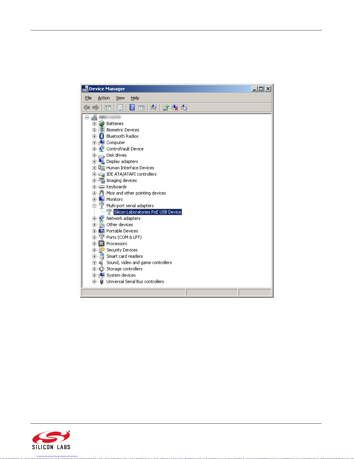
To check whether the driver is installed, open the Control Panel an d click the Device Manager icon. T he screen
shown in Figure 33 will appear. Click on “Multi-port serial adapters”, and, if it has installed, the driver will appear as
“Silicon Laboratories PoE USB Device”.
Figure 33. Device Manager
Confidential Rev. 0.1 39
Page 40

Smart.
Connected.
Energy-Friendly
Products
www.silabs.com/products
Disclaimer
Silicon Laboratories intends to provide customers with the latest, accurate, and in-depth documentation of all peripherals and modules available for system and software implementers
using or intending to use the Silicon Laboratories products. Characterization data, available modules and peripherals, memory sizes and memory addresses refer to each specific
device, and "Typical" parameters provided can and do vary in different applications. Application examples described herein are for illustrative purposes only. Silicon Laboratories
reserves the right to make changes without further notice and limitation to product information, specifications, and descriptions herein, and does not give warranties as to the accuracy
or completeness of the included information. Silicon Laboratories shall have no liability for the consequences of use of the information supplied herein. This document does not imply
or express copyright licenses granted hereunder to design or fabricate any integrated circuits. The products must not be used within any Life Support System without the specific
written consent of Silicon Laboratories. A "Life Support System" is any product or system intended to support or sustain life and/or health, which, if it fails, can be reasonably expected
to result in significant personal injury or death. Silicon Laboratories products are generally not intended for military applications. Silicon Laboratories products shall under no
circumstances be used in weapons of mass destruction including (but not limited to) nuclear, biological or chemical weapons, or missiles capable of delivering such weapons.
Trademark Information
Silicon Laboratories Inc., Silicon Laboratories, Silicon Labs, SiLabs and the Silicon Labs logo, Bluegiga, CMEMS®, EFM, EFM32, EFR, Energy Micro, Energy Micro logo and combinations thereof, "the world’s most energy friendly microcontrollers", Ember®, EZLink®, EZMac®, EZRadio®, EZRadioPRO®, DSPLL®, ISOmodem ®, Precision32®, ProSLIC®,
SiPHY®, Telegesis, USBXpress® and others are trademarks or registered trademarks of Silicon Laboratories Inc. ARM, CORTEX, Cortex-M3 and THUMB are trademarks or
registered trademarks of ARM Holdings. Keil is a registered trademark of ARM Limited. All other products or brand names mentioned herein are trademarks of their respective holders.
Silicon Laboratories Inc.
400 West Cesar Chavez
Austin, TX 78701
USA
Quality
www.silabs.com/quality
Support and Community
community.silabs.com
http://www.silabs.com
 Loading...