

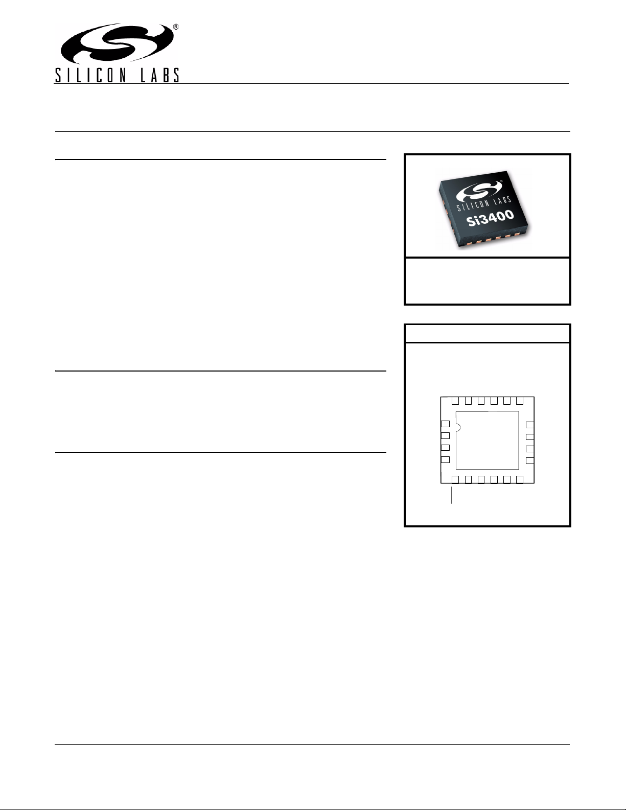
Si3400
Si3401
FULLY-INTEGRATED 802.3-COMPLIANT PD INTERFACE
AND
SWITCHING REGULATOR
Features
IEEE 802.3 standard-compliant
solution, including pre-standard
(legacy) PoE support
Highly-integrated IC enables
compact solution footprints
Minimal external components
Integrated diode bridges and
transient surge suppressor
Integrated switching regulator
controller with on-chip power
FET
Integrated dual current-limited
hotswap switch
Support non-isolated and
isolated switching topologies
Comprehensive protection
circuitry
Transient overvoltage
protection
Undervoltage lockout
Early power-loss indicator
Thermal shutdown protection
Foldback current limiting
Programmable classification
circuit
Low-profile 5 x 5 mm 20-pin QFN
Pb-Free and RoHS-compliant
Applications
Voice over IP telephones and
adapters
Wireless access points
Security cameras
Point-of-sale terminals
Internet appliances
Network devices
High power applications (Si3401)
Description
The Si3400 and Si3401 integrate all power management and control
functions required in a Power-over-Ethernet (PoE) powered device (PD)
application. The Si3400 and Si3401 convert the high voltage supplied over
the 10/100/1000BASE-T Ethernet connection into a regulated, low-voltage
output supply. The optimized architectures of the Si3400 and Si3401
minimize the solution footprint, reduce external BOM cost, and enable the
use of low-cost external components while maintaining high performance.
The Si3400 and Si3401 integrate the required diode bridges and transient
surge suppressors, thus enabling direct connection of ICs to the Ethernet
RJ-45 connector. The switching power FET and all associated functions are
also integrated. The integrated switching regulator supports isolated
(flyback) and non-isolated (buck) converter topologies. The Si3400 and
Si3401 support IEEE STD™ 802.3-2005 (future instances are referred to as
802.3) compliant solutions as well as pre-standard products, all in a single
IC. Standard external resistors connected to the Si3400 and Si3401 provide
the proper 802.3 signatures for the detection function and programming of
the classification mode. Startup circuits ensure well-controlled initial
operation of both the hotswap switch and the voltage regulator. The Si3400
and Si3401 are available in low-profile, 20-pin, 5 x 5 mm QFN packages.
While the Si3400 is designed for applications up to 10 W, the Si3401 is
optimized for higher power applications (up to approximately 15 W). See
also “AN313: Using the Si3400/01 in High Power Applications” for more
information.
Ordering Information:
See Ordering Guide on page
page 18.
Pin Assignments
5x5mm QFN
(Top View)
1
VPOSS
VSS1
SWO
VSS2
FB
1
EROUT
2
SSFT
VDD
ISOSSFT
3
2
4
VNEG
(PAD)
5678
HSO
RDET
PLOSS
Notes:
1. Pin VSSA added on revisions CZ
and higher.
2. Pin ISOSSFT added on revisions
CZ and higher. Function
available on revision E silicon.
For Rev CZ, or to disable this
feature on Revision E, tie this pin
to VDD.
VSSA
151620 19 18 17
14
13
12
11
10
9
SP2
RCL
VNEG
CT1
CT2
VPOSF
SP1
Preliminary Rev. 0.91 10/07 Copyright © 2007 by Silicon Laboratories Si3400/Si3401
This information applies to a product under development. Its characteristics and specifications are subject to change without notice.

Si3400/Si3401
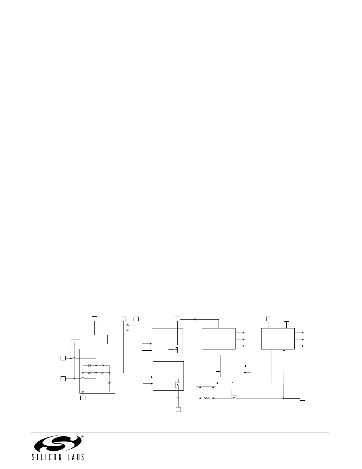
Functional Block Diagram
CT1
CT2
SP1
SP2
VPOSF
VNEG
VPOSS
&
Rectification
Protection
RDET RCL
Detection
&
Classification
Hotswap
Switch
&
Current limit
HSO
SSFT ISOSSFT
PLOSS
VDD
Hotswap
Control
&
Common
Bias
VSSA
Switcher
Control
Switching
FET
VSS1
EROUT
FB
SWO
VSS2
2 Preliminary Rev. 0.91

Si3400/Si3401
TABLE OF CONTENTS
Section Page
1. Electrical Specifications . . . . . . . . . . . . . . . . . . . . . . . . . . . . . . . . . . . . . . . . . . . . . . . . . . .4
2. Typical Application Schematics . . . . . . . . . . . . . . . . . . . . . . . . . . . . . . . . . . . . . . . . . . . . .9
3. Functional Description . . . . . . . . . . . . . . . . . . . . . . . . . . . . . . . . . . . . . . . . . . . . . . . . . . .11
3.1. Overview . . . . . . . . . . . . . . . . . . . . . . . . . . . . . . . . . . . . . . . . . . . . . . . . . . . . . . . . . .11
3.2. PD Hotswap Controller . . . . . . . . . . . . . . . . . . . . . . . . . . . . . . . . . . . . . . . . . . . . . . .11
3.3. Switching Regulator . . . . . . . . . . . . . . . . . . . . . . . . . . . . . . . . . . . . . . . . . . . . . . . . .14
4. Pin Descriptions . . . . . . . . . . . . . . . . . . . . . . . . . . . . . . . . . . . . . . . . . . . . . . . . . . . . . . . . .16
5. Package Outline . . . . . . . . . . . . . . . . . . . . . . . . . . . . . . . . . . . . . . . . . . . . . . . . . . . . . . . . .17
6. Ordering Guide . . . . . . . . . . . . . . . . . . . . . . . . . . . . . . . . . . . . . . . . . . . . . . . . . . . . . . . . . . 18
Document Change List . . . . . . . . . . . . . . . . . . . . . . . . . . . . . . . . . . . . . . . . . . . . . . . . . . . . .19
Contact Information . . . . . . . . . . . . . . . . . . . . . . . . . . . . . . . . . . . . . . . . . . . . . . . . . . . . . . . . 20
Preliminary Rev. 0.91 3

Si3400/Si3401
1. Electrical Specifications
Table 1. Recommended Operating Conditions
Description Symbol Min Typ Max Units
|CT1 – CT2| or |SP1 – SP2| VPORT 2.8 — 57 V
Ambient Operating Temperature TA –40 25 85 °C
Note: Unless otherwise noted, all voltages referenced to VNEG. All minimum and maximum specifications are guaranteed
and apply across the recommended operating conditions. Typical values apply at nominal supply voltage and ambient
temperature unless otherwise noted.
Table 2. Absolute Maximum Ratings (DC)
Type Description Rating Unit
Voltage CT1 to CT2 –60 to 60
SP1 to SP2 –60 to 60
2
VPOS
HSO –0.3 to 60
VSS1 or VSS2 –0.3 to 60
SWO –0.3 to 60
PLOSS
RDET –0.3 to 60
RCL –0.3 to 5
SSFT to VPOS
EROUT to VSS1, VSS2, or VSSA –0.3 to VDD+0.3
FB to VPOS –5 to 0.3
RIMAX to VSS1, VSS2, or VSSA –0.3 to VDD+0.3
VSS1 to VSS2 or VSSA –0.3 to 0.3
VDD to VSS1, VSS2, or VSSA –0.3 to 5
Notes:
1. Unless otherwise noted, all voltages referenced to VNEG. Permanent device damage may occur if the maximum
ratings are exceeded. Functional operation should be restricted to those conditions specified in the operational sections
to VPOS
2
2
1
–0.3 to 60
–60 to 0.3
–5 to 0.3
V
4 Preliminary Rev. 0.91
Table 2. Absolute Maximum Ratings (DC)1 (Continued)
Type Description Rating Unit
Current RCL 0 to 100
RDET 0 to 1
CT1, CT2, SP1, SP2 –400 to 400
2
VPOS
HSO 0 to 400
PLOSS
VDD 0 to 2
SWO 0 to 400
VSS1, VSS2, or VSSA –400 to 0
Si3400/Si3401
–400 to 400
mA
–0.5 to 5
Ambient
Temperature
Notes:
1. Unless otherwise noted, all voltages referenced to VNEG. Permanent device damage may occur if the maximum
ratings are exceeded. Functional operation should be restricted to those conditions specified in the operational sections
of this data sheet. Exposure to absolute maximum rating conditions for extended periods may adversely affect device
reliability.
2. VPOS is equal to VPOSF and VPOSS tied together for test condition purposes.
Storage –65 to 150
Operating –40 to 85
°C
Preliminary Rev. 0.91 5
Si3400/Si3401
Table 3. Absolute Maximum Ratings (Transient)
Transient surge defined in IEC60060 as a 1000 V impulse of either polarity applied across CT1–CT2 or SP1–SP2. The shape of
the impulse shall have a 300 ns full rise time and a 50 µs half fall time, with 201 Ω source impedance.
1
Type Description Rating Unit
Voltage CT1 to CT2 –82 to 82
SP1 to SP2 –82 to 82
2
VPOS
–0.7 to 80
HSO –0.7 to 80
V
VSS1, VSS2, or VSSA –0.7 to 80
SWO –0.7 to 80
PLOSS
to VPOS
2
–80 to 0.7
RDET –0.7 to 80
Current CT1, CT2, SP1, SP2 –5 to 5
2
VPOS
Notes:
1. Unless otherwise noted, all voltages referenced to VNEG. Permanent device damage may occur if the maximum
ratings are exceeded. Functional operation should be restricted to those conditions specified in the operational sections
of this data sheet. Exposure to absolute maximum rating conditions for extended periods may adversely affect device
reliability.
2. VPOS is equal to VPOSF and VPOSS tied together for test condition purposes.
–5 to 5
A
Table 4. Surge Immunity Ratings
1,2,3
Type Description Rating Unit
4
CDE
Cable discharge event tolerance –3.5 to 3.5 kV
ESD (System-Level) Air discharge (IEC 61000-4-2) –16.5 to 16.5 kV
Contact discharge (IEC 61000-4-2) –8 to 8 kV
ESD (CDM) JEDEC (JESD22-C101C) –1 to 1 kV
ESD (HBM) JEDEC (JESD22-A114E) –500 to 500 V
ESD (MM) JEDEC (JESD22-A115A) –100 to 100 V
Telephony Voltage
IEEE 802.3, Clause 33.5.6 175 Vp
Compatibility
Notes:
1. Permanent device damage may occur if the maximum ratings are exceeded. Functional operation should be restricted
to those conditions specified in the operational sections of this data sheet. Exposure to absolute maximum rating
conditions for extended periods may adversely affect device reliability.
2. For more information regarding system-level surge tolerance, refer to “AN315: Robust Electrical Surge Immunity for
PoE PDs through Integrated Protection”.
3. Designs must be compliant with the PCB layout and external component recommendations outlined in the Si3400/01
EVB User’s Guides and AN296.
4. J. Deatherage and D. Jones, “Multiple Factors Trigger Cable Discharge Events in Ethernet LANs,” Electronic Design
Dec. 4, 2000.
6 Preliminary Rev. 0.91

Table 5. Electrical Characteristics
Parameter Description Min Typ Max Unit
Si3400/Si3401
Detection 2.7 — 11
Classification 14 — 22
VPORT
UVLO Turn Off — — 42
UVLO Turn On 30 — 36
1
62 — 79
Input Offset Current
Diode bridge leakage
Transient Surge
VPORT < 10 V — — 10 µA
VPORT = 57 V — — 25 µA
Class 0 0 — 4
Class 1 9 — 12
IPORT Classification
2
Class 2 17 — 20
mA
Class 3 26 — 30
Class 4 36 — 44
IPORT Operating Current
3
36 V < VPORT < 57 V — 2 3.1 mA
Inrush — 130 — mA
Current Limit
Hotswap FET On-Resistance +
R
SENSE
4
Operating
350 (Si3400)
470 (Si3401)
525
550
—mA
36 V < VPORT < 57 V 0.5 — 1.4
Power loss VPORT Threshold 27 30 33 V
V
Ω
Switcher Frequency — 350 — kHz
Maximum Switcher Duty Cycle
5
ISOSSFT connected to
VDD
—50—
%
Switching FET On-Resistance 0.3 — 0.86 Ω
Regulated Feedback @ pin FB
Regulated Output Voltage Tolerance
Notes:
1. Transient surge defined in IEC60060 as a 1000 V impulse of either polarity applied to CT1–CT2 or SP1–SP2. The
shape of the impulse shall have a 300 ns full rise time and a 50 µs half fall time with 201 Ω source impedance.
2. The classification currents are guaranteed only when recommended RCLASS resistors are used, as specified in
Table 11.
3. IPORT includes full operating current of switching regulator controller.
4. The PD interface includes dual-level input current limit. At turn-on, before the HSO load capacitor is charged, the
current limit is set at the inrush level. After the capacitor has been charged within ~1.25 V of VNEG, the operating
current limit is engaged. This higher current limit remains active until the UVLO lower limit has been tripped or until the
hotswap switch is sufficiently current-limited to cause a foldback of the HSO voltage.
5. See “AN296: Using the Si3400/01 PoE PD Controller in Isolated and Non-Isolated Designs” for more information.
6. Applies to non-isolated applications only (VOUT on schematic in Figure 1).
6
6
Output voltage tolerance @
DC Avg. — 1.23 — V
–5 — 5
VOUT
Preliminary Rev. 0.91 7
%

Si3400/Si3401
Table 5. Electrical Characteristics (Continued)
Parameter Description Min Typ Max Unit
VDD accuracy @ 0.8 mA 36 V < VPORT < 57 V 4.5 — 5.5 V
Softstart charging current — 12 — µA
Thermal Shutdown Junction temperature — 160 — ºC
Thermal Shutdown Hysteresis — — 25 ºC
Notes:
1. Transient surge defined in IEC60060 as a 1000 V impulse of either polarity applied to CT1–CT2 or SP1–SP2. The
shape of the impulse shall have a 300 ns full rise time and a 50 µs half fall time with 201 Ω source impedance.
2. The classification currents are guaranteed only when recommended RCLASS resistors are used, as specified in
Table 11.
3. IPORT includes full operating current of switching regulator controller.
4. The PD interface includes dual-level input current limit. At turn-on, before the HSO load capacitor is charged, the
current limit is set at the inrush level. After the capacitor has been charged within ~1.25 V of VNEG, the operating
current limit is engaged. This higher current limit remains active until the UVLO lower limit has been tripped or until the
hotswap switch is sufficiently current-limited to cause a foldback of the HSO voltage.
5. See “AN296: Using the Si3400/01 PoE PD Controller in Isolated and Non-Isolated Designs” for more information.
6. Applies to non-isolated applications only (VOUT on schematic in Figure 1).
Table 6. Total Power Dissipation
Description Condition Min Typ Max Units
Power Dissipation VPORT = 50 V, V
Power Dissipation* VPORT = 50 V, V
=5V, 2A — 1.2 — W
OUT
= 5 V, 2 A w/ diode
OUT
—0.7— W
bridges bypassed
*Note: Silicon Laboratories recommends the on-chip diode bridges be bypassed when output power requirements are >10 W
(Si3401) or in thermally-constrained applications. For more information, see “AN313: Using the Si3400 and Si3401 in
High Power Applications”.
Table 7. Package Thermal Characteristics
Parameter Symbol Test Condition Typ Units
Thermal resistance
(junction to ambient)
θ
JA
Still air; assumes a minimum of
nine thermal vias are connected
to a 2 in
2
heat spreader plane for
the package “pad” node
(VNEG).
44 °C/W
8 Preliminary Rev. 0.91

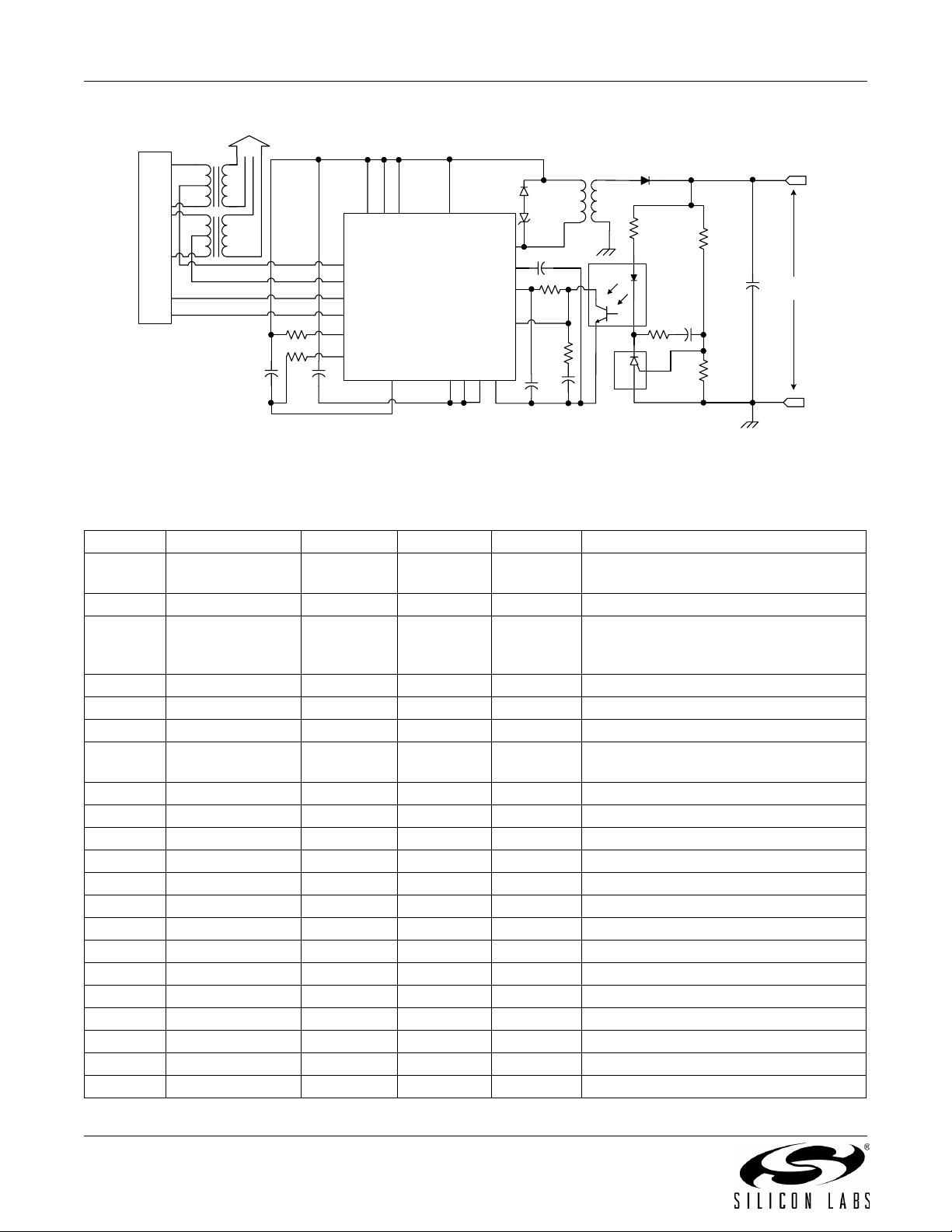
2. Typical Application Schematics
To
Ethernet PHY
Si3400/Si3401
C5
RJ-45
C2
C1
R1
CT1
CT2
SP1
SP2
RDET
RCL
VPOSF
VPOSS
VNEG
VDD
SSFT
Si3400
Si3401
PLOSS
HSO
ISOSSFT
EROUT
VSS1
FB
SWO
VSS2
C6
VSSA
R4
D1
C4
R3
C3
R2
L1
C7
Vout
Figure 1. Schematic—Class 0 with Non-Isolated 5 V Output*
*Note: This is a simplified schematic. See “AN296: Using the Si3400/01 PoE PD Controller in Isolated and Non-Isolated
Designs”
for more details and complete application schematics.
Table 8. Component Listing—Class 0 with 5 V Output
Item Type Value Toler. Rating Notes
C1 Capacitor 15 µF 20% 100 V Switcher supply capacitor. Several paral-
lel capacitors are used for lower ESR.
C2 Capacitor 0.1 µF 20% 100 V PD input supply capacitor.
C3 Capacitor 1000 µF 20% 10 V Switcher load capacitor - 1000 µF in par-
allel with and X5R 22 µF for lower ESR.
C4 Capacitor 0.1 µF 20% 16 V VDD bypass capacitor.
C5 Capacitor 0.1 µF 10% 16 V Softstart capacitor.
C6 Capacitor 3.3 nF 10% 16 V Compensation capacitor.
C7 Capacitor 150 pF 10% 16 V Compensation capacitor.
R1 Resistor 25.5 kΩ 1% 1/16 W Detection resistor.
R2 Resistor 7.32 kΩ 1% 1/16 W Feedback resistor divider.
R3 Resistor 2.87 kΩ 1% 1/16 W Feedback resistor divider.
R4 Resistor 30.1 kΩ 1% 1/16 W Feedback compensation resistor.
D1 Diode 100 V Schottky diode; part no. PDS5100.
L1 Inductor 33 µH 20% 3.5 A Coilcraft part no. DO5010333.
Preliminary Rev. 0.91 9
Si3400/Si3401
To Ethernet PHY
PS2911
D1
R5
R4
TLV431
R6
C3
C4
R7
Vout
RJ-45
D2
SWO
VDD
D3
C8
VSSA
C7
T1
R2
R3
C5
Si3400
Si3401
PLOSS
FB
HSO
ISOSSFT
EROUT
VSS2
VSS1
SSFT
VPOSF
VPOSS
CT1
CT2
SP1
R1
R8
C2
C1
SP2
RDET
RCL
VNEG
Figure 2. Schematic—Class 1 with Isolated 5.0 V Output*
*Note: This is a simplified schematic. See “AN296: Using the Si3400/01 PoE PD Controller in Isolated and Non-Isolated
Designs”
for more details and complete application schematics.
Table 9. Components—Class 1 with Isolated 5.0 V Output
Item Type Value Toler. Rating Notes
C1 Capacitor 15 µF 20% 100 V Switcher supply capacitor. Several paral-
lel capacitors are used for lower ESR.
C2 Capacitor 0.1 µF 20% 100 V PD input supply capacitor.
C3 Capacitor 1100 µF 20% 10 V Switcher load capacitor. 100 µF in paral-
lel 1000 µF and optional 1 µH inductor for
additional filtering.
C4 Capacitor 15 nF 10% 16 V Feedback compensation.
C5 Capacitor 220 nF 10% 16 V Feedback compensation.
C7 Capacitor 0.1 µF 20% 16 V VDD bypass capacitor.
C8 Capacitor 1 µF 20% 16 V Isolated mode soft start (tie ISOSSFT to
VDD if this feature is not used).
R1 Resistor 25.5 kΩ 1% 1/16 W Detection resistor.
R2 Resistor 4.99 kΩ 1% 1/16 W Pull-up resistor.
R3 Resistor 100 Ω 1% 1/16 W Feedback compensation resistor.
R4 Resistor 10 kΩ 1% 1/16 W Feedback compensation resistor.
R5 Resistor 2.05 kΩ 1% 1/16 W Pull-up resistor.
R6 Resistor 36.5 kΩ 1% 1/16 W Feedback resistor divider.
R7 Resistor 12.1 kΩ 1% 1/16 W Feedback resistor divider.
R8 Resistor 127 Ω 1% 1/16 W Classification resistor.
D1 Diode 10 A 40 V Schottky diode; part no. PN PDS1040.
D2 Diode 1 A 100 V Snubber diode (1N4148)
D3 Diode 15 V 9 A Snubber diode (DFLT15A)
T1 Transformer 40 µH Coilcraft part number FA2672 (5 V).
PS2911 Optocoupler
TLV431 Voltage reference
10 Preliminary Rev. 0.91
Si3400/Si3401
3. Functional Description
The Si3400 and Si3401 consist of two major functions:
a hotswap controller/interface and a complete pulsewidth-modulated switching regulator (controller and
power FET).
3.1. Overview
The hotswap interfaces of the Si3400 and Si3401
provide the complete front end of an 802.3-compliant
PD. The Si3400 and Si3401 also include two full diode
bridges, a transient voltage surge suppressor, detection
circuit, classification current source, and dual-level
hotswap current limiting switch. This high level of
integration enables direct connection to the RJ-45
connector, simplifies system design, and provides
significant advantages for reliability and protection. The
Si3400 and Si3401 require only four standard external
components (detection resistor, optional classification
resistor, load capacitor, and input capacitor) to create a
fully 802.3-compliant interface. For more information
about supporting higher-power applications, see
“AN313: Using the Si3400 and Si3401 in High Power
Applications” and “AN314: Power Combining Circuit for
PoE for up to 18.5 W Output”.
The Si3400 and Si3401 integrate a complete pulsewidth modulated switching regulator that includes the
controller and power FET. The switching regulator
utilizes a constant frequency pulse-width modulated
controller optimized for all possible load conditions in
PoE applications. The regulator integrates a low onresistance (Ron) switching power MOSFET that
minimizes power dissipation, increases overall regulator
efficiency, and simplifies system design. An integrated
error amplifier, precision reference, and programmable
soft-start current source provide the flexibility of using a
non-isolated buck regulator topology or an isolated
flyback regulator topology.
PLOSS
VPOSF
VPOSS
RDET
The Si3400 and Si3401 are designed to operate with
both 802.3-compliant Power Sourcing Equipment (PSE)
and pre-standard (legacy) PSEs that do not adhere to
the 802.3 specified inrush current limits. The Si3400
and Si3401 are compatible with compliant and legacy
PSEs because they use two levels for the hotswap
current limits. By setting the initial inrush current limit to
a low level, a PD based on the Si3400 or Si3401
minimizes the current drawn from either a compliant or
legacy PSE during startup. After powering up, the
Si3400 and Si3401 automatically switch to a higherlevel current limit, thereby allowing the PD to consume
up to 12.95 W (the max power allowed by the 802.3
specification).
The inrush current limit specified by the 802.3 standard
can generate high transient power dissipation in the PD.
By properly sizing the devices and implementing onchip thermal protection, the Si3400 and Si3401 can go
through multiple turn-on sequences without overheating
the package or damaging the device. The switching
regulator power MOSFET has been conservatively
designed and sized to withstand the high peak currents
created when converting a high-voltage, low-current
supply into a low-voltage, high-current supply.
Excessive power cycling or short circuit faults will
engage the thermal overload protection to prevent the
onboard power MOSFETs from exceeding their safe
and reliable operating ranges.
3.2. PD Hotswap Controller
The Si3400 and Si3401 hotswap controllers change
their mode of operation based on the input voltage
applied to the CT1 and CT2 pins or the SP1 and SP2
pins, the 802.3-defined modes of operation, and internal
controller requirements. Table 10 defines the modes of
operation for the hotswap interface.
ISOSSFT
SSFT
CT2/SP2
CT1/SP1
POWER LOSS
DETECTOR
DIODE BRIDGES
AND PROTECTION
VNEG
DETECTION
12V
0V
12V
22V
CONTROL
ON
OFF
CLASSIFICATION
CONTROL
ON
OFF
RCL
CENTRAL BIAS
BANDGAP REF
CURRENT
LIMIT
HI/LO
HOTSWAP
CONTROL
Figure 3. Hotswap Block Diagram
Preliminary Rev. 0.91 11
ON
OFF
10V
5V
1.32V
39V
32V
SWITCHER
STARTUP & BIAS
IABS
ITC
VREF
HSO

Si3400/Si3401
Table 10. Hotswap Interface Modes
Input Voltage (|CT1-
CT2| or |SP1-SP2|)
0 V to 2.7 V Inactive
2.7 V to 11 V Detection signature
11 V to 14 V Detection turns off and
14 V to 22 V Classification signature
22 V to 42 V Transition region
42 V up to 57 V Switcher operating mode
57 V down to 36 V Switcher operating mode
3.2.1. Rectification Diode Bridges and Surge Suppressor
The 802.3 specification defines the input voltage at the
RJ-45 connector of the PD with no reference to polarity.
In other words, the PD must be able to accept power of
either polarity at each of its inputs. This requirement
necessitates the use of two sets of diode bridges, one
for the CT1 and CT2 pins and one for the SP1 and SP2
pins to rectify the voltage. Furthermore, the standard
requires that a PD withstand a high-voltage transient
surge consisting of a 1000 V common-mode impulse
with 300 ns rise time and 50 µs half fall time. Typically,
the diode bridge and the surge suppressor have been
implemented externally, adding cost and complexity to
the PD system design.
The diode bridge* and the surge suppressor have been
integrated into the Si3400 and Si3401, thus reducing
system cost and design complexity.
*Note: Silicon Laboratories recommends that on-chip diode
bridges be bypassed when >10 W of output power is
required.
By integrating the diode bridges, the Si3400 and Si3401
gain access to the input side of the diode bridge.
Monitoring the voltage at the input of the diode bridges
instead of the voltage across the load capacitor
provides the earliest indication of a power loss. This true
early power loss indicator, PLOSS
microcontroller time to save states and shut down
gracefully before the load capacitor discharges below
the minimum 802.3-specified operating voltage of 36 V.
Integration of the surge suppressor enables
optimization of the clamping voltage and guarantees
protection of all connected circuitry.
Si3400 and Si3401
Mode
internal bias starts
(hysteresis limit based on
rising input voltage)
(hysteresis limit based on
falling input voltage)
, provides a local
As an added benefit, the transient surge suppressor,
when tripped, actively disables the hotswap interface
and switching regulator, preventing downstream circuits
from encountering the high-energy transients.
3.2.2. Detection
In order to identify a device as a valid PD, a PSE will
apply a voltage in the range of 2.8 V to 10 V on the
cable and look for the 25.5 kΩ signature resistor. The
Si3400 and Si3401 will react to voltages in this range by
connecting an external 25.5 kΩ resistor between VPOS
and VNEG. This external resistor and internal lowleakage control circuitry create the proper signature to
alert the PSE that a valid PD has been detected and is
ready to have power applied. The internal hotswap
switch is disabled during this time to prevent the
switching regulator and attached load circuitry from
generating errors in the detection signature.
Since the Si3400 and Si3401 integrate the diode
bridges, the IC can compensate for the voltage and
resistance effects of the diode bridges. The 802.3
specification requires that the PSE use a multi-point,
ΔV/ΔI measurement technique to remove the diodeinduced dc offset from the signature resistance
measurement. However, the specification does not
address the diode's nonlinear resistance and the error
induced in the signature resistor measurement. Since
the diode's resistance appears in series with the
signature resistor, the PD system must find some way of
compensating for this error. In systems where the diode
bridges are external, compensation is difficult and
suffers from errors. Since the diode bridges are
integrated in the Si3400 and Si3401, the IC can easily
compensate for this error by offsetting resistance across
all operating conditions and thus meeting the 802.3
requirements. An added benefit is that this function can
be tested during the IC’s automated testing step,
guaranteeing system compliance when used in the final
PD application. For more information about supporting
higher-power applications (above 12.95 W), see
“AN313: Using the Si3400 and Si3401 in High Power
Applications” and “AN314: Power Combining Circuit for
PoE for up to 18.5 W Output”.
3.2.3. Classification
Once the PSE has detected a valid PD, the PSE may
classify the PD for one of five power levels or classes. A
class is based on the expected power consumption of
the powered device. An external resistor sets the
nominal class current that can then be read by the PSE
to determine the proper power requirements of the PD.
When the PSE presents a fixed voltage between 15.5 V
and 20.5 V to the PD, the Si3400 and Si3401 assert the
class current from VPOS through the RCL resistor.
12 Preliminary Rev. 0.91

The resistor values associated with each class are
shown in Table 11.
Table 11. Class Resistor Values
Si3400/Si3401
Class Usage Power Levels Nominal Class
0 Default 0.44 W to 12.95 W < 4 mA > 1.33 kΩ
1 Optional 0.44 W to 3.84 W 10.5 mA 127 Ω
2 Optional 3.84 W to 6.49 W 18.5 mA 69.8 Ω
3 Optional 6.49 W to 12.95 W 28 mA 45.3 Ω
4 Reserved Reserved 40 mA 30.9 Ω
The 802.3 specification limits the classification time to
75 ms to limit the power dissipated in the PD. If the PSE
classification period exceeds 75 ms and the die
temperature rises above the thermal shutdown limits,
the thermal protection circuit will engage and disable
the classification current source in order to protect the
Si3400 and Si3401. The Si3400 and Si3401 stay in
classification mode until the input voltage exceeds 22 V
(the upper end of its classification operation region).
3.2.4. Under Voltage Lockout
The 802.3 standard specifies the PD to turn on when
the line voltage rises to 42 V and for the PD to turn off
when the line voltage falls to 30 V. The PD must also
maintain a large on-off hysteresis region to prevent
wiring losses between the PSE and the PD from
causing startup oscillation.
The Si3400 and Si3401 incorporate an undervoltage
lockout (UVLO) circuit to monitor the line voltage and
determine when to apply power to the integrated
switching regulator. Before the power is applied to the
switching regulator, the hotswap switch output (HSO)
pin is high-impedance and typically follows VPOS as
the input is ramped (due to the discharged switcher
supply capacitor). When the input voltage rises above
the UVLO turn-on threshold, the Si3400 and Si3401
begin to turn on the internal hotswap power MOSFET.
The switcher supply capacitor begins to charge up
under the current limit control of the Si3400 and Si3401,
and the HSO pin transitions from VPOS to VNEG. The
Si3400 and Si3401 include hysteretic UVLO circuits to
maintain power to the load until the input voltage falls
below the UVLO turn-off threshold. Once the input
voltage falls below 30 V, the internal hotswap MOSFET
is turned off.
RCL Resistor (1%,
Current
3.2.5. Dual Current Limit and Switcher Turn-On
The Si3400 and Si3401 implement dual current limits.
While the hotswap MOSFET is charging the switcher
supply capacitor, the Si3400 and Si3401 maintain a low
current limit. The switching regulator is disabled until the
voltage across the hotswap MOSFET becomes
sufficiently low, indicating the switcher supply capacitor
is almost completely charged. When this threshold is
reached, the switcher is activated, and the hotswap
current limit is increased. This threshold also has
hysteresis to prevent systemic oscillation as the
switcher begins to draw current and the current limit is
increased, which allows resistive losses in the cable to
effectively decrease the input supply.
The Si3400 and Si3401 stay in a high-level current limit
mode until the input voltage drops below the UVLO turnoff threshold or excessive power is dissipated in the
hotswap switch. This dual level current limit allows the
system designer to design powered devices for use with
both legacy and compliant PoE systems.
An additional feature of the dual current limit circuitry is
foldback current limiting in the event of a fault condition.
When the current limit is switched to the higher level,
400 mA of current can be drawn by the PD. Should a
fault cause more than this current to be consumed, the
voltage across the hotswap MOSFET will increase to
clamp the maximum amount of power consumed. The
power dissipated by the MOSFET can be very high
under this condition. If the fault is very low impedance,
the voltage across the hotswap MOSFET will continue
to rise until the lower current limit level is engaged,
further reducing the dissipated power. If the fault
condition remains, the thermal overload protection
circuitry will eventually engage and shut down the
hotswap interface and switching regulator. The foldback
current limiting occurs much faster than the thermal
overload protection and is, therefore, necessary for
comprehensive protection of the hotswap MOSFET.
1/16 W)
(or open circuit)
Preliminary Rev. 0.91 13

Si3400/Si3401
3.2.6. Power Loss Indicator
A situation can occur in which power is lost at the input
of the diode bridge and the hotswap controller does not
detect the fault due to the VPOS to VNEG capacitor
maintaining the voltage. In such a situation, the PD can
remain operational for hundreds of microseconds
despite the PSE having removed the line voltage. If it is
recognized early enough, the time from power loss to
power failure can provide valuable time to gracefully
shut down an application.
Due to integration of the diode bridges, the Si3400 and
Si3401 are able to instantaneously detect the removal
of the line voltage and provide that early warning signal
to the PD application. The PLOSS
pin is an open drain
output that pulls up to VPOS when a line voltage greater
than 27 V is applied. When the line voltage falls below
27 V, the output becomes high-impedance, allowing an
external pull-down resistor to change the logic state of
PLOSS. The benefit of this indicator is that the powered
device may include a microcontroller that can quickly
save its memory or operational state before draining the
supply capacitors and powering itself down. This feature
can help improve overall manageability in applications,
such as wireless access points.
3.3. Switching Regulator
Power over Ethernet (PoE) applications fall into two
broad categories, isolated and non-isolated. Nonisolated systems can be used when the powered device
is self-contained and does not provide external
conductors to the user or another application. Nonisolated applications include wireless access points and
FBSSFT
EROUT
VPOSF
security cameras. In these applications, there is no
explicit need for dc isolation between the switching
regulator output and the hotswap interface. An isolated
system must be used when the powered device
interfaces with other self-powered equipment or has
external conductors accessible to the user or other
applications. For proper operation, the regulated output
supply of the switching regulator must not have a dc
electrical path to the hotswap interface or switching
regulator primary side. Isolated applications include
point-of-sale terminals where the user can touch the
grounded metal chassis.
The application determines the converter topology. An
isolated application will require a flyback transformerbased switching topology while a non-isolated
application can use an inductor-based buck converter
topology. In the isolated case, dc isolation is achieved
through a transformer in the forward path and a voltage
reference plus opto-isolator in the feedback path. The
application circuit shown in Figure 2 is an example of
such a topology. The non-isolated application in
Figure 1 makes use of a single inductor as the energy
conversion element, and the feedback signal is directly
supplied into the internal error amplifier. As can be seen
from the application circuits, the isolated topology has
an increased number of components, thus increasing
the bill of materials (BOM) and system footprint.
To optimize cost and ease implementation, each
application should be evaluated for its isolated or nonisolated requirements.
VPOSS
VDD
PULSE-
WIDTH
MODULATOR
ISOSSFT
VSSA
IABS
ITC
VREF
ERROR
AMPLIFIE R
OSCILLATOR
SWITCHER
STARTUP & BIAS
HSO
Figure 4. Switcher Block Diagram
14 Preliminary Rev. 0.91
SWITCH
DRIVE
VSS1
SWO
VSS2

Si3400/Si3401
3.3.1. Switcher Startup
The switching regulator is disabled until the hotswap
interface has both identified itself to the PSE and
charged the supply capacitor needed to filter the
switching regulator's high-current transients. Once the
supply capacitor is charged, the hotswap controller
engages the internal bias currents and supplies used by
the switcher. Additionally, the soft-start current begins to
charge the external soft-start capacitor.
The voltage developed across the soft-start capacitor
serves as the error amplifier's reference in the nonisolated application. Ramping this voltage slowly allows
the switching regulator to bring up the regulated output
voltage in a controlled manner. Controlling the initial
startup of the regulated voltage restrains power
dissipation in the switching FET and prevents overshoot
and ringing in the output supply voltage.
In the isolated mode, a capacitor connected between
pins ISOSSFT and VSSA slowly ramps the duty cycle
clamp in the PWM circuit. Tie this pin to VDD if not
used.
3.3.2. Switching Regulator Operation
The switching regulator of the Si3400 and Si3401 is
constant-frequency, pulse-width-modulated (PWM), and
controller integrated with switching power FETs
optimized for the output power range defined by the
802.3 specification.
Once the hotswap interface has ensured proper turn-on
of the switching regulator controller, the switcher is fully
operational. An internal free-running oscillator and
internal precision voltage reference are fed into the
pulse-width modulator. The output of the error amplifier
(either internal for non-isolated applications or external
for isolated applications) is also routed into the PWM
and determines the slicing of the oscillator.
The PWM controls the switching FET drive circuitry. A
significant advantage of integrating the switching power
FET onto the same monolithic IC as the switching
regulator controller is the ability to precisely adjust the
drive strength and timing to the FET's sizable gate,
resulting in high regulator efficiency. Furthermore,
current-limiting circuitry prevents the switching FET
from sinking too much current, dissipating too much
power, and becoming damaged. Thermal overload
protection provides a secondary level of protection.
The flexibility of the Si3400 and Si3401's switching
regulator allows the system designer to realize either
the isolated or non-isolated application circuitry using a
single device. In operation, the integration of the
switching FET allows tighter control and more efficient
operation than a general-purpose switching regulator
coupled with a general-purpose external FET.
3.3.3. Flyback Snubber
Extremely high voltages can be generated by the
inductive kick associated with the leakage inductance of
the primary side of the flyback transformer used in
isolated applications.
Refer to “AN296: Using the Si3400/01 PoE PD
Controller in Isolated and Non-Isolated Designs” for
more information on the snubber.
Preliminary Rev. 0.91 15

Si3400/Si3401
4. Pin Descriptions
FB
VSS2
151620 19 18 17
VSSA
VPOSS
VSS1
SWO
SSFT
VDD
1
2
3
4
5678
VNEG
(PAD)
RDET
PLOSS
14
CT1
13
CT2
12
VPOSF
11
SP1
10
9
VNEG
SP2
RCL
HSO
EROUT
ISOS SFT
Table 12. Si3400 and Si3401 Pin Descriptions (Top View)
Pin# Name Description
1 EROUT Error-amplifier output and PWM input; directly connected to opto-coupler in isolated application.
2 SSFT
3 VDD 5 V supply rail for switcher; provides drive for opto-coupler.
4ISOSSFT
5
PLOSS
6RDET
7 HSO Hotswap switch output; connects to VNEG through hotswap switch.
Soft-start output pin ramps voltage across external soft-start capacitor to allow switcher to ramp
output slowly.
Isolated mode soft start enable input. Tie to VDD for non-isolated applications. Connect a
0.1 µF capacitor between this pin and VSSA for isolated applications.
Early power loss indicator; open drain output is pulled to VPOS when VPORT is applied.
Input pin for external precision detection resistor; also used for establishing absolute current reference.
8 RCL Input pin for external precision classification resistor; float if optional RCLASS is unused.
Rectified high-voltage supply, negative rail. Must be connected to thermal PAD node (VNEG)
9, Pad VNEG
on package bottom. This thermal pad must be connected to VNEG (pin #9) as well as a 2 in
heat spreader plane using a minimum of nine thermal vias.
10 SP2 High-voltage supply input from spare pair; polarity-insensitive.
11 SP1 High-voltage supply input from spare pair; polarity-insensitive.
12 VPOSF Rectified high-voltage supply, positive rail (force node)
13 CT2 High-voltage supply input from center tap of Ethernet transformer; polarity-insensitive.
14 CT1 High-voltage supply input from center tap of Ethernet transformer; polarity-insensitive.
15 VSSA Analog ground.
16 VPOSS Rectified high-voltage supply, positive rail sense node.
17 VSS1 Negative supply rail for switcher; externally tied to HSO.
18 SWO Switching transistor output; drain of switching N-FET.
19 VSS2 Negative supply rail for switcher; externally tied to HSO.
20 FB Regulated feedback input in non-isolated application.
16 Preliminary Rev. 0.91
2

Si3400/Si3401
5. Package Outline
Figure 5 illustrates the package details for the Si3400 and Si3401. Table 13 lists the values for the dimensions
shown in the illustration.
Figure 5. 20-Lead Quad Flat No-Lead Package (QFN)
Table 13. Package Dimensions
Dimension Min Nom Max
A 0.80 0.85 0.90
A1 0.00 0.02 0.05
b 0.25 0.30 0.35
D 5.00 BSC.
D2 2.60 2.70 2.80
e 0.80 BSC.
E 5.00 BSC.
E2 2.60 2.70 2.80
L 0.50 0.55 0.60
L1 0.00 — 0.10
aaa — — 0.10
bbb — — 0.10
ccc — — 0.08
ddd — — 0.10
Notes:
1. All dimensions shown are in millimeters (mm) unless otherwise noted.
2. Dimensioning and tolerancing per ANSI Y14.5M-1994.
3. This drawing conforms to the JEDEC Solid State Outline MO-220, Variation VHHB-1.
Preliminary Rev. 0.91 17

Si3400/Si3401
6. Ordering Guide
Part Number
Si3400-X-GM 20-pin QFN,
Si3401-X-GM 20-pin QFN,
Notes:
1. “X” denotes product revision.
2. Add an “R” at the end of the part number to denote tape and reel option.
3. Refer to “AN313: Using the Si3400/01 in High Power Applications” and “AN314: Power Combining Circuit for
PoE for up to 18.5 W Output” for more information about using the Si3400 and Si3401 in higher power
applications.
1,2
Pb-free; RoHS compliant
Pb-free; RoHS compliant
Package Temp Range Recommended
Maximum Output Power
–40 to 85 °C < 10 W
–40 to 85 °C 14 to 16 W
3
18 Preliminary Rev. 0.91

Si3400/Si3401
DOCUMENT CHANGE LIST
Revision 0.3 to Revision 0.4
Updated Figure 2 on page 10.
R9 now correctly connected to VNEG; RIMAX now
connects to VDD.
Added Table 7, “Package Thermal Characteristics,”
on page 8.
Updated Figure 3 on page 11.
Updated Table 5 on page 7.
Updated switcher frequency specification to 350 kHz.
Added “pad” notes to VNEG pin under Description
section in Table 12 on page 16.
Updated Table 8, “Component Listing—Class 0 with
5 V Output,” on page 9 and Table 9, “Components—
Class 1 with Isolated 5.0 V Output,” on page 10.
Updated recommended BOMs.
Revision 0.4 to Revision 0.5
Updated Table 5 on page 7.
Updated test condition for VDD current.
Updated minimum value of switcher FET on resistance.
Updated Table 9 on page 10 and Table 11 on
page 13.
Updated Rclass information.
Updated “5. Package Outline” and Table 13,
“Package Dimensions,” on page 17.
Replaced package drawing and dimensions table.
Revision 0.7 to Revision 0.8
ISOSSFT (pin 4) added throughout document.
Updated Figures 1 and 2 for addition of ISOSSFT
pin. Function available on Revision E and higher.
Revision 0.8 to Revision 0.9
Updated throughout document to support Revision
E.
Added Regulated Output Voltage Tolerance
specification to Table 5, for non-isolated applications
only.
Updated Figure 1, Figure 2, and Table 8 for Rev. E
BOM changes.
Nominal class resistor values updated for Rev. E in
Table 11.
Revision 0.9 to Revision 0.91
Updated Table 3 on page 6.
Added Table 4 on page 6.
Revision 0.5 to Revision 0.6
Added Si3401.
Updated Figure 1 on page 9.
Updated Table 8 on page 9.
Updated "6. Ordering Guide" on page 18.
Revision 0.6 to Revision 0.7
Added VSSA pin throughout document for product
revisions beginning with Rev D.
Updated Table 3 specs (for ESD).
Updated Table 5 specs (for current limits).
Updated Table 6 specs (for power dissipation).
Updated Figure 1 and Table 8.
Updated Figure 2 and Table 9.
Updated Figure 4 and Table 12.
Preliminary Rev. 0.91 19

Si3400/Si3401
CONTACT INFORMATION
Silicon Laboratories Inc.
400 West Cesar Chavez
Austin, TX 78701
Tel: 1+(512) 416-8500
Fax: 1+(512) 416-9669
Toll Free: 1+(877) 444-3032
Email: PoEinfo@silabs.com
Internet: www.silabs.com
The information in this document is believed to be accurate in all respects at the time of publication but is subject to change without notice.
Silicon Laboratories assumes no responsibility for errors and omissions, and disclaims responsibility for any consequences resulting from
the use of information included herein. Additionally, Silicon Laboratories assumes no responsibility for the functioning of undescribed features
or parameters. Silicon Laboratories reserves the right to make changes without further notice. Silicon Laboratories makes no warranty, representation or guarantee regarding the suitability of its products for any particular purpose, nor does Silicon Laboratories assume any liability
arising out of the application or use of any product or circuit, and specifically disclaims any and all liability, including without limitation consequential or incidental damages. Silicon Laboratories products are not designed, intended, or authorized for use in applications intended to
support or sustain life, or for any other application in which the failure of the Silicon Laboratories product could create a situation where personal injury or death may occur. Should Buyer purchase or use Silicon Laboratories products for any such unintended or unauthorized application, Buyer shall indemnify and hold Silicon Laboratories harmless against all claims and damages.
Silicon Laboratories and Silicon Labs are trademarks of Silicon Laboratories Inc.
Other products or brandnames mentioned herein are trademarks or registered trademarks of their respective holders.
20 Preliminary Rev. 0.91
 Loading...