Si3210/Si3211/Si3212
S
T
PROSLIC™ PROGRAMMABLE CMOS SLIC/CODEC
WITH RINGING/BATTERY VOLTAGE GENERATION
Features
Performs all BORSCHT Functi ons
Ideal for Short Loop Appl ications
(5 REN at 2 kft, 3 REN at 4 kft)
Low Voltage CMOS
Package: 38-Pin TSSOP
Compliant with Relevant LSSGR and
CCITT Specifications
Battery Voltage Generated Dynamically
with On-Chip DC-DC Converter
Controller (Si 3210 only)
5 REN Ringing Generator
Programmable Frequency, Amplitude,
Waveshape, and Cadence
Programmable AC I mpedance
A-Law/µ-Law, Linear PCM Companding
On-Hook Tr ansmission
Applications
Terminal Adaptors
Cable Telephony
PBX/Key Systems
Description
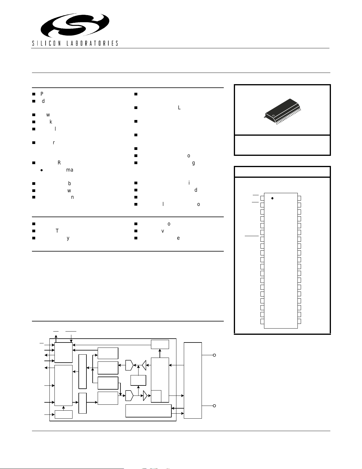
The ProSLIC™ is a low-voltage CMOS device that integrates SLIC, codec, and
battery generation functionality into a complete analog telephone interface. The
device is ideal for short loop applications such as terminal adaptors, cable telephony,
and wireless local loop. Th e ProSLIC is powered with a single 3.3 V or 5 V supply.
The Si3210 generates battery voltages dynamically usin g a software program mable
dc-dc converter from a 3.3 V to 35 V supply; negative high-voltage supplies are not
needed. All high voltage functions are performed locally with a few low cost discrete
components. The device is available in a 38- pin TSSOP and interfaces directly to
standard SPI and PCM bus digital interfaces.
Functional Block Diagram
Programmable Constant Current
Feed (20–41 mA)
Programmable Loop Closure and
Ring Trip Thresholds with Debouncing
Loop or Ground S tart Operation and
Polarity Battery Reversal
Continuous Line V olt age and Current
Monitoring
DTMF Decoder
Dual Tone Generator
SPI and PCM Bus Digital Interf aces
with Programmable Interrupt for
Control and Data
3.3 V or 5 V Operation
Multiple Loopback Modes for Testing
Pulse Metering
FSK Caller ID Generation
Wireless Local Loop
Voice Ov er IP
Integrated Access Devices
Ordering Inform ati on
See page 118.
Pin Assignments
Si3210/11/12
CS
1
INT
DRX
DTX
IREF
2
3
4
5
6
7
8
9
10
11
12
13
14
15
16
17
18
19
PCLK
FSYNC
RESET
DCH/DIO1
SDCL/DIO2
VDDA1
CAPP
QGND
CAPM
STIPDC
SRINGDC
STIPE
SVBAT
SRINGE
ProSLIC
38
37
36
35
34
33
32
31
30
29
28
27
26
25
24
23
22
21
20
SCLK
SDI
SDO
SDITHRU
DCDRV/DCSW
DCFF/DOU
TEST
GNDD
VDDD
ITIPN
ITIPP
VDDA2
IRINGP
IRINGN
IGMP
GNDA
IGMN
SRINGAC
STIPAC
RESETINT
CS
SCLK
SDO
SDI
DTX
DRX
FSYNC
PCLK
Control
Interface
PCM
Interface
PLL
CompressionExpansion
Attenuation/
Attenuation/
Si3210/11/12
DTMF
Decode
Gain/
Filter
Tone
Generator
Gain/
Filter
Line
Status
A/D
Program
Hybrid
D/A
DC-DC Converter Controller
(Si3210 only)
Line
Feed
Control
Z
S
Low Cost
External
Discretes
Patents pending
TIP
RING
Preliminary Rev. 1.11 9/ 01 Copyright © 2001 by Silicon Labora tories Si3210-DS111
This in formation applies to a product under devel opment. I ts characteristics and specifications are subject to change without notice.

Si3210/Si3211/Si3212
2 Preliminary Rev. 1.11

Si3210/Si3211/Si3212
TABLE OF CONTENTS
Section Page
Electrical Specifications . . . . . . . . . . . . . . . . . . . . . . . . . . . . . . . . . . . . . . . . . . . . . . . . . 4
Functional Description . . . . . . . . . . . . . . . . . . . . . . . . . . . . . . . . . . . . . . . . . . . . . . . . . . 21
Linefeed Interface . . . . . . . . . . . . . . . . . . . . . . . . . . . . . . . . . . . . . . . . . . . . . . . . . . . 21
Battery Voltage Generation and Switching . . . . . . . . . . . . . . . . . . . . . . . . . . . . . . . . 27
Tone Generation . . . . . . . . . . . . . . . . . . . . . . . . . . . . . . . . . . . . . . . . . . . . . . . . . . . . 30
Ringing Generation . . . . . . . . . . . . . . . . . . . . . . . . . . . . . . . . . . . . . . . . . . . . . . . . . . 33
Pulse Metering Generation . . . . . . . . . . . . . . . . . . . . . . . . . . . . . . . . . . . . . . . . . . . . 37
DTMF Detection . . . . . . . . . . . . . . . . . . . . . . . . . . . . . . . . . . . . . . . . . . . . . . . . . . . . . 38
Audio Path . . . . . . . . . . . . . . . . . . . . . . . . . . . . . . . . . . . . . . . . . . . . . . . . . . . . . . . . . 39
Two-Wire Impedance Matching . . . . . . . . . . . . . . . . . . . . . . . . . . . . . . . . . . . . . . . . . 42
Clock Generation . . . . . . . . . . . . . . . . . . . . . . . . . . . . . . . . . . . . . . . . . . . . . . . . . . . . 42
Interrupt Logic . . . . . . . . . . . . . . . . . . . . . . . . . . . . . . . . . . . . . . . . . . . . . . . . . . . . . . 42
Serial Peripheral Interface . . . . . . . . . . . . . . . . . . . . . . . . . . . . . . . . . . . . . . . . . . . . . 43
PCM Interface . . . . . . . . . . . . . . . . . . . . . . . . . . . . . . . . . . . . . . . . . . . . . . . . . . . . . . 46
Companding . . . . . . . . . . . . . . . . . . . . . . . . . . . . . . . . . . . . . . . . . . . . . . . . . . . . . . . . 47
Control Registers . . . . . . . . . . . . . . . . . . . . . . . . . . . . . . . . . . . . . . . . . . . . . . . . . . . . . . . 50
Indirect Registers . . . . . . . . . . . . . . . . . . . . . . . . . . . . . . . . . . . . . . . . . . . . . . . . . . . . . . . 108
DTMF Decoding (Si3210 and Si3211 only) . . . . . . . . . . . . . . . . . . . . . . . . . . . . . . . . 108
Oscillators . . . . . . . . . . . . . . . . . . . . . . . . . . . . . . . . . . . . . . . . . . . . . . . . . . . . . . . . . 110
Digital Programmable Gain/Attenuation . . . . . . . . . . . . . . . . . . . . . . . . . . . . . . . . . . . 111
SLIC Control . . . . . . . . . . . . . . . . . . . . . . . . . . . . . . . . . . . . . . . . . . . . . . . . . . . . . . . . 112
FSK Control . . . . . . . . . . . . . . . . . . . . . . . . . . . . . . . . . . . . . . . . . . . . . . . . . . . . . . . . 113
Pin Descriptions: Si3210/11/12 . . . . . . . . . . . . . . . . . . . . . . . . . . . . . . . . . . . . . . . . . . . . 115
Ordering Guide . . . . . . . . . . . . . . . . . . . . . . . . . . . . . . . . . . . . . . . . . . . . . . . . . . . . . . . . . 118
Package Outline: 38-Pin TSSOP . . . . . . . . . . . . . . . . . . . . . . . . . . . . . . . . . . . . . . . . . . . 119
Contact Information . . . . . . . . . . . . . . . . . . . . . . . . . . . . . . . . . . . . . . . . . . . . . . . . . . . . . 122
Preliminary Rev. 1.11 3

Si3210/Si3211/Si3212
Electrical Specifications
Table 1. Absolute Maximum Ratings and Thermal Information
*
Parameter Symbol Value Unit
DC Supply Voltage
Input Current, Digital Input Pins
Digital Input Voltage
ESD, Si3210/11/12 (Human Body Model)
Operating Temp erature Rang e
Storage Temperature Range
TSSOP-38 Thermal Resistance, Typical
*Note: Permanent device damage may occur if the above Absolute Maximum Ratings are exceeded. Functional operation
should be restricted to the conditions as specified in the operati onal sections of this data sheet. Exposure to absolute
maximum rating conditions for extende d periods may affect device reliability.
V
DDD
, V
DDA1
I
V
IND
T
T
STG
θ
IN
JA
, V
DDA2
–0.5 to 6.0 V
±10 mA
–0.3 to (V
+ 0.3) V
DDD
2000 V
A
–40 to 100 °C
–40 to 150 °C
50 °C/W
Table 2. Recommended Operating Condit ions
Parameter Symbol
Ambient Temperature T
Ambient Temperature T
Si3210/11/12 Supply Voltage V
*Note: All minimum and maximum speci fications are guara nteed and apply across the recommended operatin g conditions.
T ypical values apply at nominal supply voltag es and an operating temperature of 25
Product specifications are only guaranteed when the typical application circ uit (including compo nent tolerances) is
used.
A
A
DDD,VDDA1
,V
DDA2
Test
Condition
K-grade 0 25 70
B-grade –40 25 85
Min* Typ Max* Unit
o
C
o
C
3.13 3.3/5.0 5.25 V
o
C unless other wise stated.
4 Preliminary Rev. 1.11

Si3210/Si3211/Si3212
Table 3. AC Characteristics
(V
, V
DDA
Paramete r Test Condi t ion Min Typ Max Unit
= 3.13 to 5.25 V, TA = 0 to 70°C for K-Grade, –40 to 85°C for B-Grade)
DDD
TX/RX Performance
Overload Level THD = 1.5% 2.5 — — V
Single Frequency Distortion
1
2-wire – PCM or
— — –45 dB
PCM – 2-wire:
200 Hz–3.4 kHz
Signal-to-(Noise + Distortion) Ratio
2
200Hz to 3.4kHz
Figure 1 — —
D/A or A/D 8-bit
Active off-hook, and OHT,
any ZAC
Audio Tone Gene rator
Signal-to-Distortion Ratio
2
0 dBm0, Active off-hook,
and OHT , any Zac
45 — — dB
Intermodulation Distortion — — –41 dB
Gain Accuracy
2
2-wire to PCM, 1014 Hz –0.5 0 0.5 dB
PCM to 2-wire, 1014 Hz –0.5 0 0.5 dB
Gain Accuracy Over Frequency Figure 3,4 — —
Group Delay Over Frequency Figure 5,6 — —
Gain Tracking
3
1014 Hz sine wave, refer-
ence level –10 dBm
signal level:
3 dB to –37 dB –0.25 — 0.25 dB
–37 dB to –50 dB –0.5 — 0. 5 dB
–50 dB to –60 dB –1.0 — 1. 0 dB
PK
Round-Trip Group Delay at 1000 Hz — 1100 — µs
Gain Step Accuracy –6 dB to 6 dB –0.017 — 0.017 dB
Gain Variation with Temperature All gain settings –0.25 — 0.25 dB
Gain Variation with Supply V
DDA
= V
3.3/5 V ± 5% –0.1 — 0.1 dB
DDA =
2-Wire Return Loss 2 00 Hz to 3.4 kHz 30 35 — dB
Transhybrid Balance 300 Hz to 3.4 kHz 30 — — dB
Noise Performance
Idle Channel Noise
4
C-Message Weighted — — 15 dBrnC
Psophometric Weighted — — –75 dBmP
3 kHz flat — — 18 dBrn
PSRR from VDDA RX and TX, DC to 3.4 kHz 40 — — dB
PSRR from VDDD RX and TX, DC to 3.4 kHz 40 — — dB
PSRR from VBAT RX and TX, DC to 3.4 kHz 40 — — dB
Preliminary Rev. 1.11 5

Si3210/Si3211/Si3212
Table 3. AC Characteristics (Continued)
(V
, V
DDA
Paramete r Test Condi t ion Min Typ Max Unit
= 3.13 to 5.25 V, TA = 0 to 70°C for K-Grade, –40 to 85°C for B-Grade)
DDD
Longitudinal Performance
Longitudinal to Metallic or PCM
Balance
200 Hz to 3.4 kHz, β
150, 1% mismatch
β
= 60 to 240
Q1,Q2
β
= 300 to 800
Q1,Q2
Q1,Q2
5
5
≥
56 60 — dB
43 60 — dB
53 60 — dB
Metallic to Lon g it u din al Balanc e 200 Hz t o 3.4 k H z 40 — — dB
Longitudinal Impedance 200 Hz to 3.4 kHz at TIP or
RING
Register selectable
ETBO/ETBA
00
01
10
—
—
—
33
17
17
—
—
—
Ω
Ω
Ω
Longitudinal Current per Pin Active off-hook
200 Hz to 3.4 kHz
Register selectable
ETBO/ETBA
00
01
10
Notes:
1. The input signal level should be 0 dBm0 for frequencies greater than 100 Hz. For 100 Hz and below, the level should be
–10 dBm0. The output signal magnitude at any other frequency will be smaller than the maximum value specified.
2. Analog signal measured as V
3. The quantization errors inherent in the µ/A-law companding process can generate slightly worse gain tracking performance
in the signal range of 3 dB to –37 dB for signal frequencies that are integer divisors of the 8 kHz PCM sampling rate.
4. The level of any unwanted tones within the bandwidth of 0 to 4 kHz does not exceed –55 dBm.
5. Assumes normal distribution of betas.
TIP
– V
. Assumes ideal line impedance matching.
RING
—
—
—
4
8
8
—
—
—
mA
mA
mA
6 Preliminary Rev. 1.11
Si3210/Si3211/Si3212
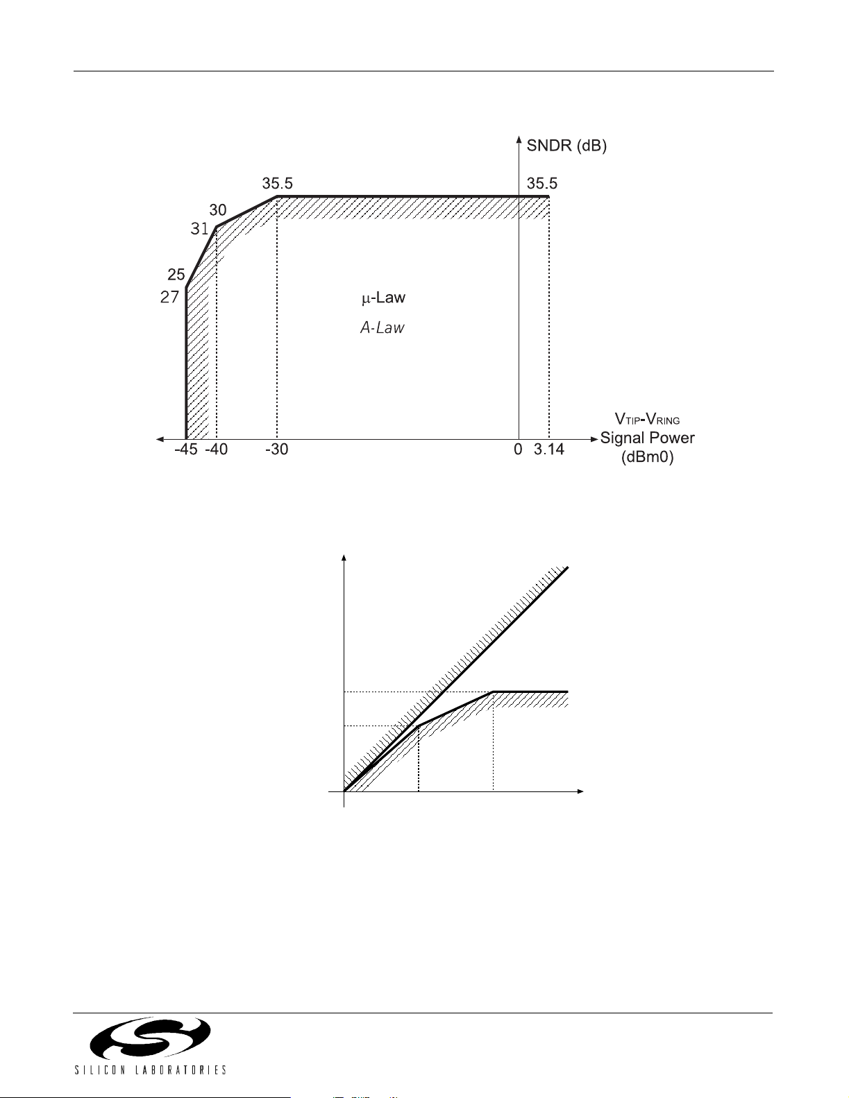
Figure 1. Transmit and Receive Path SNDR
9
8
7
6
Fundamental
Output Power
(dBm0)
5
4
3
2.6
2
1
123456789
0
Fundamental Input Power (dBm0)
Acceptable
Region
Figure 2. Overload Compression Performance
Preliminary Rev. 1.11 7
Si3210/Si3211/Si3212
Typical Response
Typical R esponse
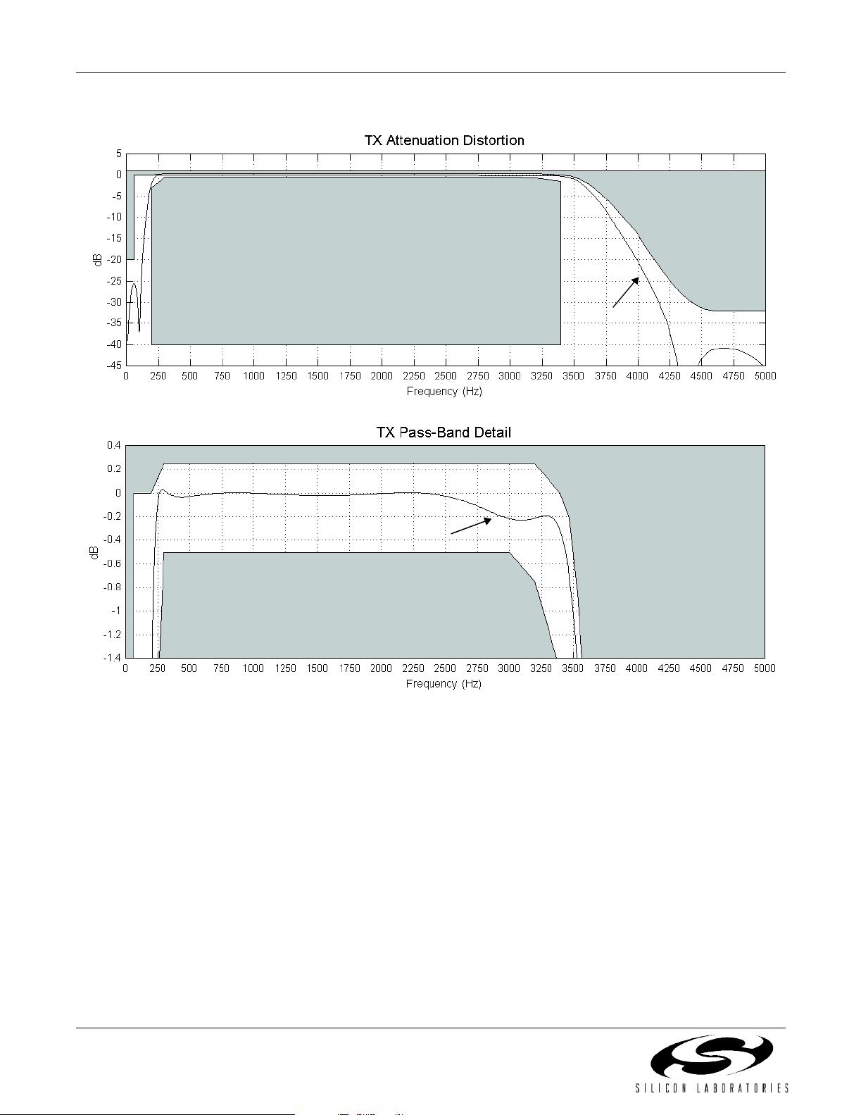
Figure 3. Transmit Path Frequency Response
8 Preliminary Rev. 1.11
Si3210/Si3211/Si3212
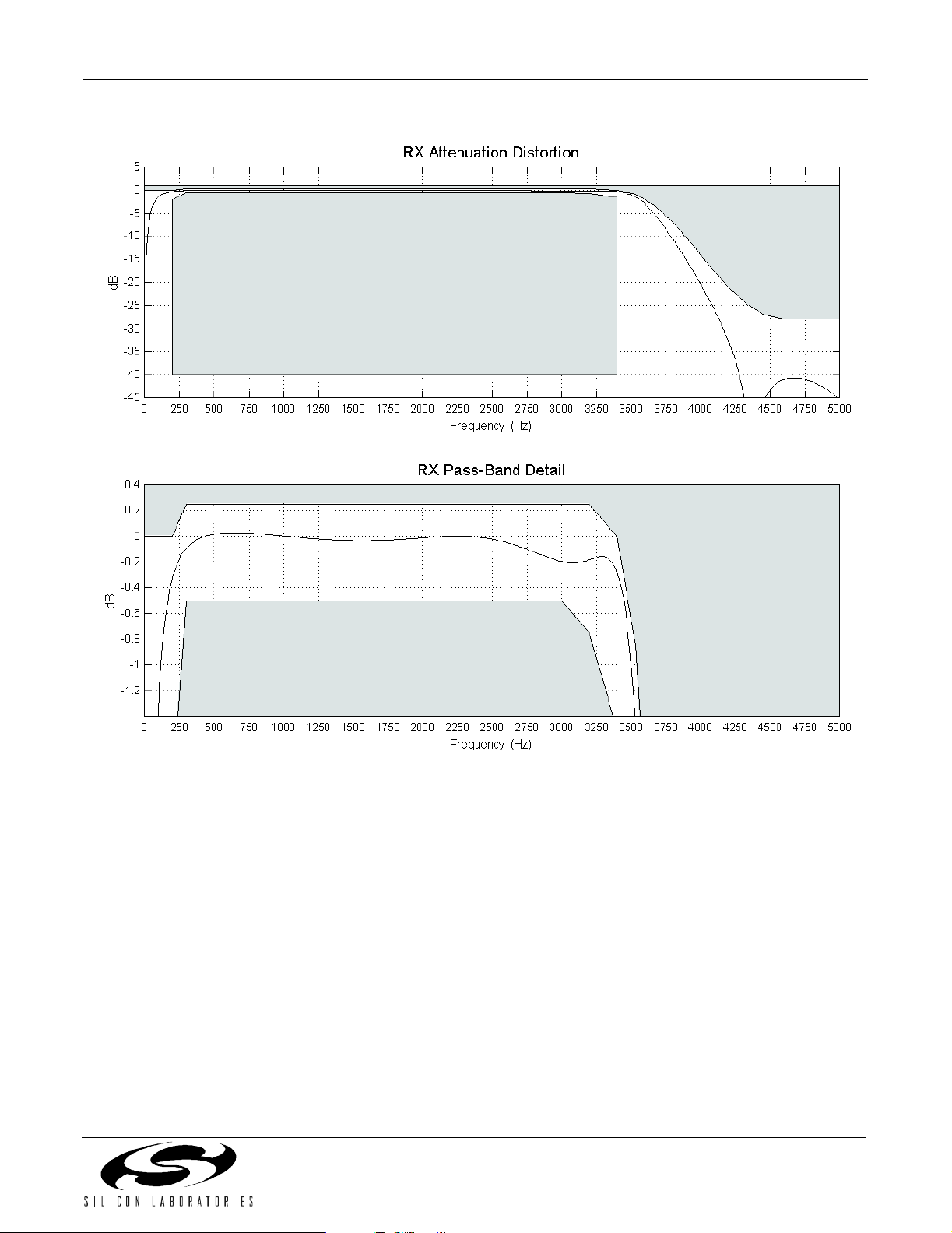
Figure 4. Receive Path Frequency Response
Preliminary Rev. 1.11 9
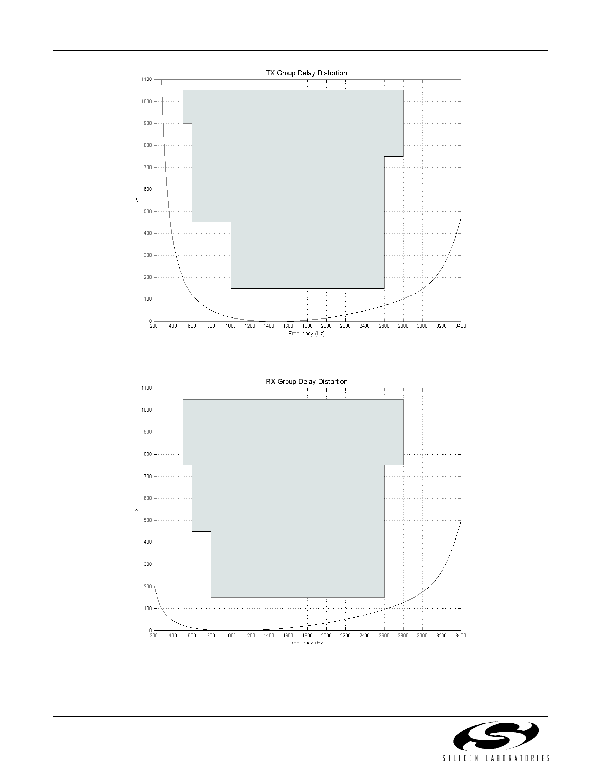
Si3210/Si3211/Si3212
Figure 5. Transmit Group Delay Distortion
Figure 6. Receive Group Delay Distortion
10 Preliminary Rev. 1.11

Si3210/Si3211/Si3212
Table 4. Linefeed Characteristics
(V
, V
DDA
Parameter Symbol Test Condition Min Typ Max Unit
= 3.13 to 5.25 V, TA = 0 to 70°C for K-Grade, –40 to 85°C for B-Grade)
DDD
Loop Resistance Range R
LOOP
DC Loop Current Accuracy I
DC Open Circuit Voltage
Accuracy
DC Differential Output
R
DO
LIM
Active Mode; V
See note.* 0 — 16 0 Ω
= 29 mA, ETBA = 4 mA –10 — 10 %
= 48 V,
– V
< I
OC
RING
LIM
V
TIP
I
LOOP
Resistance
DC Open Circuit Voltage—
Ground Start
DC Output Resistance—
V
OCTO
R
ROTO
I
RING<ILIM
I
RING<ILIM
; V
V
OC
wrt ground
RING
= 48 V
; RING to ground — 160 — Ω
Ground Start
DC Output Resistance—
R
TOTO
TIP to ground 150 — — kΩ
Ground Start
Loop Closure/Ring Ground
I
= 11.43 mA –20 — 20 %
THR
Detect Threshold Accuracy
Ring Trip Threshold
R
= 11 00 Ω –20 — 20 %
THR
Accuracy
Ring Trip Response Time User Programmable Register 70
and Indir ect Register 36
Ring Amplitude V
Ring DC Offset R
TR
OS
5 REN load; sine wave;
R
LOOP
= 160 Ω, V
BAT
= –75 V
Programmable in Indirect
Register 19
–4 — 4 V
—160— Ω
–4 — 4 V
———
44 — — V
RMS
0——V
Trapezoidal Ring Crest
Crest factor = 1.3 – .05 — .05
Factor Accuracy
Sinusoidal Ring Crest
R
CF
1.35 — 1.45
Factor
Ringing Frequency Accuracy f = 20 Hz –1 — 1 %
Ringing Cadence Accuracy Accuracy of ON/OFF Times –50 — 50 msec
Calibration Time ↑CAL to ↓CAL Bit — — 600 msec
Power Alarm Threshold
At Power Threshold = 300 mW –25 — 25 %
Accuracy
*Note: DC resistance round trip; 160 Ω corresponds to 2 kft 26 gauge AWG.
Preliminary Rev. 1.11 11

Si3210/Si3211/Si3212
Table 5. Monitor AD C Character i sti cs
(V
, V
DDA
Parameter Symbol Test Condition Min Typ Max Unit
= 3.13 to 5.25 V, TA = 0 to 70°C for K-Grade, –40 to 85°C for B-Grade)
DDD
Differential Nonlinearity
DNLE –1/2 — 1/2 LSB
(6-bit resolution)
Integral Nonlinearity
INLE –1 — 1 LSB
(6-bit resolution)
Gain Error (voltage) — — 10 %
Gain Error (current) — — 20 %
Table 6. Si321x DC Characteristics, V
(V
DDA,VDDD
= 4.75 V to 5.25 V, TA = 0 to 70°C for K-Grade, –40 to 85°C for B-Grade)
DDA
= V
DDD
= 5.0 V
Parameter S ymb ol Test Condition Min Typ Max Unit
High Level Input Voltage V
Low Level Input Volt age V
High Level Output Voltage V
Low Level Output Voltage V
IH
IL
DIO1,DIO2,SDITHRU:IO = –4 mA
OH
OL
SDO, DTX:I
DOUT: IO = –40 mA
DIO1,DIO2,DOUT,SDITHRU:
I
= 4 mA
O
SDO,INT
,DTX:IO = 8 mA
= –8 mA
O
0.7 V
DDD
— — 0.3 V
V
– 0.6 — — V
DDD
V
– 0.8 — — V
DDD
——0.4V
——V
DDD
V
Input Leakage Current I
L
Table 7. Si321x DC Characteristics, V
(V
DDA,VDDD
= 3.13 V to 3.47 V , TA = 0 to 70°C for K-Grade, –40 to 85°C for B-Grade)
DDA
= V
DDD
= 3.3 V
–10 — 10 µA
Parameter Symbol Test Condition Min Typ Max Unit
High Level Input Voltage V
Low Level Input Voltage V
High Level Output Voltage V
Low Level Output Voltage V
Input Leakage Current I
IH
IL
OH
OL
L
DIO1,DIO2,SDITHRU:IO = –2 mA
SDO, DTX:I
DOUT: IO = –40 mA
DIO1,DIO2,DOUT,SDITHRU:
SDO,INT
= –4 mA
O
I
= 2 mA
O
,DTX:IO = 4 mA
0.7 V
DDD
— — 0.3 V
V
– 0.6 — — V
DDD
V
– 0.8 — — V
DDD
——0.4V
–10 — 10 µA
—— V
DDD
V
12 Preliminary Rev. 1.11

Table 8. Power Supply Characteristics
(V
DDA,VDDD
= 3.13 V to 5.25 V, TA = 0 to 70°C for K-Grade, –40 to 85°C for B-Grade)
Si3210/Si3211/Si3212
Parameter
Power Supply Current,
Analog and Digital
Power Supply Current, V
BAT
Symbol Test Condi t io n
+ I
I
A
D
Sleep (RESET = 0) 0.1 0.25 0.42 mA
Open 33 42.8 49 m A
Active on-hook
ETBO = 4 mA
Active OHT
ETBO = 4 mA 57 72 83 mA
Active off-hook
ETBA = 4 mA, I
Ground-start 36 47 55 mA
Ringing
Sinewave, REN = 1, V
3
I
BAT
Sleep (RESET = 0) — 0 — m A
Open (DCOF = 1) — 0 — mA
Active on-hook
= 48 V, ETBO = 4 mA — 3 —
V
OC
Active OHT
ETBO = 4 mA — 11 —
1
Typ
Typ
46 57 68 mA
= 20 mA 73 88 9 9
LIM
= 56 V 45 55 65
PK
2
Max Unit
mA
mA
mA
mA
Active off-hook
ETBA = 4 mA, I
= 20 mA — 30 —
LIM
mA
Ground-start — 2 — m A
Ringing
V
PK_RING
= 56 VPK,
—5.5—
mA
sinewave ringing, REN = 1
Notes:
1. V
2. V
3. I
, V
, V
DDA
DDA
= 3.3 V.
= 5.25 V.
(the large negative supply). For a switched-mode power supply regulator efficiency of 71%,
BAT
DDD
DDD
= current from V
BAT
the user can calculate the regulator current consumption as I
BAT
V
BAT
/(0.71 VDC).
Table 9. Switching Characteristics—General Inputs
V
= V
DDA
Parameter Symbol Min Typ Max Unit
Rise Time, RESET
RESET
Note: All timing (except Rise and Fall time) is referenced to the 50% level of the waveform. In put t est levels are VIH = VD –
= 3.13 to 5.25 V, TA = 0 to 70°C for K-Grade, –40 to 85°C for B-Grade, CL = 20 pF)
DDA
Pulse W i dt h t
0.4 V, V
= 0.4 V. Rise and Fall times are refer enced to the 20% and 80% levels of the waveform.
IL
t
r
rl
— — 20 ns
100 — — ns
Preliminary Rev. 1.11 13
Si3210/Si3211/Si3212
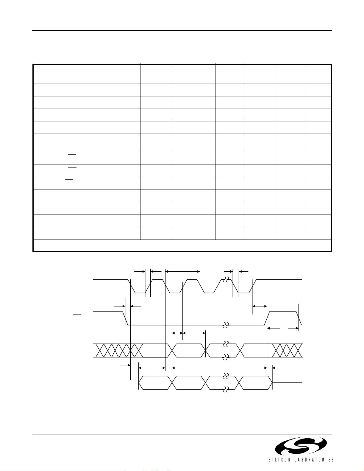
Table 10. Switching Characteristics—SPI
V
DDA
= V
= 3.13 to 5.25 V, TA = 0 to 70°C for K-Grade, –40 to 85°C for B-Grade, CL = 20 pF
DDA
Parameter
Symbol
Cycle Time SCLK t
Rise Time, SCLK t
Fall Time, SCL K t
Delay Time, SCL K Fall to SDO Active t
Delay Time, SCL K Fall to SDO
Transition
Delay Time, CS
Setup Time, CS
Hold Time, CS
Rise to SDO Tri-state t
to SCLK Fall t
to SCLK Rise t
Setu p Time, SD I to SCL K Rise t
Hold Time, SDI to SCLK Rise t
Delay Time between Chip Selects t
SDI to SDITHRU Propagation Delay t
d1
t
d2
d3
su1
h1
su2
h2
cs
cs
Test
Conditions
c
r
f
Min Typ Max Unit
0.062 — — µsec
— — 25 ns
— — 25 ns
— — 20 ns
— — 20 ns
— — 20 ns
25 — — ns
20 — — ns
25 — — ns
20 — — ns
220 — — ns
—4—ns
Note: All timing is referenced to the 50% level of the waveform. Input test levels are V
t
t
r
thru
t
c
SCLK
t
su1
CS
t
t
su2
h2
SDI
t
d1
t
d2
SDO
Figure 7. SPI Timing Diagram
IH
= V
–0.4 V, VIL = 0.4 V
DDD
t
r
t
h1
t
cs
t
d3
14 Preliminary Rev. 1.11
Si3210/Si3211/Si3212
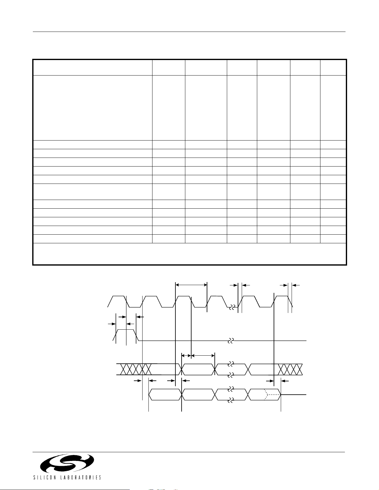
Table 11. Switchi n g C h ar acteristic s—PCM H igh way Seri al I n ter face
VD = 3.13 to 5.25 V, TA = 0 to 70°C for K-Grade, –40 to 85°C for B-Grade, CL = 20 pF
Parameter
Symbol
PCLK Frequency 1/t
PCLK Duty Cycle Tolerance t
PCLK Period Jitter Tolerance t
jitter
Rise Time, PCLK t
Fall Time, PCL K t
Delay Time, PCLK Rise to DTX Active t
Delay Time, PCLK Rise to DTX
t
c
dty
r
f
d1
d2
Test
Conditions
Transition
Delay Time, PCLK Rise to DTX Tri-state
Setup Time, FSYNC to PCLK Fall t
Hold Time, FSYNC to PCLK Fall t
Setup Time, DRX to PCLK Fall t
Hold Time, DRX to PCLK Fall t
Notes:
1. All timing is ref erenced to the 50% level of the waveform. Input test levels are V
2. Spec applies to PCLK fall to DTX tri-state when th at mode is selected (TRI = 0).
2
t
d3
su1
h1
su2
h2
Min
—
—
—
—
—
—
—
—
1
Typ
0.256
0.512
0.768
1.024
1.536
2.048
4.096
8.192
1
Max
—
—
—
—
—
—
—
—
1
Units
MHz
MHz
MHz
MHz
MHz
MHz
MHz
MHz
40 50 60 %
–120 — 120 ns
— — 25 ns
— — 25 ns
— — 20 ns
— — 20 ns
— — 20 ns
25 — — ns
20 — — ns
25 — — ns
20 — — ns
IH – VI/O –
0.4V, VIL = 0.4V
PCLK
FSYNC
DRX
DTX
t
r
t
su1
t
c
t
h1
t
su2th2
t
d1
t
d2
Figure 8. PCM Highway Interface Timing Diagram
t
f
t
d3
Preliminary Rev. 1.11 15
Si3210/Si3211/Si3212
0
F
220nF
Q4
5401
R10
10
C8
R13
5.1k
Q2
5401
R11
10
Q5
5551
C7
220nF
R7
80.6
C26
0.1uF
R21
15
Q9
2N2222
1
1
R28
R29
Note 1
Q1
5401
TIP
Protection
Circuit
22nF
22nF
Q6
5551
C5
C6
RING
Notes:
1. Values and configurations for these
components can be derived from Table 19
or from App Note 45.
2. Only one component per system needed.
3. All circuit grounds should have a singlepoint connection to the ground plane.
R6
80.6
GND
5401
GND
VCC
GND
3123102730
32
TEST
R1
200k
15
20
R8
C3
470
220nF
28
29
17
R2
200k
220nF
26
25
R4
200k
19
R5
200k
18
C4
R9
470
21
16
R3
200k
Q3
R12
5.1k
VCC
GNDD
STIPDC
STIPAC
ITIPP
ITIPN
STIPE
IRINGP
IRINGN
SRINGE
SVBAT
SRINGAC
SRINGDC
SDCL
SDCH
9
8
SDCL
SDCH
DC-DC Converter
VBAT VDC
Circuit
GNDA
Si3210/Si3210M
DCDRV
34
DCDRV
VDDD
VDDA2
VDDA1
DCFF
33
DCFF
SCLK
SDI
SDO
FSYNC
PCLK
DRX
DTX
INT
RESET
IGMP
IGMN
IREF
CAPP
CAPM
QGND
VDC
38
37
36
1
CS
6
3
4
5
2
7
24
22
11
12
14
13
VDDA1
C15
0.1uF
R15
243
C2
10uFC110uF
C16
0.1uF
SPI Bus
PCM Bus
VCC
2
R32
10k
Note 2
2
R26
40.2k
R14
40.2k
VDDA2 VDDD
C17
0.1uF
C3
10u
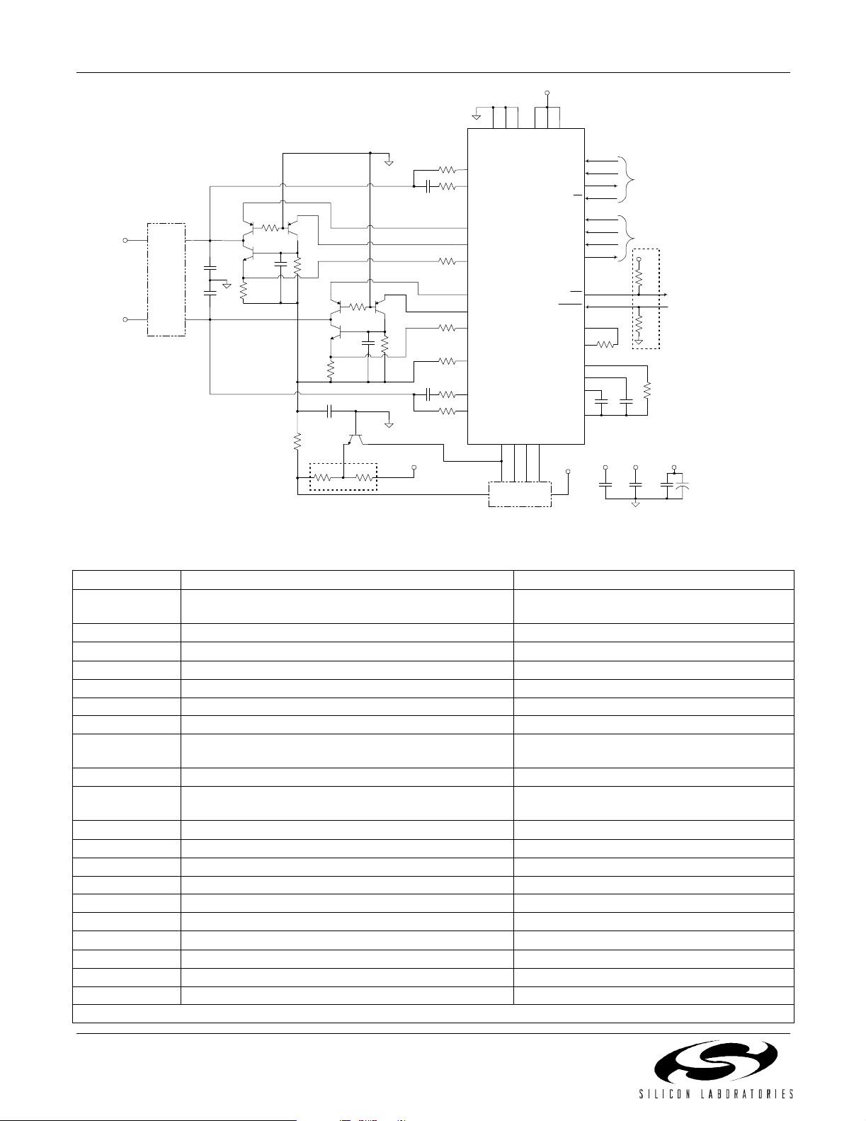
Figure 9. Si3210/Si3210M Typical Application Circuit Using Integrated DC-DC Converter
Table 12. Si3210/Si3210M External Component Values
Compon ent Value Suppl ier/Part Number
C1,C2 10 µF, 6 V Ceramic/Tantalum or 16 V Low Leakage Elec-
trolytic, ±20%
C3,C4 220 nF, 100 V, X7R, ±20% Murata, Johanson, Novacap, Venkel
C5,C6 22 nF, 100 V, X7R, ±20% Murata, Johanson, Novacap, Venkel
C7,C8 220 nF , 50 V, X7R, ±20% Murata, Johanson, Novacap, Venkel
C15,C16,C17 0.1 µF, 6 V, Y5V, ±20% Murata, Johanson, Novacap, Venkel
C26 0.1 µF, 100 V, X7R, ±20% Murata, Johanson, Novacap, Venkel
C30 10 µF, 16 V , Electrolytic, ±20% Panasonic
Q1,Q2,Q3,Q4 100 V, PNP, BJT Central Semi CMPT5 401; ON Semi
Q5,Q6 100 V, NPN, BJT Cent ral Semi CZT5551, ON Semi 2N5551
Q9 NPN General Purpose BJT ON Semi MMBT2222ALT1, MPS2222A; Cent ral
R1,R2,R3,R4,R5 200 kΩ, 1/10 W , ±1%
R6,R7 80.6 Ω, 1/4 W, ±1%
R8,R9 470 Ω, 1/10 W, ±1%
R10,R11 10 Ω, 1/10 W, ±5%
R12,R13 5.1 kΩ, 1/10 W, ±5%
R14,R26* 40.2 kΩ, 1/10 W, ±1%
R15 243 Ω, 1/ 1 0 W, ±1%
R21 15 Ω, 1/4 W, ±1%
R28,R29 1/10 W, ±1% (See AN45 or Table 17 for value selection)
R32* 10 kΩ, 1/10 W, ±5%
*Note: Only one component per system needed.
Murata, Panasonic, Nichicon URL16100MD,
Panasonic Z Series
MMBT5401LT1, 2N5401; Zetex FMMT5401
Semi CMPT2222A; Zetex FMMT2222
16 Preliminary Rev. 1.11
Si3210/Si3211/Si3212
T
VDC
F1
SDCH
SDCL
Si3210
DCFF
DCDRV
Notes:
1. Values and configurations for these components can be derived
from Table 21 or from App Note 45.
2. Voltage rating for C14 and C25 must be greater than VDC.
C10
22nF
1
R19
Note 1
1
R20
R16
200
R18
Q8
2N2222
R17
Note 1
L1
1
Q8
FZT953
D1
ES1D
C25
10uF
2
GND
10uF
2
C14
0.1uF
VBA
C9
Figure 10. Si3210 BJT/Induc tor DC-DC Converter Circuit
T a ble 13. Si3210 BJT/Inductor DC-DC Converter Component Values
Component (s) Value Supplier
C9 10 µF, 100 V, Electrolytic, ±20% Panasonic
C10 22 nF, 50 V, X7R, ±20% Murata, Johanson, Novacap, Venkel
C14* 0.1 µF, X7R, ±20% Murata, Johanson, Novacap, V enkel
C25* 10µF, Electrolytic, ±20% Panasonic
R16 200 Ω, 1/10 W, ±5%
R17 1/10 W, ±5% (See AN45 or Table 19 for value selecti on)
R18 1/4 W, ±5% (See AN45 or Table 19 for value selection)
R19,R20 1/10 W, ±1% (See AN45 or Table 19 for value selection)
F1 Fuse Belfuse SSQ Series
D1 Ultra Fast Recovery 200V, 1A Rectifier General Semi ES1D; Central Semi
CMR1U-02
L1 1A, Shielded Inductor (See AN45
Table 19 for value selecti on)
Q7 120 V, High Current Switching PNP Zetex FZT95 3, FZT955, ZTX953,
Q8 60 V, General Purpose Swit ching NPN ON Semi MMBT2222ALT1, MPS2222A;
*Note: Voltage rating of thi s device must be greater than V
DC
or
.
API Delevan SPD127 series, Sumida
CDRH127 series, Datatro nics DR340-1
series, Coilcraft DS5022, TDK
SLF12565
ZTX955
Central Semi CMPT2222A; Zetex
FMMT2222
Preliminary Rev. 1.11 17
Si3210/Si3211/Si3212
T
VDC
F1
SDCH
SDCL
C27
Si3210M
DCFF
DCDRV
Notes:
1. Values and configurations for these components can be derived
2. Voltage rating for C14 and C25 must be greater than VDC.
470pF
R17
200k
NC
from Table 20 or from App Note 45.
R19
Note 1
R20
M1
IRLL014N
R22
1
2
1
R18
1
22
Note 1
C25
10uF
1
2
D1
ES1D
3
6
4
10
1
T1
GND
C9
10uF
C14
0.1uF
2
VBA
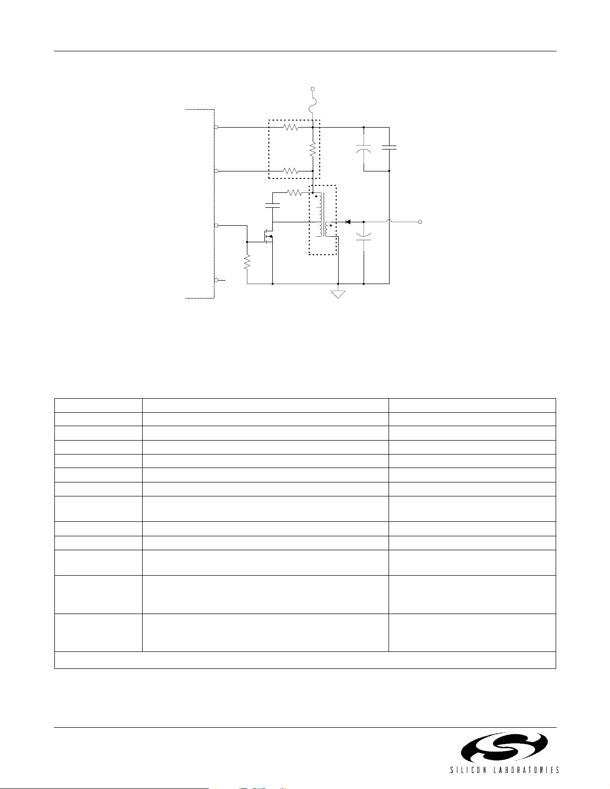
Figure 11. Si3210M MOSFET/Transformer DC-DC Converter Circuit
Table 14. Si3210M MOSFET/Transformer DC-DC Converter Component Values
Component (s) Value Supplier
C9 10 µF, 100 V, El ec trolyt ic , ±20% Panas onic
C14* 0.1
C25* 10
C27 470 pF, 100 V, X7R, ±20% Murata, Johanson, Novacap, Venkel
R17 200 k
R18 1/4 W, ±5% (See AN45 or Table 18 for value selection)
R19,R20 1/10 W , ± 1% (See AN45 or Table 18
R22 22
F1 Fuse Belfuse SSQ Series
D1 Ultra Fast Recovery 200 V, 1A Rectifier General Semi ES1D; Central Sem i
T1 Power Transformer Coiltronic CTX01-15275;
M1 100 V, Logic Level Input MOSFET Intl Rect. IRLL014N; Intersil
*Note: V oltage rating of this device must be greater t han VDC.
µF, X7R, ±20% Murata, Johanson, Novacap, Venkel
µF, Electrolytic, ±20% Panasonic
Ω, 1/10 W, ± 5%
for value selection)
Ω, 1/10 W, ±5%
CMR1U-02
Datatronics SM76315;
Midcom 31353R-02
HUF76609D3S; ST Micro
STD5NE10L, STN2NE10L
18 Preliminary Rev. 1.11
Q1
5401
TIP
Protection
Circuit
22nF
22nF
C5
C6
5551
Q6
R6
80.6
RING
Notes:
1. Only one component per system needed.
2. All circuit grounds should hav e a singl e-point
connection to the ground plane.
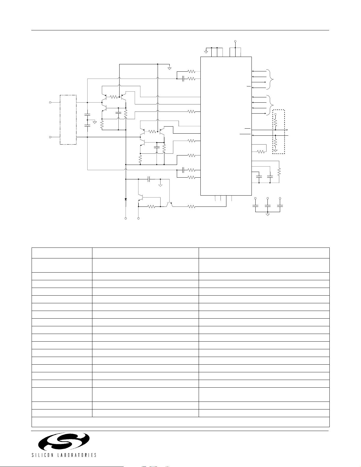
Figure 12. Si3211/12 Typical Application Circuit Using Extended Battery
C8
220nF
Si3210/Si3211/Si3212
VCC
3123102730
32
R1
C3
220nF
220nF
200k
R8
470
R2
200k
R4
200k
R5
200k
C4
R9
470
R3
200k
R18
1.8k
GND
Q4
5401
R10
10
R13
5.1k
C7
C9
R16
200k
Q3
5401
R11
10
R12
5.1k
GND
Q7
5401
VBATL
4003
Q2
5401
Q5
5551
220nF
R7
80.6
0.1uF
Q8
5551
D1
VBATH
15
STIPDC
20
STIPAC
28
ITIPP
29
ITIPN
17
STIPE
26
IRINGP
25
IRINGN
19
SRINGE
18
SVBAT
21
SRINGAC
16
SRINGDC
TEST
GNDA
GNDD
Si3211/Si3212
DIO2
DIO1
DCSW
9
8
34
NC NC NC
VDDD
VDDA2
VDDA1
DOUT
33
SCLK
SDI
SDO
FSYNC
PCLK
DRX
DTX
INT
RESET
IGMP
IGMN
IREF
CAPP
CAPM
QGND
CS
C15
0.1uF
38
37
36
1
6
3
4
5
2
7
24
R15
243
22
11
12
C2
14
13
C1
10uF
10uF
VDDA1 VDDA2 VDDD
C17
C16
0.1uF
0.1uF
SPI Bus
PCM Bus
VCC
1
R32
10k
Note 1
1
R26
40.2k
R14
40.2k
Table 15. Si3211/12 External Component Values
Component Value Supplier/Part Number
C1,C2 10 µF, 6 V Ceramic/Tantalum or 16 V Low
Leakage Electrolytic, ±20%
C3,C4 220 nF, 100 V, X7R, ±20% Murata, Johanson, Novacap, Venkel
C5,C6 22 nF , 100 V, X7R, ±20% Murata, Johanson, Novacap, Venkel
C7,C8 220 nF, 50 V, X7R, ±20% Murata, Johanson, Novacap, Venkel
C9 0.1 µF, 100 V, Electrolytic, ±20% Panasonic
C15,C16,C17 0.1 µF, 6 V, Y5V, ±20% Murata, Johanson, Novacap, Venkel
R1,R2,R3,R4,R5,R16 200 kΩ, 1/1 0 W, ±1%
R6,R7 80.6 Ω, 1/4 W, ±1%
R8,R9 470 Ω, 1/10 W, ±1%
R10,R11 10 Ω, 1/10 W, ±5%
R12,R13 5.1 kΩ, 1/10 W, ±5%
R14,R26* 40.2 kΩ, 1/10 W, ±1%
R15 243 Ω, 1/10 W, ±1%
R18 1.8 kΩ, 1/10 W, ±5%
R32* 10 kΩ, 1/10 W, ±5%
D1 200V 1A Rectifier ON Semi MRA4003, 1N4003
Q1,Q2,Q3,Q4,Q7 100 V, PNP, BJT Central Semi CMPT5401; ON Semi MMBT5401LT1,
Q5,Q6 100 V, NPN, BJT Central Semi CZT5551, ON Semi 2N5551
Q8 100 V, NPN, BJT Centr al Semi CMPT5551, ON Semi 2N5551
*Note: Only one component per system needed.
Murata, Panasonic, Nichicon URL16100MD, Pana-
sonic Z Seri es
2N5401; Zetex FMMT5401
Preliminary Rev. 1.11 19
Si3210/Si3211/Si3212
RRE
80.6
QRDN
Q3
5401
R23
RRBN0
3.0k
RTE
80.6
QTN
Q6
5551
R6
QRP
Q5
5551
R12
R7
RRBN
5.1k
CRBN
100 nF
C7
R13
RTBN
5.1k
QTDN
Q4
5401
R24
RTBN0
3.0k
C8
CTBN
100 nF
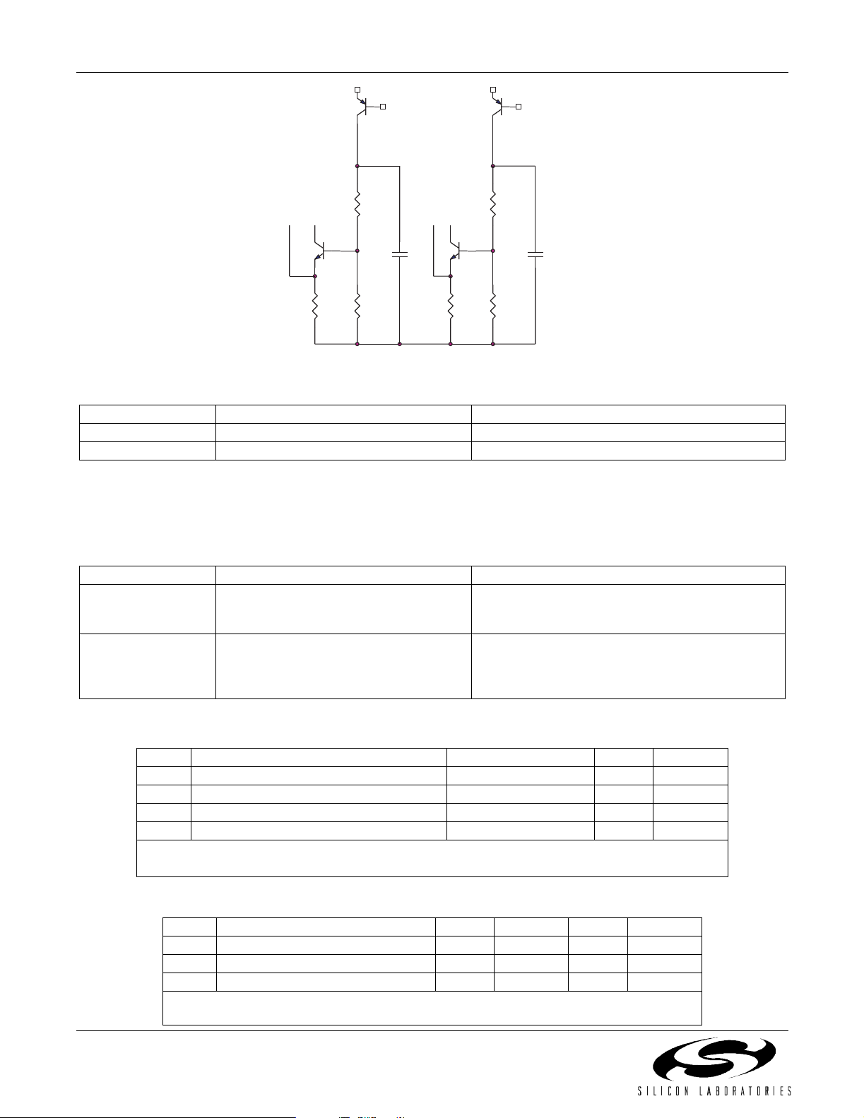
Figure 13. Si321x Optional Equivalent Q5, Q6 Bias Circuit
Table 16. Si321x Optional Bias Component Values
Component Value Supplier/Part Number
C7,C8 100 nF, 100 V, X7R, ±20% Murata, Johanson, Venkel
R23,R24 3.0 kΩ, 1/10 W, ±5%
The subcircuit above can be substituted into any of the ProSLIC solutions as an optional bias circuit for Q5, Q6. For
this optional subcircuit, C7 and C8 are different in voltage and capacitance to the standard circuit. R23 and R24 are
additional components.
Table 17. Component Value Selection for Si3210/Si3210M
Component Val ue Comments
R28 1/10 W, 1% resistor
For V
For V
= 3.3 V: 26.1 kΩ
DD
= 5.0 V: 37.4 kΩ
DD
R29 1/10 W, 1% resistor
For V
For V
For V
= 80 V: 541 kΩ
CLAMP
= 85 V: 574 kΩ
CLAMP
= 100 V: 676 kΩ
CLAMP
where V
where V
R28 = (V
BE
R29 = V
CLAMP
+ VBE)/148 µA
DD
is the nominal VBE for Q9
/148 µA
CLAMP
is the cl amping voltage for V
BAT
Tab le 18. Compo nent Value Selection Examples for Si3210M MOSFET/Transformer DC-DC Converter
VDC Ringing Load/Loop Resistance Transformer Ratio R18 R19, R20
3.3 V 3 REN/117 Ω 1 - 2 0.56 Ω 7.15 kΩ
5.0 V 5 REN/117 Ω 1 - 2 0.10 Ω 16.5 kΩ
12 V 5 REN/1 17 Ω 1 - 3 0.68 Ω 56.2 kΩ
24 V 5 REN/1 17 Ω 1 - 4 2.20 Ω 121 kΩ
Note: There ar e other system and software condit ions that influen ce component value selection, so pl ease refer to
AN45 “Design Guide for the Si3210 DC -DC Conv er ter for detailed guidance.
Table 19. Component Value Selection Examples for Si3210 BJT/Inductor DC-DC Converter
VDC Ringing Load/Loop Length L1 R17 R18 R19, R20
5 V 3 REN/11 7 Ω 33 µH100Ω 0.12Ω 16.5 kΩ
12 V 5 REN/117Ω 150 µH162Ω 0.56Ω 56.2kΩ
24 V 5 REN/117Ω 560 µH274Ω 2.2 Ω 121 kΩ
Note: There are other s ystem and software conditions that influence component value selection, so
please refer to AN45 “Design Guide for the Si3210 DC-DC Converter for detailed guidance.
20 Preliminary Rev. 1.11
Functional Description
t
Si3210/Si3211/Si3212
The ProSLIC™ is a single low-voltage CMOS device
that provides all the SLIC, codec, DTM F detection, and
signal generation functions needed for a complete
analog telephone interface. The ProSLIC performs all
battery, overvoltage, ringing, supervision, codec, hybrid,
and test (BORSCHT) function s. Unlike most monolithic
SLICs, the Si3210 does not require externally supplied
high-voltage battery supplies. Instead, it generates all
necessary battery voltages from a positive dc supply
using its own dc-dc converter controller. Two fully
programmable tone generators can produce DTMF
tones, phase continu ous FSK (caller ID) signaling, and
call progress tones. DTMF decoding and pulse metering
signal generation are also integrated.
The ProSLIC is ideal for short loop applications, such as
terminal adapters, cable telephony, PBX/key systems,
wireless local loop (WLL) , and voice over IP solutions.
The device meets all relevant LSSGR and CCITT
standards.
The linefeed provides programmable on-hook voltage,
programmable off-hook loop current, reverse battery
operation, loop or gro und start operation, and on-hook
transmission ringing voltage. Loop curr ent and voltage
are continuously monitored using an integrated A/D
converter. Balanced 5 REN ringing with or without a
programmable dc offset is integrated. The available
offset, frequency, w aveshape, and cadence options are
designed to ri ng the widest variety of terminal devices
and to reduce external controller re quirem ents.
A complete audio transmit and receive path is
integrated, including DTMF decoding, ac impedance,
and hybrid gain. These features are software
programmable, all owing for a single hardwar e design to
meet international requirements. Digital voice data
transfer occurs over a standard PCM bus. Cont rol data
is transferred using a standard SPI. The device is
available in a 38-pin TSSOP.
Linefeed Interface
The ProSLIC’s linefeed interface offers a rich set of
features and programmable flexibility to meet the
broadest applications requirements. The dc linefeed
characteristics are software program mable; key current,
voltage, and power measurements are acquired in
realtime and provided in software registers.
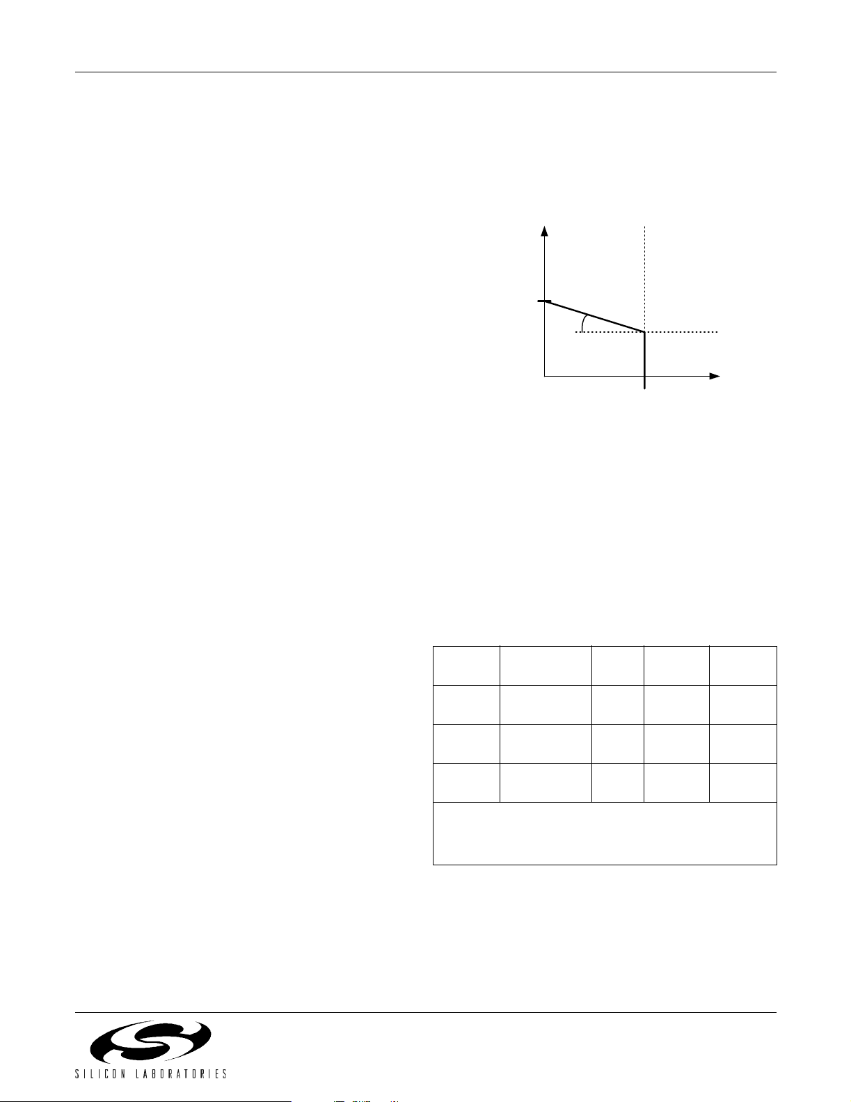
1.5 V steps. The loop current limit (I
) defines the
LIM
constant current zone and is programmable from 20 mA
to 41 mA i n 3 mA steps. The ProSLIC has an inherent
dc output resistance (R
V
(TIP-RING)
V
(V)
OC
) of 160 Ω.
O
Constant
Voltage
Zone
R
=160 Ω Constant Curren
O
I
LIM
Zone
I
LOOP
(mA )
Figure 14. Simplified DC Current/Voltage
Linefeed Characteristic
The TIP-to-R ING v oltage (VOC) is offset from ground by
a programmable voltage (V
) to provide voltage
CM
headroom to the posit ive-most terminal (TIP in forward
polarity states and RING in reverse polarity states) for
carrying audio signals. Table 20 summarizes the
parameters to be initialized before entering an active
state.
Table 20. Programmable Ranges of DC
Linefeed Character i stics
Parameter Programmable
I
LIM
V
OC
V
CM
*Note: The ProSLIC uses registers that are both directly
and indirectly mapped. A “direct” regist er is one that
is mapped directly.
Range
20 to 41 mA 20 mA ILIM[2:0] Direct
0 to 94.5 V 48 V VOC[5:0] Direct
0 to 94.5 V 3 V VCM[5:0] Direct
Default
Value
Register
Bits
Location*
Register 71
Register 72
Register 73
DC Feed Characteristics
The ProSLIC has pro grammable constant v oltage and
constant current zones as depicted in Fig ure 14. Open
circuit TIP-to-RING voltage (V
) defines the c onstant
OC
voltage zone and is programmable from 0 V to 94.5 V in
Preliminary Rev. 1.11 21

Si3210/Si3211/Si3212
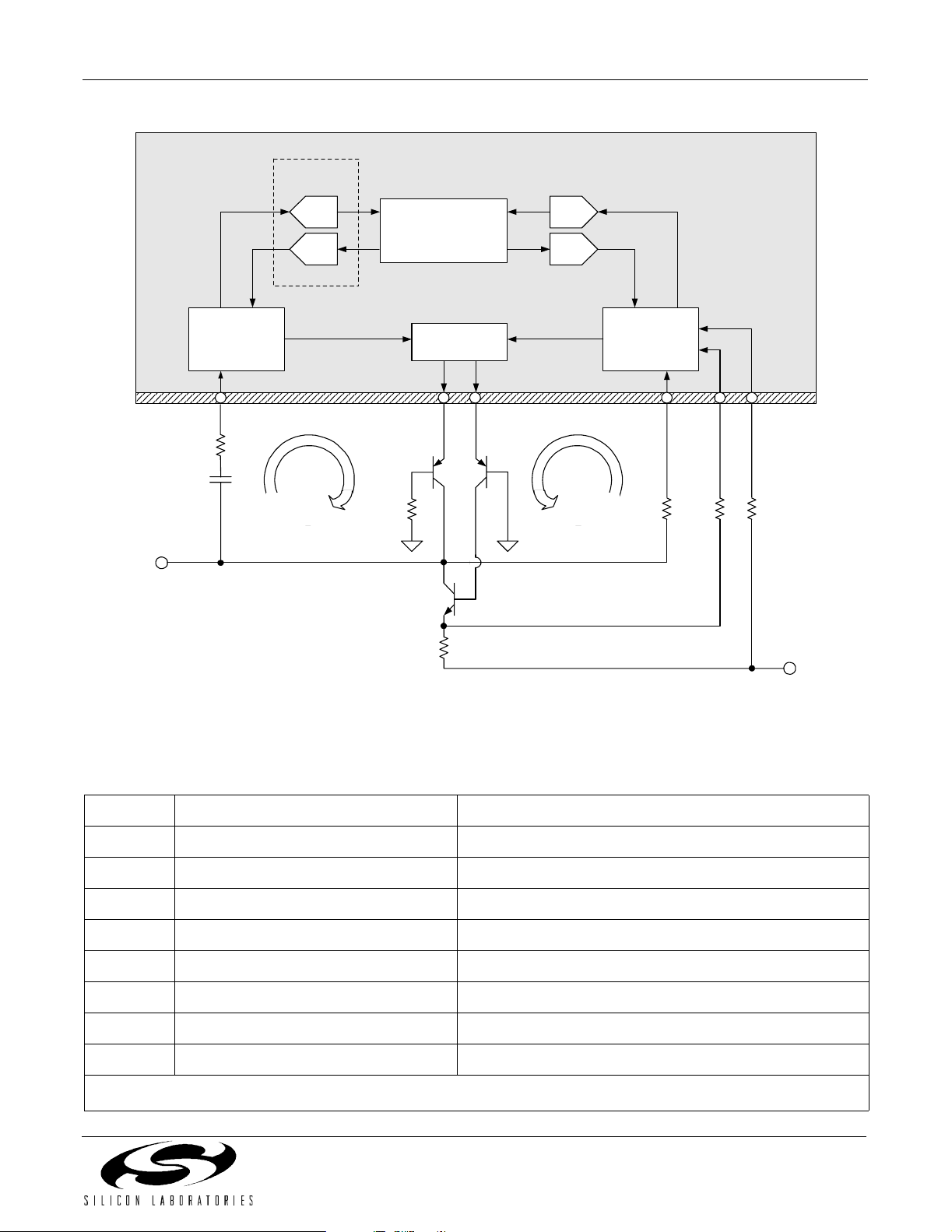
Linefeed Architecture
The ProSLIC is a low-voltage CMOS d evice that uses
low-cost external components to control the high
voltages required for subscriber line interfaces.
Figure 15 is a simplified illustration of the linefeed
control loop circuit for TIP or RING and the external
components used.
The ProSLIC uses both voltage and c urrent sensing to
control TIP and RING. DC and AC line voltage s on TIP
and RING are measured through sense resistors R
DC
and RAC, respectively. The ProSLIC uses linefeed
transistors Q
and QN to drive TIP and RING. Q
P
DN
isolates the high-voltage base of QN from the ProSLIC.
The ProSLIC measures voltage at various nodes in
order to monitor the linefeed current. R
provide access to these measuring points. The
R
BAT
, RSE, and
DC
sense circuitry is calibrated on-chip to guarantee
measurement accuracy with standard external
component tolerances. See "Linefeed Calibration" on
pa ge 26 for det ails.
Linefeed Operation States
The ProSLIC linefeed has eight states of operatio n as
shown in Table 21. The state of operation is controlled
using the Linefeed Control register ( direc t Regis ter 64).
The open state turns off all currents into the external
bipolar transistors and can be used in the presence of
fault conditions on the line and to generate Open Switch
Intervals (OSIs). TIP and RING a re effectivel y tri-stated
with a dc output impedance of about 150 k
Ω. The
ProSLIC can also automat ic ally ent er the open state if it
detects excessive power being consumed in the
external bipolar transist ors. See "Power Monitoring and
Line Fault Detection" on page 24 for more details.
In the forward active and reverse ac tive states, linef eed
circuitry is on and the audio s ignal paths are powered
down.
In the forward and revers e on-hoo k transmis sion s tates
audio signal paths are powered up to provide data
transmission during an on-hook loop condition.
The TIP Open state turns off all control cur rents to the
external bipolar devices connec ted to TIP and provides
an active linefeed on RING for ground start operation.
The RING Open state provides similar operation with
the RING drivers off and TIP active.
The ringing state drives programmable ringing
waveforms onto the line.
Loop Voltage and Current Monitoring
The ProSLIC continuo usly monitors the TIP and RING
voltages and external BJT currents. These values are
available in regis ters 78–89. Table 22 o n page 24 lis ts
the values that are measured and their associated
registers. An internal A/D converter samples the
measured voltages and currents from the analo g sense
circuitry and translates them into the digital domain. The
A/D updates the samples at an 800 Hz rate. Two
derived values are also reported—loop voltage and loop
current. The loop v olta ge, V
TIP–VRING
, is reported as a
1-bit sign, 6-bit magnitude format. For ground start
operation the reported value is t he RING voltage. The
loop current, (I
– IQ2 + IQ5 –IQ6)/2, is reported i n a 1-
Q1
bit sign, 6-bit magnit ude format. In RING op en and TIP
open states the loop cu rrent is report ed as (I
–IQ6).
(I
Q5
– IQ2) +
Q1
22 Preliminary Rev. 1.11
Aud i o
Codec
Si3210/Si3211/Si3212
Monitor A/D
TIP or
RING
A/D
A/D
DSP
D/AD/A
SLIC DAC
AC
Control
R
C
AC
AC
AC Sense
AC
Control
Loop
R
BP
On-ChipExternal Components
Σ
Q
Q
DN
P
Q
N
R
E
DC
Control
Loop
DC
Control
DC Sense
R
DC
Battery Sense
Emitter Sense
R
SE
R
BAT
V
BAT
Figure 15. Simplified ProSLIC Linefeed Architecture for TIP and RING Leads (One Shown)
Table 21. ProSLIC Linefeed Operations
LF[2:0]* Linefeed State Description
000 Open TIP and RING tri-stated.
001 For ward Active V
010 Forward On-Hook Transmission V
011 TIP Open TIP tri-state d, RING active; used for ground s tart.
100 Ringing Ringing waveform applied to TIP and RING.
101 Reverse Active V
110 Reverse On-Hook Transmission V
1 11 Ring Open RING tri-stated, TIP active.
Note: The Linefeed register (LF) is locat ed in direct Register 64.
TIP
TIP
RING
RING
> V
> V
> V
> V
.
RING
; audio signal paths powered on.
RING
.
TIP
; audio signal paths powered on.
TIP
Preliminary Rev. 1.11 23

Si3210/Si3211/Si3212
4096
P
h
Table 22. Measure d Re al ti me Linefe ed Interfa ce Charac ter i stics
Parameter Measurement
Loop Voltage Sense (V
TIP
– V
Range
) –94.5 to +94.5 V 1.5 V L V SP,
RING
Resolution Register
Bits
Location*
Direct Register 78
LVS[6:0]
Loop Current Sense –80 to +80 mA 1.27 mA LCSP,
Direct Register 79
LCS[5:0]
TIP Voltage Sense 0 to –95.88 V 0.376 V VTIP[7:0] Direct Register 80
RING Voltage Sense 0 to –95.88 V 0.376 V VRING[7:0] Direct Register 81
Battery Voltage Sense 1 (V
Battery Voltage Sense 2 (V
) 0 to –95.88 V 0.376 V VBATS1[7:0] Direct Register 82
BAT
) 0 to –95.88 V 0.376 V VBATS2[7:0] Direct Register 83
BAT
Transistor 1 Current Sense 0 to 81.35 mA 0. 319 m A IQ1[7: 0] Direct Register 84
Transistor 2 Current Sense 0 to 81.35 mA 0. 319 m A IQ2[7: 0] Direct Register 85
Transistor 3 Current Sense 0 to 9.59 mA 37.6
Transistor 4 Current Sense 0 to 9.59 mA 37.6
µA IQ3[7:0] Di r ect Regist er 86
µA IQ4[7:0] Di r ect Regist er 87
Transistor 5 Current Sense 0 to 80.58 mA 0. 316 m A IQ5[7: 0] Direct Register 88
Transistor 6 Current Sense 0 to 80.58 mA 0. 316 m A IQ6[7: 0] Direct Register 89
*Note: The ProSLIC uses registers that are both directly and i ndi rectly mapped. A “direct” regi ster is one that is mapped
directly.
Power Monitoring and Li ne Fa u lt D et ec ti on
In addition to reporting voltages and currents, the
ProSLIC continuously monit ors the power dissipated in
the type of fault condition present on the line .
The value of each thermal low-pass filter pole is set
according to the equation:
each external bipolar t ransistor. Realtime output power
of any one of the six linefeed transistors c an be read by
setting the Power Monitor Pointe r (direct Regis ter 76) to
point to the des ir ed t r ansis tor and then reading the Line
Power Output Monitor (direct Register 77).
The realtime power measurem ents are low- pass filter ed
and compared to a maximum power threshold.
Maximum power thresholds and filter time constants are
software programmable and should be set for each
transistor pair based on the characteristics of the
transistors used. Table 23 describes the registers
associated with this function. If the power in any
---------------- -
800 τ⋅
where
thermal LPF register
τ is the thermal time constant of the transistor
package, 4096 is the full range of the 12-bit register, and
800 is the sample rate in hertz. Ge ner ally
for SOT223 packages and
τ = 0.16 seconds f or SO T23,
but check with the manufacturer for the package
thermal con stant of a specif ic device. F or example, t he
power alarm threshol d and low-pass filt er values fo r Q5
and Q6 using a SOT223 package transistor are
computed as follows:
3
2
⋅=
τ = 3 seconds
external transisto r exceeds the programm ed threshold,
a power alarm event is tri ggered. The ProSLIC sets the
Power Alarm register bit, generates an interrupt (if
enabled), and automatically enters the Open state (if
AOPN = 1). This feature protects the external
transistors from fault con ditions and , com bined wit h the
loop voltage and current m onitors, allows diagnosis of
MAX
PPT56
-------------------------------
====
Resolution
Thus, indirect Register 34 should be set to 150Dh.
Note: The power monitor resolution for Q3 and Q4 is differen t
from that of Q1, Q2, Q5, and Q6.
7
1.28
------------------
2
⋅
0.0304
7
2
⋅ 5389 150D
24 Preliminary Rev. 1.11

Si3210/Si3211/Si3212
Table 23. Associated Power Monitoring and Power Fault Registers
Parameter Description/
Range
Power Monit o r Po i nter 0 to 5 points to Q 1
to Q6, respe ctively
Line Power Monitor Output 0 to 7.8 W for Q1,
Q2, Q5, Q6
0 to 0.9 W for Q3,
Q4
Power Alarm Threshold, Q1 & Q2 0 to 7.8 W 30.4 mW PPT12[7:0] Indirect Register 32
Power Alarm Threshold, Q3 & Q4 0 to 0.9 W 3.62 mW PPT34[7:0] Indirect Register 33
Power Alarm Threshold, Q5 & Q6 0 to 7.8 W 30.4 mW PPT56[7:0] Indirect Register 34
Thermal LPF Pole, Q1 & Q2 see equation above NQ12[7:0] Indirect Register 37
Thermal LPF Pole, Q3 & Q4 see equation above NQ34[7:0] Indirect Register 38
Thermal LPF Pole, Q5 & Q6 see equation above NQ56[7:0] Indirect Register 39
Power Alarm Interrupt Pending Bits 2 to 7 corre-
spond to Q1 to Q6,
respectively
Resolution Register
Bits
n/a PW RM P[2: 0] Direct Register 76
30.4 mW
3.62 mW
n/a QnAP[n+1],
PWROM[7:0] Direct Regis t er 77
where n =1
to 6
Location*
Direct Register 19
Power Alarm Interrupt Enable Bits 2 to 7 corre-
spond to Q1 to Q6,
respectively
Power Alarm
Automatic/Manual Detect
*Note: The ProSLIC uses registers that are both directly and i ndi rectly mapped. A “direct” regi ster is one that is mapped
directly. An “indirect” register i s one that is accessed using the indirect access regist ers (direct registe rs 28 th rough
31).
0 = manual mode
1 = enter open state
upon power alarm
n/a QnAE[n+1],
where n = 1
to 6
n/a A OP N Direct Register 67
Direct Register 22
Preliminary Rev. 1.11 25
Si3210/Si3211/Si3212
LCS
LVS
Input
Signal
Processor
LCVELFS
ISP_ OU T
Digital
LPF
NCLR
HYSTEN
Loop Closure
Threshold
LCRTLLCRT
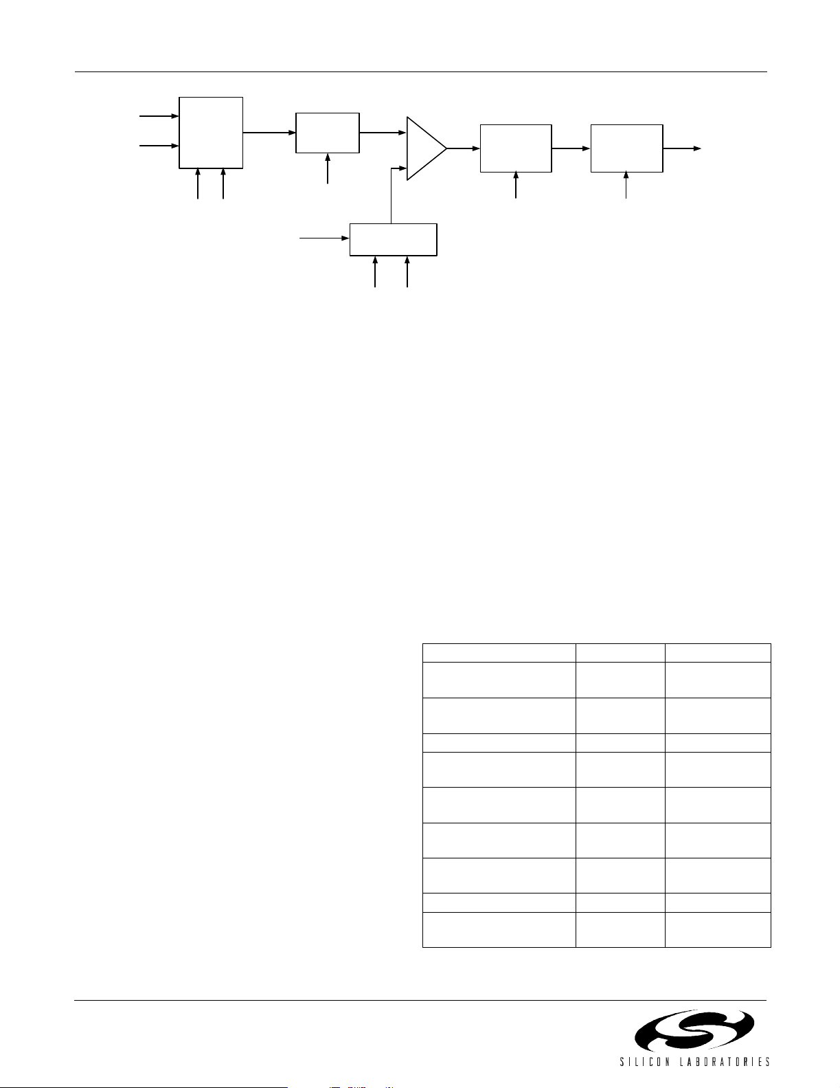
Figure 16. Loop Closure Detection
Loop Closure Detection
A loop closure event signals that the terminal equipment
has gone off-hook durin g on-hook transmission or onhook active states. The ProSLIC perform s loop closure
detection digitally using its on-chip monitor A/D
converter. The functional bloc ks required to implement
loop closure detection are shown in Figure 16. The
primary input to the system is the Loop Current S ense
value provided in the LCS register (direct Register 79).
The LCS value is processed in the Input Signal
Processor when the ProSLIC is in the on-hook
transmission or on-hook active linefeed state, as
indicated by the Linefeed Shadow register, LFS[2:0]
(direct Register 64). The data then feeds into a
programmable digital low-pass filter, which removes
unwanted ac signal components before threshold
detection.
The output of the low-pass filter is compared to a
programmable threshold, LCRT (indirect register 28).
The threshold comparator output feeds a programmable
debouncing filter. The output of the debouncing filter
remains in its pres ent state unles s the input remains in
the opposite state for the entire period of time
programmed by the loop closure debounce interval,
LCDI (direct Regist er 69). I f the debounce interval has
been satisfied, th e LCR bit will be se t to indicate that a
valid loop closure has oc c urr ed. A loop closure interru pt
is generated if enabled by the LCIE bit (direct
Register 22). Table 24 lists the registers that must be
written or monitored to correctly detect a loop closure
condition.
Loop Closu r e Threshold H y st ere sis
Silicon revisions C and higher support the addition of
programmable hyste resis to the loop closu re threshold,
which can be enabled by setting HYSTEN = 1 (direct
Register 108, b it 0). The hyst eresis is defined b y LCRT
(indirect Register 28) and LCRTL (indirect Regi ster 43),
+
Debo un ce
Filter
–
LCDI
LCR
Interrupt
Logic
LCIE
LCIP
which set the upper and lower bounds, res pec tive ly.
Voltage-Based Loop Closure Detection
Silicon revisions C and highe r also support an optional
voltage-based loop closure detection mode, which is
enabled by setting LCVE = 1 (direct Register 108,
bit 2). In this mode t he loop voltage is co mpared to the
loop closure threshold register (LCRT) which represents
a minimum voltage threshold instead of a maximum
current threshold. If hysteresis is also enabled, then
LCRT represents the upper voltage boundary and
LCRTL represents the lower voltage boundary for
hysteresis. Although voltage-based loop closure
detection is an option, the default current-based loop
closure detection is recommended.
Table 24. Register Set for Loop
Closure Detection
Parameter R egi ster Location
Loop Closure
Interrupt Pending
Loop Closure
Interrupt Enable
Loop Closure Threshold LCRT[5:0] Indir ect Reg. 28
Loop Closure
Threshold—Lower
Loop Closure Filter
Coefficient
Loop Closure Detect
Status (monitor only)
Loop Closure Detect
Debounce Interval
Hysteresis Enable HYSTEN Direct Reg. 108
Voltage-Based Loop
Closure
Linefeed Calibra t i on
LCIP Direct Reg. 19
LCIE Direct Reg. 22
LCRTL[5:0] Indirect Reg. 43
NCLR[12:0] Indirect Reg. 35
LCR Direct Reg. 68
LCDI[6:0] Direct Reg. 69
LCVE Direct Reg. 108
26 Preliminary Rev. 1.11

Si3210/Si3211/Si3212
An internal calibration algorithm corrects for internal and
external component errors. The calibration is initiated by
setting the CAL bit in direct Register 96. Upon
completion of the calibration cycle, this bit is
automatically reset.
It is recommended that a calibration be executed
following system power-up. Upon release of the chip
reset, the Si3210 will be in the open state. After
powering up the dc-dc converter and allowing it to settle
for time (t
) the calibration can be initiated.
settle
Additional calibrations may be performed, but only one
calibration should be necessary as long as t he system
remains powered up.
During calibration, V
BAT
, and V
TIP
voltages are
RING
, V
controlled by the calibration engine to provide the
correct external voltage conditions for the algorithm.
Calibration should be performed in the on-hook state.
RING or TIP must not be connected to ground during
the calibration.
Battery Voltage Generation and Switching
The ProSLIC supports two modes of battery supply
operation. First, the Si3210 integrates a dc-dc converter
controller that dynamically regulates a single output
voltage. This mode eliminates t he need to suppl y large
external battery voltages. Instead, it converts a single
positive input voltage into the real-t ime battery voltage
needed for any given state according to programmed
linefeed parameters. Second, the Si3211 and Si3212
support switching between high and low battery voltage
supplies, as would a traditional monolithic SLIC.
For single to low channel count applications, the Si3210
proves to be an economical choice, as the dc-dc
converter eliminate s the need to design and build highvoltage power supplies. For higher channel count
applications whe re cent ralized batt ery voltag e supp ly is
economical, or for modular legacy systems where
battery voltage is already available, the Si3211 and
Si3212 are recommended.
DC-DC Converter General Description
(Si3210/Si3210M Only)
The dc-dc converter dynamically generates the large
negative voltages required to operate the linefeed
interface. The Si3210 ac ts as the controller for a buckboost dc-dc converter that converts a positive dc
voltage into the desired negative battery voltage. In
addition to eliminating external power supplies, this
allows the Si3210 to dynamically control the battery
voltage to the minimum r equired for any given mode of
operation.
Two different dc-dc circuit options are offered: a BJT/
inductor version and a MOSFET/transformer version.
Due to the differences on the drivi ng circuits, there are
two different versions of the Si3210. The Si3210
supports the BJT/inductor circuit option, and the
Si3210M version supports the MOSFET solution. The
only difference bet ween the two versions is the polarity
of the DCFF pin with respect to the DCDRV pin. For the
Si3210, DCDRV and DCFF are opposite polarity. For
the Si3210M, DCDRV and DCFF are the sam e polarity.
Table 25 summarizes these differences.
Table 25. Si3210 and Si3210M Differences
Device DCFF Signal
Polarity
Si3210
= DCDRV
Si3210M = DCDRV 1
Notes:
1.
DCFF signal polarity wit h respect to DCDRV signal.
2. Di rect Register 93, bit 5; This is a read-only bit.
Extensive design guidance on each of these circuits can
be obtained from Application Note 45 (AN45) and from
an interactive dc-dc converter design spreadsheet. Both
of these documents are available on the Silicon
Laboratories website (www.silabs.com).
BJT/Inductor Circuit Option Using Si3210
The BJT/Inductor circuit option, as defined in Figure 9,
offers a flexible, low-cost solution. Depending on
selected L1 inductance value and the switching
frequency, the input voltage (V
) can range from 5 V to
DC
30 V. By nature of a dc-dc converter ’s operation, peak
and average input currents can become large with small
input voltages. Consider this when selecting the
appropriate i nput voltage and pow er rating for the V
power supply.
For this solution, a PNP power BJT (Q7) switch es the
current flow through low E SR inductor L1. The Si3210
uses the DCD RV and DCFF pins to switch Q7 o n and
off. DCDRV controls Q7 t hrough NPN BJT Q8. DCFF is
ac coupled to Q7 through capacitor C10 to assist R16 in
turning off Q7. Therefore, DCFF must have opposite
polarity to DCDRV, and the Si321 0 (not Si321 0M) must
be used.
MOSFET/Transformer Circuit Option Using Si3210M
The MOSFET/transformer circuit option, as defined in
Figure 11, offers higher power efficiencies across a
larger input voltage range. Depending on the
transformers primary inductor value and the switching
frequency, the input voltage (V
) can range from 3.3 V
DC
to 35 V. Therefore, it is possible to power the entire
ProSLIC solution from a single 3.3 V or 5 V power
supply. By nature of a dc-dc converter’s operation, peak
DCPOL
0
DC
Preliminary Rev. 1.11 27

Si3210/Si3211/Si3212
and average input currents can become large with small
input voltages. Consider this when selecting the
appropriate input voltage and power rating for the V
DC
power supply (number of REN supported).
For this solution, an n-channel power MOSFET (M1)
switches the cur rent flow through a p ower transformer
T1. T1 is specified in Applicat ion Note 45 (AN45), and
includes several taps on the prim ary side to facilitate a
wide range of input voltages. The Si3210M version of
the Si3210 must be used for the application circuit
depicted in Figure 9 because the DCFF pin is used to
drive M1 directly and therefore must be the same
polarity as DCDRV. DCDRV is not used in this circuit
option; connecting DCFF and DCDRV together is not
recommended.
DC-DC Converter Architecture
(Si3210/Si3210M Only)
The control logic for a pulse width modulated (PWM) dcdc converter is incor porated in the S i3210. O utput pins ,
DCDRV and DCFF, are used to switch a bipolar
transistor or MOSFET. The polarity of DCFF is opposite
to that of DCDRV.
The dc-dc converter circuit is powered on when the
DCOF bit in the Power Down Register (direct
Register 14, bit 4) is cleared to 0.
The switching
regulator circuit within the Si3210 is a high
performance, pulse-width modulation controller. The
control pins are driven by the PWM controller logic in
the Si3210. The regulated output voltage (V
BA T
) is
sensed by the SVBAT pin and is used to detect whether
the output voltage is above or below an internal
reference for the desired battery voltage. The dc
monitor pins SDCH and SDCL monitor input current and
voltage to the dc-dc converter external circuitry. If an
overload condition is detected, the PWM controller w ill
turn off the sw itching transistor for the remainder of a
PWM period to prevent damage to external
components. It is important that the proper val ue of R18
be selected to ensure safe operation. Guidance is given
in Application Note 45 (AN45).
The PWM co ntroller o perates at a frequency se t by t he
dc-dc Converter PWM register (direct Register 92).
During a PWM period the outputs of the control pins
DCDRV and DCFF are asserted for a time given by the
read-only PWM Pulse Width register (direct
Register 94).
The dc-dc converter must be off for some time in each
cycle to allow the inductor or trans former to trans fer its
stored energy to the output capacitor, C9. This minimum
off time can be set through the dc-dc Converter
Switching Delay register, (direct Register 93). The
number of 16.384 MHz clock cycles that the controller is
off is equal to DCTOF (bits 0 throug h 4) plus 4. I f the dc
Monitor pins detect an overload condition, the dc-dc
converter interru pts its conversion cycles regardl ess of
the register settings to prevent component damage.
These inputs should be calibrated by writing the DCCAL
bit (bit 7) of the dc-dc Converter Switching Delay
register, direct Register 93, after the dc-dc converter
has been turned on.
Because the Si3210 dynamically regulates its own
battery supply voltage using the dc-dc converter
controller, the battery vo ltage (V
) is offset from the
BAT
negative-most terminal by a programmable voltage
) to allow voltage headroom for carrying audio
(V
OV
signals.
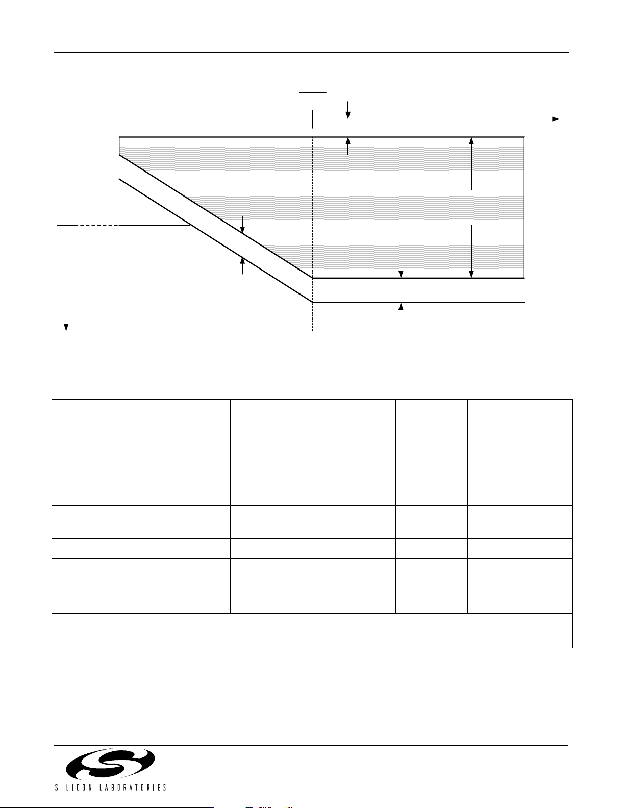
As mentioned previously, the Si3210 dynamically
adjusts V
illus tra te th i s, the be h av ior of V
to suit the particular circuit requirement. To
BAT
in the active state is
BAT
shown in Figure 17. In the active state, the TIP-t o- RING
open circuit voltage is kept at V
voltage region while the regulator output voltage, V
+ VOC + VOV.
V
CM
When the loop cu rrent attempts to exceed I
in the constant
OC
, the dc
LIM
BAT
=
line driver c ircuit ent ers cons tant current mode a llowing
the TIP to RING voltage to track R
. As the TIP
LOOP
terminal is kept at a constant voltage, it is the RING
terminal voltag e that tracks R
| voltage will als o track R
|V
BAT
R
= I
LIM
the VOC/I
continue to track R
+ VCM +VOV. As R
LOOP
mark, the regulator output voltage can
LIM
(TRACK = 1), or the R
LOOP
tracking mechanism is stopped when |V
and, as a result, the
LOOP
. In this state, |V
LOOP
decreases below
LOOP
BAT
| = |V
BAT
LOOP
BATL
(TRACK = 0). The former case is the more common
application and provides the maximum power
dissipation savings. In principle, the regulator output
voltage can go as low as |V
|=VCM+ VOV, offeri ng
BAT
significant powe r savings.
When TRACK = 0, |V
. The RING t erminal voltage, howev er, continues
V
BATL
to decrease with decreasing R
| will not decrease below
BAT
. The power
LOOP
dissipation on the NPN bipolar transistor driving the
RING terminal can become large and may require a
higher power rat ing device. The non-trac king mode of
operation is required by specific terminal equipment
which, in order to initiate certain data transmission
modes, goes briefly on-hook to measure the line voltage
to determine whether there is any other off-hook
terminal equipmen t on the same line. TRACK = 0 mode
is desired since the regulator output voltage has long
settling time constants (on the order of tens of
milliseconds) and cannot change ra pidly for TRACK = 1
mode. Therefore, the brief on-hook voltage
measurement would yield approximately the same
voltage as the off-hook line voltage and would cause the
terminal equipment to incorrectly sense another offhook terminal.
|
|
28 Preliminary Rev. 1.11
V
V
V
BATL
T
R
A
C
TRACK=0
Si3210/Si3211/Si3212
OC
I
Constant I Re gi on Consta nt V Region
K
=
1
V
OV
LIM
|V
TIP
V
CM
- V
RING
|
V
OV
R
LOOP
V
TIP
V
OC
V
RING
V
BAT
Figure 17. V
TIP
, V
RING
, and V
in the For ward Acti ve State
BAT
Table 26. Associated Relevant DC-DC Converter Registers
Parameter Range Resolution Register Bit Location
DC-DC Converter Power-off
Control
DC-DC Converter Calibration
Enable/Status
DC-DC Converter PWM Period 0 to 15.564 us 61.035 ns DCN[7:0] Direct Register 92
DC-DC Converter Min. Off Time (0 to 1.892 us ) +
High Battery Voltage—V
Low Battery Voltage—V
V
OV
Note: The ProSLIC uses registers that are both directly and i ndi rectly mapped. A “direct” regi ster is one that is mapped
directly. An “indirect” register is one that i s accessed using the indirect access registers (direct r egisters 28 thr ough 31).
BATH
BATL
n/a n/a DCOF Direct Regist er 14
n/a n/a DCCAL Direct Register 93
61.035 ns DCTOF[4:0] Direct Register 93
4ns
0 to –94.5 V 1.5 V VBATH[5:0] Direct Reg i s ter 74
0 to –94.5 V 1.5 V VBATL[5:0] Direct Regist er 75
0 to –9 V or
0 to –13.5 V
1.5 V VMIND[ 3:0 ]
VOV
Indirect Register 41
Direct Register 66
Preliminary Rev. 1.11 29

Si3210/Si3211/Si3212
DC-DC Converter Enhancements
Silicon revisions C and higher support two
enhancements to the dc-dc converter. The first is a
multi-threshold er ror control algorithm tha t enables the
dc-dc converter to adjust more quickly to voltage
changes. This option is enabled by setting DCSU = 1
(direct Register 108, bit 5). The se cond enhancement is
an audio band filter that removes audio band noise from
the dc-dc co nverter contro l loop. This o ption i s ena bled
by setting DCFIL = 1 (direct Register 108, bit 1).
DC-DC Converter During Ringing
When the ProSLIC enters the ringing state, it requires
voltages well above those used in the acti ve mo de. The
voltage to be generated and regulated by the dc-dc
converter during a ringin g burst is set us ing the VBATH
register (direct Register 74). VBATH can be set between
0 and –94.5 V in 1.5 V steps. To avoid clipping the
ringing signal, V
amplitude. At the end of each ringing burst the dc-dc
converter adjusts back to active state regulation as
described above.
External Battery Switching (Si3211 and Si3212 Only)
The Si3211 and Si3212 support switching between two
battery voltages. The circuit for external battery
switching is defined in Figure 12. Typically a high
voltage battery (e.g., –70 V) is used for on-hook and
ringing states, and a low v oltage battery (e.g., –24 V) is
used for the off-hook condition. The ProSLIC uses an
external transistor to switch bet ween th e two s upplies.
When the ProSLIC changes operating states, it
automatically sw it c hes bat t er y s upplies if the au tom at ic /
manual control bit ABAT (direct Register 67, bit 3) is set.
For example, the ProSLI C will switch from high batte ry
to low battery when it detects an off-hook ev ent t hr ough
either a ring trip or loop closure event. If automatic
battery selection is disabled (ABAT = 0), the battery is
selected by the Batt ery Feed Select bit, BATSL (direct
Register 66, bit 1).
Silicon revisions C and higher support the option to add
a 60 ms debounce period to the battery switching circuit
when transitioning from high batt ery to low batte ry. This
option is enabled by setting SWDB = 1 (direct
Register 108, bit 3). This debounce minimizes battery
transitions in the case of pulse dialing or other quick onhook to off-hook transitions.
must be set larger than the ringing
BATH
Tone Generation
Two digital tone generators are provided in the ProSLIC.
They allow the gener ation of a wide variety of single or
dual tone frequency and amplitude combinations and
spare the user the effort of generating the required
POTS signaling tones on the PCM highway. DTMF, FSK
(caller ID), call progress, and other tones can all be
generated on -chip. The tones can be sent t o either t he
receive or transmit paths (see Figure 23 on page 40).
Tone Generator Architecture
A simplified dia gram of the tone gener ator architecture
is shown in Figure 18. The oscillator, active/inactive
timers, interrupt block, and signal routing block are
connected to give the user flexibility in creating audio
signals. Control and status register bits are placed in the
figure to indicate their association with the tone
generator architect ur e. These r egisters are described in
more detail in Table 27.
30 Preliminary Rev. 1.11
 Loading...