Si3000
R
V
OICEBAND
C
ODEC WITH
M
ICROPHONE
Features
Complete voice codec solution includes the following:
!
84 dB ADC Dynamic Range
!
84 dB DAC Dynamic Range
!
4–12 kHz Sample Rates
!
30 dB Microphone Pre-Amp
!
Programmable Input Gain/
Attenuation: –36 dB to 12 dB
!
Programmable Output Gain/
!
Support for 32 Ω Headphones
!
3:1 Analog Input Mixer
!
3.3–5.0 V Power Supply
!
Direct Interface to DSPs
!
Direct Connection to Si3034,
Si3035, and Si3044 ISOcap
!
Low profile 16 Pin SOIC Package
™
DAA
Attenuation: –36 dB to 12 dB
Applications
!
Modem Voice Channel (DSVD)
!
Telephony
!
Speech Processing
!
General Purpose Analog I/O
Description
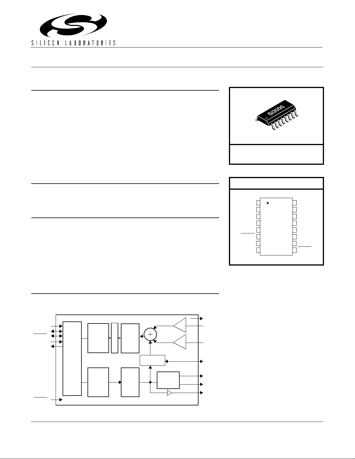
The Si3000 is a complete voice band audio codec solution that offers high
integration by incorporating programmable input and output gain/
attenuation, a microphone bias circuit, handset hybrid circuit, and an
output drive for 32 Ω headphones. The Si3000 c an be connec ted di rectly
to the Si3034, Si3035, and Si3044 ISOcap North American and
international DAA chipsets through its daisy-chaining serial interface. The
device operates from a singl e 3.3 to 5 V power supply and is avail able in
a 16-pin small outline package (SOIC).
/S
PEAKER
Ordering Information:
See page 30.
Pin Assignments
Si3000
SPKRR
MBIAS
HDST
FSYNC
MCLK
SCLK
SDI
SDO
1
2
3
4
5
6
7
8
D
16
15
14
13
12
11
10
9
RIVE
SPKRL
LINEO
GND
V
A
V
D
LINEI
MIC
RESET
Functional Block Diagram
Si3000
0/+10/+20/+30 dB
MCLK
SCLK
FSYNC
SDI
SDO
RESET
Digital
Interface
Prog Gain/
Attenuator
Prog Gain/
Attenuator
High Pass Filter
ADC
0/+10/+20 dB
Handset
Hybrid
0/–6/–12/–18 dB
Headphone
DriverDAC
0/–6/–12/–18 dB
Rev. 1.1 6/00 Copyright © 2000 by Silicon Laboratories Si3000-DS11
MBIAS
MIC
LINEI
HDST
SPKR
SPKRL
LINEO

Si3000
2 Rev. 1.1

Si3000
T
ABLE OF
C
ONTENTS
Section Page
Electrical Specifications . . . . . . . . . . . . . . . . . . . . . . . . . . . . . . . . . . . . . . . . . . . . . . . . . 4
Functional Description . . . . . . . . . . . . . . . . . . . . . . . . . . . . . . . . . . . . . . . . . . . . . . . . . . 14
Analog Inputs . . . . . . . . . . . . . . . . . . . . . . . . . . . . . . . . . . . . . . . . . . . . . . . . . . . . . . . 14
Pre-amp/Microphone Bias Circuit . . . . . . . . . . . . . . . . . . . . . . . . . . . . . . . . . . . . . . . 14
Programmable Input Gain/Attenuation . . . . . . . . . . . . . . . . . . . . . . . . . . . . . . . . . . . . 14
Analog Outputs . . . . . . . . . . . . . . . . . . . . . . . . . . . . . . . . . . . . . . . . . . . . . . . . . . . . . 14
Programmable Output Gain/Attenuation . . . . . . . . . . . . . . . . . . . . . . . . . . . . . . . . . . 15
Line Output . . . . . . . . . . . . . . . . . . . . . . . . . . . . . . . . . . . . . . . . . . . . . . . . . . . . . . . . . 15
Speaker Output . . . . . . . . . . . . . . . . . . . . . . . . . . . . . . . . . . . . . . . . . . . . . . . . . . . . . 15
Digital Interface . . . . . . . . . . . . . . . . . . . . . . . . . . . . . . . . . . . . . . . . . . . . . . . . . . . . . 15
Clock Generation Subsystem . . . . . . . . . . . . . . . . . . . . . . . . . . . . . . . . . . . . . . . . . . . 17
Sleep Mode . . . . . . . . . . . . . . . . . . . . . . . . . . . . . . . . . . . . . . . . . . . . . . . . . . . . . . . . 18
Loopback Operation . . . . . . . . . . . . . . . . . . . . . . . . . . . . . . . . . . . . . . . . . . . . . . . . . . 19
Reducing Power-on Pop Noise . . . . . . . . . . . . . . . . . . . . . . . . . . . . . . . . . . . . . . . . . 19
Control Registers . . . . . . . . . . . . . . . . . . . . . . . . . . . . . . . . . . . . . . . . . . . . . . . . . . . . . . . 20
Ordering Guide . . . . . . . . . . . . . . . . . . . . . . . . . . . . . . . . . . . . . . . . . . . . . . . . . . . . . . . . . 30
Package Outline . . . . . . . . . . . . . . . . . . . . . . . . . . . . . . . . . . . . . . . . . . . . . . . . . . . . . . . . 31
Contact Information . . . . . . . . . . . . . . . . . . . . . . . . . . . . . . . . . . . . . . . . . . . . . . . . . . . . . 36
Rev. 1.1 3
Si3000
Electrical Specifications
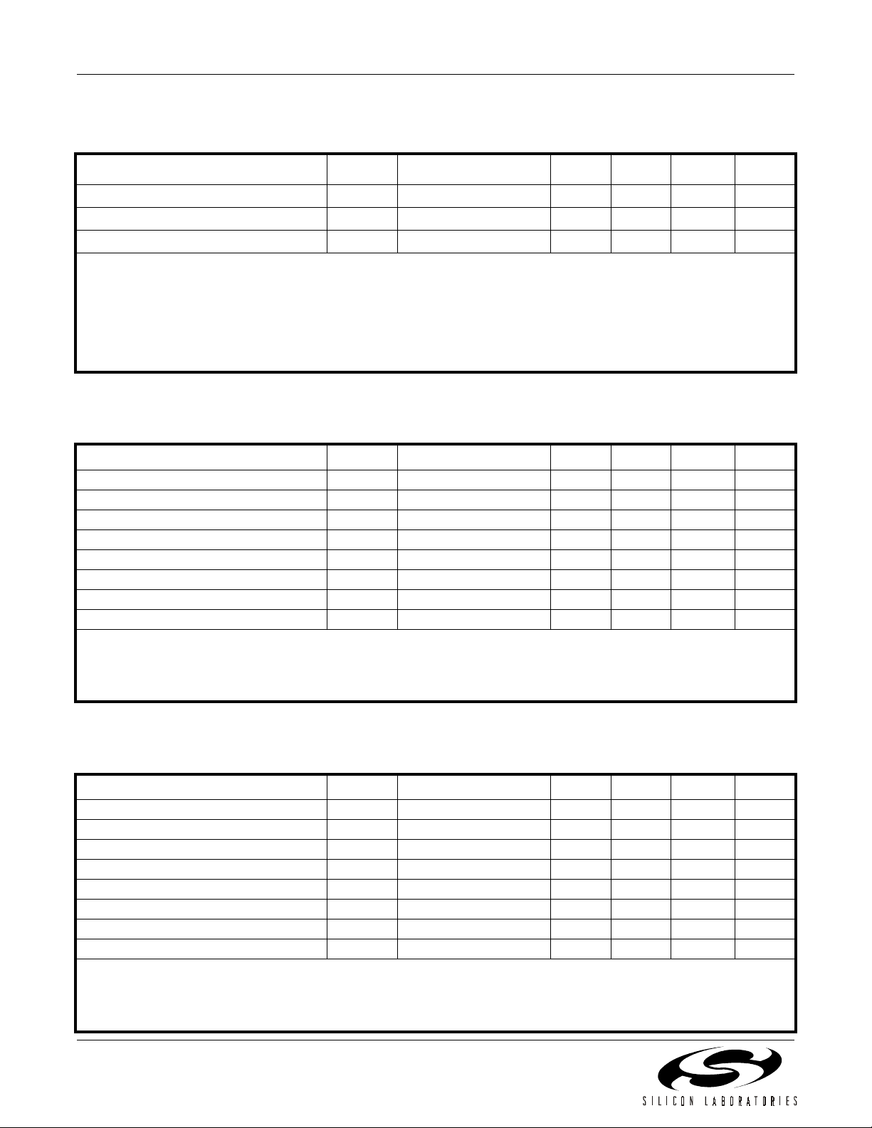
Table 1. Recommended Operating Conditions
Parameter Symbol Test Condition
Ambient Temperature T
Si3000 Supply Voltage, Analog
Si3000 Supply Voltage, Digital
2
2,3
A
V
A
V
D
K-grade 0 25 70 °C
1
Min
Typ
3.0 3.3/5.0 5.25 V
3.0 3.3/5.0 5.25 V
Max
1
Unit
Notes:
1. All minimum and maximum specifications are guaranteed and apply across the recommended operating conditions.
Typical values apply at nominal supply voltages and an operating temperature of 25°C unless otherwise stated.
2. The digital supply, V
3.3 V logic when operating from 3.3 V. V
3.
The Si3000 specifications are guaranteed using the typical application circuit (including component tolerance) of
and analog supply, VA, can operate from either 3.3 V or 5.0 V. The Si3000 supports interface to
D,
must be within 0.6 V of VA.
D
Figure 13.
Table 2. DC Characteristics, VA/VD = 5 V
(VA = 5 V ±5%, VD = 5 V ±5%, TA = 0 to 70°C for K-grade)
Parameter Symbol Test Condition Min Typ Max Unit
High Level Input Voltage V
Low Level Input Voltage V
High Level Output Voltage V
Low Level Output Voltage V
Input Leakage Current I
Power Supply Current, Analog
Power Supply Current, Digital
Total Supply Current, Sleep Mode
1
2
3
I
I
IH
IL
OH
OL
L
A
D
IO = –2 mA 3.5 — — V
IO = 2 mA — — 0.4 V
VA pin — 6.5 10 mA
VD pin — 10 15 mA
Notes:
1. No loads at D AC outputs, no load at MBIAS, Fs=12.5 kHz.
2.
Slave mode operation, Fs = 12.5 kHz.
3. All inputs, except MCLK, are held static, and all outputs are unloaded.
3.5 — — V
——0.8V
–10 — 10 µA
——1.5mA
Table 3. DC Characteristics, VA/VD = 3.3 V
(VA = 3.3 V ±10%, VD = 3.3 V ±10%, TA = 0°C to 70°C for K-grade)
Parameter Symbol Test Condition Min Typ Max Unit
High Level Input Voltage V
Low Level Input Voltage V
High Level Output Voltage V
Low Level Output Voltage V
Input Leakage Current I
Power Supply Current, Analog I
Power Supply Current, Digital
Total Supply Current, Sleep Mode
2
3
I
IH
IL
OH
OL
L
A
D
IO = –2 mA 2.4 — — V
IO = 2 mA — — 0.35 V
VA pin — 6 10 mA
VD pin — 6 10 mA
Notes:
1. No loads at D AC outputs, no load at MBIAS, Fs=12.5 kHz.
2. Slave mode operation, Fs = 12.5 kHz.
3. All inputs, except MCLK, are held static, and all outputs are unloaded.
4 Rev. 1.1
2.4 — — V
——0.8V
–10 — 10 µA
——1.5mA
Si3000
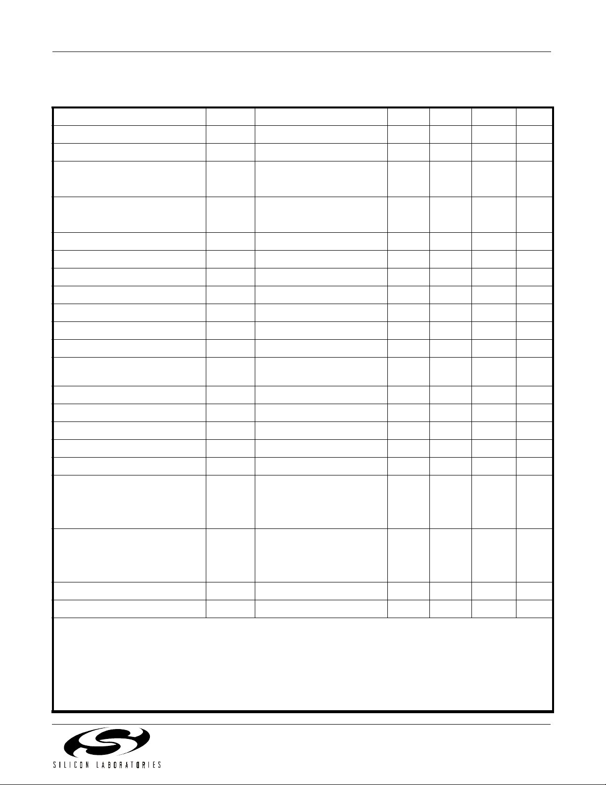
Table 4. AC Characteristics
(VA, VD = 5 V ±5% or 3.3 V ±10%, TA = 0°C to 70°C for K-grade)
Parameter Symbol Test Condition Min Typ Max Unit
ADC Resolution —16—Bits
ADC Dynamic Range
ADC Total Harmonic Distortion
1,2
3
VA, VD = 3.3 V ±10% VIN = 1 kHz, –3 dB, HDST — –80 –62
ADC Total Harmonic Distortion
3
VA, VD = 5 V ±5% VIN = 1 kHz, –3 dB, HDST — –80 –71
ADC Full Scale Level (0 dB gain)
ADC Programmable Input Gain –36 — 12 dB
ADC Input Gain Step Size — 1.5 — dB
ADC Freq Response
ADC Freq Response
5
5
ADC Freq Response F
Line In Preamp Gain — 0/10/20 — dB
ADCDR VIN = 1 kHz , –3 dB 80 84 — dB
ADCTHD VIN = 1 kHz, –3 dB, MIC/LINEI — –80 –62 dB
ADCTHD VIN = 1 kHz, –3 dB, MIC/LINEI — –80 –76 dB
4
V
RX
F
RR
F
RR
RR
Vin = 1 kHz — 1 — V
Low –3 dB corner — 33 — Hz
300 Hz –0.1 — 0 dB
3400 Hz –0.2 — 0 dB
rms
Mic In Preamp Gain — 0/10/20/
—dB
30
ADC Input Resistance 0 dB Preamp Gain — 20 — kΩ
ADC Input Capacitance — 15 — pF
ADC Gain Drift A
T
VIN = 1 kHz — 0.002 — dB/°C
DAC Resolution —16—Bits
DAC Dynamic Range
DAC Total Harmonic Distortion
VA, VD = 3.3 V ±10% VIN=1 kHz,–6 dB, SPKR, 60
DAC Total Harmonic Distortion
1,2
DACDR VIN = 1 kHz, –6 dB 80 84 — dB
3
3
DACTHD VIN=1 kHz,–6 dB,LINEO,600 Ω — –76 –60 dB
Ω
— –72 –60
VIN=1 kHz,–6 dB, HDST, 600
Ω
— –80 –70
DACTHD VIN=1 kHz,–3 dB,LINEO,600 Ω — –76 –65 dB
VA, VD = 5 V ±5% VIN=1 kHz,–3 dB, SPKR, 60 Ω — –72 –65
VIN=1 kHz,–3 dB, HDST, 600 Ω — –80 –76
DAC Full Scale Level (0 dB gain) V
RX
—1—V
rms
DAC Programmable Output Gain –36 — 12 dB
Notes:
1. DR = VIN + 20 log (RMS signal/RMS noise). Measurement bandwidth is 300 to 3400 Hz. Valid sample rate ranges
between 4000 and 12000 Hz.
2. 0 dB setting for analog and digital attenuation/gain.
3. THD = 20 log (RMS distortion/RMS signal). Valid sample rate ranges between 4000 and 12000 Hz.
4. At 0dB gain setting, 1 V
input corresponds to -1.5 dB of full scale digital output code.
rms
5. These characteristics are determined by external components. See Figure13.
6. With a 600 Ω load. Output starts clipping with half of full scale digital input, which corresponds to a 0.5 V
rms
output.
Rev. 1.1 5
Si3000
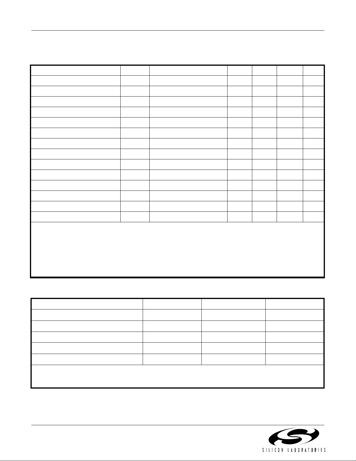
Table 4. AC Characteristics (Continued)
(VA, VD = 5 V ±5% or 3.3 V ±10%, TA = 0°C to 70°C for K-grade)
Parameter Symbol Test Condition Min Typ Max Unit
DAC Output Gain Step Size — 1.5 — dB
DAC Freq Response
DAC Freq Response
DAC Freq Response F
DAC Line Output Load Resistance 600 — — Ω
DAC Line Output Load Capacitance — — 40 pF
DAC SPKR Output Load Resistance — 60 — Ω
5
5
F
RR
F
RR
RR
Low –3 dB corner — 33 — Hz
300 Hz –0.01 — 0 dB
3400 Hz –0.2 — 0 dB
DAC Gain Drift A
T
VIN = 1 kHz — 0.002 — dB/°C
Interchannel Isolation (Crosstalk) — 90 — dB
HDST Full Scale Level Input — 0.5 — V
HDST Full Scale Level Output
6
—1.0—V
HDST Output Resistance Rout DC — 600 —
MIC Bias Voltage V
mbias
—2.5—V
MIC Power Supply Rejection Ratio PSRR — 40 — dB
Notes:
1.
DR = VIN + 20 log (RMS signal/RMS noise). Measurement bandwidth is 300 to 3400 Hz. Valid sample rate ranges
between 4000 and 12000 Hz.
2.
0 dB setting for analog and digital attenuation/gain.
3. THD = 20 log (RMS distortion/RMS signal). Valid sample rate ranges between 4000 and 12000 Hz.
4. At 0dB gain setting, 1 V
input corresponds to -1.5 dB of full scale digital output code.
rms
5. These characteristics are determined by external components. See Figure 13.
6.
With a 600 Ω load. Output starts clipping with half of full scale digital input, which corresponds to a 0.5 V
rms
output.
Table 5. Absolute Maximum Ratings
Parameter Symbol Value Unit
DC Supply Voltage V
Input Current, Si3000 Digital Input Pins I
Digital Input Voltage V
Operating Temperature Range T
Storage Temperature Range T
D
IND
STG
, V
IN
A
A
Note: Permanent device damage may occur if the above Absolute Maximum Ratings are exceeded. Functional operation
should be restricted to the conditions as specified in the operational sections of this data sheet. Exposure to absolute
maximum rating conditions for extended periods may affect device reliability.
–0.5 to 6.0 V
±10 mA
–0.3 to (VD + 0.3) V
–10 to 100 °C
–40 to 150 °C
rms
rms
Ω
6 Rev. 1.1
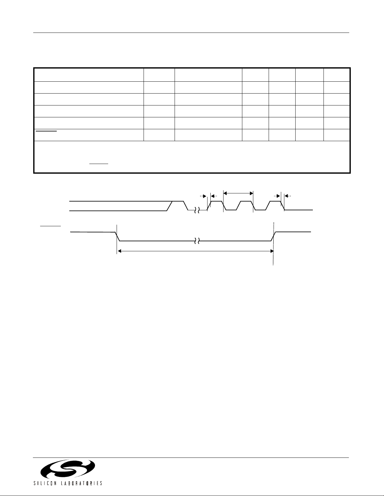
Table 6. Switching Characteristics—General Inputs
(VA, VD = 5 V ±5% or 3.3 V ±10%, TA = 70°C for K-grade, CL = 20 pF)
Si3000
Parameter
1
Cycle Time, MCLK t
MCLK Duty Cycle t
Rise Time, MCLK t
Fall Time, MCLK t
RESET
Notes:
Pulse Width
1. All timing (except Rise and Fall time) is referenced to the 50% level of the waveform. Input test levels are V
0.4 V, V
2.
The minimum RESET
2
= 0.4 V. Rise and Fall times are referenced to the 20% and 80% levels of the waveform.
IL
pulse width is the greater of 5 µs or 10 MCLK cycle times.
Symbol Test Condition Min Typ Max Unit
mc
dty
t
r
f
rl
t
r
16.67 — — ns
40 50 60 %
—— 5 ns
—— 5 ns
250 — — ns
t
mc
t
f
MCLK
RESET
IH
V
IH
V
IL
= VD –
t
rl
Figure 1. General Inputs Timing Diagram
Rev. 1.1 7
Si3000
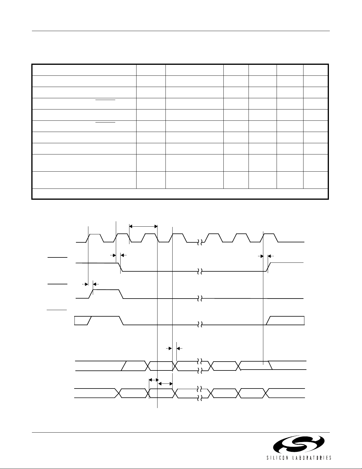
Table 7. Switching Characteristics—Serial Interface
(VA, VD = 5 V ±5% or 3.3 V ±10%, TA = 70°C for K-grade, CL = 20 pF)
Parameter Symbol Test Condition Min Typ Max Unit
Cycle Time, SCLK t
SCLK Duty Cycle t
Delay Time, SCLK ↑ to FSYNC
↓ t
Delay Time, SCLK ↑ to SDO Valid t
Delay Time, SCLK ↑ to FSYNC
↑ t
Setup Time, SDI, before SCLK ↓ t
Hold Time, SDI, after SCLK ↓ t
Setup Time, FSYNC (mode 2) before
c
dty
d1
d2
d3
su
h
t
su
354 1/256 Fs — ns
25 — — ns
20 — — ns
25 — — ns
MCLK ↓
Hold Time, FSYNC (mode 2) after
t
h
20 — — ns
MCLK ↓
Note: All timing is referenced to the 50% level of the waveform. Input test levels are V
t
c
SCLK
t
d1
FSYNC
(mode 0)
—50—%
— — 10 ns
— — 20 ns
— — 10 ns
= VD – 0.4 V, VIL = 0.4 V
IH
V
OH
V
OL
t
d3
t
FSYNC
(mode 1)
d3
FSYNC
(mode 2)
t
16-bit
SDO
16-bit
SDI
High-Z
D15
D15
D14
t
su
D14
... D2
t
h
... D2
Figure 2. Serial Interface Timing Diagram
8 Rev. 1.1
d2
D1
D1
D0
D0
High-Z
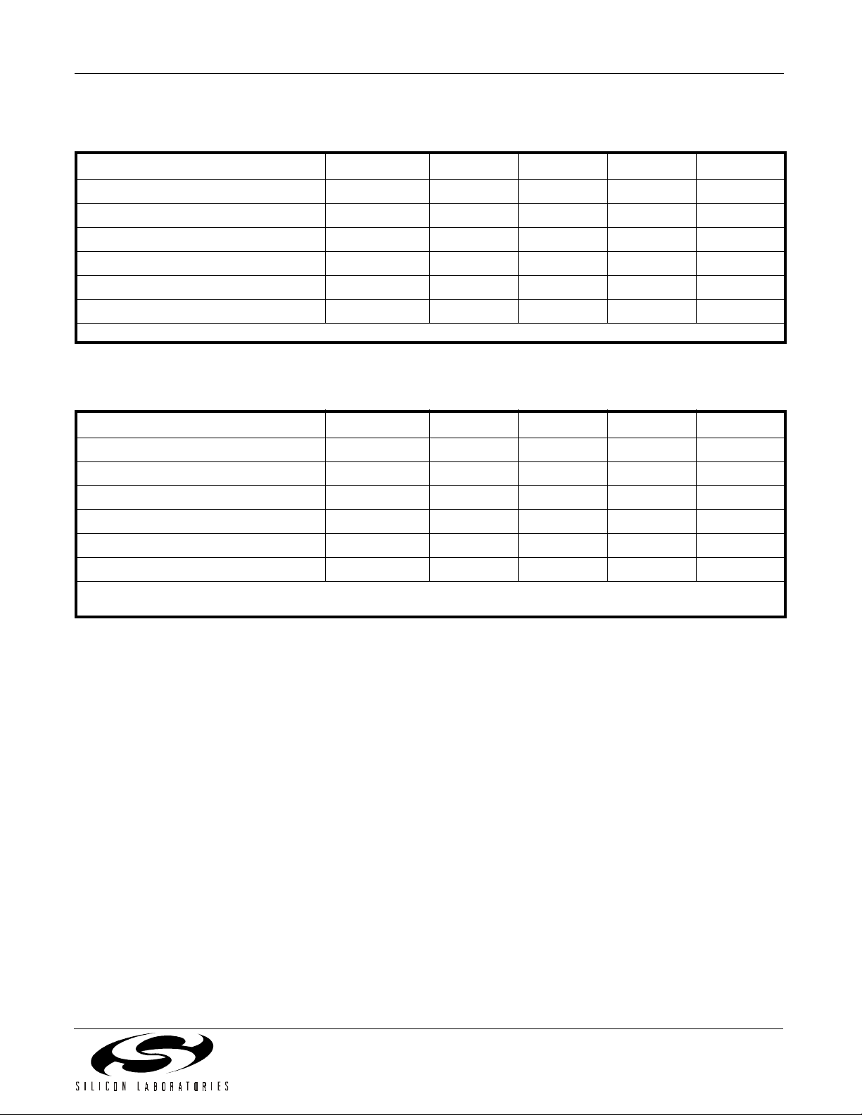
Table 8. Digital FIR Filter Characteristics—Transmit and Receive
(VA, VD = 5 V ±5% or 3.3 V ±10%, Sample Rate = 8 kHz, TA = 70°C for K-Grade)
Parameter Symbol Min Typ Max Unit
Si3000
Passband (3 dB, HPFD = 1)
Passband (3 dB, HPFD = 0)
F
(3 dB)
F
(3 dB)
Passband Ripple Peak-to-Peak
Stopband
Stopband Attenuation
Group Delay
Note:
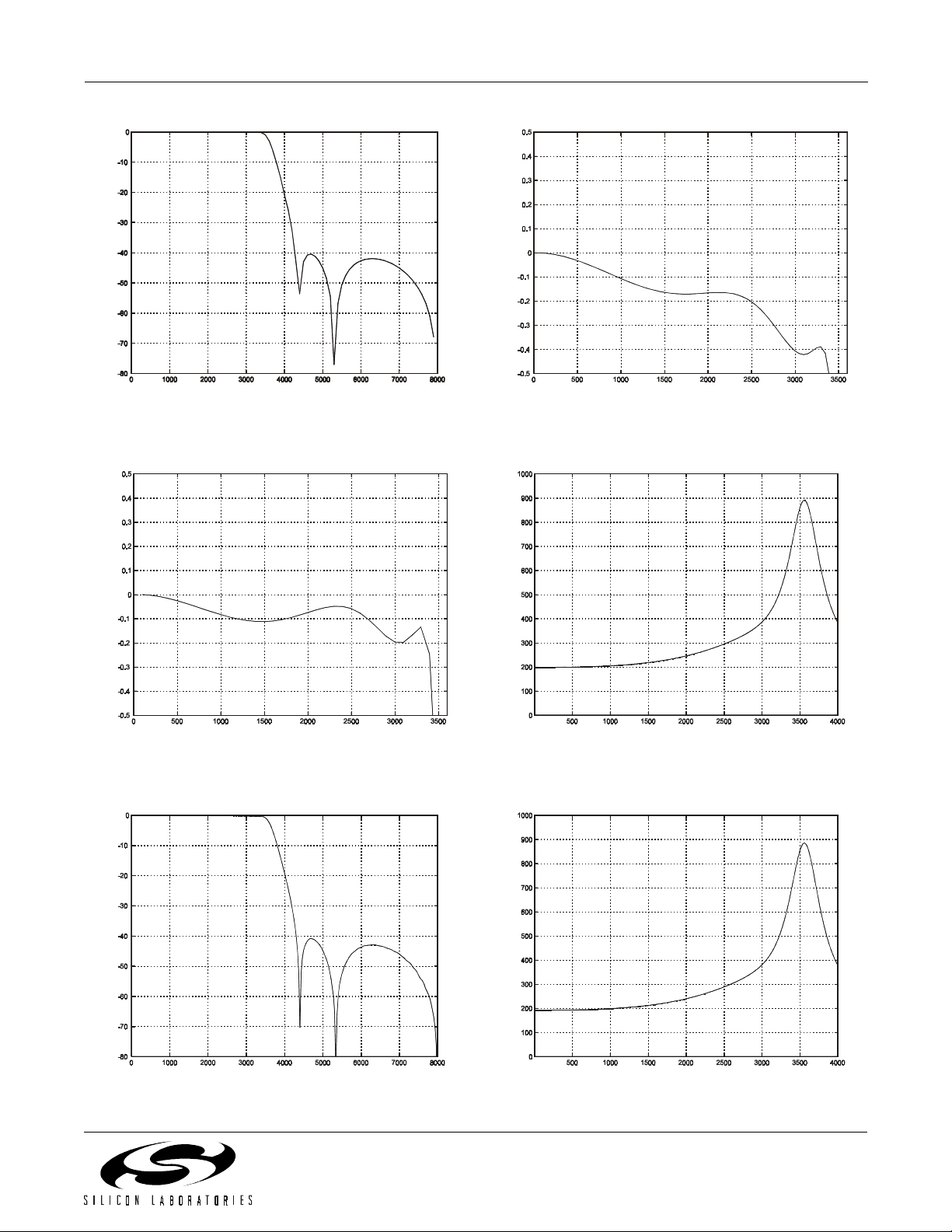
Typical FIR filter characteristics for Fs = 8000 Hz are shown in Figures 3, 4, 5, and 6.
t
gd
0—3.6kHz
0.01 — 3.6 kHz
–0.1 — 0.1 dB
—4.4—kHz
–74 — — dB
— 12/Fs — sec
Table 9. Digital IIR Filter Characteristics—Transmit and Receive
(VA, VD = 5 V ±5% or 3.3 V ±10%, Sample Rate = 8 kHz, TA = 70°C for K-Grade)
Parameter Symbol Min Typ Max Unit
Passband (3 dB, HPFD = 1)
Passband (3 dB, HPFD = 0)
F
(3 dB)
F
(3 dB)
Passband Ripple Peak-to-Peak
Stopband
Stopband Attenuation
Group Delay
Note: Typical IIR filter characteristics for Fs = 8000 Hz are shown in Figures 7, 8, 9, and 10. Figures 11 and 12 show group
delay versus input frequency.
t
gd
0—3.6kHz
0.01 — 3.6 kHz
–0.2 — 0.2 dB
—4.4—kHz
–40 — — dB
— 1.6/Fs — sec
Rev. 1.1 9

Si3000
Attenuation - dB
Input Frequency - Hz
Figure 3. FIR Receive Filter Response
Attenuation - dB
Input Frequency - Hz
Figure 4. FIR Receive Filter Passband Ripple
Attenuation - dB
Input Frequency - Hz
Figure 5. FIR Transmit Filter Response
Attenuation - dB
Input Frequency - Hz
Figure 6. FIR T ransmi t Filter Passband Ripple
For Figures 3–6, all filter plots apply to a sample rate of
Fs = 8 kHz. The filters scale with the sample rate as follows:
F
where Fs is the sample frequency.
10 Rev. 1.1
(0.1 dB)
F
(– 3 dB)
= 0.4125 Fs
= 0.45 Fs
Si3000
Attenuation - dB
Input Frequency - Hz
Figure 7. IIR Receive Filter Response
Attenuation - dB
Input Frequency - Hz
Figure 8. IIR Receive Filter Passband Ripple
Attenuation - dB
Input Frequency - Hz
Figure 10. IIR Transmit Filter Passband Ripple
Delay - µs
Input Frequency - Hz
Figure 11. IIR Receive Group Delay
Attenuation - dB
Input Frequency - Hz
Figure 9. IIR T ransmit Filter Response
Delay - µs
Input Frequency - Hz
Figure 12. IIR Transmit Group Delay
Rev. 1.1 11
 Loading...