

Page 1
AN93
UART
Interface
Parallel
Interface
DSP
DAA
Interface
ROM
PLL
Clocking
XTI XTO
CLKOUT
INT
RESET
C1
To Phone
Line
AOUT
Data Bus
Controller
Si3018/10
RXD
TXD
CTS
RTS
DCD
ESC
RI
CS
WR
RD
A0
D0-D7
Program Bus
RAM
EEPROM
Interface
EESD
EECLK
EECS
C2
Si3000
Interface
FSYNC
SDO
SDI
MCLK
SPI
Interface
SDI
SDO
SCLK
SS
AOUTb
Si2493/57/34/15/04 (Revision D) and Si2494/39
Modem Designer’s Guide
1. Introduction
The Si2494/93/57/39/34/15/04 ISOmodem chipset family consists of a 38-pin QFN (Si2494/39) or 24-pin TSSOP
(Si2493/57/34/15/04) or 16-pin SOIC (Si2493/57/34/15/04) low-voltage modem device, and a 16-pin SOIC lineside DAA device (Si3018/10) connecting directly with the telephone local loop (Tip and Ring). This modem solution
is a complete hardware (controller-based) modem that connects to a host processor through a UART, parallel or
SPI interface. Parallel and EEPROM interfaces are available only on the 38-pin QFN or 24-pin TSSOP package
option. Refer to Table 4, “ISOmodem Capabilities,” on page 10 for available part number, capability and package
combinations. Isolation is provided by Silicon Laboratories’ isolation capacitor technology, which uses high-voltage
capacitors instead of a transformer. This isolation technology complies with global telecommunications standards
including FCC, ETSI ES 203 021, JATE, and all known country-specific requirements.
Additional features include programmable ac/dc termination and ring impedance, on-hook and off-hook intrusion
detection, Caller ID, loop voltage/loop current monitoring, overcurrent detection, ring detection, and the hookswitch function. All required program and data memory is included in the modem device. When the modem
receives a software or hardware reset, all register settings revert to the default values stored in the on-chip
program memory. The host processor interacts with the modem controller through AT commands used to change
register settings and control modem operation. Country, EMI/EMC, and safety test reports are available from
Silicon Laboratories representatives and distributors.
This application note is intended to supplement the Si2494/39 Revision A, Si2493 Revision D, and the Si2457/34/
15/04 Revision D data sheets. It provides all the hardware and software information necessary to implement a
variety of modem applications, including reference schematics, sample PCB layouts, AT command and register
reference, country configuration tables, programming examples and more. Particular topics of interest can be
easily located through the table of contents or the comprehensive index located at the back of this document.
Rev. 1.3 8/11 Copyright © 2011 by Silicon Laboratories AN93
This information applies to a product under development. Its characteristics and specifications are subject to change without notice.
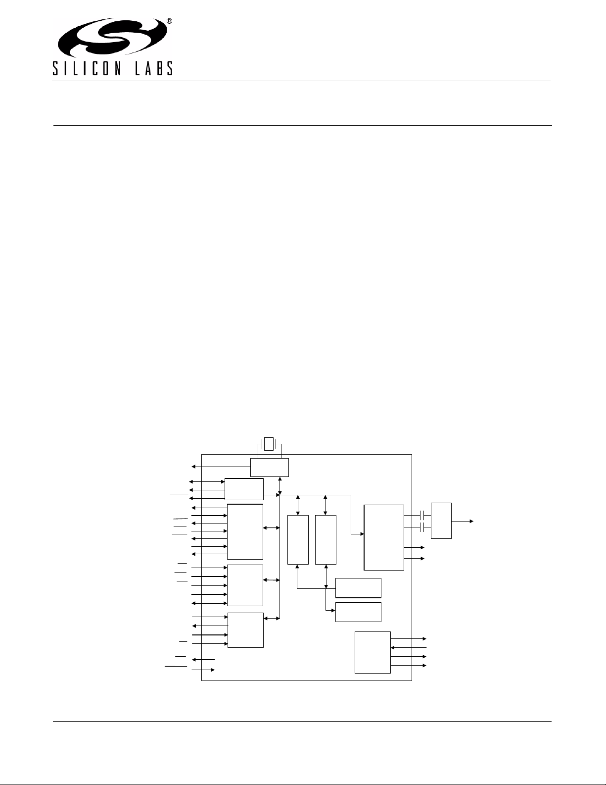
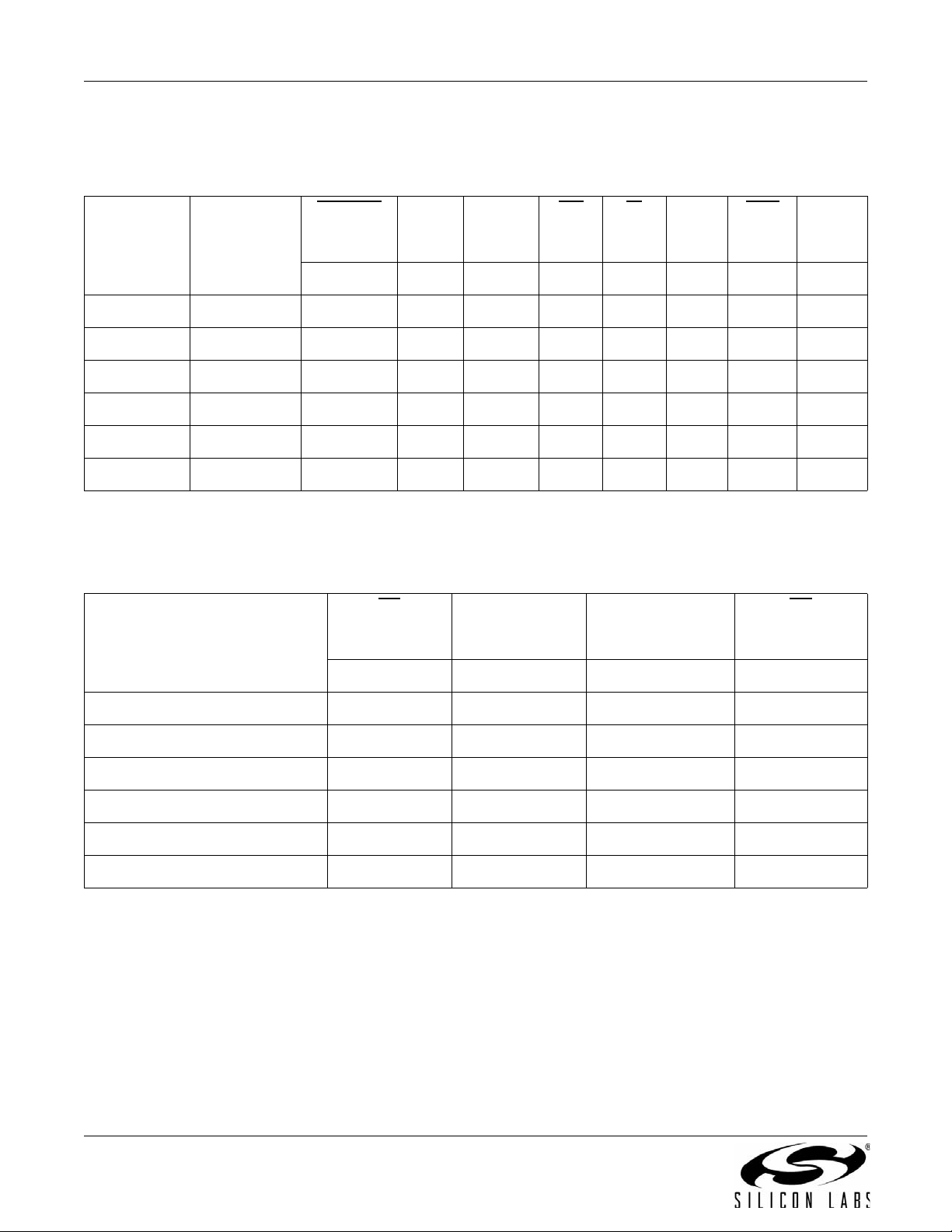
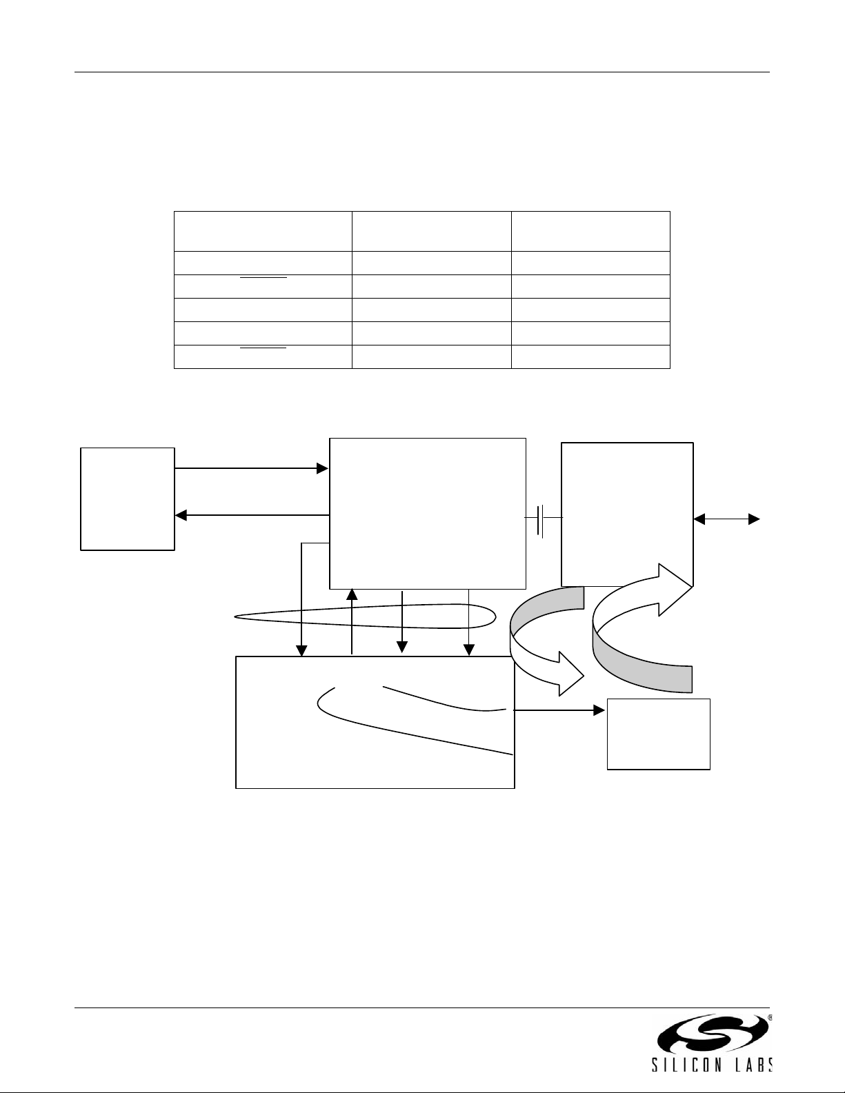
Figure 1. Functional Block Diagram
Page 2

AN93
2 Rev. 1.3
Page 3

AN93
TABLE OF CONTENTS
Section Page
1. Introduction . . . . . . . . . . . . . . . . . . . . . . . . . . . . . . . . . . . . . . . . . . . . . . . . . . . . . . . . . . . . . . 1
1.1. Selection Guide . . . . . . . . . . . . . . . . . . . . . . . . . . . . . . . . . . . . . . . . . . . . . . . . . . . . . . 9
2. Modem (System-Side) Device . . . . . . . . . . . . . . . . . . . . . . . . . . . . . . . . . . . . . . . . . . . . . . . 11
2.1. Resetting the Device . . . . . . . . . . . . . . . . . . . . . . . . . . . . . . . . . . . . . . . . . . . . . . . . . . 11
2.1.1. Reset Sequence. . . . . . . . . . . . . . . . . . . . . . . . . . . . . . . . . . . . . . . . . . . . . . . . 11
2.1.2. Reset Strapping: General Considerations . . . . . . . . . . . . . . . . . . . . . . . . . . . . 12
2.1.3. Reset-Strap Options for 16-Pin SOIC Package . . . . . . . . . . . . . . . . . . . . . . . . 13
2.1.4. Reset-Strap Options for 24-Pin TSSOP Package . . . . . . . . . . . . . . . . . . . . . . 13
2.1.4.1. Reset Strapping Options for TSSOP-24 with UART-Interface. . . . . . . . . 14
2.1.4.2. Reset Strapping Options for TSSOP-24 with Parallel-Interface. . . . . . . . 14
2.1.4.3. Reset Strapping Options for TSSOP with SPI-Interface . . . . . . . . . . . . . 15
2.1.5. Reset Strapping Options for QFN Parts. . . . . . . . . . . . . . . . . . . . . . . . . . . . . . 15
2.1.5.1. Reset Strapping Options for QFN Parts with UART Operation . . . . . . . . 15
2.1.5.2. Reset Strapping Options for QFN Parts with SPI Operation . . . . . . . . . . 16
2.1.5.3. Reset Strapping Options for QFN Parts with Parallel Operation . . . . . . . 16
2.2. System Interface . . . . . . . . . . . . . . . . . . . . . . . . . . . . . . . . . . . . . . . . . . . . . . . . . . . . . 17
2.2.1. Interface Selection . . . . . . . . . . . . . . . . . . . . . . . . . . . . . . . . . . . . . . . . . . . . . . 17
2.2.2. Interface Signal Description . . . . . . . . . . . . . . . . . . . . . . . . . . . . . . . . . . . . . . . 19
2.2.3. UART Interface Operation . . . . . . . . . . . . . . . . . . . . . . . . . . . . . . . . . . . . . . . . 19
2.2.3.1. UART Options . . . . . . . . . . . . . . . . . . . . . . . . . . . . . . . . . . . . . . . . . . . . . 19
2.2.3.2. Autobaud . . . . . . . . . . . . . . . . . . . . . . . . . . . . . . . . . . . . . . . . . . . . . . . . . 20
2.2.3.3. Flow Control. . . . . . . . . . . . . . . . . . . . . . . . . . . . . . . . . . . . . . . . . . . . . . . 21
2.2.4. Parallel and SPI Interface Operation . . . . . . . . . . . . . . . . . . . . . . . . . . . . . . . . 23
2.2.4.1. Hardware Interface Register 0. . . . . . . . . . . . . . . . . . . . . . . . . . . . . . . . . 25
2.2.4.2. Hardware Interface Register 1. . . . . . . . . . . . . . . . . . . . . . . . . . . . . . . . . 25
2.2.4.3. Parallel Interface Operation. . . . . . . . . . . . . . . . . . . . . . . . . . . . . . . . . . . 26
2.2.4.4. SPI Interface Operation . . . . . . . . . . . . . . . . . . . . . . . . . . . . . . . . . . . . . . 28
2.2.4.5. Interface Communication Modes. . . . . . . . . . . . . . . . . . . . . . . . . . . . . . . 28
2.3. Isolation Capacitor Interface . . . . . . . . . . . . . . . . . . . . . . . . . . . . . . . . . . . . . . . . . . . . 29
2.4. Low-Power Modes . . . . . . . . . . . . . . . . . . . . . . . . . . . . . . . . . . . . . . . . . . . . . . . . . . . 29
2.4.1. Power-Down Mode. . . . . . . . . . . . . . . . . . . . . . . . . . . . . . . . . . . . . . . . . . . . . . 29
2.4.2. Wake-on-Ring Mode. . . . . . . . . . . . . . . . . . . . . . . . . . . . . . . . . . . . . . . . . . . . . 29
2.4.3. Sleep Mode . . . . . . . . . . . . . . . . . . . . . . . . . . . . . . . . . . . . . . . . . . . . . . . . . . . 29
2.5. SSI/Voice Mode (24-Pin TSSOP and 38-Pin QFN Only) . . . . . . . . . . . . . . . . . . . . . . 30
2.6. EEPROM Interface (24-Pin TSSOP and 38-Pin QFN Only) . . . . . . . . . . . . . . . . . . . . 31
2.6.1. Supported EEPROM Types . . . . . . . . . . . . . . . . . . . . . . . . . . . . . . . . . . . . . . . 31
2.6.2. Three-Wire SPI Interface to EEPROM. . . . . . . . . . . . . . . . . . . . . . . . . . . . . . . 33
2.6.3. Detailed EEPROM Examples. . . . . . . . . . . . . . . . . . . . . . . . . . . . . . . . . . . . . . 33
2.6.4. Boot Commands (Custom Defaults) . . . . . . . . . . . . . . . . . . . . . . . . . . . . . . . . . 33
2.6.5. AT Command Macros (Customized AT Commands) . . . . . . . . . . . . . . . . . . . . 34
2.6.6. Firmware Upgrades . . . . . . . . . . . . . . . . . . . . . . . . . . . . . . . . . . . . . . . . . . . . . 34
2.6.6.1. Boot Command Example. . . . . . . . . . . . . . . . . . . . . . . . . . . . . . . . . . . . . 34
Rev. 1.3 3
Page 4

AN93
2.6.6.2. AT Command Macro Example. . . . . . . . . . . . . . . . . . . . . . . . . . . . . . . . . 35
2.6.6.3. Autoloading Firmware Upgrade Example . . . . . . . . . . . . . . . . . . . . . . . . 35
2.6.6.4. Combination Example . . . . . . . . . . . . . . . . . . . . . . . . . . . . . . . . . . . . . . . 36
3. DAA (Line-Side) Device . . . . . . . . . . . . . . . . . . . . . . . . . . . . . . . . . . . . . . . . . . . . . . . . . . . . 38
3.1. Hookswitch and DC Termination . . . . . . . . . . . . . . . . . . . . . . . . . . . . . . . . . . . . . . . . 38
3.2. AC Termination . . . . . . . . . . . . . . . . . . . . . . . . . . . . . . . . . . . . . . . . . . . . . . . . . . . . . . 39
3.3. Ringer Impedance and Threshold . . . . . . . . . . . . . . . . . . . . . . . . . . . . . . . . . . . . . . . 39
3.4. Pulse Dialing and Spark Quenching . . . . . . . . . . . . . . . . . . . . . . . . . . . . . . . . . . . . . . 39
3.5. Line Voltage and Loop Current Sensing . . . . . . . . . . . . . . . . . . . . . . . . . . . . . . . . . . . 39
3.6. Legacy-Mode Line Voltage and Loop Current Measurement . . . . . . . . . . . . . . . . . . . 42
3.7. Billing Tone Detection . . . . . . . . . . . . . . . . . . . . . . . . . . . . . . . . . . . . . . . . . . . . . . . . . 42
4. Hardware Design Reference . . . . . . . . . . . . . . . . . . . . . . . . . . . . . . . . . . . . . . . . . . . . . . . . 43
4.1. Component Functions . . . . . . . . . . . . . . . . . . . . . . . . . . . . . . . . . . . . . . . . . . . . . . . . . 43
4.1.1. Power Supply and Bias Circuitry . . . . . . . . . . . . . . . . . . . . . . . . . . . . . . . . . . . 43
4.1.2. Hookswitch and DC Termination . . . . . . . . . . . . . . . . . . . . . . . . . . . . . . . . . . . 43
4.1.3. Clocks. . . . . . . . . . . . . . . . . . . . . . . . . . . . . . . . . . . . . . . . . . . . . . . . . . . . . . . . 43
4.1.4. Ringer Network. . . . . . . . . . . . . . . . . . . . . . . . . . . . . . . . . . . . . . . . . . . . . . . . . 44
4.1.5. Optional Billing-Tone Filter. . . . . . . . . . . . . . . . . . . . . . . . . . . . . . . . . . . . . . . . 44
4.2. Schematic . . . . . . . . . . . . . . . . . . . . . . . . . . . . . . . . . . . . . . . . . . . . . . . . . . . . . . . . . . 47
4.3. Bill of Materials . . . . . . . . . . . . . . . . . . . . . . . . . . . . . . . . . . . . . . . . . . . . . . . . . . . . . . 48
4.4. Layout Guidelines . . . . . . . . . . . . . . . . . . . . . . . . . . . . . . . . . . . . . . . . . . . . . . . . . . . . 49
4.4.1. ISOmodem Layout Check List . . . . . . . . . . . . . . . . . . . . . . . . . . . . . . . . . . . . . 51
4.4.2. Module Design and Application Considerations. . . . . . . . . . . . . . . . . . . . . . . . 53
4.4.2.1. Module Design. . . . . . . . . . . . . . . . . . . . . . . . . . . . . . . . . . . . . . . . . . . . . 53
4.4.2.2. Motherboard Design . . . . . . . . . . . . . . . . . . . . . . . . . . . . . . . . . . . . . . . . 53
4.5. Analog Output . . . . . . . . . . . . . . . . . . . . . . . . . . . . . . . . . . . . . . . . . . . . . . . . . . . . . . . 54
4.5.1. Interaction between the AOUT Circuit and the
Required Modem Reset Time . . . . . . . . . . . . . . . . . . . . . . . . . . . . . . . . . . . . . 54
4.5.2. Audio Quality . . . . . . . . . . . . . . . . . . . . . . . . . . . . . . . . . . . . . . . . . . . . . . . . . . 55
5. Modem Reference Guide . . . . . . . . . . . . . . . . . . . . . . . . . . . . . . . . . . . . . . . . . . . . . . . . . . . 56
5.1. Controller . . . . . . . . . . . . . . . . . . . . . . . . . . . . . . . . . . . . . . . . . . . . . . . . . . . . . . . . . . 56
5.2. DSP . . . . . . . . . . . . . . . . . . . . . . . . . . . . . . . . . . . . . . . . . . . . . . . . . . . . . . . . . . . . . . 57
5.3. Memory . . . . . . . . . . . . . . . . . . . . . . . . . . . . . . . . . . . . . . . . . . . . . . . . . . . . . . . . . . . . 57
5.4. AT Command Set . . . . . . . . . . . . . . . . . . . . . . . . . . . . . . . . . . . . . . . . . . . . . . . . . . . . 57
5.5. Extended AT Commands . . . . . . . . . . . . . . . . . . . . . . . . . . . . . . . . . . . . . . . . . . . . . . 77
5.6. S Registers . . . . . . . . . . . . . . . . . . . . . . . . . . . . . . . . . . . . . . . . . . . . . . . . . . . . . . . . . 88
5.7. U Registers . . . . . . . . . . . . . . . . . . . . . . . . . . . . . . . . . . . . . . . . . . . . . . . . . . . . . . . . . 91
5.7.1. U-Register Summary . . . . . . . . . . . . . . . . . . . . . . . . . . . . . . . . . . . . . . . . . . . . 96
5.7.2. U00–U16 (Dial Tone Detect Filter Registers). . . . . . . . . . . . . . . . . . . . . . . . . . 97
5.7.3. U17–U30 (Busy Tone Detect Filter Registers). . . . . . . . . . . . . . . . . . . . . . . . . 98
5.7.4. U31–U33 (Ringback Cadence Registers) . . . . . . . . . . . . . . . . . . . . . . . . . . . 101
5.7.5. U34–U35 (Dial Tone Timing Register) . . . . . . . . . . . . . . . . . . . . . . . . . . . . . . 101
5.7.6. U37–U45 (Pulse Dial Registers). . . . . . . . . . . . . . . . . . . . . . . . . . . . . . . . . . . 101
5.7.7. U46–U48 (DTMF Dial Registers) . . . . . . . . . . . . . . . . . . . . . . . . . . . . . . . . . . 102
5.7.8. U49–U4C (Ring Detect Registers) . . . . . . . . . . . . . . . . . . . . . . . . . . . . . . . . . 103
5.7.9. U4D (Modem Control Register 1—MOD1). . . . . . . . . . . . . . . . . . . . . . . . . . . 103
5.7.10. U4E (Pre-Dial Delay Time Register). . . . . . . . . . . . . . . . . . . . . . . . . . . . . . . 105
4 Rev. 1.3
Page 5

AN93
5.7.11. U4F (Flash Hook Time Register) . . . . . . . . . . . . . . . . . . . . . . . . . . . . . . . . . 105
5.7.12. U50–U51 (Loop Current Debouncing Registers) . . . . . . . . . . . . . . . . . . . . . 105
5.7.13. U52 (Transmit Level Register) . . . . . . . . . . . . . . . . . . . . . . . . . . . . . . . . . . . 105
5.7.14. U53 (Modem Control Register 2) . . . . . . . . . . . . . . . . . . . . . . . . . . . . . . . . . 106
5.7.15. U54 (Calibration Timing Register) . . . . . . . . . . . . . . . . . . . . . . . . . . . . . . . . 106
5.7.16. U62–U66 (DAA Control Registers). . . . . . . . . . . . . . . . . . . . . . . . . . . . . . . . 106
5.7.17. U67–U6A (International Configuration Registers) . . . . . . . . . . . . . . . . . . . . 108
5.7.18. U6C (Line-Voltage Status Register). . . . . . . . . . . . . . . . . . . . . . . . . . . . . . . 111
5.7.19. U6E–U7D (Modem Control and Interface Registers). . . . . . . . . . . . . . . . . . 111
5.7.20. U80 (Transmit Delay for V.22 Fast Connect) . . . . . . . . . . . . . . . . . . . . . . . . 119
5.7.21. U87 (Synchronous Access Mode Configuration Register) . . . . . . . . . . . . . . 120
5.7.22. UAA (V.29 Mode Register). . . . . . . . . . . . . . . . . . . . . . . . . . . . . . . . . . . . . . 121
5.7.23. UIDA Response and Answer Tone Delay Register . . . . . . . . . . . . . . . . . . . 121
5.8. Firmware Upgrades . . . . . . . . . . . . . . . . . . . . . . . . . . . . . . . . . . . . . . . . . . . . . . . . . 121
5.8.1. Method 1 (Fastest) . . . . . . . . . . . . . . . . . . . . . . . . . . . . . . . . . . . . . . . . . . . . . 121
5.8.2. Method 2. . . . . . . . . . . . . . . . . . . . . . . . . . . . . . . . . . . . . . . . . . . . . . . . . . . . . 122
5.8.3. Method 3. . . . . . . . . . . . . . . . . . . . . . . . . . . . . . . . . . . . . . . . . . . . . . . . . . . . . 122
5.9. Escape Methods . . . . . . . . . . . . . . . . . . . . . . . . . . . . . . . . . . . . . . . . . . . . . . . . . . . . 122
5.9.1. +++ Escape . . . . . . . . . . . . . . . . . . . . . . . . . . . . . . . . . . . . . . . . . . . . . . . . . . 123
5.9.2. “9th Bit” Escape . . . . . . . . . . . . . . . . . . . . . . . . . . . . . . . . . . . . . . . . . . . . . . . 123
5.9.3. “Escape Pin” Escape . . . . . . . . . . . . . . . . . . . . . . . . . . . . . . . . . . . . . . . . . . . 123
5.10. Data Compression . . . . . . . . . . . . . . . . . . . . . . . . . . . . . . . . . . . . . . . . . . . . . . . . . 124
5.11. Error Correction . . . . . . . . . . . . . . . . . . . . . . . . . . . . . . . . . . . . . . . . . . . . . . . . . . . 124
5.12. Wire Mode . . . . . . . . . . . . . . . . . . . . . . . . . . . . . . . . . . . . . . . . . . . . . . . . . . . . . . . 124
5.13. EPOS (Electronic Point of Sale) Applications . . . . . . . . . . . . . . . . . . . . . . . . . . . . . 125
5.13.1. EPOS Fast Connect. . . . . . . . . . . . . . . . . . . . . . . . . . . . . . . . . . . . . . . . . . . 125
5.13.2. EPOS V.29 Fast Connect. . . . . . . . . . . . . . . . . . . . . . . . . . . . . . . . . . . . . . . 125
5.14. Legacy Synchronous DCE Mode/V.80 Synchronous Access Mode . . . . . . . . . . . . 125
5.15. V.80 Mode . . . . . . . . . . . . . . . . . . . . . . . . . . . . . . . . . . . . . . . . . . . . . . . . . . . . . . . 125
6. Programming Examples . . . . . . . . . . . . . . . . . . . . . . . . . . . . . . . . . . . . . . . . . . . . . . . . . . 132
6.1. Quick Reference . . . . . . . . . . . . . . . . . . . . . . . . . . . . . . . . . . . . . . . . . . . . . . . . . . . . 132
6.2. Country-Dependent Setup . . . . . . . . . . . . . . . . . . . . . . . . . . . . . . . . . . . . . . . . . . . . 133
6.2.1. DC Termination . . . . . . . . . . . . . . . . . . . . . . . . . . . . . . . . . . . . . . . . . . . . . . . 133
6.2.2. Country Configuration. . . . . . . . . . . . . . . . . . . . . . . . . . . . . . . . . . . . . . . . . . . 134
6.2.2.1. Country Initialization Table. . . . . . . . . . . . . . . . . . . . . . . . . . . . . . . . . . . 134
6.2.2.2. Country-Setting Register Tables . . . . . . . . . . . . . . . . . . . . . . . . . . . . . . 145
6.2.2.3. Special Requirements for India . . . . . . . . . . . . . . . . . . . . . . . . . . . . . . . 146
6.2.2.4. Special Requirements for Serbia and Montenegro . . . . . . . . . . . . . . . . 147
6.2.3. Blacklisting . . . . . . . . . . . . . . . . . . . . . . . . . . . . . . . . . . . . . . . . . . . . . . . . . . . 147
6.3. Caller ID . . . . . . . . . . . . . . . . . . . . . . . . . . . . . . . . . . . . . . . . . . . . . . . . . . . . . . . . . . 148
6.3.1. Force Caller ID Monitor (Always On) . . . . . . . . . . . . . . . . . . . . . . . . . . . . . . . 148
6.3.2. Caller ID After Ring Only . . . . . . . . . . . . . . . . . . . . . . . . . . . . . . . . . . . . . . . . 148
6.3.3. UK Caller ID with Wetting Pulse. . . . . . . . . . . . . . . . . . . . . . . . . . . . . . . . . . . 148
6.3.4. Japan Caller ID . . . . . . . . . . . . . . . . . . . . . . . . . . . . . . . . . . . . . . . . . . . . . . . . 148
6.3.5. DTMF Caller ID. . . . . . . . . . . . . . . . . . . . . . . . . . . . . . . . . . . . . . . . . . . . . . . . 149
6.4. SMS Support . . . . . . . . . . . . . . . . . . . . . . . . . . . . . . . . . . . . . . . . . . . . . . . . . . . . . . 149
6.5. Type II Caller ID/SAS Detection . . . . . . . . . . . . . . . . . . . . . . . . . . . . . . . . . . . . . . . . 151
Rev. 1.3 5
Page 6

AN93
6.6. Intrusion/Parallel Phone Detection . . . . . . . . . . . . . . . . . . . . . . . . . . . . . . . . . . . . . . 161
6.6.1. On-Hook Condition. . . . . . . . . . . . . . . . . . . . . . . . . . . . . . . . . . . . . . . . . . . . . 161
6.6.1.1. Line Not Present/In Use Indication (Method 1—Fixed) . . . . . . . . . . . . . 161
6.6.1.2. Line Not Present/In Use Indication (Method 2—Adaptive). . . . . . . . . . . 162
6.6.2. Off-Hook Condition. . . . . . . . . . . . . . . . . . . . . . . . . . . . . . . . . . . . . . . . . . . . . 162
6.7. Modem-On-Hold . . . . . . . . . . . . . . . . . . . . . . . . . . . . . . . . . . . . . . . . . . . . . . . . . . . . 164
6.7.1. Initiating Modem-On-Hold. . . . . . . . . . . . . . . . . . . . . . . . . . . . . . . . . . . . . . . . 164
6.7.2. Receiving Modem-On-Hold Requests . . . . . . . . . . . . . . . . . . . . . . . . . . . . . . 165
6.8. HDLC: Bit Errors on a Noisy Line . . . . . . . . . . . . . . . . . . . . . . . . . . . . . . . . . . . . . . . 165
6.9. Overcurrent Detection . . . . . . . . . . . . . . . . . . . . . . . . . . . . . . . . . . . . . . . . . . . . . . . . 169
6.10. Pulse/Tone Dial Decision . . . . . . . . . . . . . . . . . . . . . . . . . . . . . . . . . . . . . . . . . . . . 169
6.10.1. Method 1: Multiple Off-Hook Transitions. . . . . . . . . . . . . . . . . . . . . . . . . 169
6.10.2. Method 2: Single Off-Hook Transition . . . . . . . . . . . . . . . . . . . . . . . . . . . 170
6.10.3. Method 3: Adaptive Dialing. . . . . . . . . . . . . . . . . . . . . . . . . . . . . . . . . . . . . . 170
6.10.4. Automatic Phone-Line Configuration Detection . . . . . . . . . . . . . . . . . . . . . . 170
6.10.5. Line Type Determination . . . . . . . . . . . . . . . . . . . . . . . . . . . . . . . . . . . . . . . 170
6.11. Telephone Voting Mode . . . . . . . . . . . . . . . . . . . . . . . . . . . . . . . . . . . . . . . . . . . . . 171
6.12. V.92 Quick Connect . . . . . . . . . . . . . . . . . . . . . . . . . . . . . . . . . . . . . . . . . . . . . . . . 171
7. Handset, TAM, and Speakerphone Operation . . . . . . . . . . . . . . . . . . . . . . . . . . . . . . . . . 173
7.1. Software Reference . . . . . . . . . . . . . . . . . . . . . . . . . . . . . . . . . . . . . . . . . . . . . . . . . 173
7.1.1. AT Command Set. . . . . . . . . . . . . . . . . . . . . . . . . . . . . . . . . . . . . . . . . . . . . . 173
7.1.2. AT+ Extended Commands. . . . . . . . . . . . . . . . . . . . . . . . . . . . . . . . . . . . . . . 173
7.1.3. <DLE> Commands (DTE-to-DCE) . . . . . . . . . . . . . . . . . . . . . . . . . . . . . . . . . 178
7.1.4. <DLE> Events (DCE-to-DTE). . . . . . . . . . . . . . . . . . . . . . . . . . . . . . . . . . . . . 179
7.1.4.1. Simple Event Reporting . . . . . . . . . . . . . . . . . . . . . . . . . . . . . . . . . . . . . 179
7.1.4.2. Complex Event Reporting . . . . . . . . . . . . . . . . . . . . . . . . . . . . . . . . . . . 181
7.1.5. U Registers. . . . . . . . . . . . . . . . . . . . . . . . . . . . . . . . . . . . . . . . . . . . . . . . . . . 181
7.2. Voice Reference—Overview . . . . . . . . . . . . . . . . . . . . . . . . . . . . . . . . . . . . . . . . . . . 187
7.3. Si3000 Configuration . . . . . . . . . . . . . . . . . . . . . . . . . . . . . . . . . . . . . . . . . . . . . . . . 192
7.3.1. Microphone and Speaker Ports . . . . . . . . . . . . . . . . . . . . . . . . . . . . . . . . . . . 192
7.3.2. Register Settings . . . . . . . . . . . . . . . . . . . . . . . . . . . . . . . . . . . . . . . . . . . . . . 192
7.3.3. System Voice Modes . . . . . . . . . . . . . . . . . . . . . . . . . . . . . . . . . . . . . . . . . . . 192
7.3.3.1. TAM Hands-Free . . . . . . . . . . . . . . . . . . . . . . . . . . . . . . . . . . . . . . . . . . 192
7.3.3.2. TAM Handset. . . . . . . . . . . . . . . . . . . . . . . . . . . . . . . . . . . . . . . . . . . . . 192
7.3.3.3. Speakerphone . . . . . . . . . . . . . . . . . . . . . . . . . . . . . . . . . . . . . . . . . . . . 192
7.3.3.4. Handset . . . . . . . . . . . . . . . . . . . . . . . . . . . . . . . . . . . . . . . . . . . . . . . . . 192
7.3.3.5. TAM PSTN. . . . . . . . . . . . . . . . . . . . . . . . . . . . . . . . . . . . . . . . . . . . . . . 193
7.4. Initialization . . . . . . . . . . . . . . . . . . . . . . . . . . . . . . . . . . . . . . . . . . . . . . . . . . . . . . . . 194
7.5. Handset . . . . . . . . . . . . . . . . . . . . . . . . . . . . . . . . . . . . . . . . . . . . . . . . . . . . . . . . . . 196
7.5.1. Overview. . . . . . . . . . . . . . . . . . . . . . . . . . . . . . . . . . . . . . . . . . . . . . . . . . . . . 196
7.5.2. Handset Configuration . . . . . . . . . . . . . . . . . . . . . . . . . . . . . . . . . . . . . . . . . . 196
7.5.3. Call – Automatic Tone Dial. . . . . . . . . . . . . . . . . . . . . . . . . . . . . . . . . . . . . . . 198
7.5.4. Call – Manual Off-Hook Tone Dial . . . . . . . . . . . . . . . . . . . . . . . . . . . . . . . . . 198
7.5.5. Call – Automatic Pulse Dial . . . . . . . . . . . . . . . . . . . . . . . . . . . . . . . . . . . . . . 198
7.5.6. Answer . . . . . . . . . . . . . . . . . . . . . . . . . . . . . . . . . . . . . . . . . . . . . . . . . . . . . . 198
7.5.7. Terminate . . . . . . . . . . . . . . . . . . . . . . . . . . . . . . . . . . . . . . . . . . . . . . . . . . . . 199
6 Rev. 1.3
Page 7

AN93
7.5.8. Speakerphone Transition . . . . . . . . . . . . . . . . . . . . . . . . . . . . . . . . . . . . . . . . 200
7.6. Telephone Answering Machine . . . . . . . . . . . . . . . . . . . . . . . . . . . . . . . . . . . . . . . . 201
7.6.1. Overview. . . . . . . . . . . . . . . . . . . . . . . . . . . . . . . . . . . . . . . . . . . . . . . . . . . . . 201
7.6.2. TAM Hands-Free—Idle. . . . . . . . . . . . . . . . . . . . . . . . . . . . . . . . . . . . . . . . . . 201
7.6.2.1. Record OGM . . . . . . . . . . . . . . . . . . . . . . . . . . . . . . . . . . . . . . . . . . . . . 202
7.6.2.2. Review OGM . . . . . . . . . . . . . . . . . . . . . . . . . . . . . . . . . . . . . . . . . . . . . 203
7.6.2.3. Record Local ICM . . . . . . . . . . . . . . . . . . . . . . . . . . . . . . . . . . . . . . . . . 203
7.6.2.4. Review ICM . . . . . . . . . . . . . . . . . . . . . . . . . . . . . . . . . . . . . . . . . . . . . . 203
7.6.2.5. Speakerphone Transition. . . . . . . . . . . . . . . . . . . . . . . . . . . . . . . . . . . . 203
7.6.2.6. Handset Transition. . . . . . . . . . . . . . . . . . . . . . . . . . . . . . . . . . . . . . . . . 203
7.6.3. TAM Handset . . . . . . . . . . . . . . . . . . . . . . . . . . . . . . . . . . . . . . . . . . . . . . . . . 203
7.6.3.1. Record OGM . . . . . . . . . . . . . . . . . . . . . . . . . . . . . . . . . . . . . . . . . . . . . 203
7.6.3.2. Review OGM . . . . . . . . . . . . . . . . . . . . . . . . . . . . . . . . . . . . . . . . . . . . . 206
7.6.3.3. Record Local ICM . . . . . . . . . . . . . . . . . . . . . . . . . . . . . . . . . . . . . . . . . 208
7.6.3.4. Review ICM . . . . . . . . . . . . . . . . . . . . . . . . . . . . . . . . . . . . . . . . . . . . . . 208
7.6.4. TAM PSTN . . . . . . . . . . . . . . . . . . . . . . . . . . . . . . . . . . . . . . . . . . . . . . . . . . . 208
7.6.4.1. Normal Answer – OGM Playback with ICM Record. . . . . . . . . . . . . . . . 208
7.6.4.2. Interrupted Answer – OGM Playback with DTMF Menu Entry. . . . . . . . 210
7.6.4.3. Speakerphone Transition. . . . . . . . . . . . . . . . . . . . . . . . . . . . . . . . . . . . 212
7.6.4.4. Handset Transition. . . . . . . . . . . . . . . . . . . . . . . . . . . . . . . . . . . . . . . . . 212
7.7. Speakerphone . . . . . . . . . . . . . . . . . . . . . . . . . . . . . . . . . . . . . . . . . . . . . . . . . . . . . 212
7.7.1. Overview . . . . . . . . . . . . . . . . . . . . . . . . . . . . . . . . . . . . . . . . . . . . . . . . . . . . 212
7.7.2. Simplex Speakerphone . . . . . . . . . . . . . . . . . . . . . . . . . . . . . . . . . . . . . . . . . 212
7.7.3. External Microphone/Speaker Calibration . . . . . . . . . . . . . . . . . . . . . . . . . . . 213
7.7.3.1. Transmit Gain Calibration—Speakerphone Dis abled . . . . . . . . . . . . . . 213
7.7.3.2. Receive Gain Calibration—Speakerphone Disabled . . . . . . . . . . . . . . . 216
7.7.3.3. Speakerphone Calibration—AEC Gain Calibration . . . . . . . . . . . . . . . . 217
7.7.4. Speakerphone Configuration . . . . . . . . . . . . . . . . . . . . . . . . . . . . . . . . . . . . . 219
7.7.5. Simplex Speakerphone Configuration . . . . . . . . . . . . . . . . . . . . . . . . . . . . . . 220
7.7.6. Call—Automatic Tone Dial . . . . . . . . . . . . . . . . . . . . . . . . . . . . . . . . . . . . . . . 221
7.7.7. Call—Manual Off-Hook Tone Dial . . . . . . . . . . . . . . . . . . . . . . . . . . . . . . . . . 221
7.7.8. Call—Automatic Pulse Dial. . . . . . . . . . . . . . . . . . . . . . . . . . . . . . . . . . . . . . . 222
7.7.9. Answer . . . . . . . . . . . . . . . . . . . . . . . . . . . . . . . . . . . . . . . . . . . . . . . . . . . . . . 222
7.7.10. Handset Transition . . . . . . . . . . . . . . . . . . . . . . . . . . . . . . . . . . . . . . . . . . . . 222
7.7.11. Termination. . . . . . . . . . . . . . . . . . . . . . . . . . . . . . . . . . . . . . . . . . . . . . . . . . 223
7.8. Glossary . . . . . . . . . . . . . . . . . . . . . . . . . . . . . . . . . . . . . . . . . . . . . . . . . . . . . . . . . . 223
7.9. References . . . . . . . . . . . . . . . . . . . . . . . . . . . . . . . . . . . . . . . . . . . . . . . . . . . . . . . . 223
8. Security Protocols . . . . . . . . . . . . . . . . . . . . . . . . . . . . . . . . . . . . . . . . . . . . . . . . . . . . . . . 224
8.1. Implementing the SIA Protocol . . . . . . . . . . . . . . . . . . . . . . . . . . . . . . . . . . . . . . . . . 224
8.1.1. Modem-Specific Implementation Details . . . . . . . . . . . . . . . . . . . . . . . . . . . . 224
8.1.1.1. Listen-In and V-channel Periods (Voice Pass-Through) . . . . . . . . . . . . 224
8.1.1.2. Inserting a V.32bis period (e.g., SIA Level-3 Video Block Support). . . . 224
8.1.1.3. Considerations when Disconnecting the Session . . . . . . . . . . . . . . . . . 225
8.2. Implementing the Ademco® Contact ID Protocol . . . . . . . . . . . . . . . . . . . . . . . . . . . 228
8.2.1. Modem Specific Implementation Details . . . . . . . . . . . . . . . . . . . . . . . . . . . . 229
8.2.1.1. Handshake Tone Detection . . . . . . . . . . . . . . . . . . . . . . . . . . . . . . . . . . 230
8.2.1.2. Session Example. . . . . . . . . . . . . . . . . . . . . . . . . . . . . . . . . . . . . . . . . . 230
Rev. 1.3 7
Page 8

AN93
9. Chinese ePOS SMS . . . . . . . . . . . . . . . . . . . . . . . . . . . . . . . . . . . . . . . . . . . . . . . . . . . . . . 234
9.1. Introduction . . . . . . . . . . . . . . . . . . . . . . . . . . . . . . . . . . . . . . . . . . . . . . . . . . . . . . . . 234
9.2. SMS AT Command Set . . . . . . . . . . . . . . . . . . . . . . . . . . . . . . . . . . . . . . . . . . . . . . 235
9.2.1. SMS User Registers. . . . . . . . . . . . . . . . . . . . . . . . . . . . . . . . . . . . . . . . . . . . 236
9.2.2. Procedure. . . . . . . . . . . . . . . . . . . . . . . . . . . . . . . . . . . . . . . . . . . . . . . . . . . . 237
9.2.2.1. Example. . . . . . . . . . . . . . . . . . . . . . . . . . . . . . . . . . . . . . . . . . . . . . . . . 237
9.2.2.2. Response 1 . . . . . . . . . . . . . . . . . . . . . . . . . . . . . . . . . . . . . . . . . . . . . . 238
9.2.2.3. Response 2 . . . . . . . . . . . . . . . . . . . . . . . . . . . . . . . . . . . . . . . . . . . . . . 238
9.2.2.4. Response 3 . . . . . . . . . . . . . . . . . . . . . . . . . . . . . . . . . . . . . . . . . . . . . . 238
9.3. Example Session . . . . . . . . . . . . . . . . . . . . . . . . . . . . . . . . . . . . . . . . . . . . . . . . . . . 239
10. Testing and Diagnostics . . . . . . . . . . . . . . . . . . . . . . . . . . . . . . . . . . . . . . . . . . . . . . . . . 242
10.1. Prototype Bring-Up (Si3018/10) . . . . . . . . . . . . . . . . . . . . . . . . . . . . . . . . . . . . . . . 242
10.1.1. Introduction. . . . . . . . . . . . . . . . . . . . . . . . . . . . . . . . . . . . . . . . . . . . . . . . . . 242
10.1.2. Visual Inspection . . . . . . . . . . . . . . . . . . . . . . . . . . . . . . . . . . . . . . . . . . . . . 242
10.1.3. Basic Troubleshooting Steps . . . . . . . . . . . . . . . . . . . . . . . . . . . . . . . . . . . . 242
10.1.4. Host Interface Troubleshooting . . . . . . . . . . . . . . . . . . . . . . . . . . . . . . . . . . 243
10.1.5. Isolation Capacitor Troubleshooting. . . . . . . . . . . . . . . . . . . . . . . . . . . . . . . 244
10.1.6. Si3018/10 Troubleshooting. . . . . . . . . . . . . . . . . . . . . . . . . . . . . . . . . . . . . . 244
10.1.7. Component Troubleshooting . . . . . . . . . . . . . . . . . . . . . . . . . . . . . . . . . . . . 244
10.2. Self Test . . . . . . . . . . . . . . . . . . . . . . . . . . . . . . . . . . . . . . . . . . . . . . . . . . . . . . . . . 249
10.3. Board Test . . . . . . . . . . . . . . . . . . . . . . . . . . . . . . . . . . . . . . . . . . . . . . . . . . . . . . . 250
10.4. Compliance Testing . . . . . . . . . . . . . . . . . . . . . . . . . . . . . . . . . . . . . . . . . . . . . . . . 252
10.4.1. EMI. . . . . . . . . . . . . . . . . . . . . . . . . . . . . . . . . . . . . . . . . . . . . . . . . . . . . . . . 253
10.4.2. Safety . . . . . . . . . . . . . . . . . . . . . . . . . . . . . . . . . . . . . . . . . . . . . . . . . . . . . . 254
10.4.3. Surges . . . . . . . . . . . . . . . . . . . . . . . . . . . . . . . . . . . . . . . . . . . . . . . . . . . . . 254
10.5. AM-Band Interference . . . . . . . . . . . . . . . . . . . . . . . . . . . . . . . . . . . . . . . . . . . . . . . 255
10.6. Debugging the DTE interface . . . . . . . . . . . . . . . . . . . . . . . . . . . . . . . . . . . . . . . . . 256
Appendix A—EPOS Applications . . . . . . . . . . . . . . . . . . . . . . . . . . . . . . . . . . . . . . . . . . . . . 257
VISA II (7E1) . . . . . . . . . . . . . . . . . . . . . . . . . . . . . . . . . . . . . . . . . . . . . . . . . . . . . . . . . . . . 257
Recommendation V.80 . . . . . . . . . . . . . . . . . . . . . . . . . . . . . . . . . . . . . . . . . . . . . . . . . . . . 258
The ISOmodem in EPOS Applications . . . . . . . . . . . . . . . . . . . . . . . . . . . . . . . . . . . . . . . . 260
A V.29 FastPOS Sample Program . . . . . . . . . . . . . . . . . . . . . . . . . . . . . . . . . . . . . . . . . . . 261
Appendix B—Line Audio Recording . . . . . . . . . . . . . . . . . . . . . . . . . . . . . . . . . . . . . . . . . . 273
When to Use Audio Recording . . . . . . . . . . . . . . . . . . . . . . . . . . . . . . . . . . . . . . . . . . . . . . 273
Times When Audio Recording May Not Help . . . . . . . . . . . . . . . . . . . . . . . . . . . . . . . . . . . 273
Hardware Setup . . . . . . . . . . . . . . . . . . . . . . . . . . . . . . . . . . . . . . . . . . . . . . . . . . . . . . . . . 273
Audio Playback and Analysis . . . . . . . . . . . . . . . . . . . . . . . . . . . . . . . . . . . . . . . . . . . . . . . 279
Examples of Line Impairments . . . . . . . . . . . . . . . . . . . . . . . . . . . . . . . . . . . . . . . . . . . . . . 288
Appendix C—Parallel/SPI Interface Software Implementation . . . . . . . . . . . . . . . . . . . . . 290
Software Description . . . . . . . . . . . . . . . . . . . . . . . . . . . . . . . . . . . . . . . . . . . . . . . . . . . . . 292
Compiler Option: Dot Commands . . . . . . . . . . . . . . . . . . . . . . . . . . . . . . . . . . . . . . . . . . . . 299
Modem Operation . . . . . . . . . . . . . . . . . . . . . . . . . . . . . . . . . . . . . . . . . . . . . . . . . . . . . . . . 299
Modem Interrupt Service Sample Code . . . . . . . . . . . . . . . . . . . . . . . . . . . . . . . . . . . . . . . 300
Document Change List . . . . . . . . . . . . . . . . . . . . . . . . . . . . . . . . . . . . . . . . . . . . . . . . . . . . . 303
Contact Information . . . . . . . . . . . . . . . . . . . . . . . . . . . . . . . . . . . . . . . . . . . . . . . . . . . . . . . . 304
8 Rev. 1.3
Page 9

AN93
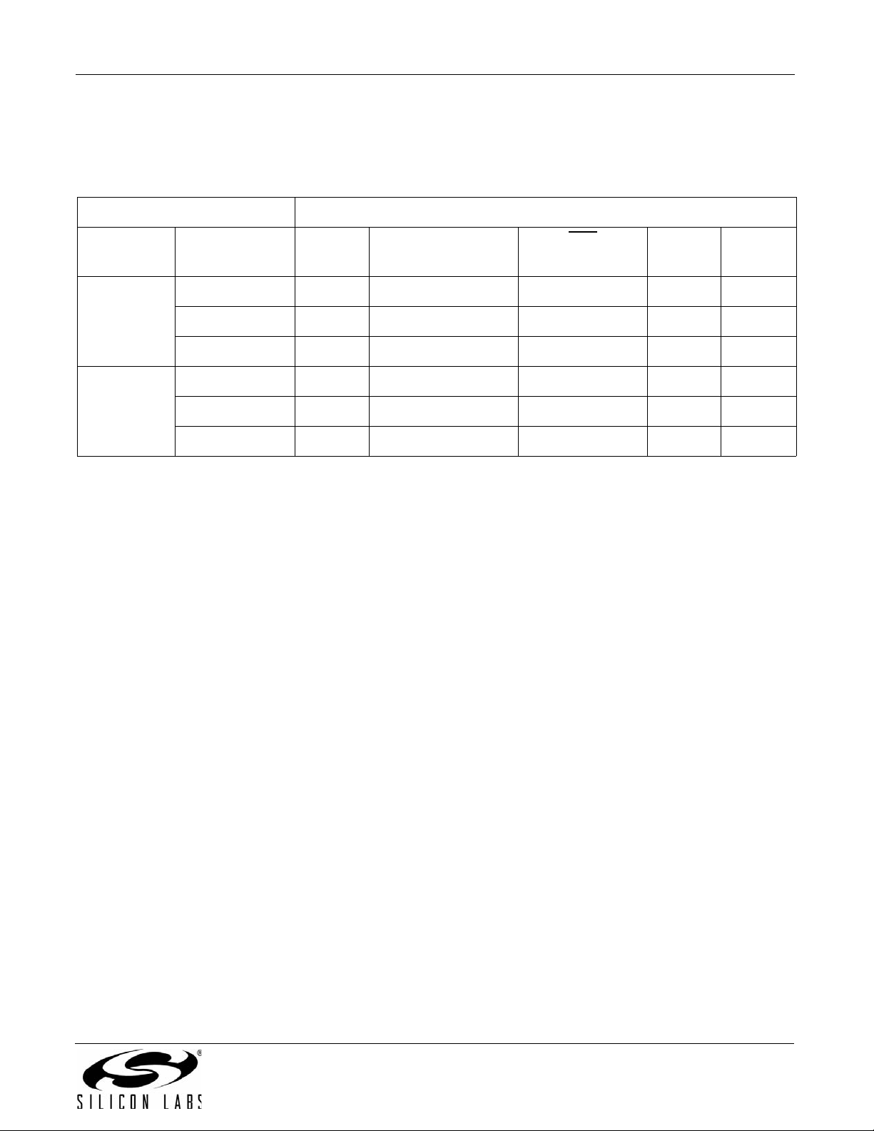
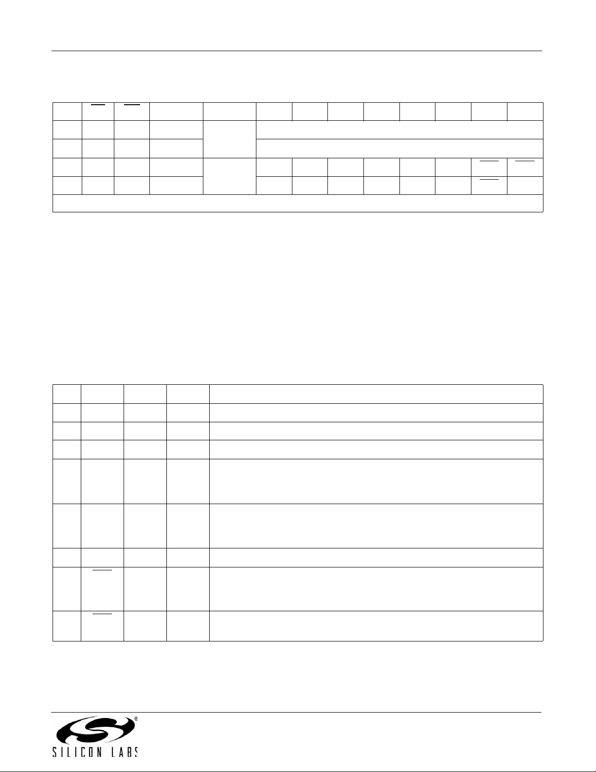
1.1. Selection Guide
Tables 1 through 3 list the modulations, protocols, carriers, tones and interface modes supported by the Si2494/39
and Si2493/57/34/15/04 ISOmodem family. The Si2493 supports all modulations and protocols from Bell 103
through V.92. The Si2457 supports all modulations and protocols from Bell 103 through V.90. The Si2434 supports
all modulations and protocols from Bell 103 through V.34. The Si2415 supports all modulations and protocols from
Bell 103 through V.32bis. The Si2404 supports all modulations and protocols from Bell 103 through V.22bis.
Table 1. Modulations
Modulation Data Rates (bps) Modulation Si2494/93 Si2457 Si2439/34 Si2415 Si2404
V.92* 48k, 40k, 32k, 24k PCM
V.90* 56k, 54.6k, 53.3k, 52k, 50.6k,
49.3k, 48k, 46.6k, 45.3k, 44k,
42.6k, 41.3k, 40k, 38.6k,
37.3k, 36k, 34.6k, 33.3k, 32k,
30.6k, 29.3k, 28k
V.34* 33.6k, 31.2k, 28.8k, 26.4k, 24k,
21.6k, 19.2k, 16.8k, 14.4k, 12k,
9600, 7200, 4800, 2400
V.32bis* 14.4k, 12k, 9600, 7200, 4800 TCM
V.32* 9600
9600, 4800
V.29FC* 9600 QAM
V.23 1200 FSK
V.22bis 2400, 1200 QAM
V.22 1200 DPSK
Bell 212A 1200 DPSK
V.21 300 FSK
Bell 103 300 FSK
*Note: With the Si3018 DAA only.
PCM
TCM
TCM
QAM
*
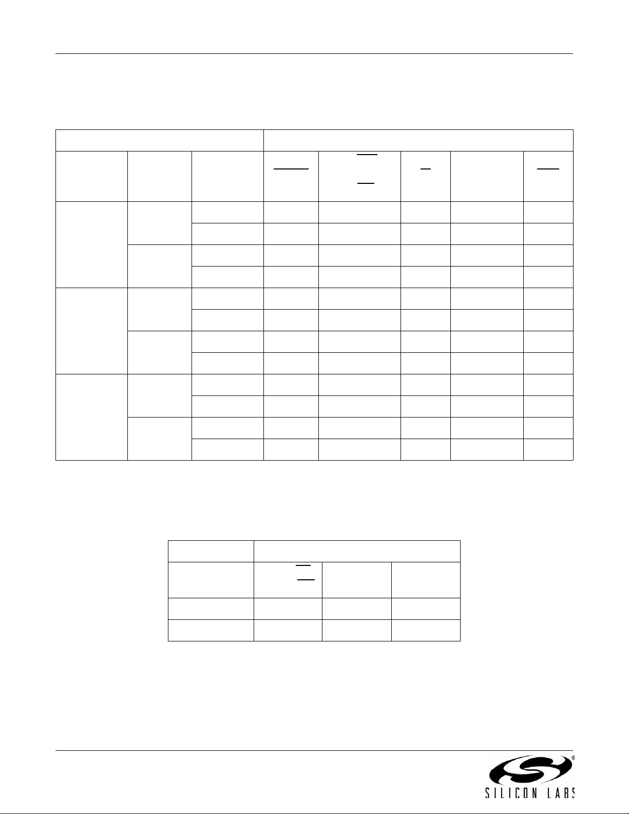
Table 2. Protocols
Protocol*
V.44 Compression
V.42bis Compression
V.42 Error Corre ct ion
MNP5 Compression
MNP2-4 Error Correction
*Note: The Si2494/93/57/39/34/15/04 family allows any supported protocol combined with any modulation.
Function Si2494/93 Si2457 Si2439/34 Si2415 Si2404
Rev. 1.3 9
Page 10

AN93
Table 3. Carriers and Tones
Specification Transmit Carrier
(Hz)
V.92 Variable Variable per ITU-T V.92
V.90 Variable Variable per ITU-T V.90
V.34 Variable Variable per ITU-T V.34
V.32bis 1800 1800 2100 per ITU-T V.32bis
V.32 1800 1800 2100 per ITU-T V.32
V.29 1700 1700 per ITU-T V.29
V.22bis, V.22
Originate/answer
V.21
Originate/answer (M/S)
Bell 212A
Originate/answer
Bell 103
Originate/answer (M/S)
1200
2400
1180/980
1850/1650
1200
2400
1270/1070
2225/2025
Receive Carrier
(Hz)
2400
1200
1850/1650
1180/980
2400
1200
2225/2025
1270/1070
Answer
Tone (Hz)
2100 –43 dBm/–48 dBm
2100 –43 dBm/–48 dBm
2225 –43 dBm/–48 dBm
2225 –43 dBm/–48 dBm
Carrier Detect (Acquire/
Release)
–43 dBm/–48 dBm
–43 dBm/–48 dBm
–43 dBm/–48 dBm
–43 dBm/–48 dBm
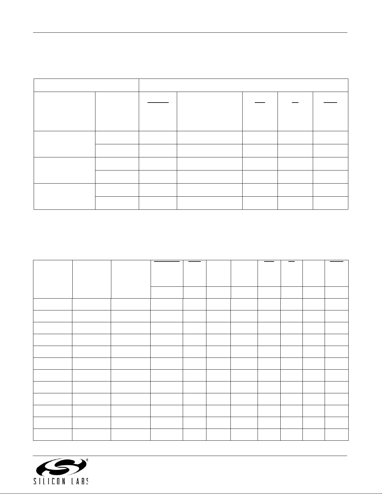
Table 4. ISOmodem Capabilities
Part Numbers Package UART EEPROM SPI Parallel SSI/Voice
Si2493/57/34/15/04
Si2493/57/34/15/04
Si2494/39
Notes:
1. Die Revision D or later
2. The EEPROM interface option is available only when the UART or SPI interface is selected.
1
1
SOIC-16
TSSOP-24
QFN-38
2
10 Rev. 1.3
Page 11

AN93
2. Modem (System-Side) Device
The Si24xx ISOmodem system-side devices contain a controller, a DSP, program memory (ROM), data memory
(RAM), UART, SPI and parallel interfaces, a crystal oscillator, and an isolation capacitor interface. The following
sections describe the reset sequence, the host interface, the isolation interface, low-power mod es, SSI/voice m ode
and the EEPROM interface.
2.1. Resetting the Device
Reset is required after power-on or brownout conditions (the supply dropping to less than the data sheet minimum).
The supply must be stable throughout the minimum required reset time described here and thereafter. A reset is
also required in order to come out of the power down mode.
Some operational choices, including the crystal oscillator frequency used and the command interface used (e.g.
UART vs SPI), is made during the reset time according to pull-down resistors placed on some modem pins. These
pins are modem output lines, but, during reset, the modem places them into a high-impedance mode with weak
internal pull-ups, then reads the user's strapping choices. It is important that the resultant state changes of these
pins during reset are not misinterpreted by the host.
For example the INT output pin of the modem (and perhaps others) can be strapped low with a 10 k resistor to
request SPI operation. If that mode is chosen, the host should take care not to enable this interrupt input before the
modem reset since the INT signal will transition from high to low and back up during reset in this case and can
generate an unexpected interrupt.
If an external clock signal is provided instead of a crystal attached to the modem, it is important that this external
clock signal be stable before the reset ends.
2.1.1. Reset Sequence
After power-on, the modem must be reset by asserting the RESET pin (low) for the required time then waiting a
fixed 300 ms before sending the first A T command. The reset re covery time of 300 ms is also applicable if the reset
is a SW triggered event, such as an ATZ command.
If a 4.9152 MHz crystal or an external 27 MHz clock is used, the reset must be asserted for 5 ms, and a wait of
300 ms duration must happen before an AT command is issued. If a 32 kHz crystal is used, the reset pulse must be
500 ms long and followed by the same 300 ms duration wait as that used for higher frequency clocks.
This is adequate to reset all the on-chip registers. No te tha t 16 µs after the customer-applied reset pulse starts, the
I/O pins will be tri-stated with a weak pull-up, and, 16 µs after the end of this reset pulse, the IO pins will switch to
inputs or outputs as appropriate to the mode indicated by the pull-down strapping. This 16 µs de lay is for newer
revs of the modem parts (those parts that introduce a 32 kHz crystal and SPI operation); older revs exhibit a delay
of only nanoseconds.
The reset sequence described above is appropriate for all user modes of the modem including UART, SPI, and
Parallel bus operation.
A software reset of the modem can also b e pe rfor med by issuing the command ATZ or by setting U-register 6E bit
4 (RST) high using AT commands. After issuing a software or hardware reset, the host must wait for the reset
recovery time before issuing any subsequent AT commands.
There is no non-volatile memory on the ISOmodem other than program ROM. When reset, the ISOmodem reverts
to the original factory default settings. Any set-up or configuration data and software updates must be reloaded
after every reset. This is true whether the reset occurs due to a power-down/power-up cycle, a power-on reset
through a manual reset switch, by writing U6E [4] (RST) = 1, or by executing ATZ.
A suggested reset sequence is as follows:
1. Apply an active-low pulse to the RESET
2. Wait at least the reset r ecovery time.
3. Load firmware updates (if required).
4. Set non-default DAA interface parameters—DCV, ACT, ILIM, OHS2, OHS, RZ, RT, (U67), LIM, (U68).
5. Set non-default cadence values—Busy Tone, Ringback, Ring.
pin; write RST bit or ATZ<CR>.
Rev. 1.3 11
Page 12

AN93
6. Set non-default frequency values—Ring.
7. Set non-default filter parameters.
8. Set non-default S-register values.
The modem is now ready to detect rings, answer another modem, call, or dial out to a remote modem.
Some key default settings for the modem after reset or powerup include the following:
V.92 and fall-backs enabled (Si2494/93)
V.90 and fall-backs enabled (Si2457)
V.34 and fall-backs enabled (Si2439/34)
V.32bis and fall-backs enabled (Si2415)
V.22bis and fall-backs enabled (Si2404)
V.42/42bis enabled
+++ escape sequence enabled
Answer-on-ring is disabled
Speaker off
DTE echo enabled
Verbal result codes enabled
CTS only enabled
FCC (US) DAA and call progress settings
2.1.2. Reset Strapping: General Considerations
The different options available in the Si24xx ISOmodem family are selected by means of 10 k pulldown resistor s
placed at certain pins. During power-on or pin reset, the ISOmodem’s signal pins are read and the option resistors
are taken into account to determine the required configuration. After reset, the ISOmodem assumes the
functionality selected by the corresponding combination of pulldown resistors.
Below is a summary of reset-strap options. Not all options are available on all part number or packages. Refer to
Table 4, “ISOmodem Capabilities,” on page 10 for details.
Host interface: UART, parallel or SPI
Input clock frequency: 32 kHz, 4.9152 MHz or 27 MHz
Autobaud mode or fixed-rate UART communication (when UART interface is selected). Disabling the autobaud
feature at reset sets the rate to 19,200 baud.
EEPROM interface
Three-wire EEPROM or four-wire EEPROM when EEPROM interface is selected
Refer to "2.6. EEPROM Interface (24-Pin TSSOP and 38-Pin QFN Only)" on page 31 for more details on the
various ISOmodem EEPROM options.
The next few sections describe the various reset options that must be selected for each package. In all the tables,
the following conventions apply:
0 means a 10 k pulldown resistor to ground.
1 means the pin is left open. If a pin is left open, the internal pullup resistor is normally sufficient as long as the
pin is not driven externally during reset. If there is noise or special power-sequencing situations, then an
external pullup resistor may be needed.
12 Rev. 1.3
Page 13
AN93
2.1.3. Reset-Strap Options for 16-Pin SOIC Package
The clock frequency and interface on the 16-pin SOIC package are selected according to Table 5 below. The
parallel interface, EEPROM and autobaud options are not available in the 16-pin SOIC package.
Table 5. SOIC-16 Reset-Strap Options
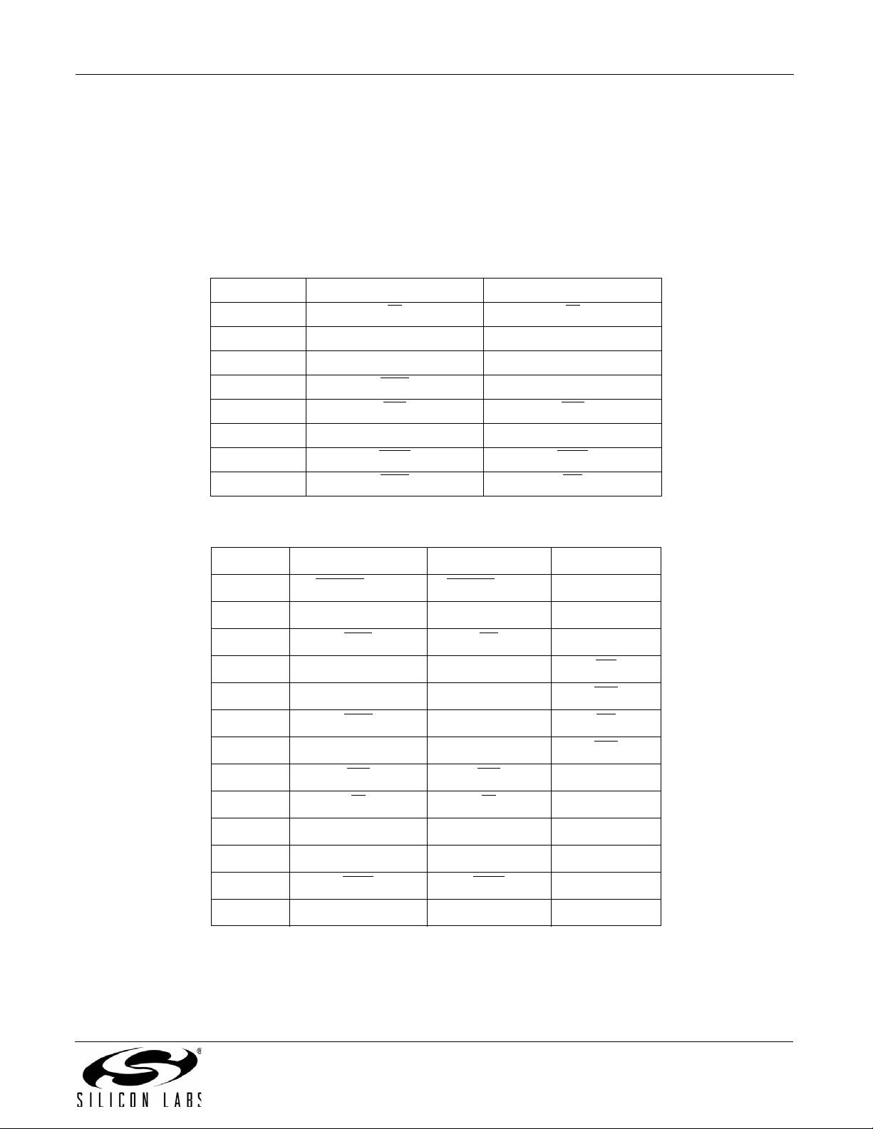
Mode Reset-Strap Pins
Interface Input Clock Pin 3
RI
UART 32 kHz 0 X 1 1 X
4.9152 MHz 1 X 1 1 1
27 MHz 1 X 1 1 0
SPI 32 kHz 1 1 X 0 1
4.9152 MHz 0 1 X 0 X
27 MHz 1 1 X 0 0
2.1.4. Reset-Strap Options for 24-Pin TSSOP Package
The pin-strapping options for the 24-pin TSSOP package are described in the three subsections below, depending
on the interface mode selected.
Pin 5, RXD/MISO Pin 7, CTS
/SCLK Pin 11
INT
Pin 15
DCD
Rev. 1.3 13
Page 14
AN93
2.1.4.1. Reset Strapping Options for TSSOP-24 with UART-Interface
UART-interface options for the 24-pin TSSOP package are shown in Table 6 below.
Table 6. TSSOP-24 UART-Interface Options
Mode Reset-Strap Pins
Input Clock Autobaud
Disabled?
32 kHz No No 1 1 0 1 X
Yes No 1 1 0 0 X
4.9152 MHz No No 1 1 1 1 1
Yes No 1 1 1 0 1
27 MHz No No 1 1 1 1 0
Yes No 1 1 1 0 0
Three-Wire
EEPROM
Interface?
Yes 0 1 0 1 X
Yes 0 1 0 0 X
Yes 0 1 1 1 1
Yes 0 1 1 0 1
Yes 0 1 1 1 0
Yes 0 1 1 0 0
Pin 4
FSYNC
Pin 11, CTS
Pin 15, AOUT
Pin 16, INT
Pin 17
RI
Pin 18
SDI/EESD
Pin 23
DCD
2.1.4.2. Reset Strapping Options for TSSOP-24 with Parallel-Interface
Parallel-interface options for the 24-pin TSSOP package appear in Table 7 below. The EEPROM and autobaud
options are not available when the parallel interface is selected.
Table 7. TSSOP-24 Parallel-Interface Options
Mode Reset-Strap Pins
Input Clock Pin 9, RD
Pin 10, WR
27 MHz 1 0 0
4.9152 MHz 1 1 0
14 Rev. 1.3
Pin 11
SCLK
Pin 15
INT
Page 15
2.1.4.3. Reset Strapping Options for TSSOP with SPI-Inter face
Table 8 lists the SPI-interface options for the 24-pin TSSOP package.
Table 8. TSSOP-24 SPI-Interface Clock-Frequency Options
Mode Reset-Strap Pins
AN93
Input Clock Three-Wire
EEPROM
Interface?
32 kHz No 1 1 0 1 1
Yes 0 1 0 1 1
4.9152 MHz No 1 1 0 0 X
Yes 0 1 0 0 X
27 MHz No 1 1 0 1 0
Yes 0 1 0 1 0
2.1.5. Reset Strapping Options for QFN Parts
2.1.5.1. Reset Strapping Options for QFN Parts with UART Operation
Table 9 lists the reset strapping options for QFN parts with UART operation.
Pin 4
FSYNC
Pin 9, RXD
Pin 11, SCLK
Pin 15, AOUT
Pin 18, SDI/EESD
Pin 16
INT
Pin 17
RI
Table 9. Reset Strapping Options for QFN Parts with UART Operation
Input Clk Auto-Baud
Disable
Three-Wire
EEPROM
Interface
FSYNCH CTS AOUT EECLK INT RI SDI DCD
Pin 23
DCD
Pin 2 Pin 21 Pin 15 Pin 13 Pin 35 Pin 19 Pin 8 Pin 28
32 kHz No No 1 1 1 1 1 1 1 1
Yes 0 1 1 1 1 1 1 1
Yes No 1 1 1 1 1 1 0 1
Yes 0 1 1 1 1 1 0 1
4.9152 MHz No N o 1 1 1 1 1 0 1 X
Yes 0 1 1 1 1 0 1 X
Yes No 1 1 1 1 1 0 0 X
Yes 0 1 1 1 1 0 0 X
27 MHz No No 1 1 1 1 1 1 1 0
Yes 0 1 1 1 1 1 1 0
Yes No 1 1 1 1 1 1 0 0
Yes 0 1 1 1 1 1 0 0
Rev. 1.3 15
Page 16
AN93
2.1.5.2. Reset Strapping Options for QFN Parts with SPI Operation
Table 10 lists the reset strapping options for QFN parts with SPI operation.
Table 10. Reset Strapping Options for QFN parts with SPI Operation
Input Clk Three-Wire
EEPROM
Interface
32 kHz No 1 1 1 0 1 1 1 1
Yes 0 1 1 0 1 1 1 1
4.9152 MHz No 1 1 1 0 0 1 X 1
Yes 0 1 1 0 0 1 X 1
27 MHz No 1 1 1 0 1 1 0 1
Yes 0 1 1 0 1 1 0 1
2.1.5.3. Reset Strapping Options for QFN Parts with Parallel Operation
Table 11 lists the reset strapping options for QFN parts with parallel operation.
FSYNCH AOUT EECLK INT RI SDI DCD MISO
Pin 2 Pin 15 Pin 13 Pin 35 Pin 19 Pin 8 Pin 28 Pin 22
Table 11. Reset Strapping Options for QFN Parts with Parallel Operation
Input Clk CS
AOUT EECLK RD
Pin 21 Pin 15 Pin 13 Pin 22
32 kHz 1 0 1 1
10 1 1
4.9152 MHz 1 0 0 1
10 0 1
27 MHz 0 0 1 1
00 1 1
16 Rev. 1.3
Page 17
AN93
2.2. System Interface
The ISOmodem can be connected to a host processor thro ugh a UAR T, SPI or parallel interface. Connection to the
chip requires low-voltage CMOS signal levels from the host and any other circuitry interfacing directly. The
following sections describe the digital interface options in detail.
2.2.1. Interface Selection
The interface is selected during reset, as described in "2.1. Resetting the Device". Tables 12, 13, and 14 show the
functions of the affected pins for possible interface modes for 16-, 24- and 38-pin packages, respectively.
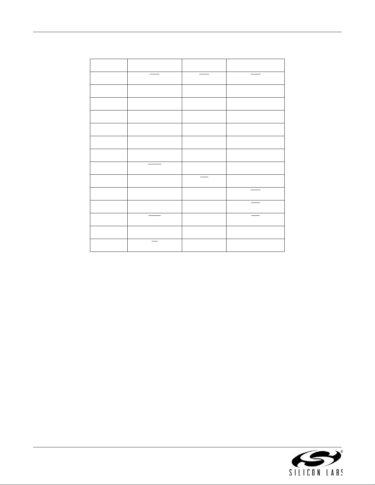
Table 12. Pin Functions vs. Interface Mode (SOIC-16)
Pin # UART Mode SPI Mode
3RI
5 RXD MISO
6 TXD MOSI
7CTS
11 INT
14 ESC ESC
15 DCD
16 RTS SS
RI
SCLK
INT
DCD
Table 13. Pin Functions vs. Interface Mode (TSSOP-24)
Pin # UART Mode SPI Mode Parallel Mode
2 FSYNC
3 CLKOUT (SSI) CLKOUT (SSI) A0
8RTS
9 RXD MISO RD
10 TXD MOSI WR
11 CTS SCLK CS
(SSI) FSYNC (SSI) D6
SS D7
15 AOUT AOUT INT
16 INT INT D0
17 RI
18 SDI (SSI) SDI (SSI) D2
22 ESC ESC D3
23 DCD
24 SDO (SSI) SDO (SSI) D5
Rev. 1.3 17
RI D1
DCD D4
Page 18
AN93
Table 14. Pin Functions vs. Interface Mode (QFN-38)
Pin # UART Mode SPI Mode Parallel Mode
35 INT
34 GPIO18 GPIO18 D0
33 GPIO17 GPIO17 D1
32 GPIO16 GPIO16 D2
31 GPIO23 GPIO23 D3
30 GPIO24 GPIO24 D4
29 ESC D5
28 DCD
24 RTS SS
23 TXD MOSI WR
22 RXD MISO RD
21 CTS SCLK CS
20 GPIO11 G PIO11 A0
19 RI
INT INT
D6
D7
18 Rev. 1.3
Page 19
2.2.2. Interface Signal Description
The following tables describe each set of UART, parallel and SPI interface signals:
Table 15. UART-Interface Signals
Signal Direction Description
TXD Input Data input from host TXD pin
RXD Output Data output to host RXD pin
AN93
RTS
CTS
Input Active-low request-to-send input for flow control
Output Clear to send: Si249 3 is ready to receive data on the TXD pin (active low)
Table 16. SPI-Interface Signals
Signal Direction Description
SCLK Input Serial data clock
MISO Output Serial data output
MOSI Input Ser ia l data input
SS
INT
Input Chip select (active low)
Output Interrupt (active low)
Table 17. Parallel-Interface Signals
Signal Direction Description
A0 Input Register selection (address inpu t)
CS
RD
WR
D[7:0] Bidirectional Parallel data bus
INT
Input Chip select (active low)
Input Read enable (active low)
Input Write enable (active low)
Output Interrupt (active low)
2.2.3. UART Interface Operation
The UART interface allows the host processor to communicate with the modem controller through a UART driver.
In this mode, the modem is analogous to an external “box” modem. The interface pins are 5 V tolerant and
communicate with TTL-compatible, low-voltage CMOS levels. RS232 interface chips, such as those used on the
modem evaluation board, can be used to make the UART interface directly compatible with a PC or terminal serial
port.
2.2.3.1. UART Options
The DTE rate is set by the autobaud feature after reset. When autobaud is disabled, the UART is configured to
19.2 kbps, 8-bit data, no parity and 1 stop bit on reset. The UART data rate is programmable from 300 bps to
307.2 kbps with the AT\Tn command (see Table 42, “Extended AT\ Command Set,” on page 81). After the AT\Tn
command is issued, the ISOmodem echoes the result code at the old DTE rate. After the result code is sent, all
subsequent communication is at the new DTE rate.
The DTE baud clock is within the modem crystal tolerance (typically ±50 ppm), except for DTE rates that are
uneven multiples of the modem clock. All DTE rates are within the +1%/–2.5% required by the V.14 specification.
Table 18 shows the ideal DTE rate, the actual DTE rate, and the approximate error.
Rev. 1.3 19
Page 20
AN93
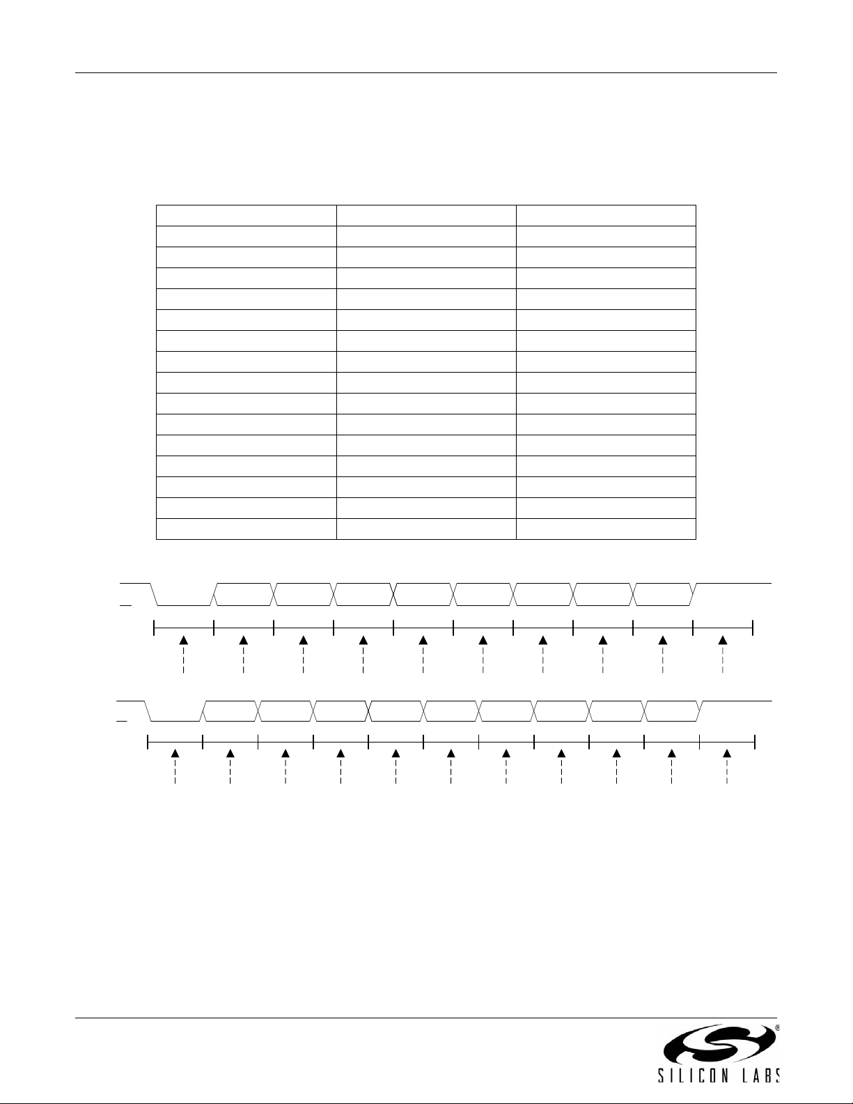
D1D0 D2 D3 D4 D5 D6 D7
START
BIT
MARK
STOP
BIT
BIT TIMES
BIT SAMPLING
SPACE
D1D0 D2 D3 D4 D5 D6 D7
START
BIT
MARK
STOP
BIT
BIT TIMES
BIT SAMPLING
SPACE
D8
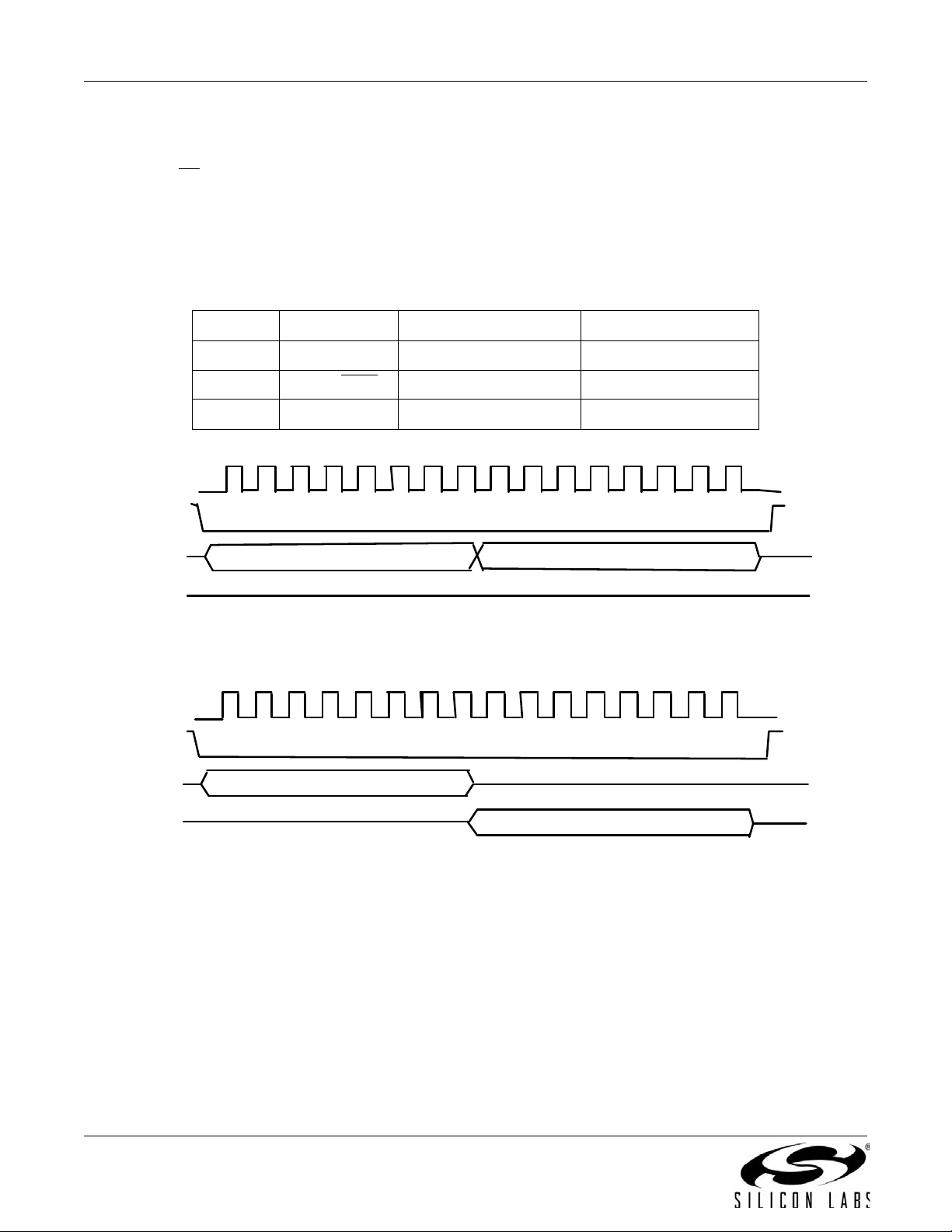
The UART interface synchronizes on the start bits of incoming characters and samples the data bit field and stop
bits. The interface is designed to accommodate character lengths of 8, 9, 10, and 11 bits giving data fields of 6, 7,
8, or 9 bits. Data width can be set to 6, 7, or 8 bits with the AT\Bn command. Parity can be set to odd, even, mark,
or space by the AT\Pn command in conjunction with AT\B2 or AT\B5. Other AT\Bn settings have no parity.
Table 18. DTE Rates
Ideal DTE Rate (bps) Actual DTE Rate (bps) Approximate Error(%)
300 300
600 600
1200 1200
2400 2400
7200 7202 0.01
9600 9600
12000 12003 0.02
14400 14400
19200 19200
38400 38400
57600 57488 0.2
115200 115651 0.4
230400 228613 0.8
245760 245760
307200 307200
Figure 2. Asychronous UART Serial Interface Timing Diagram
2.2.3.2. Autobaud
When set in UART interface mode, the ISOmodem in cludes an automatic baud rate detection feature that allows
the host to start transmitting data at any standard DT E r ate from 300 bps to 307.2 kbps. This feature is enabled by
default. When autobaud is enabled, it continually adjusts the baud rate, and the ISOmodem always echoes result
codes at the same baud rate as the most recently received character from the host. Autobaud can be turned off
using AT commands \T0 through \T15, and \T17. Host software should disable autobaud operation once the DTE
rate has been established. This prevents transients on TXD to cause inadvertent baud rate changes.
Autobaud is off when dialing, answering, and in data mode. When autobaud mode is off, the baud rate is set to the
most recently-active baud rate prior to entering one of these states. When autobaud mode is on, autoparity is
performed when either “at” or “AT” is detected. Autoparity detects the formats listed in Table 19.
20 Rev. 1.3
Page 21

AN93
:
Table 19. Serial Formats Detected in Autobaud Mode
Symbol Data bits Parity Stop bits
7N1 7 None (mark) 1
7N2 7 None (mark) 2
7S1 7 None (space) 1
7O1 7 Odd 1
7E1 7 Even 1
8N1 8 None (mark) 1
8E1 8 Even 1
8O1 8 Odd 1
9N1 9 None (mark) 1
Note: For 7N1, the modem is programmed to 7 data bits, mark parity and one stop bit. This may be changed with the AT\P and
AT\B commands. In autobaud mode, 7N1 is properly interpreted and echoed, but the AT\P and AT\B commands must be
sent prior to dialing in order to lock the parity and format to 7N1. Otherwise, the ISOmodem lo cks to 7 bits, mark parity
and two stop bits (7N2).
2.2.3.3. Flow Control
The ISOmodem supports flow control through RTS
from the terminal (DTE) to the modem (DCE) indicating data may be sent from the modem to the terminal. CTS
(clear-to-send) is a control signal from the modem (DCE) to the terminal (DTE) indicating data may be se nt from
the terminal to the modem for transmission to the remote modem. This arrangement is typically referred to as
hardware flow control. There is a 14-character FIFO and a 1024 character elastic transmit buffer (see Figure 3).
goes inactive (high) when the 1024 character buffer reaches 796 characters, then reasserts (low) when the
CTS
buffer falls below 128 characters. There is no provision to compensate for FIFO overflow. Data received on TXD
when the FIFO is full are lost.
XON/XOFF is a software flow control method in which the modem and terminal control the data flow by sending
XON characters (^Q/0x11) and XOFF characters (^S/0x13). XON/XOFF flow control is enabled on the ISOmodem
with AT\Q4.
does not de-assert during a retrain (see Table 45: S9, Carrier presence timer and S10, Carrier loss timer).
DCD
always deasserts during initial training, retrain, and at disconnect regardless of the \Qn setting. For \Q0 CTS,
CTS
flow control is disabled; CTS
automatic retrains. The host can force a retrain by escaping to the command mode and sending ATO1 or ATO2.
The DCD
pin can be programmed to monitor the bits in r egister U7 0 listed in Table 20. The RI, PPD, OCD, CID, and RST bits
are sticky, and the AT:I command reads and clears these signals and deactivates the INT
and RI pins can be used as hardware monitors of the car rier detect an d ring sig nals. Add itionally, the INT
is inactive during data transfer. The modem remains in the data mode during normal
/CTS and XON/XOFF. RTS (request-to-send) is a control signal
pin if INT is enabled.
Rev. 1.3 21
Page 22
AN93
796 Characters
128 Characters
1024 Character Elastic Tx Buffer
SRAM
CTS Deasserts
CTS A sserts
Transmit
14-Character
Hardw are
Buffer
Tx D ata
CTS
796 Characters
128 Characters
1024 Character Elastic Rx Buffer
SRAM
Receive
12-Character
Hardw are
Buffer
Rx data
RTS
RXF bit
REM bit
Parallel
Mode
Table 20. Register U70 Signals INT
Signal U70 Bit Function
DCD 0 Data Carrier Detect—active high (inverse of DCD
RI 1 Ring Indicator—active high (inverse of RI
PPD 2 Parallel Phone Detect
OCD 3 Overcurrent Detect
CID 4 Caller ID Preamble Detect
Can Monitor
pin)
pin)
Figure 3. Transmit Data Buffers
22 Rev. 1.3
Figure 4. Receive Data Buffers
Page 23
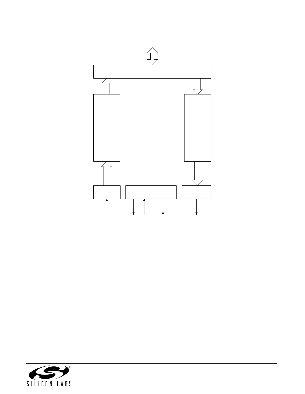
A block diagram of the UART in the serial interface mode is shown in Figure 5.
11 Bits
to Data Bus
CONTROL
RX Shift
Register
TX Shift
Register
TX FIFO
MUX
TXD
(10)
CTS
(11)
RTS
(8)
RXD
(9)
INT
(16)
RX FIFO
.
AN93
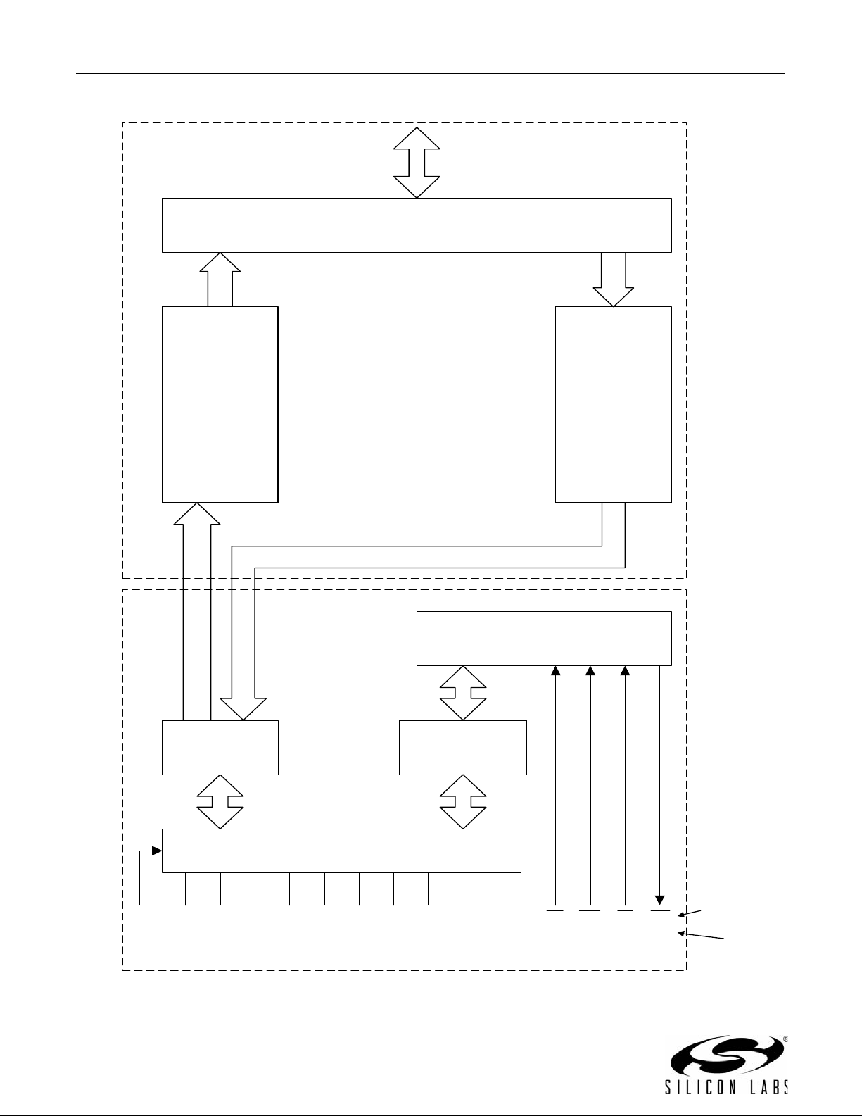
2.2.4. Parallel and SPI Interface Operation
Refer to "2.1. Resetting the Device" on page 11 for interface selection. The parallel interface has an 8-bit data bus
Figure 5. UART Serial Interface
and a single address bit. The SPI likewise operates with 8-bit data transfers, using a single address bit. When the
parallel or SPI interface mode is selected, the modem must be configured fo r a DTE interface or 8N1 only. The host
processor must calculate parity for the MSB. The modem sends bits as received by the host and does not calculate
parity. Refer to "Appendix C—Parallel/SPI Interface Software Implementation" on page 290 for detailed parallel or
SPI interface application information.
The parallel or SPI interface uses the FI FOs t o bu ffer data in the sam e way as in UART mode, with the addit ion o f
Hardware Interface Registers 0 (HIR0) and Hardware Interface Register 1 (HIR1). The Hardware Interface
Registers were formerly called Parallel Interface Registers (PIR0 and PIR1) in older products, because those
products would support only a parallel interface. Flow contr ol must be imple mented by monitor ing REM a nd TXE in
HIR1. There is no protection against FIFO overflow. Data transmitted when the transmit FIFO is full are lost.
Figure 6 shows the interaction of the transmit and receive FIFOs with the Hardware (Parallel) Interface Registers in
the case of a parallel interface. The arrangement is sim ilar wh en the SPI inter face is selecte d. Table 21 on page 25
shows a bit map of HIR0 and HIR1.
UART oriented control lines, such as RTS and CTS, are not used in Parallel and SPI Interface mode. They are
replaced by bits in the HIR1 register.
SPI and parallel operation only support s 8- bit dat a word s. The longer wor ds that are implied by the \B5 (8P1) & \B6
8X1 commands are not allowed. These commands should not be used.
Rev. 1.3 23
Page 24
AN93
11 Bits
to Da ta Bus
CONTROL
Para lle l I/F
Register 1
MUX
Para lle l I/F
Register 0
A
0
(3)
D
0
(16)
D
1
(17)
D
2
(18)
D
3
(22)
D
4
(23)
D
5
(24)
D
6
(4)
D
7
(8)
RD
(9)WR(10)CS(11)
INT
(15)
MUX
Parallel Interface Unique
Shared-Serial/Parallel
Parallel mode pin function
Parallel mode pin number
TX FIFO
14 Characters
RX FIFO
12 Characters
24 Rev. 1.3
Figure 6. Parallel Interface
Page 25
AN93
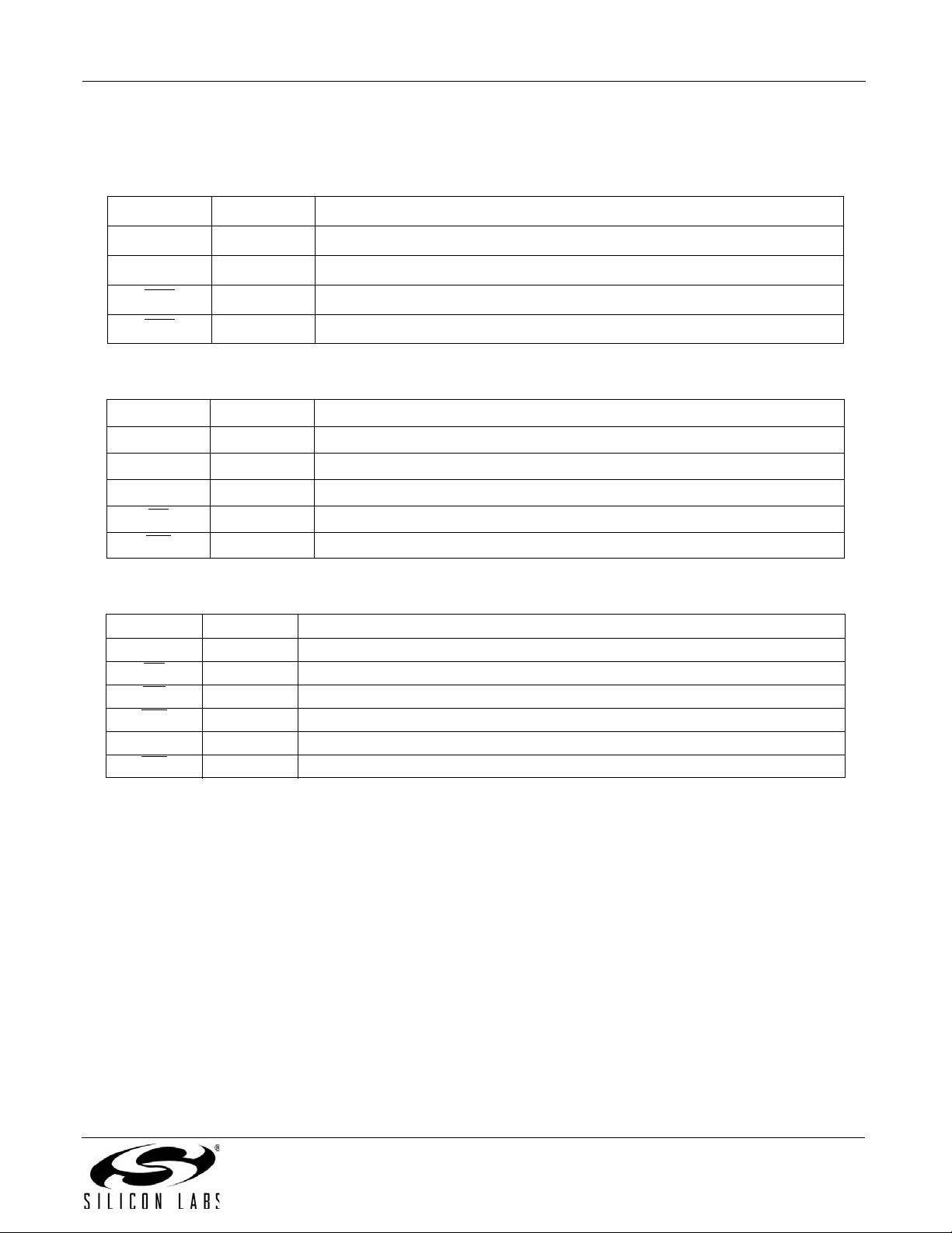
Table 21. Hardware Interface Register Bit Map
A0 RD WR Action Register D7 D6 D5 D4 D3 D2 D1 D0
0 0 1 Read HIR0 Modem data or command from receive FIFO
0 1 0 Write Modem data or command to transmit FIFO
1 0 1 Read HIR1 RXF TXE REM INTM INT ESC RTS
1 1 0 Write RXF TXE *Note INTM *Note ESC RTS n/a
*Note: RE M and INT are read-only bits.
2.2.4.1. Hardware Interface Register 0
Hardware Interface Register 0 (HIR0) is the eight-bit wide read/write location where modem data and commands
are exchanged with the host. Writing a byte to the HIR0 adds that byte to the modem’s transmit FIFO (AT
command buffer in command mode or data transmission in data mode). If data are available (modem data in data
mode or command responses, such as OK, in command mode), reading from the HIR0 fetches data from the
modem’s receive FIFO. The maximum burst data rate is approximately 350 kbps (45 kBps).
2.2.4.2. Hardware Interface Register 1
Hardware Interface Register 1 (HIR 1) contains various s tatus and control flags for use by the host to perform data
flow control, to escape to command mode and to query various in terrup t co ndition s. The HIR1 bit ma p is de scr ibe d
in Table 22. This register is reset to 0x63.
CTS
Table 22. Hardware Interface Register 1
Bit Name R/W Reset Function
7RXFR/W 0Receive FIF O Almost Full
6TXER/W 1Transmit FIFO Almost Empty
5REM R 1Receive FIFO Empty
4INTMR/W 0Interrupt Mask
0 = INT pin triggered on risin g ed ge of RXF or TXE only
1 = INT pin triggered on rising edge of RXF, TXE or INT (bit 3 below)
3INT R 0Interrupt
0 = No interrupt
1 = Interrupt triggered
2 ESC R/W 0 Escape
1RTS
0CTS
Bit 7 (RXF) is a read/write bit that gives the status of the 12-byte deep receive FIFO. If RXF = 0, the receive FIFO
contains less than 10 bytes. If RXF = 1, the receive FIFO contains more than 9 bytes and is full or almost full.
Writing RXF = 0 clears the interrupt.
R/W 1 Request-to-Send (active low) — Deprecated — for flow control, use the
TXE and REM bits for polling- or interrupt-based communication.
This bit must be written to zero.
R1Clear-to-Send (active low) — Deprecated — for flow control, use the TXE
and REM bits for polling- or interrupt-based communication.
Rev. 1.3 25
Page 26
AN93
Bit 6 (TXE) is a read/write bit that gives the status of the 14-byte deep transmit FIFO. If TXE = 0, the transmit FIFO
contains three or more bytes. If TXE = 1, the transmit FIFO contains two or fewer bytes. Writing TXE = 0 clears the
interrupt but does not change the state of TXE.
Bit 5 (REM) is a read-only bit that indicates when the receive FIFO is empty. If REM = 0, the receive FIFO contains
valid data. If REM = 1, the r eceive FIFO is empty. The timer interrupt set by U6F ensures that the receive FIFO
contents 9 bytes are serviced properly.
Bit 4 (INTM) is a read/write bit that controls whether or not INT (bit 3) triggers the INT
Bit 3 (INT) is a read-only bit that reports Interrupt status. If INT = 0, no interrupt has occurred. If INT = 1, an
interrupt due to CID, OCD, PPD, RI, or DCD (U70 bits 4 , 3, 2, 1, 0, respectively) has occurr ed. This bit is reset by :I.
Bit 2 (ESC) is a read/write bit that is functionally equivalent to the ESC pin in the serial mode. The operation of this
bit, like the ESC pin, is enabled by setting U70 [15] (HES) = 1.
The use of bits 1 and 0 (RTS
of bits 6 and 5 (TXE and REM) is recommended for polling- and interrupt-based communication.
2.2.4.3. Parallel Interface Operation
When the device is powered up for parallel interface, the pins include eight data lines (D7–D0), a single address
(A0), a read strobe (RD
the parallel-interface signals:
and CTS) has been deprecated for both parallel and SPI interfaces. Instead, the use
), a write strobe (WR), an interrupt line (INT), and chip select (CS). Table 23 summarizes
Table 23. Parallel Interface Signals
pin.
Signal Function Direction
CS
A0 Register address Input
RD
WR
D[7:0] Data bus Bidirectional
INT
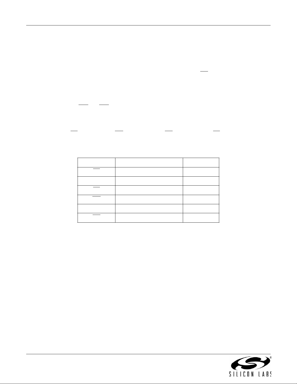
Refer to the device data sheet for timing characteristics. Address pin A0 allows the host processor to choose
between the two interface register s, HIR0 and HIR1. The timing diagrams below show typical parallel-interface
operation. Refer to the respective product data sheets for timing specifications.
Chip Select (active low) Input
Read strobe (active low) Input
Write strobe (active low) Input
Interrupt (active low) Output
26 Rev. 1.3
Page 27
Figure 7. Parallel Interface Read Timing
AN93
Figure 8. Parallel Interface Write Timing
Rev. 1.3 27
Page 28
AN93
Z
Z
Z
Z
2.2.4.4. SPI Interface Operation
SPI interface operation is supported in the Si2493/57/34/15/04 Re vision D o r later and the Si24 94/39 Revision A or
later. When the device is powered up for SPI interface, the modem becomes an SPI slave, and the pins are
configured to SS
modem) and SCLK (serial data clock input). The HIR0 and HIR1 registers described above are also available in
SPI mode. Each SPI operation consists of a control-and-address byte and a data byte. The bit definitions of the
control-and-address byte are shown in Table 24. The timing diagrams that follow show SPI read and write
waveforms. Refer to the device data sheet for timing characteristics.
(chip select input, active low), MOSI (serial data input to modem), MISO (serial data output from
Table 24. SPI Control-and-Address Bit Definitions
Bit Function Meaning when High Meaning when Low
7 Address Access HIR1 Access HIR0
SCK
NSS
MISO
MOSI
SCK
NSS
MISO
MOSI
6 Read/Write
5:0 Reserved Not allowed Must be all zeroes
Ad dre ss /C ont r ol
Read register Write register
Data
SPI2‐ByteWriteProtocol
Address/Control
Data
Hi‐
Hi‐
Hi‐
Hi‐
SPI2‐ByteRe ad Pr oto col
Figure 9. SPI Read and Write Timing Diagrams
2.2.4.5. Interface Communication Modes
Data flow control is implemented in the SPI and parallel interfaces differently from UART mode. When parallel or
SPI mode is selected, data communication may be driven by interrupts or by polling. Refer to "Appendix C—
Parallel/SPI Interface Software Implementation" on page 290 for implementation details for both methods. The
parallel and SPI interfaces have four sources of interrupts and only one inter rupt pin. The four interrupts are:
1. RXF Interrupt: receive FIFO almo st full
2. TXE Interrupt: transmit FIFO almost empty
3. Timer Interrupt: receive FIFO not empty
4. U70 Interrupt: various conditions, such as ringing, parallel phone pickup, etc. as defined in register U70
The source of the interrupt can be determined by reading HIR1.
28 Rev. 1.3
Page 29

AN93
2.3. Isolation Capacitor Interface
The isolation capacitor is a proprietary high-speed interface connecting the modem chip and the DAA chip through
a high-voltage isolation barrier provided by two capacitors. It serves three purposes. First, it transfers control
signals and transmit data from the modem chip to the DAA chip. Second, it transfers receive and status data from
the DAA chip to the modem chip. Finally , it provides po wer from th e mo dem chip to the DAA chip while the modem
is in the on-hook condition. The signaling on this interface is intended for communication between the modem and
the DAA chips and cannot be used for any other purpo se. It is import ant to kee p the length of the ISOcap™ p ath as
short and direct as possible. The layout guidelines for the pins and components associated with this interface are
described in "4.4. Layout Guidelines" on page 49 and must be carefully followed to ensure proper operation and
avoid unwanted emissions.
2.4. Low-Power Modes
2.4.1. Power-Down Mode
The Power-Down mode is a lower power state than sleep mode. It is entered immediately upon writing
U65 [13] (PDN) = 1. Once in the Power-Down mode, the modem requires a hardware reset via the RESET
become active again.
2.4.2. Wake-on-Ring Mode
The ISOmodem can be set to enter a low-power wake-on-ring mode when not connected. Wake-on-ring mode is
entered using the command AT&Z. The ISOmodem returns to the active mode when one of the following happens:
There is a 1 to 0 transition on TXD in the UART mode
There is a 1 to 0 transition on CS in the parallel mode
There is a 1 to 0 transition on SSS in the SPI mode
An incoming ring is detected
A parallel telephone is picked up
Line polarity reversal
2.4.3. Sleep Mode
The ISOmodem can be set to enter a low-power sleep mode when not connected and after a period of inactivity
determined by the S24 register.
The ISOmodem enters the sleep mode S24 seconds after the last DTE activity, after the transmit FIFO is empty,
and after the last data are received from the remote modem. The ISOmodem returns to the active mode when one
of the following happens:
There is a 1 to 0 transition on TXD in the UART mode
There is a 1 to 0 transition on CS in the parallel mode
There is a 1 to 0 transition on SSS in the SPI mode
An incoming ring is detected
A parallel telephone is picked up
Line polarity reversal
The delay range for S24 is 1 to 255 seconds. The default se tting of S24 = 0 disables the sleep timer and keeps the
modem in the normal power mode regardless of activity level.
pin to
Rev. 1.3 29
Page 30
AN93
Si24xx Modem
Si3000 Voice Codec
Si30xx
DAA
Handset
HOST
AT commands
Responses
2- wire
SDISDO
FSYNC MCLK
CLKOUT
SDI
SDO
FSYNC
TDMA Interface
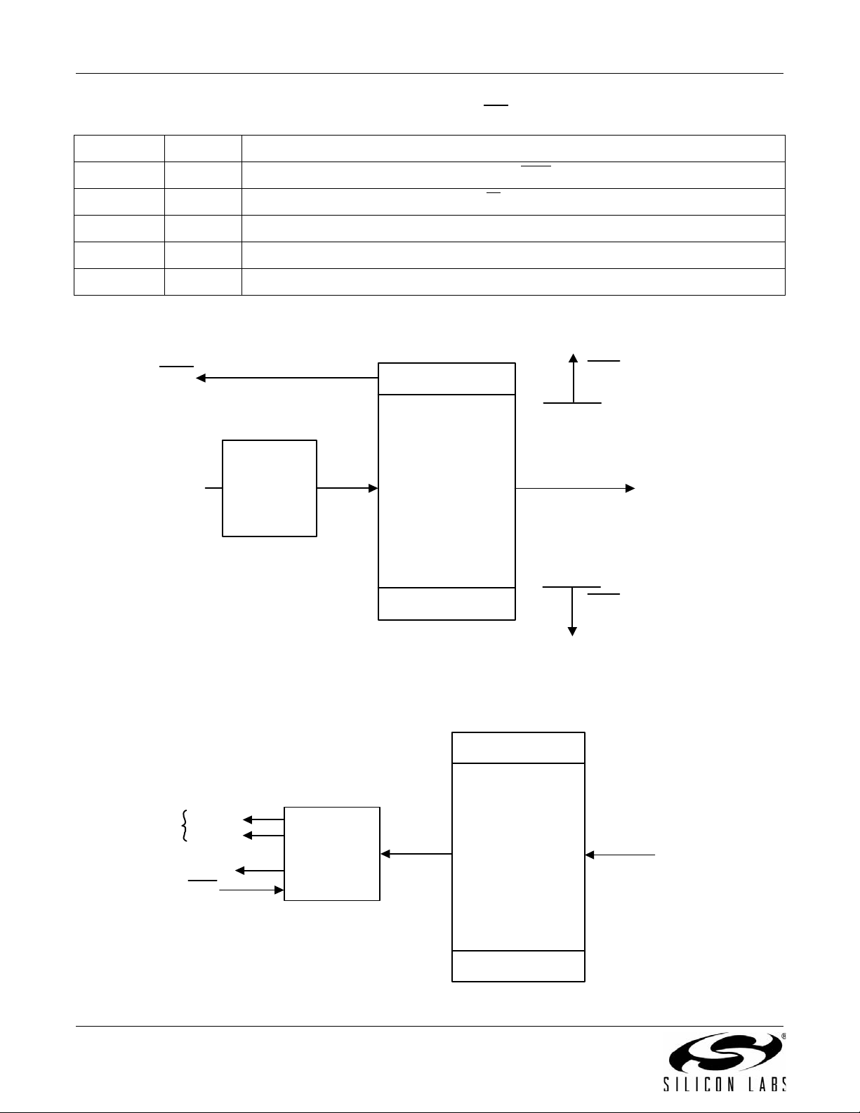
2.5. SSI/Voice Mode (24-Pin TSSOP and 38-Pin QFN Only)
Voice mode is supported in the Si2439 and the Si2494. Table 25 lists the pin connections for the ISOmodem SSI
interface. This interface enables Voice Mode operation. See "7. Handset, TAM, and Speakerphone Operation" on
page 173 for additional information.
Table 25. SSI Interface Pin Connection
Signal Pin Number
(TSSOP-24)
CLKOUT 3 3
FSYNC
SDI 18 8
SDO 24 9
RESET
The Si3000 is used in conjunction with the ISOmodem to transmit and receive 16-bit voice samples to and from
telephone lines as shown in Figure 10.
42
12 16
Pin Number
(QFN-38)
Figure 10. Voice Mode Block Diagram
30 Rev. 1.3
Page 31

AN93
2.6. EEPROM Interface (24-Pin TSSOP and 38-Pin QFN Only)
The 24-pin TSSOP and 38-pin QFN packages feature an optional three-wire interface (EESD, EECS and EECLK)
that may be directly connected to SPI EEPROMs. An EEPROM may contain custom default settings, firmware
upgrades, and/or user-defined AT command macros for use in custom AT commands or country codes. Firmware
upgrades may also be automatically loaded into the ISOmodem using the BOOT format.
2.6.1. Supported EEPROM Types
The EEPROM must support SPI mode 3 with a 16-bit (8–64 kbit range) address. The EEPROM must be between
8192 and 65536 bits in size and support the commands given in Table 26. The EEPROM must also support 16-bit
addressing regardless of size, allow a clock frequency of at least 1 MHz, assert its output on falling edges of
EECLK and latch input data on rising edges of EECLK. All data are sent to and from the EEPROM with the LSB
first. Required EEPROM command format and signal timing are shown in Tables 26 to 28. A typical EEPROMaccess timing diagram is shown on Figure 11. Such EEPROMs are available from several different manufacturers,
for example:
Microchip: 25LC080..25LC640
Atmel: AT25080..AT25640
Table 26. EEPROM Commands
Instruction Name Instruction Format Description
READ 0000 0011 Read data from memory at address
WRITE 0000 0010 Write data to memory array beginning at address
WRDI 0000 0100 Clear write enable bit (disable write operation)
RDSR 0000 0101 Read status register
WRSR 0000 0001 Write status register
WREN 0000 0110 Set write enable bit (enable write operations)
Table 27. EEPROM Status Register (Any Other Bits are Unused)
76543210
——————WELWIP
WEL = write enable latch
WIP = write in progress
Table 28. EEPROM Timing
Parameter Symbol Min. Typ. Max. Unit
EECLK period
EESD input setup time
ECLK 1.0 — — µs
EISU 100 — — ns
EESD input hold time
EESD output setup time*
EESD output hold time*
asserted to EECLK positive edge
EECS
EIH 100 — — ns
EOSU 500 — — ns
EOH 500 — — ns
ECSS 500 — — ns
Rev. 1.3 31
Page 32

AN93
ECLK
LSB
MSB
EISU
EOSU
EIH
EDH
ECSH
ECSW
EOZ
ECSS
EEPROM Data Format
EESD
EECS
8-bit instruction 16-bit address 8-bit data
EOH
Table 28. EEPROM Timing
Parameter Symbol Min. Typ. Max. Unit
EESD tristated before last falling EECLK edge during read
cycle. Last positive half of EECLK cycle is extended to provide
both 500 ns minimum EOH and 100 ns EESD before EECLK
falling edge.
EOZ 100 — — ns
disable time between accesses
EECS
asserted after final EECLK edge
EECS
*Note: EESD output at negative EECLK edge
ECSW 500 — — ns
ECSH 1 — — µs
Figure 11. EEPROM Serial I/O Timing
32 Rev. 1.3
Page 33

AN93
HOST
SPIEEPROM
SI/SO CS SCLK
MODEM
EESD EECS SCLK
Si3018/10
TELEPHONELINE
2.6.2. Three-Wire SPI Interface to EEPROM
To enable the 3-wire SPI interface to EEPROM on the 24-pin TSSOP package, appropriate pins must be reset
strapped according to Table 6 on page 14, or Table 8 on page 15, depending on the interface selected. The
EEPROM option is not available on the 24-pin TSSOP package if the parallel host interface is selected.
Figure 12 shows the connection diagram for the 3-wire SPI interface to EEPROM. A four-wire EEPROM (with
separate serial input and output data wires) may also be used with the input and output pins connected to EESD, if
its SO output is tristated on the last falling edge of EECLK during a read cycle.
Figure 12. Three-Wire EEPROM Connection Diagram
2.6.3. Detailed EEPROM Examples
Upon powerup, if the option is selected, the ISOmodem attempts to detect an EEPROM. The modem looks for a
carriage return in the first 10 memory locations. If none is found, the modem assumes the EEPROM is not
programmed and stops reading it. If a programmed EEPROM is detected, customer defaults that are programmed
into the EEPROM between the optional heading "BOOT " and the "<CR><CR>" delimiter are executed immediately,
and AT command macros are loaded into the ISOmodem RAM. The memory that may be allocated to the
<commands> portion of the EEPROM is limited to 1000 bytes. Three <CR> must be the last three entries in the
EEPROM.
EEPROM Data are stored and read in hexadecimal ASCII format in eight address blocks beginning at a specified
hexadecimal address. For example, the AT:M0000,y0,y1,y2,y3,y4,y5,y6,y7 command writes the hexadecimal
values y0…y7 at addresses from 0 to 7, respectively. The AT:E0000 command reads the hexadecimal values
y0…y7 from addresses 0 to 7, respectively.
The following sections give specific examples of EEPROM usage for command macros, firmware upgrades, boot
commands, etc.
2.6.4. Boot Commands (Custom Defaults)
Commands to be executed upon boot-up are stored between the heading BOOT and the first <CR><CR> delimiter.
The boot command has the following format:
BOOT<CR>
<commands><CR>
<commands><CR>
<CR>
Rev. 1.3 33
Page 34

AN93
The commands end with a <CR>, which, in co mbination with the final<CR>, provides the <CR><CR> delimiter.
Boot commands must be the first entry in the EEPROM and are used to set the modem up with custom defaults,
such as settings for specific countries, auto answer, or other special settings upon power up or after a hardware or
software reset.
This saves the host processor from re loading sp ecial c onfiguration strings at power up or after a reset, and allows
the modem to be customized by programming the EEPROM or by substituting preprogrammed EEPROMs. If the
BOOT command is the final entry in the EEPROM, it must end with an additional <CR> to provide the
<CR><CR><CR> delimiter indicating the end of the EEPROM.
2.6.5. AT Command Macros (Customized AT Commands)
Macros allow the creation of single custom AT commands that execute combinations of default AT commands
including special register configurations. AT command macros have the following format:
<command name><CR>
<commands><CR>
<commands><CR>
<CR>
Each AT Command Macro ends with a <CR><CR>. The final entry in the EEPROM ends with an additional <CR>
to provide the <CR><CR><CR> delimiter indicating the end of the EEPROM. AT command macros can have a
name consisting of any string of characters but must be the only command on a line.
2.6.6. Firmware Upgrades
Firmware upgrades (“patches”) are typically executed upon boot-up and stored between the heading, BOOT, and
the first <CR><CR> delimiter. A firmware upgrade has the format: BOOT<firmware upgrade><CR>. The firmware
upgrade ends with a <CR>, which, in combination with the final<CR>, provides the <CR><CR> delimiter, which
marks the end of the EEPROM contents. A firmware upgrade can also be stored as an AT command macro in a
system where using the firmware upgrade is optional. The following are examples of boot commands, AT
command macros, and automatically-loaded firmware upgrades.
2.6.6.1. Boot Command Example
On power-up or reset, it is desired to set the UART rate to 115.2 kbps and limit the ISOmodem to V.34 and lower
operation.
The AT commands required to do this manually are:
AT\T12<CR>
AT&H2<CR>
To implement this as a boot command, the commands are:
BOOT<CR>
AT\T12<CR>
AT&H2<CR>
<CR>
This must be written to the EEPROM as ASCII hexadecimal in eight address blocks. The actual AT commands to
store this boot command in the EEPROM starting at address 0 are:
AT:M0000,42,4F,4F,54,0D,41,54,5C
AT:M0008,54,31,32,0D,41,54,26,48
AT:M0010,32,0D,0D,00,00,00
The value 0x41 corresponds to the displa y character A, 0x 54 to T, 0x42 to B, 0x4F to O etc., and the value 0x0D,
for carriage return corresponds to the decimal value, 13, stored in S-register 3 (S3). Table 30 shows the
relationship between the decimal values, hexadecimal values, and display characters.
34 Rev. 1.3
Page 35

AN93
2.6.6.2. AT Command Macro Example
This example creates the AT command macro ATN<CR> to configure the ISOmodem for operation in Norway.
The AT commands required to do this manually are:
AT:U2C,00B0,0080<CR>
AT:U67,000C,0010,0004<CR>
AT:U4D,001<CR>
To implement this as an AT command macro, the EEPROM contents should be:
N<CR>
AT:U2C,00B0,0080<CR>
AT:U67,000C,0010,0004<CR>
AT:U4D,001<CR>
<CR><CR>
This must be written to the EEPROM as ASCII hexadecimal in eight address blocks. The actual AT commands to
store this boot command in the EEPROM starting at address 0 are:
AT:M0000,4E,0D,41,54,3A,55,32,43
AT:M0008,2C,30,30,42,30,0D,0D,30
AT:M0010,38,30,0D,41,54,3A,55,36
AT:M0018,37,2C,30,30,30,43,2C,30
AT:M0020,30,31,30,2C,30,30,30,34
AT:M0028,0D,41,54,3A,55,34,44,2C
AT:M0030,30,30,31,0D,0D,0D
With this macro installed in the EEPROM, the command ATN<CR> configures the modem for operation in Norway.
2.6.6.3. Autoloading Firmware Upgrade Example
This example stores a firmware upgrade in EEPROM that is automatically loaded into the modem after power-up or
hardware/software reset if the EEPROM option is selected.
The AT commands required to load the firmware upgrade manually are:
AT*Y254:W0050,0000<CR>
AT:PF800.08D5
To implement this as a boot command macro, the commands are:
BOOT<CR>
AT*Y254:W0050,0000<CR>
AT:PF800.08D5
This must be written to the EEPROM as ASCII hexadecimal in eight address blocks. The actual AT commands to
store this boot command in the EEPROM starting at address 0 are:
AT:M0000,42,4F,4F,54,0D,41,54,2A
AT:M0008,59,32,35,34,3A,57,30,30
AT:M0010,35,30,2C,30,30,30,30,0D
AT:M0018,41,54,3A,50,46,34,30,30
AT:M0020,2C,30,38,44,35,0D,0D,0D
This firmware upgrade (patch) is only an example meant to illustrate the procedure for loading a patch into the
EEPROM. Loading this code into a ISOmodem causes undesirable behavior.
Rev. 1.3 35
Page 36

AN93
2.6.6.4. Combination Example
This example shows boot commands and custom AT commands stored in the same EEPROM.
Table 29. Combination Example
Command Function
BOOT<CR>
<commands><CR>
<commands><CR>
<CR>
<Custom AT Command Name 1><CR>
<commands><CR>
<commands><CR>
<CR>
<Custom AT Command Name 2><CR>
<commands><CR>
<commands><CR>
<CR>
<Custom AT Command Name 3><CR>
<commands><CR>
<commands><CR>
<CR> End of Custom AT Command 3
<CR> End of EEPROM Contents
Start of EEPROM contents
End of BOOT string
Start of Custom AT Command 1
End of Custom AT Command 1
Start of Custom AT Command 2
End of Custom AT Command 2
Start of Custom AT Command 3
36 Rev. 1.3
Page 37

AN93
Table 30. ASCII Chart
dec hex Display dec hex Display dec hex Display dec hex Display
0 00 <NUL> 32 20 <space> 64 40 @ 96 60 `
1 01 <SOH> 33 21 ! 65 41 A 97 61 a
2 02 <STX> 34 22 “ 66 42 B 98 62 b
3 03 <ETX> 35 23 # 67 43 C 99 63 c
4 04 <EOT> 36 24 $ 68 44 D 100 64 d
5 05 <ENQ> 37 25 % 69 45 E 101 65 e
6 06 <ACK> 38 26 & 70 46 F 102 66 f
7 07 <BEL> 39 27 ' 71 47 G 103 67 g
8 08 <BS> 40 28 ( 72 48 H 104 68 h
9 09 <HT> 41 29 ) 73 49 I 105 69 i
10 0A <LF> 42 2A * 74 4A J 106 6A j
11 0B <VT> 43 2B + 75 4B K 107 6B k
12 0C <FF> 44 2C , 76 4C L 108 6C l
13 0D <CR> 45 2D - 77 4D M 109 6D m
14 0E <SO> 46 2E . 78 4E N 110 6E n
15 0F <SI> 47 2F / 79 4F O 111 6F o
16 10 <DLE> 48 30 0 80 50 P 112 70 p
17 11 <DC1> 49 31 1 81 51 Q 113 71 q
18 12 <DC2> 50 32 2 82 52 R 114 72 r
19 13 <DC3> 51 33 3 83 53 S 115 73 s
20 14 <DC4> 52 34 4 84 54 T 116 74 t
21 15 <NAK> 53 35 5 85 55 U 117 75 u
22 16 <SYN> 54 36 6 86 56 V 118 76 v
23 17 <ETB> 55 37 7 87 57 W 119 77 w
24 18 <CAN> 56 38 8 88 58 X 120 78 x
25 19 <EM> 57 39 9 89 59 Y 121 79 y
26 1A <SUB> 58 3A : 90 5A Z 122 7A z
27 1B <ESC> 59 3B ; 91 5B [ 123 7B {
28 1C <FS> 60 3C < 92 5C \ 124 7C |
29 1D <GS> 61 3D = 93 5D ] 125 7D }
30 1E <RS> 62 3E > 94 5E ^ 126 7E ~
31 1F <US> 63 3F ? 95 5F _ 127 7F
Rev. 1.3 37
Page 38

AN93
12
11
10
9
8
7
6
.01 .02 .03 .04 .05 .06 .07 .08 .09 .1 .11
Loop Current (A)
FCC DCT Mode
Voltage Across DAA (V)
45
40
35
30
25
20
15
10
5
.015 .02 .025 .03 .035 .04 .045 .05 .055 .06
Loop Current (A)
TBR21 DCT Mode
Voltage Across DA A (V)
3. DAA (Line-Side) Device
The Si3018/10 DAA or line-side device, contains an ADC, a DAC, control circuitry, and an isolation capacitor
interface. The Si3018/10 and surrounding circuitry provide all functionality for telephone line interface requirement
compliance, including a full-wave rectifier bridge, hookswitch, dc termination, ac termination, ring detection, loop
voltage and current monitoring, and call-progress monitoring. The Si3018/10 external circuitry is largely
responsible for EMI, EMC, safety, and surge performance.
3.1. Hookswitch and DC Termination
The DAA has programmable settings for the dc impedance, current limiting, minim um operational loop current, and
Tip-to-Ring voltage. The dc impedance of the DAA is normally represented by a 50 slope as shown in Figure 13,
but can be changed to an 800 slope by setting the DCR bit. This higher dc termination presents a higher
resistance to the line as the loop current increases.
For applications requiring current limiting per the legacy TBR21 standard, the ILIM bit may be set to select this
mode. In this mode, the dc I/V curve is changed to a 2000 slope above 40 mA, as shown in Figure 14. This
allows the DAA to operate with a 50 V, 230 feed, which results in the highest current possible in the old TBR21
standard.
The MINI[1:0] bits select the minimum operational loop current for the DAA, and the DCV[1:0] bits adjust the DCT
pin voltage, which affects the Tip-to-Ring voltage of the DAA. These bits allow important trade-offs to be made
between signal headroom and minimum operational loop current. Increasing the Tip-Ring voltage increases signal
headroom, whereas decreasing the voltage allows compliance to PTT standards in low-voltage countries, such as
Japan or Malaysia. Increasing the minimum operational loop cur re nt ab ove 10 mA also increases signal headroom
and prevents degradation of the signal level in low-voltage countries.
38 Rev. 1.3
Figure 13. FCC Mode I/V Characteristics
DCV[1:0]
= 11, MINI[1:0] = 00
Figure 14. TBR21 (Legacy) Mode I/V Characteristics
DCV[1:0]
= 11, MINI[1:0] = 00
Page 39

AN93
3.2. AC Termination
The ISOmodem has four ac termination impedances when used with the Si3018 line-side device, selected by the
ACT bits in Register U63. The four available setting s for the Si3018 are listed in Table 31. If an ACT[3:0] setting
other than the four listed in Table 31 is selected, the ac termination is forced to 600 (ACT[3:0] = 0000).
Table 31. AC Termination Settings for the Si3018 Line-Side Device
ACT[3:0] AC Termination
0000 600
0011 220 + (820 || 120 nF) and 220 + (820 || 115 nF)
0100 370 + (620 || 310 nF)
1111 Global complex impedance
3.3. Ringer Impedance and Threshold
The ring detector in many DAAs is ac coupled to the line with a large 1 µF, 250 V decoupling capacitor. The ring
detector on the ISOmodem is r esistively coupled to the line. This produces a high ringer impedance to the line of
approximately 20 M. This meets the majority of country PTT specifications, including FCC and ETSI ES 203 021.
Several countries, including Poland, South Africa, and Slovenia, require a maximum ringer impedance that can be
met with an internally synthesized impedance by setting the RZ bit (Register 67, bit 1).
Some countries specify different ringer thresholds. The RT bit (Register U67, bit 0) selects between two different
ringer thresholds: 15 V ±10% and 21.5 V ±10%. These two settings satisfy ringer threshold requirements
worldwide. The thresholds are set so that a ring signal is guaranteed to be detected above the maximum and not
detected below the minimum.
3.4. Pulse Dialing and Spark Quenching
Pulse dialing is accomplished by going off- and on-hook at a certain cadence to generate make and break pulses.
The nominal rate is ten pulses per second. Some countries have strict specifications for pulse fidelity that include
make and break times, make resistance, and rise and fall times. In a traditional, solid-state dc holding circuit, there
are many problems in meeting these requirement s. The ISOmodem dc holdin g circuit a ctively controls the on- hook
and off-hook transients to maintain pulse dialing fidelity.
Spark-quenching requirements in countries such as Italy, the Netherlands, South Africa and Australia deal with the
on-hook transition during pulse dialing. These tests provide an inductive dc feed resulting in a large voltage spike.
This spike is caused by the line inductance and sudden decrease in current through the loop when going on-hook.
The traditional solution to the problem is to put a parallel resistive capacitor (RC) shunt across the hookswitch
relay. However, the capacitor required is bulky (~1 µF, 250 V) and relatively costly. In the ISOmodem, the loop
current can be controlled to achieve three distinct on-hook spee ds to p ass spa rk-quenching te sts with out additional
BOM components. Through settings of two bits in two registers, OHS (Register U67, bit 6) and OHS2 (Register
U62, bit 8), a delay between the time the OH bit is cleared and the time the DAA actually goes on-hook, can be
created, which induces a slow ramp-down of the loop current.
3.5. Line Voltage and Loop Current Sensing
There are two methods for line voltage and loop current sensing. The first method is the legacy mode using
U79 (LVCS) [4:0]. The legacy mode is intended for backward c ompatibility in applications originally designed for
the previous generation ISOmodem. This mode is used in the intrusion detection algorithm implemented on the
device.
The second method of measuring line voltage and loop current takes advantage of the improved resolution
available on the Si3018 and Si3010 DAA chips. U63 (LCS) [15:8] represents the value of off-hook loop current as a
non-polar binary number with 1.1 mA/bit resolution. Accuracy is not guaranteed if the loop current is less than the
minimum required for normal DAA operation. U6C (LVS) [15:8] represents the value of on-hook and off-hook loop
voltage as a signed, two’s complement number with a resolution of 1 V/bit.
Rev. 1.3 39
Page 40

AN93
0
16
32
48
64
80
96
112
128
0 163248648096112128
Tip/Ring Voltage (Volts)
LVS Bits
Bit 15 represents the polarity of the Tip-Ring voltage, and a reversal of this bit represents a Tip-Ring polarity
reversal. LVS = 0x0000 if the Tip-Ring voltage is less than 3.0 V and, in the on-hook state, can be taken as “no line
connected.”
The ISOmodem reports the on- hook line volt age with th e LVS bits in two’s complement. L VS has a full scale o f 87 V
with an LSB of 1 V. The first code step (going from 0 to 1) is offset so that a 0 indicates a line voltage of less than
3 V. The accuracy of the LVS bits is ±10%. The user can read these bits directly through the LVS register. A typical
transfer function is shown in Figure 15.
When the ISOmodem is off-hook, the LCS bits measure loop current in 1.1 mA/bit resolution. These bits enable the
user to detect another phone going off-hook by monitorin g the dc loop current. Line-current sensing is detailed in
Figure 16 and Table 32.
Figure 15. Typical Loop Voltage LVS Transfer Function
40 Rev. 1.3
Page 41

AN93
0
32
64
96
128
160
192
224
256
0 163248648096112128144
Loop Current (mA)
LCS Bits
ILIM = 1
ILIM = 0
Figure 16. Typical Loop Current LCS Transfer Function
LVCS[4:0] Condition
00000 Insufficient line current for normal operation.
00001 Minimum line current for normal operation.
1 1111 Loop current overload. Overload is defined as 128 mA or more, except
Table 32. Loop Current Transfer Function
in TBR21, where overload is defined as 56 mA or more.
Rev. 1.3 41
Page 42

AN93
3.6. Legacy-Mode Line Voltage and Loop Current Measurement
The 5-bit LVCS register, U79 (LVCS) [4:0], reports line voltage measurements when on-hook and loop current
measurements when off-hook.
Using the LVCS bits, the user can determine the following:
When on-hook, detect if a line is connected.
When on-hook, detect if a parallel phone is off-hook.
When off-hook, detect if a parallel phone goes on or off-hook.
Detect if enough loop current is available to operate.
3.7. Billing Tone Detection
Billing tones or metering pulses generated by the central office can cause connection difficulties in modems. The
billing tone is typically a 12 kHz or 16 kHz signal and is sometimes used in Germany, Switzerland, and South
Africa. Depending on line conditions, the billing tone may be large enough to cause major modem errors. The
ISOmodem chipset can provide feedback when a billing tone occurs and when it ends.
Billing tone detection is enabled by setting the BTE bit (U68, bit 2). Billing tones less than 1.1 V
filtered out by the low-pass digital filter on the ISOmodem. The ROV bit (U68, bit 1) is set when a line signal is
greater than 1.1 V
, indicating a receive overload condition. The BTD bit is set when a line signal (billing tone) is
PK
large enough to excessively reduce the line-derived power supply of the line-side device (Si3018/10). When the
BTE bit is set, the dc termination is changed to an 800 dc impedance. This ensures minimum line voltage levels
even in the presence of billing tones.
The OVL bit should be polled following billing-tone detection. When the OVL bit returns to 0, indicating that the
billing tone has passed, the BTE bit should be written to 0 to return the dc termination to its original state. It takes
approximately 1 second to return to normal dc operating conditions. The BTD and ROV bit s are sticky and must be
written to 0 to be reset. After the BTE, ROV, and BTD bits are cleared, the BTE bit can be set to reenable billingtone detection.
Certain line events, such as an off-hook event on a parallel phone or a polarity reversal, may trigger the ROV bit or
the BTD bit, after which the billing-tone detector must be reset. Look for multiple events before qualifying whether
billing tones are actually present.
Although the DAA remains off-hook during a billing-tone event, the received data from the line is corrupted (or a
modem disconnect or retrain may occur) in the presence of large billing tones. T o receive data in the presence of a
billing tone, an external LC filter must be added. A modem manufacturer can provide this filter to users in the form
of a dongle that connects on the pho ne lin e be fo re th e DAA. T h is k ee ps the m anu fa ctu re r fro m ha vin g to inc l ud e a
costly LC filter internal to the modem when it may only be necessary to support a few countries or customers.
Alternatively, when a billing tone is detected, the host software may notify the user that a billing tone has occurred.
This notification can be used to prompt the user to contact the telephone company to have the billing tones
disabled or purchase an external LC filter.
on the line are
PK
42 Rev. 1.3
Page 43

AN93
4. Hardware Design Reference
This section describes hardware design requirements for optimum Si24xx ISOmodem chipset implementation.
There are three important considerations for any hardware design. First, the reference design and components
listed in the associated bill of materials should be followed exactly. These designs reflect field experience with
millions of deployed units throughout the world and ar e optimized fo r cost an d performa nce. Any de viation fr om the
reference design schematic and components will likely have an adverse affect on performance. Second, circuit
board layouts must follow "4.4. Layout Guidelines" rigorously. Deviations from these layout techniques will likely
affect modem performance and regulatory compliance. Finally, all reference designs use a standard component
numbering scheme. This simplifies documentation references and communication with the Silicon Laboratories
technical support team. It is strongly recommended that these same component reference designators be used in
all ISOmodem designs.
4.1. Component Functions
In spite of the significant internal complexity of the chip, the external support circuitry is very simple. The following
section describes the modem’s functions in detail.
4.1.1. Power Supply and Bias Circuitry
Power supply bypassing is important for the proper operation of the ISOmodem, suppression of unwanted
radiation, and prevention of interfering signals and noise from being coupled into the modem via the power supply.
C50 and C52 provide filtering of the 3.3 V system power and must be located as close to the ISOmodem chip as
possible to minimize lead lengths. The best practice is to use surface-mount components connected between a
power plane and a ground plane. This technique minimizes the inductive effects of component leads and PCB
traces and provides bypassing over the widest possible frequency range, and minimizes loop areas that can
radiate radio frequency energy.
Two bias voltages used inside the modem chip require external bypassing and/or clamping. VDA (pin 7) is
bypassed by C51. VDB (pin 19) is bypassed by C53. R12 and R13 are optional resistors that can, in some cases,
reduce radiated emissions due to signals associated with the isolation capacitors. These components must be
located as close to the ISOmodem chip as possible to minimize lead lengths.
The Si3018/10 is powered by a small current passed across the ISOcap in the on-hook mode and by the loop
current in the off-hook mode. Since there is no system ground reference for the line-side chip due to isolation
requirements, a virtual ground, IGND, is used as a reference point for the Si3018/10. Several bias voltages and
signal reference points used inside the DAA chip require external bypassing, filtering, and/or clamping. VREG2
(pin 10) is bypassed by C6. VREG (pin 7) is bypassed by C5. These components must be located as close to the
Si3018/10 chip as possible to minimize lead lengths.
4.1.2. Hookswitch and DC Termination
The hookswitch and dc termination circuitry are shown in Figure 18 on page 46. Q1, Q2, Q3, Q4, R5. R6, R7, R8,
R15, R16, R17, R19, and R24 perform the hookswitch function. The on-hook/off-hook condition of the modem is
controlled by Si3018/10 pins 13 (QB) and 1 (QE).
4.1.3. Clocks
The crystal oscillator circuit has three operating frequencies/modes that are selected by using the correct clock
source and by installing the correct pulldown resistors on the modem in order to signal the ISOmodem which mode
to operate. Selecting among these modes of operation is described in "2.1. Resetting the Device" on page 11.
One mode requires a 4.9152 MHz fundamental mode parallel-resonant crystal. Typical crystals require a 20 pF
load capacitance. This load is calcu lated as the se ries combination of the cap acitance from each crystal terminal to
ground, including parasitic capacitance due to package pins and PCB traces. The parasitic capacitance is
estimated as 7 pF per termin al. This, in combination with the 33 pF capacitor, provides 40 pF per terminal, which,
in series, yields the proper 20 pF load for the crys tal.
Instead of using a 4.9152 MHz crystal, a signal at 4.9152 MHz can be applied to the XTALI pin. In such a ca se , the
crystal loading caps should not be used.
Rev. 1.3 43
Page 44

AN93
The second mode is a 32.768 kHz fundamental mode parallel-resonant crystal. Typical crystals require a 12.5 pF
load capacitance. This load is calcu lated as the se ries combination of the cap acitance from each crystal terminal to
ground, including parasitic capacitance due to package pins and PCB traces. The parasitic capacitance is
estimated as 7 pF per terminal. This, in combination with the 18 pF capacitors, provides 25 pF per terminal, which,
in series, yields the proper 12.5 pF load for the crystal.
Instead of a using a 32.768 kHz crystal, a signal at 32.768 kHz can be applied to the XTALI pin. In such a case, the
crystal loading caps should not be used.
The third mode is to use a 27 MHz clock signal. A crystal cannot be used for this mode, and the signal must be
applied to the XTALI pin.
Frequency stability and accuracy are critically important to the performance of the modem. ITU-T specifications
require less than 200 ppm difference between the carrier freque ncies of two modems. This value, sp lit between the
two modems, requires the oscillator frequency of each modem to be accurate and stable over all operating
conditions within ±100 ppm. This tolerance includes the initial accuracy of the crystal, the frequency drift over the
temperature range that the crystal is expected to experience, and the five-year aging of the crystal. Other factors
affecting the oscillator frequency include the tolerance and temperature drift of the load capacitor values. For
optimal V.92 performance, it is recommended to increase the oscillator stability to ±25 ppm.
For all the above three modes of op eration, the CLKIN/XTALI pin (Pin 1) can accept a 3.3 V external clock signal
meeting the accuracy and stability requirements described above.
The CLKOUT/A0 pin outputs a signal derived from the 4.9152 MHz clock. If the frequency of the output is
controlled via register U6E (CK1) using the Si2404 or Si2415, this signal is programmable from 2.64 MHz to
40.96 MHz. If using the Si2434 or Si2457, this signal is programmable from 3.17 MHz to 49.152 MHz. There are
two special cases for the value of R1: R1 = 00000, CLKOUT is disabled, and R1 = 11111 (default),
CLKOUT = 2.048 MHz.
On older parts, the CLKOUT pulse starts immediately after RESET goes high, but, on the most recent versions
(those including SPI and 32 kHz operation), there is a small delay after RESET goes high. The delay is of
approximately 200 µs when using 4.91592 MHz or 27 MHz and approximately 8 ms when using a 32 kHz clock.
4.1.4. Ringer Network
R7 and R8 comprise the ringer network. These components determine the modem’s on-hook impedance at Tip
and Ring. These components are selected to present a high impedance to the line, and care must be taken to
ensure the circuit board area around these components is clean and free of contaminants, such as solder flux and
solder flakes. Leakage on RNG1 (Si3018/10 pin 8) and RNG2 (Si3018/10 pin 9) can impair modem performance.
R7 and R8 are also used by the modem to monitor the line voltage.
4.1.5. Optional Billing-Tone Filter
To operate without degradation during billing tones in Germany, Switzerland, and South Africa, an external LC
notch filter is required. (The Si3018/10 will remain off-hook during a billing tone event, but modem data may be lost,
or a modem disconnect or retrain may occur, in the presence of large billing-tone signals.) The notch filter design
requires two notches: one at 12 kHz and one at 16 kHz. Because these components are expensive and few
countries require billing-tone support, this filter is typically placed in an external dongle or added as a population
option. Figure 17 shows an example billing tone filter. L3 must carry the entire loop current. The series resistance
of the inductors is important to achieve a na rrow and d eep notch. This design has more th an 25 dB of attenuation
at 12 kHz and 16 kHz. The billing tone filter degrades the ac termination and return loss slightly, but the global
complex ac termination passes worldwide return-loss specifications with and without the billing tone filter by at
least 3 dB.
44 Rev. 1.3
Page 45

Figure 17. Billing-Tone Filter
L4
C3
RING
TIP
FROM
LINE
To
DAA
C1
C2
L3
Table 33. Optional Billing Tone Filters Component Values
Symbol Value
C1,C2 0.027 µF, 50 V, ±10%
C3 0.01 µF, 250 V, ±10%
L3 3.3 mH, >120 mA, <10 , ±10%
Coilcraft RFB0810-332 or equivalent
L4 10 mH, >40 mA, <10 , ±10%
Coilcraft RFB0810-103 or equivalent
AN93
Rev. 1.3 45
Page 46

AN93
EECLK/D5/RXCLK
DCD_/D4
ESC/D3
AOUT/INT_
TXD/WR_
RESET_
RXD/RD_
CTS_/CS_/ALE_
alt_RI_/D6/TXCLK
INT_/D0
RI_/D1
EESD/D2
CLKOUT/A0/EECS
RTS_/D7
VDD
RING
TIP
No Ground Plane In DAA Section
External crystal option
Emissions option
Emissions option
Bias
Ring Detect/CID
Hookswitch
DC Term
Bypass
RV1
R3
C41
FB1
C9
R7
C53
R8
C5
C3
C40
R6
R4
C2
U2
Si3018
QE
1
DCT
2
RX
3
IB
4
C1B5C2B
6
VREG
7
RNG1
8
DCT2
16
IGND
15
DCT3
14
QB
13
QE2
12
SC
11
VREG2
10
RNG2
9
-+
D1
R12
Q2
R10
Y1
12
C10
Q5
Q1
R13
R11
Q4
C8
R15
Z1
C50
Q3
R2
C1
+
C4
C51
R5
U3
CLKIN/XTALI
1
XTALO
2
CLKOUT/A0/EECS
3
alt_RI/D6/TXCLK
4
VD3.3
5
GND
6
VDA
7
RTS/D7
8
VDB
19
GND
20
VD 3.3
21
C2A
13
C1A
14
ESC/D322DCD/D423EECLK/D5/RXCLK
24
CTS/CS/ALE
11
RXD/RD9TXD/WR10RESET
12
RI/D117EESD/D2
18
AOUT/INT15INT/D0
16
C6
FB2
R16
C7
C52
R1
R9
Si2493/57/34/15/04
Hookswitch/DCT
EMI/EMC
Capacitors
ACT
ISOcap
Conducted Disturbance
Figure 18. Si3018/10 Component Functions
46 Rev. 1.3
Page 47

4.2. Schematic
EECLK/D5/RXCLK
DCD_/D4
ESC/D3
AOUT/INT_
TXD/WR_
RESET_
RXD/RD_
CTS_/CS_/ALE_
alt_RI_/D6/TXCLK
INT_/D0
RI_/D1
EESD/D2
CLKOUT/A0/EECS
RTS_/D7
VDD
RING
TIP
No Ground Plane In DAA Section
RV1
R3
C41
FB1
C9
R7
Si2493/57/34/15/04
R8
C5
C3
C40
R6
R4
C2
U2
Si3018/10
QE
1
DCT
2
RX
3
IB
4
C1B5C2B
6
VREG
7
RNG1
8
DCT2
16
IGND
15
DCT3
14
QB
13
QE2
12
SC
11
VREG2
10
RNG2
9
-+
D1
R12
Q2
R10
Y1
12
C10
Q5
Q1
R13
R11
Q4
C8
R15
Z1
C50
Q3
R2
C1
+
C4
C51
R5
U3
CLKIN/XTALI
1
XTALO
2
CLKOUT/A0/EECS
3
alt_RI/D6/TXCLK
4
VD3.3
5
GND
6
VDA
7
RTS/D7
8
VDB
19
GND
20
VD 3.3
21
C2A
13
C1A
14
ESC/D322DCD/D423EECLK/D5/RXCLK
24
CTS/CS/ALE
11
RXD/RD9TXD/WR10RESET
12
RI/D117EESD/D2
18
AOUT/INT15INT/D0
16
C6
FB2
R16
C7
C52
R1
R9
Note: See Section "10.4.2. Safety" for information regarding the use of a fuse or PTC resistor.
AN93
Figure 19. Si3018/10 Schematic
Rev. 1.3 47
Page 48

AN93
4.3. Bill of Materials
Component Value Supplier(s)
C1, C2 33 pF, Y2, X7R, ±20% Panasonic, Murata, Vishay,
Holy Stone
C3 10 nF, 250 V, X7R, ±20% Venkel, SMEC
C4 1.0 µF, 50 V, Elec/Tant, ±20% Panasonic
C5, C6, C50, C52
C7 2.7 nF, 50 V, X7R, ±20% Venkel, SMEC
C8, C9 680 pF, Y2, X7R, ±10% Panasonic, Murata, Vishay,
C10 0.01 µF, 16 V, X7R, ±20% Venkel, SMEC
C40
C41
C51, C53
D1, D2
FB1, FB2 Ferrite Bead, BLM18AG601SN1 Murata
Q1, Q3 NPN, 300 V, MMBTA42 Diodes Inc., Fairchild
Q2 PNP, 300 V, MMBTA92 Diodes Inc., Fairchild
Q4, Q5 NPN, 80 V, 330 mW, MMBTA06 Diodes Inc., Fairchild
RV1 Sidactor, 275 V, 100 A Teccor, Protek, ST Micro
R1 1.07 k, 1/2 W, 1% Venkel, SMEC, Panasonic
R2 150 , 1/16W, 5% Venkel, SMEC, Panasonic
R3 3.65 k, 1/2 W, 1% Venkel, SMEC, Panasonic
R4 2.49 k, 1/2 W, 1% Venkel, SMEC, Panasonic
R5, R6 100 k, 1/16 W, 5% Venkel, SMEC, Panasonic
R7, R8 20 M, 1/16 W, 5% Venkel, SMEC, Pana so ni c
R9 1 M, 1/16W, 1% Venkel, SMEC, Panasonic
R10 536 , 1/4 W, 1% Venkel, SMEC, Panasonic
R1 1 73.2 , 1/2 W, 1% Venkel, SMEC, Panasonic
R12, R13 56 , 1/16W, 1% Venkel, SMEC, Panasonic
R15, R16
U1 Si24xx ISOmodem Silicon Labs
U2 Si3018 Silicon Labs
4
Y1
Z1 Zener Dio de, 43 V, 1/2 W, BZT84C43 On Semi
Notes:
1. C52 and C53 should not be populated with the Si2493 16-pin package option.
2. Several diode bridge configurations are acceptable. For example, a single DF04S or four 1N4004 diodes may be used.
3. Murata BLM18AG601SN1 may be substituted for R15–R16 (0 ) to decrease emissions.
4. To ensure compliance with ITU specifications, frequency tolerance must be less than 100 ppm including initial
accuracy, 5-year aging, 0 to 70 °C, and capacitive loading. For optimal V.92 PCM upstream performance, the
recommended crystal accuracy is ±25 ppm.
1
4.9152 MHz, 27 MHz, 33 pF, 16 V, NPO, ±5%
1
2
3
Dual Diode, 225 mA, 300 V, MMBT3004S Diodes Inc.
32.768 kHz, 12 p F, 100 ppm, 50 k max ESR
4.9152 MHz, 20 pF, 100 ppm, 150 ESR
0.1 µF, 16 V, X7R, ±20% Venkel, SMEC
Holy Stone
32.768 kHz, 18 pF, 16 V, NPO, ±5%
0.22 µF, 16 V, X7R, ±20% Venkel, SMEC
0 , 1/16 W Venkel, SMEC, Panasonic
27 MHz (from external clock)
Venkel, SMEC
ECS Inc., Siward, Abracon
48 Rev. 1.3
Page 49

AN93
4.4. Layout Guidelines
The key to a good layout is proper placement of the components. It is best to copy the placement shown in
Figure 20. Alternatively, follow the following steps, referring to the schematics and Figure 21. It is strongly
recommended to complete the checklist in Table 34 on page 51 while reviewing the final layout.
1. All traces, open pad sites, and vias connected to the following components are considered to be in the DAA
section and must be physically separated from non-DAA circuits by 5 mm to achieve the best possible surge
performance: R1, R2, R3, R4, R5, R6, R7, R8, R9, R10, R11, R15, R16, U2, Z1, D1, FB1, FB2, RJ11, Q1, Q2,
Q3, Q4, Q5, C3, C4, C5, C6, C7, C8, C9, C10, RV1, C1 pin 2 only, C2 pin 2 only, C8 pin 2 only, and C9 pin 2
only .
2. The isolation capacitors, C1, C2, C8 and C9, are the only components permitted to straddle between the DAA
section and non-DAA section components and traces. This means that for each of these capacitors, one of the
terminals is on the DAA side, and the other is not. Maximize the spacing between the terminals (between pin 1
and pin 2) of each of these capacitors.
3. Place and group the following components: U1, U2, R12*, R13*, C1, C2.
*Note: Do not use ferrite beads in place of R12 and R13.
a.U1 and U2 are placed so that the right side of U1 faces the left side of U2.
b.C1 and C2 are placed directly between U1 and U2.
c.Keep R12 and R13 close to U1.
d.Place U1, U2, C1, and C2 so that the minimum creepage distance for the target application is met.
e.Place C1 and C2 so that traces connected to U2 pin 5 (C1B) and U2 pin 6 (C2B) are physically separated
from traces connected to:
i.C8, R15, FB1
ii.C9, R16, FB2
iii.U2 pin 8, R7
iv.U2 pin 9, R9
4. Place and group the following components around U2: C4, R9, C7, R2, C5, C6, R7, R8. These components
should form the critical “inner circle” of components around U2.
a.Place C4 close to U2 pin 3. This is best achieved by placing C4 northwest of U2.
b.Place R9 close to U2 pin 4. This is best achieved by placing R9 horizontally, directly to the north of U2.
c.Place C7 close to U2 pin 15. This is best achieved by placing C7 next to R9.
d.Place R2 next to U2 pin 16. This is best achieved by placing R2 northeast of U2.
e.Place C6 close to U2 pin 10. This is best achieved by placing C6 southeast of U2.
f.Place R7 and R8 close to U2. This is best achieved by placing these components to the south of U2.
g.Place C5 close to U2 pin 7. This is best achieved by placing C5 southwest of U2.
5. Place Q5 next to R2 so that the base of Q5 can be connected to R2 directly.
6. Place Q4 so that the base of Q4 can be routed to pin 13 of U2 easily and the emitter of Q4 can be r outed to U2
pin 12 easily. Route these two traces next to each other so that the loop area formed by these two traces is
minimized.
7. Place and group the following components around the RJ11 jack: FB1, FB2, RV1, R15, R16, C8, and C9.
a.Use 20-mil-wide traces on this grouping to minimize impedance.
b.Place C8 and C9 close to the RJ11 jack, recognizing that a GND trace will be routed between C8 and C9
back to the Si24xx GND pin through a 20-mil-wide trace. The GND trace from C8 and C9 must be isolated
from the rest of the Si3018/10 traces.
c.The trace from C8 to GND and the trace from C9 to GND must be short and of equal lengths.
Rev. 1.3 49
Page 50

AN93
8. After the previous step, there should be some space between the grouping around U2 and the grouping of
components around the RJ11 jack. Place the rest of the components in this area, given the following guidelines:
a.Space U2, Q4, Q5, R1, R3, R4, R10 and R11 away from each other for best thermal performance.
b.The tightest layout can be achieved by grouping R6, C10, Q2, R3, R5, and Q1.
c.Place C3 next to D1.
d.Make the size of the Q1, Q3, Q4, and Q5 collector pads each sufficiently large for the transistor to safely
dissipate 0.5 W under worst case conditions. See the transistor data sheet for thermal resistance and
maximum operating temperature information. Implement collector pads on both the compone nt and solder
side, and use vias between them to improve heat transfer for best performance. When ambient conditions
are a moderate 50 deg or less, use 0.05 square inches of copper at the collectors of Q1, Q3, Q4, Q5. Both
sides of the PCB can be used to double the available area.
9. U2, IGND, is the return path for many of the discrete components and requires special mention:
a.Traces associated with IGND should be 20 mils wide.
b.U2's IGND should not be a large ground plane and should only occupy the space under U2. Beyond this
area, use traces and avoid getting close to the components on the other side of the diode bridge.
c.C5, C6, C7 IGND return path should be direct.
10.The traces from R7 to FB1 and from R8 to FB2 should be well matched. This can be achieved by routing these
traces next to each other as much as possible. Ensure that these traces are not routed close to the traces
connected to C1 or C2.
11.Minimize all traces associated with Y1, C40, and C41.
12.Decoupling capacitors (0.22 µF and 0.1 µF capacitors connected to V
those pins. Traces of these decoupling capacitors back to the Si24xx GND pin should be direct and short.
, VDB, VDD) must be placed next to
DA
Figure 20. Reference Placement
50 Rev. 1.3
Page 51

AN93
RING
TIP
4A
4B
4C
4D
4E
4F
4G
4F
5
6
3A
3C 3E
3B
3A
3E
3E
3E3E
7A
7B 7C 7C
7B7B
9A
10
10
11
12
12
12
12
11
8C
8D
8D
9B
9C
9C
9C
11
2
2
22
This is not a complete schematic. Only critical component placement and nets are drawn.
1
Traces, pad sites and vias
enclosed in box are in the DAA
section, and must be separated
from all other circuits by 5 mm.
Note: Encircled references are described in the numbered paragraphs in Appendix A.
R9
R8
C9
FB2
C26
RV1
R12*
-+
D1
R7
R16
C1
C5
C8
C50
Y1
1 2
U1 Si24HS
XTALI
1
XTALO
2
VDD3.3
5
GND
6
C1A
14
C1B
13
VDDA
7
VDD3.3
21
GND
20
VDDB
19
U2 Si3018
QE
1
DCT
2
RX
3
IB
4
C1B
5
C2B
6
VREG
7
RNG1
8
DCT2
16
IGND
15
DCT3
14
QB
13
QE2
12
SC
11
VREG2
10
RNG2
9
C53
R15
C52
C27
Q5
R2
C2
C7
Q4
+
C4
C6
FB1
C51
R13*
C3
*Note: Do NOT use ferrite
beads in place of R12 and
R13.
Figure 21. Illustrated Layout Guidelines
4.4.1. ISOmodem Layout Check List
Table 34 is a checklist that the designer can use during the layout process to ensure that all the recommendations
in this application note have been implemented. Additionally, Figure 21 provides an annotated diagram of all
relevant layout guidelines for the SI3054 CNR/AMR/ACR applications. See "10.4.2. Safety" on page 254 for
information about design for safety compliance.
P # Layout Items Required
1 U1 and U2 are placed so that pins 9–16 of U1 are facing pins 1–8 of U2. C1 and C2
are placed directly between U1 and U2.
2
Place U1, U2, C1, and C2 so that the recommended minimum creepage spacing for
the target application is implemented. R12 and R13 should be close to U1.
C1 and C2 should be placed directly between U1 and U2. Short, direct traces should
be used to connect C1 and C2 to U1 and U2. These traces should not be longer than
two inches and should be minimized in length. Place C2 such that its accompanying
trace to the C2B pin (pin 6) on the Si3018 is not close to the trace from R7 to the
RNG1 pin on the Si3018 (pin 8).
Place R7 and R8 as close as possible to the RNG1 and RNG2 pins (pins 8 and 9),
3
4
ensuring a minimum trace length from the RNG1 or RNG2 pin to the R7 or R8 resistor .
In order to space the R7 component further from the trace from C2 to the C2B pin, it is
acceptable to orient it 90 degrees relative to the RNG1 pin (pin 8).
Table 34. Layout Checklist
Rev. 1.3 51
Page 52

AN93
Table 34. Layout Checklist (Continued)
P # Layout Items Required
5
The area of the loop from C50 to U1 pin 4 and from C51 to pin 13 back to pin 12
(DGND) should be minimized. The return traces to U2 pin 12 (DGND) should be on
the component side.
6 The loop formed by XTALI, Y1, and XTALO should be minimized and routed on one
layer. The loop formed by Y1, C40, and C41 should be minimized and routed on one
layer.
7
The digital ground plane is made as small as possible, and the ground plane has
rounded corners.
8
Series resistors on clock signals are placed near source.
9
Use a minimum of 15-mil-wide traces in DAA section, use a minimum of 20-mil-wide
traces for IGND.
10
C3 should be placed across the diode bridge, and the area of the loop formed from
Si3018 pin 11 through C3 to the diode bridge and back to Si3018 pin 15 should be
minimized.
11
FB1, FB2, and RV1 should be placed as close as possible to the RJ11.
12
C8 and C9 should be placed so that there is a minimal distance between the nodes
where they connect to digital ground.
13
Use at least a 20-mil-wide trace from RJ11 to FB1, FB2, RV1, C8, and C9.
14
The routing from Tip and Ring of the RJ11 to the ferrite beads should be wellmatched.
15
The traces from the RJ11 through R7 and R8 to U2 Pin 8 and Pin 9 should be well
matched. These traces may be up to 10 cm long.
16
The distance from Tip and Ring through EMC capacitors C8 and C9 to digital ground
must be short.
17
There should be no digital ground plane in the DAA Section.
18
Minimize the area of the loop from U2 pin 7 and pin 10 to C5 and C6 and from those
components to U2 pin 15 (IGND).
19
R2 should be placed next to the base of Q5, and the trace from R2 to U2 pin16 should
be less than 20 mm.
20
Place C4 close to U2 and connect C4 to U2 using a short, direct trace.
21
The area of the loop formed from U2 pin 13 to the base of Q4 and from U2 pin 12 to
the emitter of Q4 should be minimized.
22
The trace from C7 to U2 pin 15 should be short and direct.
23
The trace from C3 to the D1/D2 node should be short and direct.
24
Provide a minimum of 5 mm creepage (or use the capacitor terminal platin g spacing
as a guideline for small form factor applications) from any TNV component, pad or
trace, to any SELV component, pad or trace.
52 Rev. 1.3
Page 53

AN93
Table 34. Layout Checklist (Continued)
P # Layout Items Required
25
Minimize the area of the loop formed from U2 pin 4 to R9 to U2 pin 15.
26
Cathode marking for Z1.
27
Pin 1 marking for U1 and U2.
28
Sp ace and mounting holes to accommodate for fire enclosure if necessary.
29
IGND does not extend under C3, D1, FB1, FB2, R15, R16, C8, C9, or RV1.
30
Size Q1, Q3, Q4, and Q5 collector pads to safely dissipate 0.5 W (see text).
31
Submit layout to Silicon Laboratories for review.
4.4.2. Module Design and Application Considerations
Modem modules are more susceptible to radiated fields and ESD discharges than modems routed directly on the
motherboard because the module ground plane is discontinuous and elevated from the motherboard’s ground
plane. This separation also creates the possibility of loops that couple interfering signals to the modem. Moreover,
a poor motherboard layout can degrade the ESD and EMI performance of a well-designed module.
4.4.2.1. Module Design
Particular attention should be paid to power-supply bypassing and reset-line filtering when designing a modem
module. Trace routing is normally very short on modules since they are generally designed to be as small as
possible. Care should be taken to use ground and po we r p lane s in the low- vo ltage circuitry whenever possible and
to minimize the number of vias in the ground and power traces. Ground and power should each be connected to
the motherboard through only one pin so as not to create loops. Bypassing and filtering components should be
placed as close to the modem chip as possible with the shortest possible traces to a solid ground. It is
recommended that a pi filter be placed in series with the module V
Figure 22 on the reset line. This filter also provides a proper power-on reset to the modem. Careful module design
is critical since the module desig ner often has little control over the motherboard design and the environment in
which the module will be used.
4.4.2.2. Motherboard Design
Motherboard design is critical to proper modem module performance and immunity to EMI and ESD events. First
and foremost, good design and layout practices must be followed. Use ground and power planes whenever
possible. Keep all traces short and direct. Use ground fill on the top and bottom layers. Use adequate power supply
bypassing, and use special precautions with the power and reset lines to the modem module. Bypass V
the modem module connector. Be sure the modem module is connected to V
sure ground is connected to the modem module through one pin connected to the motherboard ground plane. The
modem reset line is sensitive and must be kept very short and routed well away from any circuitry or components
that could be subjected to an ESD event. Finally, mount the modem module as close to the motherboard as
possible. Avoid high-profile sockets that increase the separation between the modem module and the
motherboard.
pin with a filter such as the one shown in
CC
right at
through a single pin. Likewise, be
CC
CC
Rev. 1.3 53
Page 54

AN93
RESET
Motherboard
Connector
1.0 F
10 k
2.2 F
To RESET
(Si24xx Pin 12)
GND
To Modem Chip V
CC
(Si24xx Pins 5, 21)
GND
VCC
Murata BLM 18A
G601 SN1
0.1 F 0.1 F 1.0 F
Figure 22. Modem Module VCC and RESET Filter
4.5. Analog Output
The call progress tone provided by AOUT and discussed in this section comes from a PWM output pin on the
ISOmodem. AOUT is a 50% duty cyc le, 3 2 kHz square wave, pulse-width modulated (PWM) by voice band audio,
such as call progress tones.
The PWM signal should be processed by a high-pass filter (R2, R3, R4, C2,C3 and C4), and, with the aid of a
bridge mode amplifier, provides low-cost 100 mW to 250 mW power with a 3 to 5 V supply. See the circuit in
Figure 23. A slightly more expensive amplifier (LM4862) is available and, while still pin-compatible, provides twice
as much power.
Figure 23. PWM Audio Processing and Amplifying Circuit
4.5.1. Interaction between the AOUT Circuit and the Required Modem Reset Time
When modifying the circuit shown in Figure 23, it is important to examine the reset timing and know that when
external reset is applied to the modem, the AOUT pin still has time to rise to VCC due to the pullup installed on it.
One has to assume that the modem has been operating prior to reset and has put AOUT into a PWM state that is
100% low.
This is important because the AOUT pin, which is shared with INT in some packages, is read by the strapping
option logic in the modem at the end of the reset time to set the operational mode as shown in "2.1.3. Reset-Strap
Options for 16-Pin SOIC Package" and "2.1.4. Reset-Strap Options for 24-Pin TSSOP Package" on page 13 and
"2.1.5. Reset Strapping Options for QFN Parts" on page 15.
The value of the capacitors and resistors in the above circuit thus has an effect on the minimum required
ISOmodem reset time.
54 Rev. 1.3
Page 55

AN93
4.5.2. Audio Quality
The mulipole filter illustrated in this diagram is designed to shape the response for a pleasant sound and remove
interference, but note that, when PWM is demodulated in this way, it carries all the audio spectrum noise that is
present in the power supply of the modem minus 6 dB. This requires VCC to be as clean as one wants the call
progress audio to be. An alternativ e is for the AOUT signal to be buffered to a clean supply domain using a logic
gate or transistor buffer.
The 3-pole low-pass filter, with a 3 dB point at approximately 2 kHz, filters the 32 kHz square wave from AOUT and
allows only audio signals below 2 kHz to pass. See Figure 24 below. The amplifier provides differential speaker
drive, eliminating the need for a large coupling capacitor. Some additional design work and optimization must be
done to select the optimum gain and frequency response of this circuit, depending on speaker efficiency, final
product enclosure, and performance requirements. A two- or even one-pole filter may be adequate in some
applications.
Keep this audio circuitry well away from digital signals and use generous ground fill in the PCB layout.
Figure 24. Audio Filter Response
Rev. 1.3 55
Page 56

AN93
5. Modem Reference Guide
This section provides information about the architecture of the modem, its functional blocks, its registers, and their
interactions. The AT command set is presented, and options are explained. The accessible memory locations (S
registers and U registers) are described. Instructions for writing to and reading from them are discussed along with
any limitations or special considerations. A large number of configuration and programming examples are offered
as illustrations of actual testable applications. These examples can be used alone or in combination to create the
desired modem operation. The use of S registers and U registers to control the operation, features, and
configuration of the modem is documented.
The Si24xx ISOmodem chipset family is controller-based. No modem driver is required to run on the system
processor. This makes the Si24xx ISOmodem family ideal for embedded systems because a wide variety of
processors and operating systems can int er fa ce wit h the ISOmodem through a simple UART driver.
The modems in this family operate at maximum connect rates of 48 kbps upstream/V.92 (Si2494/93), 56 kbps
downstream/V.90 (Si2457), 33.6 kbps/V.34 (Si2439/34), 14.4kbps/V.32b (Si2415), and 2400 bps/ V.22b (Si2404)
with support for all standard ITU-T fallback mode s. These chip set s can be programmed to comply with FCC, JATE,
ETSI ES 203 021 and other country-specific PTT requirements. They also support V.42 and MNP2–4 error
correction and V.42b and MNP5 compression. “Fast connect” and “transparent HDLC” modes are also supported.
The basic ISOmodem functional blocks are shown in Figure 1 on page 1. The ISOmodem includes a controller,
data pump (DSP), ROM, RAM, an oscillator, phase-locked loop (PLL), timer, UART interface, a parallel interface
option, an SPI interface option, and a DAA interface. An optional voice mode is supported throu gh a n SSI inter fac e
and an external Si3000 voice codec. The modem software is permane ntly stored in the on-chip ROM. Only modem
setup information (other than defaults) and other software updates need to be stored on the host or optional
external EEPROM and downloaded to the on-chip RAM during initialization. There is no nonvolatile on-chip
memory other than program ROM.
The following memory notation conventions are followed in this document:
Single-variable U registers are identified in this document as the register type (i.e., U) followed by the register’s
hexadecimal address and finally the register identifier in parenthesis, e.g. U4A (RGFD). Once the full register
reference is made, continuing discussion refers to the register nam e to simplify the text. Th e address and value
of a single variable U register are always read from or written to the ISOmodem in hexadecimal.
Bit-mapped U registers are identified in this document at the top level as the register type (i.e., U) followed by
the register’s hexadecimal address and finally the register identifier in parenthesis, e.g. U67 (ITC1). Once the
full register reference is made, continuing discussion of the register at the top level refers to the register name
to simplify the text. The address and value of a bit-mapped U register is always read from or written to the
ISOmodem in hexadecimal.
Bits within bit-mapped registers are identified in this document as the register type (i.e., U) followed by the
register’s hexadecimal address, the bit or bit range within the register in bracke t s, and finally the b it or bit r ange
identifier in parenthesis. Example: U67 [6] (OHS) or U67 [3:2] (] (DCT). Once the full register reference is made,
continuing discussion of the bits or bit range refers to the bit or bit range na me to simplify the text. The bit or bit
range inside the bracket represents the actual bit or bit range within the register. The value of a bit or bit range
is presented in binary for clarity. However, the address and value of a bit-ma pped U register is always read from
or written to the ISOmodem in hexadecimal.
ISOmodem S registers are identified with a decimal address (e.g., S38), and the number stored in an S re gister
is also a decimal value.
5.1. Controller
The controller provides several vital functions, including AT command parsing, DAA control, connect sequence
control, DCE (data communication equipment) protocol control, intrusion detection, parallel phone off-hook
detection, escape control, Caller ID control and formatting, ring detection, DTMF (dual tone multi-frequency)
control, call progress monitoring, error correction, and data compression. The controller also writes to the control
registers that configure the modem. Virtually all interaction between the host and the modem is done via the
controller. The controller uses AT (ATtention) comm ands, S register s, and U register s to configure a nd control the
modem.
56 Rev. 1.3
Page 57

AN93
5.2. DSP
The DSP (data pump) is primarily responsible for modulation, demodulation, equalization, and echo cancellation.
Because the ISOmodem is controller-based, all interaction with the DSP is via the controller through AT
commands, S registers, and/or U registers.
5.3. Memory
The user-accessible memory in the ISOmodem includes th e S registers, acce ssed via the ATSn command, and the
U registers, accessed via the AT:Rhh and AT:Uhh commands. These memory locations allow the modem to be
configured for a wide variety of functions and applications and for global operation.
5.4. AT Command Set
A T command s begin with the lette rs AT , end with a carr iage return, and are ca se-insensitive. However, case cannot
be mixed in a single command. The only exception to this format is the A/ command. This command is neither
preceded by AT nor followed by a carriage return but re-execu tes th e pr ev iou s command immediately when th e “/ ”
character is typed. Generally, AT commands can be divided into two groups: control commands and configuration
commands. Control commands, such as ATD, cause the modem to perform an action (in this case, dialing). The
value of this type of command is changed at a particular time to perform a particular action. For example, the
command ATDT1234<CR> causes the modem to go off-hook and dial the number 1234 via DTMF. No change is
made to the modem settings during the execution of an action command. Configuration commands change
modem characteristics until they are modified or reversed by a subsequent configuration command or the modem
is reset. Modem configuration status can be determined with the use of ATY$, ATSn?, or AT:Rhh commands where
Y is a group of AT command arguments, n is an S-register number (decimal), and hh is the hexadecimal address of
a U register.
The AT commands for reading configuration status are listed in Table 35. Each command is followed by a carriage
return.
Table 35. Configuration Status
Command Action
ATY$ settings Displays status of a group of
settings.
AT$ Basic AT command settings.
AT&$ AT& command settings.
AT%$ AT% command settings.
AT\$ AT\ command settings.
ATSn? Displays contents of S-register n
ATS$ Displays contents of all S registers
AT:Rhh Displays contents of U-register hh
AT:R Displays the current contents of all U registers.
AT+VCID? Displays Caller ID setting.
The examples in Table 36 assume the modem is reset to its default condition. Each command is followed by a
carriage return.
Rev. 1.3 57
Page 58

AN93
Table 36. Command Examples
Command Result Comment
AT$ E = 001 Configuration status of basic
M=000
Q=000
V=001
X=004
Y=000
AT&$ &D = 001
&G = 017
&H = 000
(Si2457)
&P = 000
ATS2? 043 S-register 2 value—Escape
AT:R2C 00A0 Value stored in register U2C.
The modem has a 48-character buffer, which makes it possible to enter multiple AT commands on a single line.
The multiple commands can be separated with spaces or linefeed characters to improve readability. AT, space and
linefeed characters are not loaded into the buffer and are not included in the 48-character count. The command
line must end with carriage return for the modem to begin executing it. The modem ignores command lines longer
than 48 characters and reports ERROR. Table 37 shows examples of multiple AT commands on a single line.
AT commands.
Configuration of &AT
commands.
code character (+).
Table 37. Multiple AT Commands on a Single Line
Command Result
ATS0=4M1X1<CR> The modem auto-answers on the
fourth ring. The speaker is on during
dial and handshake only. Blind dialing is enabled.
AT S0=4 M1 X1 <CR> Same as above (spaces do not mat-
ter).
ATS0=4<CR> Same as above.
ATM1<CR>
ATX1<CR>
When concatenating commands on the same line, the following must also be taken in to account:
A semicolon is used to append to :U or :R commands. For example, AT:U42,0022;:R43;S6=4.
The command +IPR cannot be on the same line as a :U or :R command.
The commands *Y, :W, :P, +MS and +MR cannot be appended to. They must be the last command in a string.
The command AT+GCI=9 must be on a line of its own.
Consecutive U registers can be written in a single command as AT:Uhh,xxxx,yyyy,zzzz where hh is the first U-
register address in the three register consecutive series. This command writes a value of xxxx to Uhh, yyyy to
Uhh+1, and zzzz to Uhh+2. Additional consecutive values may be written up to the 48 character limit.
58 Rev. 1.3
Page 59

AN93
Table 38. Consecutive U-Register Writes on a Single Line
Command Result
AT:U00,0078,67EF,C4FA 0x0078 written to U00
0x67EF written to U01
0xC4FA written to U02
Caution: Some U-register addresses are reserved for internal use and hidden from the user. Consequently, there
are gaps in the addresses of available U registers. Writing to reserved registers can cause unpredictable results.
Care must therefore be taken not to write to reserved or undefined register locations. This is especially likely when
writing to consecutive U-register addresses: all addresses covered by a conscutive write operatio n must be defined
and allowed to the user.
The AT command execution time is as long as 300 ms. The host must wait for a response after each command
(e.g., OK) before issuing additional commands. The reset recovery time (the time between a hardware reset or the
carriage return of an ATZ command and the time the next AT command can be executed) must also be respected,
as described in "2.1.1. Reset Sequence" on page 11.
Characters must not be sent between the ATDT command and the protocol message. During this time, the modem
is in a transition between command and data modes. Any characters sent during this time will cause the
connection attempt to fail.
Blind dialing (dialing without waiting for dial tone) is enabled by ATX0, ATX1, and ATX3. Whether or not blind
dialing is enabled, use of the W dial mo difier causes the modem to look for a dial tone before dialing the number
string after the W. For example, an AT command string, ATX1 DT 9, W123456<CR>, causes the modem to dial 9
immediately without detecting a dial tone but does not dial 123456 until a dial tone is detected. AT commands and
result codes are listed in Tables 39–43. The default settings are shown in bold.
Table 39. Basic AT Command Set
Command Action
Display Basic A T command mode settings (see text for details).
$
A
A/
Answer incoming call.
Re-execute last command (executes immediately , not preceded by
AT or followed by <CR>)
Rev. 1.3 59
Page 60

AN93
Table 39. Basic AT Command Set (Continued)
Command Action
Dial
The dial command, which may be followed by one or more dial
command modifiers, dials a phone number:
Modifier
! or &
, or <
Dn
En
Local DTE echo.
;
@
G
L
P
T
W
E0
E1
Hn
H0
H1
In
I0
I1
AT Command Chip Revision
ATI0 A
ATI1 A
ATI0 B
Disable.
Enable.
Hook-switch.
Go on-hook (hang up modem).
Go off-hook.
Identification and checksum.
Display Si24xx revision code.
A = Revision A.
B = Revision B, etc.
Display Si24xx firmware revision code (numeric).
No Patch
ATI1 B
ATI0 C
ATI1 C
ATI0 D
60 Rev. 1.3
Page 61

Table 39. Basic AT Command Set (Continued)
Command Action
ATI1 D
Revision B Patch (rb_pX_YYYY)
AT Command Chip Revision
ATI0 B
ATI1 B
ATI0 C
ATI1 C
Revision C Patch (rc_pX_YYYY)
AT Command Chip Revision
ATI0 B (not allowed)
ATI1 B (not allowed)
AN93
ATI0 C
ATI1 C
Command Action
I3
I6
I7
I8
Display line-side revision code.
18 (10)C = Si3018/10 Revision C.
Display the ISOmodem model number.
2404 = Si2404
2415 = Si2415
2434 = Si2434
2457 = Si2457
2493 = Si2493
Diagnostic Results 1.
Format
RX <rx_rate>,TX <tx_rate>
PROTOCOL: <protocol>
LOCAL NAK <rre>
REMOTE NAK <rte>
RETRN/RR <rn>
DISC REASON <dr>
Diagnostic Results 2.
Format
RX LEVEL <rx_level>
TX LEVEL <tx_level>
EFFECTIVE S/N <esn>
RESIDUAL ECHO <re>
Rev. 1.3 61
Page 62

AN93
Table 39. Basic AT Command Set (Continued)
Command Action
Ln
Speaker Volume
L1
L2
L3
L4
Mn
M0
M1
M2
M3
On
O0
O1
O2
Qn
Low
Medium
High
Very High
Speaker operation (via AOUT).
Speaker is always off.
Speaker is on while dialing and handshaking; off in data mode.
Speaker is always on.
Speaker is off while dialing; on during handshaking and retraining.
Return to data mode from command mode.
Return to data mode.
Return to data mode and perform a full retrain (at any speed
except 300 bps).
Return to data mode and perform rate renegotiation.
Response mode.
Q0
Q1
R
Sn
S$
Sn?
Sn=x
Vn
V0
Enable result codes (See Table 43.)
Disable result codes (enable quiet mode)
Initiate V.23 Reversal (U53 bit 15 must be set.)
S-register operations (see Table 45)
List contents of all S registers.
Display contents of S-register n.
Set S-register n to value x (n and x are decimal values).
Result code type (See Table 43)
Numeric result codes.
62 Rev. 1.3
Page 63

Table 39. Basic AT Command Set (Continued)
Command Action
V1
Xn
X0
Verbal result codes.
Call Progress Monitor (CPM)—This command controls which CPM
signals are monitored and reported to the host from the ISOmodem (See Table 43).
Basic results; disable CPM—Blind dial (does not wait for dial tone).
CONNECT message does not include speed.
AN93
X1
X2
X3
X4
X5
Yn
*Y0
*Y1
*Y2
*Y254
Z
:E
Extended results; disable CPM—Blind dial. CONNECT message
includes speed.
Extended results and detect dial tone only. X1 with dial tone detection.
Extended results and detect busy only. X1 with busy tone detection.
Extended results, full CPM. X1 with dial and busy tone detection.
Extended results—Full CPM enabled including ringback detection.
X4 with ring back detection.
Long space disconnect—Modem hangs up after 1.5 seco nds or
more of continuous space while on-line.
Disable data memory access by disallowing :W and :Q Com mands.
Enable continuous DTMF tone (ATxY1D9 sends continuous “9”
tone).
Enable continuous answer tone. To enable continuous answer
tone and answer, use ATxY2A.
Enables Data Memory Access, i.e. allows :W and :Q commands.
Hard reset—This command is functionally-equivalent to pulsing
the RESET pin low.
Read from serial EEPROM. The format is AT:Ehhhh, where hhhh
is the EEPROM address in hexadecimal.
:I
:LPhh
:M
Interrupt read—This command causes the ISOmodem to report
the lower eight bits of the interrupt register U70 (IO0). The CID,
OCD, PPD, and RI bits of this register are cleared, and the INT
pin
(HIR1 INT flag in parallel or SPI mode) is deactivated on this read.
Read Quick Connect data.
hh is a hexadecimal value. Data are read as follows:
:LP
:LP
:LP
:LP
0
8
10
18
d1...d
d9...d
d17...d
d25...d
8
16
24
32
Write to serial EEPROM. The format is AT:Mhhhh,xxxx, where
hhhh is the EEPROM address in hexadecimal and xxxx is the
EEPROM data in hexadecimal.
Rev. 1.3 63
Page 64

AN93
Table 39. Basic AT Command Set (Continued)
Command Action
Program RAM write: this command is used to upload firmware
supplied by Silicon Labs to the ISOmodem. The format for this
command is A T:Phhhh,xxxx,yyyy ,.... where hhhh is the first
address in hexadecimal, and xxxx,yyyy,.... is data in hexadecimal.
:P
:Q
:R
Only one :P command is allowed per AT command line. No other
command can be concatenated in the :P command line. This command is only for use with special files provided by Silicon Laboratories. Do not attempt to use this command for any other purpose.
Use &T6 to display checksum for patch verification.
:Qaaaa reads hexadecimal address aaaa. Returns hexadecimal
data value dddd. Only one command per line.
U-register read—This command reads U-register values in hexadecimal.
The format is AT:Rhh, where
hh = A particular U-register address in hexadecimal.
The AT:R command displays all U-register values.
Only one :R command is allowed per AT command line.
:U
:W
U-register write—This command writes to the 16-bit U registers.
The format is AT:Uhh,xxxx,yyyy,zzzz,..., where
hh = user-access address in hexadecimal.
xxxx = data in hexadecimal to be written to location hh.
yyyy = data in hexadecimal to be written to location (hh + 1).
zzzz = data in hexadecimal to be written to location (hh + 2).
etc.
Only one :U command is allowed per AT command line.
:Waaaa,dddd writes hexadecimal data value dddd to hexadecimal
data address aaaa. Only one command per line.
64 Rev. 1.3
Page 65

Table 39. Basic AT Command Set (Continued)
Command Action
Special Access Mode—This command enables special modes and
data memory access.
[sequence]
254:Waaaa,dddd Write hexadecimal data value dddd to
254:Qaaaa Read hexadecimal address aaaa. Returns
2 Enable continuous answer tone for the
*Y[sequence]
1 Enable continuous DTMF tone for first digit
0 Exit from 254:W or 254:Q access mode.
Description
hexadecimal data address
aaaa. Only one 254:W command per line.
hexadecimal data value
dddd. Only one 254:Q command per line.
ATA command. Use ATZ to clear this
mode. For example, the single-line, multiple command is AT*Y2A.
used in the A TD command. Use ATZ to
clear this mode. For example, the singleline, multiple command for a continuous
DTMF “1” digit would be AT*Y1D1.
Must reside on a separate line and must
be the final sequence be sent after the
final 254:W or 254:Q command.
AN93
+DR=X
Data compression reporting.
Mode
X
0 Disabled
1 Enabled
If enabled, the intermediate result code is transmitted at the point
after error control negotiation. The format of this result code is as
follows:
Result code
+DR:NONE Data compression is not in use
+DR:V42B Rec. V.42bis is in use in both directions
+DR:V42B RD Rec. V.42bis is in use in receive direction only
+DR:V42B TD Rec. V.42bis is in use in transmit directions only
+DR:V44 Rec. V.44 is in use in both directions
+DR:V44 RD Rec. V.44 is in use in receive direction only
+DR:V44 TD Rec. V.44 is in use in transmit directions only
Mode
Rev. 1.3 65
Page 66

AN93
Table 39. Basic AT Command Set (Continued)
Command Action
Controls V.42bis data compression function.
A
Direction
0 No compression (V.42bis P0 = 0)
1 Transmit only
+DS=
A,B,C,D
+DS44 =
A,B,C,D,E,F,G,
H,I
2 Receive only
3 Both Direct ion s (V.42bis P0 = 11)
B Compression negotiation
0 Do not disconnect if Rec. V .42 is not negotiated.
1 Disconnect is Rec. V. 42 is not negotiated.
C Max_dict 512 to 65535
D Max_string 6 to 250
Controls V.44 data compression function*
A
Direction
0 No compr es sio n (V.42bis P0 = 0)
1 Transmit only
2 Receive only
3 Both Directions (V.42bis P0 = 11)
B Compression negotiation
0 Do not disconnect if Rec. V.42 is not negotiated
1 Disconnect is Rec. V. 42 is not negotiated
C Capability
0 Stream method
1 Packet method
2 Multi-packet method
D Max_codewords_tx 256 to 65536
E Max_codewords_rx 256 to 65536
F Max_string_tx 32 to 255
G Max_string_rx 32 to 255
H Max_history_tx 512
I Max_history_rx 512
*Note: Si2493 only
Enable synchronous access mode
A – specifies the mode of operation when initiating a modem
connection
D = Disable synchronous access mode
6 = Enable synchronous access mode when connection is
+ES = A, B, C
66 Rev. 1.3
completed and data state is entered.
B – This parameter should not be used.
C – Specifies the mode of operation when answer a modem
connection
D = Disable synchronous access mode
8 = Enable synchronous access mode when connection is
completed and data state is entered.
Page 67

Table 39. Basic AT Command Set (Continued)
Command Action
Synchronous access mode control options
A
– Specifies action taken if an underrun condition occurs
during transparent sub-mode
0 = Modem transmits 8-bit SYN sequences (see
+ESA[G]) on idle.
B
– Specifies action taken if an underrun condition occurs
after a flag during framed sub-mode
0 = Modem transmits 8-bit HDLC flags on idle.
C
– Specifies action taken if an underrun or overrun condition
occurs after a non-flag during framed sub-mode
0 = Modem transmits abort on underrun in middle of
+ESA =
A,B,C,D,E,F,G
frame.
1 = Modem transmits flag on underrun in middle of frame
and notifies host of underrun or overrun.
D
– Specifies V.34 half duplex operation. This parameter should
not be used.
E – Specifies CRC polynomial used while in framed sub-mode
0 = CRC generation checking disable
1 = 16-bit CRC generation and checking is performed by the
modem
F – Specifies NRZI en coding and decoding
0 = NRZI encoding and decoding disabled
G – Defines 8-bit SYN
255 = Fixed at 255 (marks)
AN93
+FCLASS = X
+FRM = X
Class 1 Mode Enable.
X
0Off
1 Enables support for V.29 Fast Connect mode.
8 Enables voice mode.
256 SMS mode
Class 1 Receive Carrier.
X
2 Detect V.21 (980 Hz) tone for longer than 100 ms, then
95 V.29 short synchronous.
96 V.29 full synchronous.
200 Returns to data mode prepared to receive an SMS message.
Mode
Mode
send answer tone
(2100/2225 Hz) for 200 ms.
Rev. 1.3 67
Page 68

AN93
Table 39. Basic AT Command Set (Continued)
Command Action
Class 1 Transmit Carrier.
+FTM = X
X
2 Transmit V.21 (980 Hz) tone and detect (2100/2225 Hz).
53 Same as &T4, but transmit V.29 7200 bps. Data pattern
54 Same as &T4, but transmit V.29 9600 bps. Data pattern
95 V.29 short synchronous.
96 V.29 full synchronous.
201 Returns to data mode prepared to transmit an SMS pro-
tocol 1 message.
202 Returns to data mode prepared to transmit an SMS protocol 2 message.
Mode
Stop transmit 980 Hz when (2100/2225 Hz is detected.
set by S40 register. AT + FCLASS = 0 must be sent to
restore the ISOmodem to normal operation after test.
set by S40 register. AT + FCLASS = 0 must be sent to
restore the ISOmodem to normal operation after test.
68 Rev. 1.3
Page 69

Table 39. Basic AT Command Set (Continued)
Command Action
Country settings: Automatically configure all registers for a particular country.
X Country
9 Australia
AAustria
F Belgium
16 Brazil
1B Bulgaria
20 Canada
26 China
27 Columbia
2E Czech Republic
31 Denmark
35 Ecuador
3C Finland
3D France
42 Germany
46 Greece
50 Hong Kong
51 Hungary
53 India
57 Ireland
58 Israel
59 Italy
+GCI = X
0 Japan
61 South Korea
69 Luxembourg
6C Malaysia
73 Mexico
7B Netherlands
7E New Zealand
82 Norway
87 Paraguay
89 Philippines
8A Poland
8B Portugal
B8 Russia
9C Singapore
9F South Afr ica
A0 Spain
A5 Sweden
A6 Switzerland
FE Taiwan
B4 United Kingdom
B5 United States (default)
Note: U re gisters are configured to Silicon Laboratories’ recommended
values. Changes may be made by writing individual registers after
sending the AT+GCI command. The +GCI command resets U
registers through U86 and S6 (in Japan) to default values before
setting country-specific values. Refer to the chart and setup tables
beginning with "6.2.2.1. Country Initialization Table" on page 134.
AN93
Rev. 1.3 69
Page 70

AN93
Table 39. Basic AT Command Set (Continued)
Command Action
+GCI?
List current country code setting (response is: + GCI:<setting>)
+GCI = ?
+IFC Options
+IFC = A
+IFC = A,B
+IPR = <rate>
List all possible country code settings.
Specifies the flow control to be implemented.
A Specifies the flow control method used by the host to control
data from the modem
0None
1 Local XON/OFF flow control. Does not pass XON/XOFF
character to the remote
modem.
2 Hardware flow control (RTS)
B Specifies the flow control method used by the modem to control data from the host
0 None
1 Local XON/OFF flow control.
2 Hardware flow control (CTS).
Fixed DTE Rate.
<rate>
0 Automatically detect the baud rate.
[BPS] The decimal value of the rate in bits per second.
Note that the <rate> parameter represents the DTE rate in bps and
may be set to any of the following values: 300, 600, 1200, 2400,
4800, 7200, 9600, 12000, 14400, 19200, 38400, 57600, 115200,
230400, 245760, and 307200.
Description
+ITF Options
+ITF = A
+ITF = A,B
+ITF = A,B,C
+MR=X
Transmit flow control threshold.
A Threshold above which the modem will generate a flow off
signal
<0 to 511> bytes
B Threshold below which the modem will generate a flow on
signal
<0 to 511> bytes
C Polling interval for <EM><BNUM> indicator
0 to 300 in 10 msec units.
Modulation reporting control.
X
Mode
0 Disabled
1 Enabled
If enabled, the intermediate result code is transmitted at the point
during connect negotiation. The format of this result code is as follows:
+MCR: <carrier> e.g. +MCR: V32B
+MRR: <rate> e.g. +MRR: 14400
70 Rev. 1.3
Page 71

Table 39. Basic AT Command Set (Continued)
Command Action
Modulation Selection.
A Preferred modem carrier
V21 ITU-T V.21
V22 ITU-T V.22
V22B ITU-T V.22bis (default for Si2404)
V32 ITU-T V.32
V32B ITU-T V.32bis (default for Si2415)
V34 ITU-T V.34 (default for Si2434)
V90 ITU-T V.90 (default for Si2457)
+MS Options
+MS = A
+MS = A,B
+MS = A,B,C
+MS = A,B,C,
D
+MS = A,B,C,
D,E
+MS = A,B,C,
D,E,F
B Automatic modulation negotiation
C Min Tx rate. Specifies minimum transmission rate.
D Max Tx rate. Specifies highest transmission rate. If not
E Min Rx rate. Specifies minimum receive rate.
F Max Rx rate. Specifies maximum receive rate. If not
V92 ITU-T V.92 (default for Si2493)
0 Disabled
1 Enabled (default)
0 Not configurable; always set to 0.
specified, it is determined by the carrier and automode
settings.
V21 300 V32 9600 V90 33600
V22 1200 V32B 14400 V92 48000
V22B 2400 V34 33600
0 Not configurable; always set to 0.
specified (set to 0), it is determined by the carrier and
automode settings.
V21 300 V32 9600 V90 54666
V22 1200 V32B 14400 V92 54666
V22B 2400 V34 33600
AN93
+PCW = X
+PIG=X
+PMH=X
+PMHF=X
Controls the action to be taken upon detection of call waiting.
X
Mode
0 Toggle RI and collect type II Caller ID if enabled by +VCID.
1 Hang up.
2 Ignore call waiting.
Controls the use of PCM upstream in a V.92 DCE.
X
Mode
0 Enable PCM upstream.
1 Disable PCM upstream.
Controls the modem-on-hold procedures.
X
Mode
0 Enables V.92 MOH.
1 Disables V.92 MOH.
V.92 MOH hook flash. This command causes the DCE to go on-
hook and then return off-hook. If this command is initiated and the
modem is not On Hold, Error is returned.
Rev. 1.3 71
Page 72

AN93
Table 39. Basic AT Command Set (Continued)
Command Action
Initiate MOH. Requests the DCE to initiate or to confirm a MOH
procedure. Valid only if MOH is enabled.
Mode
X
0 V.92 MOH request denied or not available.
1 MOH with 10 s timeout granted.
2 MOH with 20 s timeout granted.
3 MOH with 30 s timeout granted.
4 MOH with 40 s timeout granted.
+PMHR=X
5 MOH with 1 min. timeout granted.
6 MOH with 2 min. timeout granted.
7 MOH with 3 min. timeout granted.
8 MOH with 4 min. timeout granted.
9 MOH with 6 min. timeout granted.
10 MOH with 8 min. timeout granted.
11 MOH with 12 min. timeout granted.
12 MOH with 16 min. timeout granted.
13 MOH with indefinite timeout granted.
14 MOH request denied. Future request will also be denied.
+PMHT=X
+PQC=X
Controls access to MOH request and sets the timeout value.
X
Mode
0 Deny V.92 MOH request.
1 Grant MOH with 10 s timeout.
2 Grant MOH with 20 s timeout.
3 Grant MOH with 30 s timeout.
4 Grant MOH with 40 s timeout.
5 Grant MOH with 1 min. timeout.
6 Grant MOH with 2 min. timeout.
7 Grant MOH with 3 min. timeout.
8 Grant MOH with 4 min. timeout.
9 Grant MOH with 6 min. timeout.
10 Grant MOH with 8 min. timeout.
11 Grant MOH with 12 min. timeout.
12 Grant MOH with 16 min. timeout.
13 Grant MOH with indefinite timeout.
V.92 Phase 1 and Phase 2 Control.
X
Mode
0 Enable Short Phase 1 and Short Phase 2.
1 Enable Short Phase 1.
2 Enable Short Phase 2.
3 Disable Short Phase 1 and Short Phase 2.
72 Rev. 1.3
Page 73

Table 39. Basic AT Command Set (Continued)
Command Action
Selection of full or short startup procedures.
Mode
X
0 The DCEs decide to use short startup procedures.
+PSS=X
+VCDT = n
+VCID = n
1 Forces the use of short startup procedures on next and subsequent connections.
2 Forces the use of full startup procedures on next and subsequent connections.
Caller ID Type.
n
Mode
0 = After ring only
1=Always on
2 = UK with wetting pulse
3=Japan
6=DTMF
Caller ID Enable.
n
Mode
0 = Off
1 = Formatted Caller ID enabled.
2 = Raw data Caller ID enabled.
AN93
+VCIDR?
+VDR = n
+VGR
Type II Caller ID information—”+VCIDR:” will be followed by raw
Caller ID information including checksum. NO DATA will be displayed if no Type II data are available.
Distinctive Ring.
Mode
n
0,x
1,0 Enable distinctive ring. The ISOmodem will report
1,x Enable distinctive ring. The ISOmodem will report
Receive Gain Selection.
The <gain> parameter has a range of 112-134 with 128 being the
nominal value. This represents a range of -48 dB to 18 dB. The
default is 128 (0 dB). This command is used to control the receive
gain at the DTE from either the Si3000 Codec or the DAA. The
purpose is to adjust the DTE receive gain for the TAM voice stream
during idle state.
Disable distinctive ring
DROF and DRON result codes only. DROF and
DRON are reported in 100 ms units.
DROF and DRON result codes as well as well as
a RING result code x/10 seconds after the falling
edge of a ring pulse. DROF and DRON are
reported in 100 ms units.
Rev. 1.3 73
Page 74

AN93
Table 39. Basic AT Command Set (Continued)
Command Action
Transmit Gain Selection.
The <gain> parameter has a range of 112-134 with 128 being the
nominal value. This represents a range of -48 to 18 d B. The default
+VGT
+VIP Load Voice Factory Defaults.
+VIT
+VLS = n Analog Source / Destination Select.
is 128 (0 dB). This command is used to control the transmit gain at
the DTE to either the Si3000 Codec or the DAA. The purpose is to
adjust the DTE transmit gain for the TAM voice stream during idle
state.
DTE/DCE Inactivity Timer.
The <timer> parameter has a range of 0–255 with units of seconds.
The default is 0 (disable).
n Description
0 ISOmodem on-hook. AOUT disabled. Tone detec-
tors disabled. Si3000 sample pass-throu gh to
DAA is inactive.
1 ISOmodem off-hook. AOUT disabled. Tone detectors
disabled.
4 ISOmodem on-hook. AOUT connected to ISOmo-
dem tone generators. Tone detectors disabled.
5 ISOmodem off-hook. AOUT connected to PSTN.
Tone detectors enabled.
15 ISOmodem goes off-hook, begins V.253 tone event
reporting and Si3000 to DAA sample pass-through
becomes active. Dial tone can be heard on handset.
20 ISOmodem on-hook. AOUT disabled. Tone detectors
enabled.
21 ISOmodem on-hook. AOUT connected to ISOmo-
dem tone generators. Tone detectors enabled.
+VNH = <hook>Automatic Hangup Control.
<hook>
0 The ISOmodem retains automatic hangups as
1 The ISOmodem shall disable automatic hangups
2 The ISOmodem shall disable all hang-ups in other
74 Rev. 1.3
Hook control description
is normal in the other modes (such as hanging
up the phone when the ISOmodem does not
detect a data carrier with a given time interval).
in the other non-voice modes.
non-voice modes. The ISOmodem shall only perform a “logical” hangup (return the OK result
code).
Page 75

Table 39. Basic AT Command Set (Continued)
Command Action
+VRA = n Ringing Tone Goes Away Timer.
The ISOmodem only uses this command in call origination transactions. This command sets the amount of time in 0.1 secon d units
the ISOmodem shall wait between Ringing Tone before it can
assume that the remote modem has gone off-hook. Default time
is five seconds.
+VRID = n Repeat Caller ID.
n
Description
0 Display Caller ID information of the last incoming
call in formatted form.
1 Display Caller ID information of the last incoming
call in unformatted form.
+VRN = n Ringing Tone Never Appeared Timer.
This command sets the amount of time in seconds the ISOmode m
will wait looking for Ringing Tone. If the ISOmodem does not
detect Ringing Tone in this time period, the ISOmodem shall
assume that the remote station has gone off-hook and return an
OK result code. Default time is 0 seconds.
AN93
+VRX Receive Voice Stream.
Enable DTE receive of voice stream. The DCE will return a CONNECT response followed by the voice stream as defined by the
+VSM command. The DTE can issue a <DLE><!> or
<DLE><ESC> sequence to terminate the receive stream. The
DCE will return a <DLE><ETX> followed by an OK response for
<DLE><!> and <DLE><ESC> followed by an OK response for
<DLE><ESC>. The DCE can be configured to terminate the
stream using the DTE/DCE Inactivity Timer, which is configured
using the +VIT command. The DTE will need to process any
<DLE> shielded events present in the data stream. Any
<DLE><DLE> sequences can be preserved to allow less overhead
during playback of the stream with the +VTX comman d.
+VSD =
<sds>, <sdi>
Silence Detection.
<sds> Noise level sensitivity
127 Less aggressive [more sensitive, lower noise lev-
els considered to be silence].
128 Nominal level of sensitivity.
129 More aggressive [less sensitive, higher noise lev-
els considered to be silence].
<sdi> sets the length of a time interval in 0.1 second units, which
must contain no or little activity, before the ISOmodem will report
(QUIET) (<DLE><q>). Default is five seconds.
Rev. 1.3 75
Page 76

AN93
Table 39. Basic AT Command Set (Continued)
Command Action
+VSM = n Voice Compression Method.
0 Signed PCM
1 Unsigned PCM
4 G.711 µ-Law
5 G.711 A-Law
129 ADPCM 2-bit (2 kB/s storage)
131 ADPCM 4-bit (4 kB/s storage)
+VSP Voice Speakerphone State
<mode> Description
0 Speakerphone AEC, AES and LEC disabled.
Handset FIR filter coefficients are selected.
1 Speakerphone AEC, AES and LEC enabled.
Speakerphone FIR filter coefficients are selected.
The +VLS=13 command must be used in combination with this
setting.
+VTD = n DTMF / Tone Duration Timer.
This command sets the default DTMF / tone g eneration duration in
10 ms units for the +VTS command. Default time is 1 second
(n = 100).
+VTS = [<freq
1>, <freq2>,
<dur>]
+VTX Transmit Voice Samples.
DTMF and Tone Generation.
This command can be used to produce DTMF tones, single-frequency tones, and double-frequency tones. Note that the bracket
characters are required for correct opera tio n .
<freq1> Frequency one, which has a range of 0, 2003200 Hz.
<freq2> Frequency two, which has a range of 0, 2003200 Hz.
<dur> Duration of the tone(s) in 10 ms units.
Used for sending digitized voice samples from host memory
through the UART interface. The +VSM command determines the
format of the samples. Multiple routing options are available.
76 Rev. 1.3
Page 77

5.5. Extended AT Commands
The extended AT commands, described in Tables 40–42, are supported by the ISOm od em .
Table 40. Extended AT& Command Set
Command Action
&$ Display AT& current settings (see text fo r details).
&Dn Escape pin function (similar to DTR)
&D0 Escape pin is not used.
&D1
&D2
&D3
&Gn
&G3 1200 bps max.
&G4 2400 bps max.
&G5 4.8 kbps max.
Escape pin escapes to command mode from data mode. The escape pin must be enabled by
setting bit HES (Enable Hardware Escape Pin, U70 bit 15).
Escape pin assertion during a modem connection causes the modem to go on-hook and return to
command mode. The escape pin must be enabled by setting bit HES (Enable Hardwa re Escape
Pin, U70 bit 15).
Escape pin assertion causes A TZ comm and (reset and return OK result code). The escape pin must
be enabled by setting bit HES (Enable Hardware Escape Pin, U70 bit 15).
Line connection rate limit—This command sets an upper limit on the line speed that the ISOmodem
can connect. The &Hn commands may limit the line speed as well (&Gn not used for &H0 or &H1).
Not all modulations support rates given by &G. Improper settings are ignored.
AN93
&G6 7.2 kbps max.
&G7 9.6 kbps max.
&G8 12 kbps max.
&G9 14.4 kbps max (default for Si2415)
&G10 16.8 kbps max.
&G11 19.2 kbps max.
&G12 21.6 kbps max.
&G13 24 kbps max.
&G14 26.4 kbps max.
&G15 28.8 kbps max.
&G16 31.2 kbps max.
&G17 33.6 kbps max (default for Si2457 transmit and Si2434)
&Hn
&H0 V.90 with automatic fallback (56 kbps to 300 bps) (default for Si2457)
Notes:
1. The initial number attempted to test for an outside line is controlled by S51 (default = 1).
2. AT &$ reflects the last AT&P command issued but does not reflect any subsequent changes made by writing U registers
with AT:U.
Switched network handshake mode—&Hn commands must be on a separate command line from
ATD, ATA, or ATO commands.
Rev. 1.3 77
Page 78

AN93
Table 40. Extended AT& Command Set (Continued)
&H1 V.90 only (56 kbps to 28 kbps)
&H2 V.34 with automatic fallback (33.6 kbps to 300 bps) (default for Si2434)
&H3 V.34 only (33.6 kbps to 2400 bps)
&H4 ITU-T V.32bis with automatic fallback (14.4 kbps to 300 bps) (default for Si2415)
&H5 ITU-T V.32bis only (14.4 kbps to 4800 bps)
&H6 ITU-T V.22bis only (2400 bps or 1200 bps) (default for Si2404)
&H7 ITU-T V.22 only (1200 bps)
&H8 Bell 212 only (1200 bps)
&H9 Bell 103 only (300 bps)
&H10 ITU-T V.21 only (300 bps)
&H11 V.23 (1200/75 bps)
&H12 V.92 with automatic fallback (default for Si2493)
&Pn Japan pulse dialing*
&P0 Configure ISOmodem for 10 pulse-per-second pulse dialing
&P1 Configure ISOmodem for 20 pulse-per-second pulse dialing (Japan)
&Tn Test mode.
Initiate ITU-T V.54 (ANALOOP) test. Modem mode set by &H. Test loop is through the DSP and
&T2
&T3
&T4
&T5
&T6
&Xn Automatic determination of telephone line type.
&X0 Abort &x1 or &x2 command.
Notes:
1. The initial number attempted to test for an outside line is controlled by S51 (default = 1).
2. AT &$ reflects the last AT&P command issued but does not reflect any subsequent changes made by writing U registers
with AT:U.
DAA interface section of the ISOmodem only. ISOmodem echoes data from TX pin (Hardware Interface Register 0 in parallel or SPI mode) back to RX pin (Hardware Inte rface Registe r 0 in parallel or
SPI mode). This test mode is typically used during board-level debug.
Initiate ITU-T V.54 (ANALOOP) test. Modem mode set by &H. Test loop is through the DSP (ISOmodem), DAA interface section (ISOmodem), ISOcap interface (Si3018/10), and analog hybrid circuit
(Si3018/10). ISOmodem echoes data from TX pin (Hardware Interface Register 0 in parallel or SPI
mode) back to RX pin (Register 0 in parallel or SPI mode). Phone line termination required as in
Figure 25. In order to test only the ISOcap link operation, the hybrid and AFE codec can be removed
from the test loop by setting U62 [1] (DL) = 1.
Initiate transmit as originating modem with auto m at ic dat a ge n erat ion . Mo du la tion , da ta rat e, and
symbol rate are set by &H, &G, and S41. Data pattern is set by the S40 register. Continues until the
ATH command is sent after an escape into command mode. Data are also demodulated as in
ANALOOP. The test can be ended by escaping and issuing the ATH command.
Initiate transmit as answering modem with automatic data generation. Modulation, data rate, and
symbol rate are set by &H, &G, and S41. Data pattern is set by the S40 register. Continues until the
ATH command is sent after an escape into command mode. Data are also demodulated as in
ANALOOP. The test can be ended by escaping and issuing the ATH command.
Compute checksum for firmware-upgradeable section of program memory. If no firmware upgrade
is installed, &T6 returns C:4474.
78 Rev. 1.3
Page 79

AN93
RING
Si3018 V
TR IL
600
10 µF
+
–
TIP
Table 40. Extended AT& Command Set (Continued)
Automatic determination of telephone line type.
Result code: WXYZn
W: 0 = line supports DTMF dialing.
1 = line is pulse dial only.
X: 0 = line supports 20 pps dialing.
&X1
Y: 0 = extension network present (PBX).
Z: 0 = continuous dial tone.
n: 0–9 (number required for outside line if Y = 0).
&X2 Same as &X1, but Y result (PBX) is not tested.
Produce a constant answer tone (ITU-T) and re turn to command mode. The answer tone continues
2
Y2A
&Z Enter low-power wake-on-ring mode.
Notes:
1. The initial number attempted to test for an outside line is controlled by S51 (default = 1).
2. AT &$ reflects the last AT&P command issued but does not reflect any subsequent changes made by writing U registers
with AT:U.
until the ATH command is received or the S7 timer expires.
1 = line supports 10 pps dialing only.
1 = outside line (PSTN) connected directly.
1 = make-break dial tone.
1
Figure 25. Phone Line Termination Circuit
Rev. 1.3 79
Page 80

AN93
Table 41. Extended AT% Command Set
Command Action
%$ Display AT% command settings (see text for details).
%B Report blacklist. See also S42 register.
%Cn Data compress ion .
%C0 Disable V.42bis an d MNP5 data compression.
%C1 Enable V.42bis in transmit and receive paths.
If MNP is selected (\N2), %C1 enables MNP5 in transmit and receive paths.
%C2 Enable V.42bis in transmit path only.
%C3 Enable V.42bis in receive path only.
%On Answer mode.
%O1 ISOmodem answers a call in answer mode.
%O2 ISOmodem answers a call in originate mode.
Automatic Line St atus Detection.
After the %V1 and %V2 commands are issued, the ISOmodem automatically checks the telephone
%Vn
connection for whether a line is present. If a line is present, the ISOmodem automatically checks if
the line is already in use. Finally, the ISOmodem checks line status both before going off-hook and
again before dialing. %V1 uses the fixed method, and %V2 uses the adaptive method. %V0
(default) disables this feature.
%V0 Disable automatic line-in-use detection.
Automatic Line Status Detection - Fixed Method.
Description: Before going off-hook with the ATD, ATO, or ATA commands, the ISOmodem comp ares
the line voltage (via LVCS) to registers NOLN (U83) and LIUS (U8 4):
Action
%V1
Loop Voltage
0 LVCS NOLN Report NO LINE and remain on-hook.
NOLN LVCS LIUS Report LINE IN USE and remain on-hook.
LIUS LCVS Go off-hook and establish a modem connection.
Once the call has begun, the off-hook intrusion algorithm (described in "6.6.2. Off-Hook Condition"
on page 162) operates normally. In addition, the ISOmodem reports NO LINE if the line is com-
pletely disconnected. If the HOI bit (U77, bit 11) is set, LINE IN USE is reported upon intrusion.
80 Rev. 1.3
Page 81

Table 41. Extended AT% Command Set (Continued)
Automatic Line Status Detection - Adaptive Method.
Description: Before going off-hook with the ATD, ATO, or ATA commands, the ISOmodem comp ares
the line voltage (via LVCS) to the NLIU (U85) register:
Loop Voltage
Action
0 LVCS (0.0625 x NLIU) Report NO LINE and remain on-hook.
(0.0625 x NLIU) < LVCS (0.85 x NLIU) Report LINE IN USE and remain on-hook.
(0.85 x NLIU) < LCVS Go off-hook and establish a modem connection.
%V2
The NLIU register is updated every 1 ms with the minimum non-zero value of LVCS in the last
30 ms. This allows the ISOmodem to eliminate errors due to 50/60 Hz interference and also adapt
to relatively slow changes in the on-hook dc reference value on the telephone line. This algorithm
does not allow any non-zero values for NLIU below 0x0007. The host may also initialize NLIU prior
to issuing the %V2 command. Once the call has begun, the off-hook intrusion algorithm (described
in "6.6.2. Off-Hook Condition" on page 162) operates normally. In addition, the ISOmodem reports
NO LINE if the telephone line is completely disconnected. If the HOI (U77, bit 11) bit is set, LINE IN
USE is reported upon intrusion.
Table 42. Extended AT\ Command Set
Command Action
AN93
\$ Display AT\ command settings (see text for details).
\Bn Character length is automatically set in autobaud mode.
\B0 Reserved
\B1 7N1—Seven data bits, no parity, one stop bit, one start bit, nine bits total (\N0 only)
\B2 7P1—Seven data bits, parity optioned by \P, one stop bit, one start bit, ten bits total
\B3 8N1—Eight data bits, no parity, one stop bit, one start bit, 10 bits total (default)
\B5
\B6
8P1—Eight data bits, parity optioned by \P, one stop bit, one start bit, 11 bits total (\N0 only) This
mode is not allowed with a parallel or SPI interface.
8X1—Eight data bits, one escape bit, one stop bit, one start bit, 11 bits total (enables ninth-bit
escape mode) This mode is not allowed with a parallel or SPI interface.
\Nn Asy nchr on ou s pr ot ocol.
\N0 Wire mode (no error correction, no compression).
Notes:
1. When in autobaud mode, \B0, \B1, and \P1 is not detected automatically. The combination of \B2 and \P3 is detected.
This is compatible with seven data bits, no parity, two stop bits. Seven data bits, no parity , one stop bit may be forced by
sending AT\T17\B1.
2. After changing the baud rate, the result code OK is sent at the old DTE rate. Subsequent commands must be sent at
the new rate. If the ISOmodem is configured in autobaud mode, AT commands \T0 through \T15 lock the new baud rate
and disable autobaud. To eliminate any possibility of a race condi tion between the receipt of the result code and the
changing of the UART speed, CTS is de-asserted while the result code is being sent until after the rate has been
successfully changed. The host should send the \T command and wait for the OK response. After OK has been
received, the host may send data at the new rate as soon as CTS is asserted. The \T command should be the last
command sent in a multi-command line and may not be used on the same command line as :U or :R commands. If it is
not, the OK from the \T command is sent at the old DTE rate, and other result codes are sent at the new DTE rate.
3. The autobaud feature does not detect this rate.
4. Default is \T16 if autobaud is selected by reset-strap option; otherwise default is \T9 (19.2 kbps).
Rev. 1.3 81
Page 82

AN93
Table 42. Extended AT\ Command Set (Continued)
Command Action
\N2
MNP reliable mode. The ISOmodem attempts to connect with the MNP pr otocol. If unsuccessful, the
call is dropped. Compression is controlled by %Cn.
V.42 auto-reliable—The ISOmodem attempts to connect with the V.42 protocol. If unsuccess-
\N3
ful, the MNP protocol is attempted. If unsuccessful, wire mode is attempted. Compression is
controlled by %Cn.
\N4
V.42 (LAPM) reliable mode (or drop call)—Same as \N3 except that the ISOmodem drops the call
instead of connecting in MNP or wire mode. Compression is controlled by %Cn.
V.42 and MNP reliable mode - The ISOmode m atte mpts to connect with V.42. If unsuccessful, MNP
\N5
is attempted. If MNP is unsuccessful, the call is dropped. Wiremode is not attempted. Compression
is controlled by %Cn.
\Pn Parity type is automatically set in autobaud mode.
\P0 Even
\P1 Space
1
\P2 Odd
\P3 Mark.
\Qn Modem-to-DTE flow control.
\Q0
Disable all flow control—This may only be used if the DTE speed and the line (DCE) speed are guaranteed to match throughout the call.
\Q2 Use CTS only.
\Q3 Use RTS/CTS.
\Q4
\Tn DTE rate
Enable XON/XOFF flow control for modem-to-DTE interface. Does not enable modem-to-modem
flow control.
2
\T0 300 bps
\T1 600 bps
\T2 1200 bps
Notes:
1. When in autobaud mode, \B0, \B1, and \P1 is not detected automatically. The combination of \B2 and \P3 is detected.
This is compatible with seven data bits, no parity, two stop bits. Seven data bits, no parity , one stop bit may be forced by
sending AT\T17\B1.
2. After changing the baud rate, the result code OK is sent at the old DTE rate. Subsequent commands must be sent at
the new rate. If the ISOmodem is configured in autobaud mode, AT commands \T0 through \T15 lock the new baud rate
and disable autobaud. To eliminate any possibility of a race condi tion between the receipt of the result code and the
changing of the UART speed, CTS is de-asserted while the result code is being sent until after the rate has been
successfully changed. The host should send the \T command and wait for the OK response. After OK has been
received, the host may send data at the new rate as soon as CTS is asserted. The \T command should be the last
command sent in a multi-command line and may not be used on the same command line as :U or :R commands. If it is
not, the OK from the \T command is sent at the old DTE rate, and other result codes are sent at the new DTE rate.
3. The autobaud feature does not detect this rate.
4. Default is \T16 if autobaud is selected by reset-strap option; otherwise default is \T9 (19.2 kbps).
82 Rev. 1.3
Page 83

Table 42. Extended AT\ Command Set (Continued)
Command Action
\T3 2400 bps
\T4 4800 bps
\T5 7200 bps
\T6 9600 bps
\T7 12.0 kbps
\T8 14.4 kbps.
\T9 19.2 kbps
\T10 38.4 kbps
\T11 57.6 kbps
\T12 115.2 kbps
\T13 230.4 kbps
\T14 245.760 kbps
3
4
3
AN93
\T15 307.200 kbps
\T16 Autobaud On
4
\T17 Autobaud Off. Lock at current baud rate.
In UART mode:
and DCD
\U
1. Causes a low pulse (25 ms) on RI
2. Makes INT the inverse of ESC
3. Makes RTS
the inverse of CTS
In parallel or SPI mode, causes a low pulse (25 ms) on INT.
This command terminates with RESET
and does not generate an OK message.
\Vn Connect message type.
\V0 Report connect and protocol message.
\V2 Report connect message only (exclude protocol message).
\V4 Report connect and protocol message with both upstream and downstream connect rates.
Notes:
1. When in autobaud mode, \B0, \B1, and \P1 is not detected automatically. The combination of \B2 and \P3 is detected.
This is compatible with seven data bits, no parity, two stop bits. Seven data bits, no parity , one stop bit may be forced by
sending AT\T17\B1.
2. After changing the baud rate, the result code OK is sent at the old DTE rate. Subsequent commands must be sent at
the new rate. If the ISOmodem is configured in autobaud mode, AT commands \T0 through \T15 lock the new baud rate
and disable autobaud. To eliminate any possibility of a race condi tion between the receipt of the result code and the
changing of the UART speed, CTS is de-asserted while the result code is being sent until after the rate has been
successfully changed. The host should send the \T command and wait for the OK response. After OK has been
received, the host may send data at the new rate as soon as CTS is asserted. The \T command should be the last
command sent in a multi-command line and may not be used on the same command line as :U or :R commands. If it is
not, the OK from the \T command is sent at the old DTE rate, and other result codes are sent at the new DTE rate.
3. The autobaud feature does not detect this rate.
4. Default is \T16 if autobaud is selected by reset-strap option; otherwise default is \T9 (19.2 kbps).
Rev. 1.3 83
Page 84

AN93
The connect messages shown in Table 43 are sent when link negotiation is complete.
Table 43. Result Codes
Numeric
1
Meaning Verbal Response X0 X1 X2 X3 X4 X5
0 Command was successful OK X X X X X X
1
Link established at 300 bps
or higher
CONNECT X X X X X X
2 Incoming ring detected RING X X X X X X
3 Link dropped NO CARRIER X X X X X X
4 Command failed ERROR X X X X X X
5 Link established at 1200 CONNECT 1200 X X X X X
6 Dial tone not present NO DIALTONE X X X
7 Line busy BUSY X X X
8 Remote not answering NO ANSWER
2
XXXXX X
9 Ringback detected RINGING X
10 Link established at 2400 CONNECT 2400 X X X X X
11 Link established at 4800 CONNECT 4800
12 Link established at 9600 CONNECT 9600
14 Link established at 19200 CONNECT 19200
15 Link established at 7200 CONNECT 7200
16 Link established at 12000 CONNECT 12000
17 Link established at 14400 CONNECT 14400
18 Link established at 16800 CONNECT 16800
19 Link established at 21600 CONNECT 21600
20 Link established at 24000 CONNECT 24000
21 Link established at 26400 CONNECT 26400
22 Link established at 28800 CONNECT 28800
23 Link established at 31200 CONNECT 31200
24 Link established at 33600 CONNECT 33600
3
3
4
3
3
3
4
4
4
4
4
4
4
XXXX X
XXXX X
XXXX X
XXXX X
XXXX X
XXXX X
XXXX X
XXXX X
XXXX X
XXXX X
XXXX X
XXXX X
XXXX X
30 Caller ID mark detected CIDM X X X X X X
31 Hookswitch flash detected F LASH X X X X X X
Notes:
1. Numeric mode: Result code <CR>.
2. Response for ATDn@mmm is silence is not found.
3. This message is supported only on the Si2493, Si2457, Si2434, and Si2415.
4. This message is supported only on the Si2493, Si2457, and Si2434.
5. X is not preceded by <CR><LF>.
6. This message is supported only on the Si2493 and Si2457.
7. V.44 with data compression disabled (+DS = 0 ) emits this result code.
8. If data compression is disabled (+DS = Q), the modem returns the message PROTOCOL:V42.
84 Rev. 1.3
Page 85

Table 43. Result Codes (Continued)
AN93
Numeric
1
32 UK CID State Tone Alert
Meaning Verbal Response X0 X1 X2 X3 X4 X5
STAS XXXXX X
Signal detected
33 Overcurrent condition X
40
41
42
43
44
45
Blacklist is full BLACKLIST FULL (enabled
Attempted number is blacklisted.
No phone line present NO LINE (enabled via %Vn
Telephone line is in use LINE IN USE (enabled via
Polarity reversal detected POLARITY REVERSAL
Polarity reversal NOT
detected
5
via S42 register)
BLACKLISTED (enabled via
S42 register)
commands)
%Vn commands)
(enabled via G modifier)
NO POLARITY REVERSAL
(enabled via G modifier)
52 Link established at 56000 CONNECT 56000
60 Link established at 32000 CONNECT 32000
61 Link established at 48000 CONNECT 48000
63 Link established at 28000 CONNECT 28000
64 Link established at 29333 CONNECT 29333
65 Link established at 30666 CONNECT 30666
66 Link established at 33333 CONNECT 33333
67 Link established at 34666 CONNECT 34666
68 Link established at 36000 CONNECT 36000
69 Link established at 37333 CONNECT 37333
XXXXX X
XXXXX X
XXXXX X
XXXXX X
XXXXX X
XXXXX X
XXXXX X
6
6
6
6
6
6
6
6
6
6
XXXX X
XXXX X
XXXX X
XXXX X
XXXX X
XXXX X
XXXX X
XXXX X
XXXX X
XXXX X
70 No protocol PROTOCOL: NONE Set with \V0 command.
75 Link established at 75 CONNECT 75 X X X X X
77 V.42 protocol PROTOCOL: V42
79 V.42bis protocol PROTOCOL: V42bis
Notes:
1. Numeric mode: Result code <CR>.
2. Response for ATDn@mmm is silence is not found.
3. This message is supported only on the Si2493, Si2457, Si2434, and Si2415.
4. This message is supported only on the Si2493, Si2457, and Si2434.
5. X is not preceded by <CR><LF>.
6. This message is supported only on the Si2493 and Si2457.
7. V.44 with data compression disabled (+DS = 0 ) emits this result code.
8. If data compression is disabled (+DS = Q), the modem returns the message PROTOCOL:V42.
Rev. 1.3 85
7
3
Set with \V0 command.
Set with \V0 command.
Page 86

AN93
Table 43. Result Codes (Continued)
Numeric
80
81
82
83
1
MNP2 protocol PROTOCOL:
MNP3 protocol PROTOCOL:
MNP4 protocol PROTOCOL:
MNP5 protocol PROTOCOL:
Meaning Verbal Response X0 X1 X2 X3 X4 X5
ALTERNATE, +CLASS 2
ALTERNATE, +CLASS 3
ALTERNATE, +CLASS 4
ALTERNATE, +CLASS 5
84 V.44 protocol PROTOCOL: V.44
90 Link established at 38666 CONNECT 38666
91 Link established at 40000 CONNECT 40000
92 Link established at 41333 CONNECT 41333
93 Link established at 42666 CONNECT 42666
94 Link established at 44000 CONNECT 44000
95 Link established at 45333 CONNECT 45333
96 Link established at 46666 CONNECT 46666
97 Link established at 49333 CONNECT 49333
98 Link established at 50666 CONNECT 50666
99 Link established at 52000 CONNECT 52000
100 Link established at 53333 CONNECT 53333
101 Link established at 54666 CONNECT 54666
Set with \V command.
Set with \V command.
Set with \V command.
3
8
6
6
6
6
6
6
6
6
6
6
6
6
Set with \V command.
Set with +DR command
XXXX X
XXXX X
XXXX X
XXXX X
XXXX X
XXXX X
XXXX X
XXXX X
XXXX X
XXXX X
XXXX X
XXXX X
102 DTMF dial attempted on a
UN-OBTAINABLE NUMBER X X X X X X
pulse dial only line
Notes:
1. Numeric mode: Result code <CR>.
2. Response for ATDn@mmm is silence is not found.
3. This message is supported only on the Si2493, Si2457, Si2434, and Si2415.
4. This message is supported only on the Si2493, Si2457, and Si2434.
5. X is not preceded by <CR><LF>.
6. This message is supported only on the Si2493 and Si2457.
7. V.44 with data compression disabled (+DS = 0 ) emits this result code.
8. If data compression is disabled (+DS = Q), the modem returns the message PROTOCOL:V42.
86 Rev. 1.3
Page 87

Table 44. Disconnect Codes
Disconnect Code Reason
8002 Hand sh ake stalled.
8 No dial tone detected.
8008 No line available.
9 No loop current detected.
8009 Parallel phone pickup disconnect.
A No ringback.
B Busy signal detected.
D V.42 requested disconnect.
E MNP requested disconnect.
10 Drop-dead timer disconnect.
8014 Loop-current loss.
8017 Remote modem requested disconnect.
AN93
8018, 8019 Soft-reset command received.
1a V.42 Protocol error.
1b MNP Protocol error.
801c Loss-of-carrier disconnect.
801e Long-space disconnect.
801f Character-abort disconnect.
802a Rate request failed.
802b Answer modem energy not detected.
802c V.8 negotiation failed.
2d TX data timeout.
Rev. 1.3 87
Page 88

AN93
5.6. S Registers
S registers are typically used to set modem configuration parameters during initialization and are not usually
changed during normal modem operation. S-register values other than defaults must be written via the ATSn=x
command after every reset event. S registers are specified as a decimal value (S1 for example), and the contents
of the register are also decimal numbers. T able 45 lists the S registers available on the ISOmodem, their functions,
default values, ranges of values, and units.
Many S registers are industry standards, such as S0 (number of rings for auto answer), S1 (ring count), and S2
(escape character) among others. However, there are usually variations in the function (and availability) of S
registers from one chipset to another or from one chipset manufacturer to another. These variations are due to a
combination of feature availability and choices made during the chip design. It is prudent to verify the compatibility
of S-register functions, defaults, ranges, and values when adapting the ISOmodem to an existing design that uses
another chipset. This simple step can save time and help speed product development. If a particular S register is
not available on the ISOmodem, the register may not be necessary, or the function of the S register may be
available with the use of U registers (discussed later) or through an AT command.
Table 45. S-Register Descriptions
Definition
S Register
(Decimal)
0 Automatic answer—This value represents the number
of rings the ISOmodem must detect before answering
a call. 0 disables auto answer.
1 Ring counter—Counts rings received on current call. 0 0–255 rings
2 ESC code character 43 (+) 0–255 (ASCII)
3 Carriage return character 13 (CR) 0–255 (ASCII)
4 Linefeed character 10 (LF) 0–255 (ASCII)
5 Backspace character 08 (BS) 0–255 (ASCII)
6 Dial tone wait timer—This timer sets the number of
seconds the ISOmodem waits before blind dialin g and
is only active if blind dialing is enabled (X0, X1, X3).
7 Carrier wait timer—This timer starts when dialing is
completed. It sets the number of seconds the modem
waits without carrier before hanging up and the number of seconds the modem waits for ringback when
originating a call before hanging up. The register also
sets the number of seconds the a nswer tone continues
while using the AT*Y2A command.
Function Default
(Decimal)
0 0–255 rings
02 0–255 seconds
80 0–255 seconds
Range Units
8 Dial pause timer for “,” and “<” dial command modifiers 02 0–255 seconds
9 Carrier presence timer—Time the remote modem car-
rier must be detected before activating or reactivating
(carrier loss debounce time).
DCD
88 Rev. 1.3
06 1–255 0.1 second
Page 89

Table 45. S-Register Descriptions (Continued)
Definition
AN93
S Register
(Decimal)
10 Carrier loss timer—The time a remote modem carrier
must be lost before the ISOmodem disconnects. Setting this timer to 255 disables the timer, and the
modem does not time out and disconnect. If S10 is
less than S9, even a momentary loss of carrier causes
a disconnect. Use for V.22bis and lower data rates.
12 Escape code guard timer—Minimum guard time
before and after +++ to recognize a valid escape
sequence.
14 Wait for dial tone delay timer. This timer starts when
the W command is executed in the dial string.
24 Sleep inactivity time—This is the time the modem
operates in normal power mode with no activity on the
UART, parallel port, SPI port, or telephone line before
entering the low-power sleep mode and waking on
ring. The modem remains in the normal power mode,
regardless of activity, if the timer is set to 0.
30 Disconnect activity timer—Sets the length of time that
the modem stays online before disconnecting with no
activity on the UART, parallel port, SPI port, or telephone line (ring, hookswitch flash, or Caller ID). This
feature is disabled if set to 0.
38 Hang up delay time—Maximum delay between receipt
of the ATH0 command and hang up. If tim e out occur s
before all data can be sent, the NO CARRIER (3)
result code is sent. An OK response is sent if all data
are transmitted prior to time out. This register applies
to V .42 mode only. S38=255 disables time out, and the
modem only disconnects if data are successfully sent
or carrier lost.
Function Default
Range Units
(Decimal)
14 1–255 0.1 second
50 10–255 0.02 second
12 0–255 seconds
0 0–255 seconds
0 0–255 minutes
20 0–255 seconds
40 Data Pattern - Data pattern generated during &T4 and
&T5 transmit tests.
0 – All spaces (0s)
1 – All marks (1s)
2 – Random data
Rev. 1.3 89
00–2–
Page 90

AN93
Table 45. S-Register Descriptions (Continued)
Definition
S Register
(Decimal)
41 V.34 symbol rate - Symbol rate for V.34 when using
the &T4 and &T5 commands.
0 – 2400 symbols/second
1 – 2743 symbols/second
2 – 2800 symbols/second
3 – 3000 symbols/second
4 – 3200 symbols/second
5 – 3429 symbols/second
A valid combination of symbol rate (S41) and data rate
(&G) must be selected.
Symbol Rate
2400 2400 – 21600
2743 4800 – 26400
2800 4800 – 26400
3000 4800 – 28800
3200 4800 – 31200
3429 4800 – 33600
42 Blacklisting—The ISOmodem does not dial the same
number more than two times in S44 seconds. An
attempt to dial a third time within S44 seconds results
in a BLACKLISTED result code. If the blacklist memory is full, any dial to a new number will result in a
BLACKLIST FULL result code. Numbers are added to
the blacklist only if the modem connection fails. The
%B command lists the numbers on the blacklists.
0 – disabled
1 – enabled
43 Dial attempts to blacklist.
When blacklisting is enabled with S42, this value controls the number of dial attempts that result in a number being blacklisted.
44 Blacklist Timer
Period during which blacklisting is active
50 Minimum on-hook time—Modem remains on-hook for
S50 seconds. Any attempt to go off-hook is delayed
until this timer expires.
51 Number to start checking for an outside PBX line. 1 0–9 –
Function Default
Allowable Data Rates
Range Units
(Decimal)
00–5–
0 (disabled) 0–1 –
40–4–
180 0–255 seconds
3 0–255 seconds
90 Rev. 1.3
Page 91

AN93
5.7. U Registers
U registers (user-access registers) are 16-bit registers written by the AT:Uhh command and read by the AT:R (read
all U registers) command or AT:Rhh (read U-register hh) command. See the AT command list in Table 39 on
page 59. All values associated with the U registers, the address, and the value written to or read from the register
are hexadecimal.
Some U registers are reserved and not availa ble to the us er. Therefore, there are gaps in the availa ble U-register
address sequence. Additionally, some bits within available U registers are reserved. Any attempt to write to a nonlisted U register or to write a reserved bit can cause unpredictable modem operation.
There are two types of U registers. The first represents a single 16-bit term, such as a filter coefficient, threshold,
delay, or other quantity. These registers can be read from or written to as a single 16-bit value. The seco nd typ e o f
U register is bit mapped. Bit-mapped registers are also written and/or read in hexadecimal, but each bit or
combination of bits in the register represents an independent value. These individual bits are used to enable or
disable features and indicate states. Bits in these registers can be read/write, read only, reserved, or they may be
required to always be set to a certain value. Pay particular attention when writing to bit-mapped register s to e nsure
no reserved bits are overwritten. When changing bits in a U register with reserved bits, use a read-modify-write
procedure: read the register value with AT:R; modify only the desired bits, then write the new value with AT:U. This
will ensure the reserved bits are not altered. All U registers revert to their default settings after a reset.
The U registers can be broken into three groups: call progress (U0–U33, U49–U4C), dialing (U37–U48), line
interface, and extended functions (U4D–UA9). Table 46 lists the available U registers, a brief description, and their
default values. Table 47 summarizes the signals and va lue s av aila ble in th e bit -m app ed re gisters. Country-specific
register values are presented in "6.2. Country-Dependent Setup" on page 133. All default settings are chosen to
meet FCC requirements.
Table 46. U-Register Descriptions
Register Address
(Hex)
U00 0x0000 DT1A0 Dial-tone detection filters stage 1 biquad coefficients. 0x0800
U01 0x0001 DT1B1 0x0000
U02 0x0002 DT1B2 0x0000
U03 0x0003 DT1A2 0x0000
U04 0x0004 DT1A1 0x0000
U05 0x0005 DT2A0 Dial-tone detection filters stage 2 biquad coefficients. 0x00A0
U06 0x0006 DT2B1 0x6EF1
U07 0x0007 DT2B2 0xC4F4
U08 0x0008 DT2A2 0xC000
U09 0x0009 DT2A1 0x0000
U0A 0x000A DT3A0 Dial-tone detection filters stage 3 biquad coefficients. 0x00A0
U0B 0x000B DT3B1 0x78B0
U0C0x000CDT3B2 0xC305
Name Description Default
Value
U0D0x000DDT3A2 0x4000
U0E 0x000E DT3A1 0xB50A
Rev. 1.3 91
Page 92

AN93
Table 46. U-Register Descriptions (Continued)
Register Address
(Hex)
U0F 0x000F DT4A0 Dial-tone detection filter stage 4 biquad coefficients. 0x0400
U10 0x0010 DT4B1 0x70D2
U11 0x0011 DT4B2 0xC830
U12 0x0012 DT4A2 0x4000
U13 0x0013 DT4A1 0x80E2
U14 0x0014 DTK Dial-tone detection filter output scaler. 0x0009
U15 0x0015 DTON Dial-tone detection ON threshold. 0x00A0
U16 0x0016 DTOF Dial-tone detection OFF threshold. 0x0070
U17 0x0017 BT1A0 Busy-tone detection filters stage 1 biquad coefficients. 0x0800
U18 0x0018 BT1B1 0x0000
U19 0x0019 BT1B2 0x0000
U1A 0x001A BT1A2 0x0000
U1B 0x001B BT1A1 0x0000
U1C 0x001C BT2A0 Busy-tone detection filter stage 2 biquad coefficients. 0x00A0
Name Description Default
Value
U1D 0x001D BT2B1 0x6EF1
U1E 0x001E BT2B2 0xC4F4
U1F 0x001F BT2A2 0xC000
U20 0x0020 BT2A1 0x0000
U21 0x0021 BT3A0 Busy-tone detection filter stage 3 biquad coefficients. 0x00A0
U22 0x0022 BT3B1 0x78B0
U23 0x0023 BT3B2 0xC305
U24 0x0024 BT3A2 0x4000
U25 0x0025 BT3A1 0xB50A
U26 0x0026 BT4A0 Busy-tone detection filter stage 4 biquad coefficients. 0x0400
U27 0x0027 BT4B1 0x70D2
U28 0x0028 BT4B2 0xC830
U29 0x0029 BT4A2 0x4000
U2A 0x002A BT4A1 0x80E2
U2B 0x002B BTK Busy-tone detection filter output scaler. 0x0009
U2C 0x002C BTON Busy-tone detection ON threshold. 0x00A0
U2D 0x002D BTOF Busy-tone detection OFF threshold. 0x0070
92 Rev. 1.3
Page 93

Table 46. U-Register Descriptions (Continued)
AN93
Register Address
(Hex)
U2E 0x002E BMTT Busy cadence minimum total time in seconds multiplied by 7200. 0x0870
U2F 0x002F BDLT Busy cadence delta in seconds multiplied by 7200. 0x25F8
U30 0x0030 BMOT Busy cadence minimum on time in seconds multiplied by 720 0. 0x0438
U31 0x0031 RMTT Ringback cadence minimum total time in seconds multiplied by
U32 0x0032 RDLT Ringback cadence delta in seconds multiplied by 7200. 0xEF10
U33 0x0033 RMOT Ringback cadence minimum on time in seconds multiplied by
U34 0x0034 DTWD Window to look for dial tone in seconds multiplied by 1000. 0x1B58
U35 0x0035 DMOT Minimum dial tone on time in second s multiplied by 7200. 0x2D00
U37 0x0037 PD0 Number of pulses to dial 0. 0x000A
U38 0x0038 PD1 Number of pulses to dial 1. 0x0001
U39 0x0039 PD2 Number of pulses to dial 2. 0x0002
U3A 0x003A PD3 Number of pulses to dial 3. 0x0003
U3B 0x003B PD4 Number of pulses to dial 4. 0x0004
Name Description Default
Value
0x4650
7200.
0x1200
7200.
U3C 0x003C PD5 Number of pulses to dial 5. 0x0005
U3D 0x003D PD6 Number of pulses to dial 6. 0x0006
U3E 0x003E PD7 Number of pulses to dial 7. 0x0007
U3F 0x003F PD8 Number of pulses to dial 8. 0x0008
U40 0x0040 PD9 Number of pulses to dial 9. 0x0009
U42 0x0042 PDBT Pulse dial break time (ms units). 0x003D
U43 0x0043 PDMT Pulse dial make time (ms units). 0x0027
U45 0x0045 PDIT Pulse dial interdigit time (ms units). 0x0320
U46 0x0046 DTPL DTMF power level. 0x09B0
U47 0x0047 DTNT DTMF on time (ms units). 0x0064
U48 0x0048 DTFT DTMF off time (ms units). 0x0064
U49 0x0049 RGFH Ring frequency high (2400/maximum valid ring frequency in Hz). 0x0022
U4A 0x004A RGFD Ring frequency delta = (2400/minimum valid ring frequency in Hz)
– (2400/maximum valid ring frequency in Hz)
U4B 0x004B RGMN Ring cadence minimum ON time in seconds multiplied by 2400. 0x0258
U4C 0x004C RGNX Ring cadence maximum total time in seconds multiplied by 2400. 0x6720
0x007A
U4D 0x004D MOD1 This is a bit-mapped register. 0x0 00 0
Rev. 1.3 93
Page 94

AN93
Table 46. U-Register Descriptions (Continued)
Register Address
(Hex)
U4E 0x004E PRDD Pre-dial delay-time—(ms units). 0x0000
U4F 0x004F FHT Flash hook time—(ms units). 0x01F4
U50 0x0050 LCDN Loop current debounce on time (ms units). 0x015E
U51 0x0051 LCDF Loop current debounce off time (ms units). 0x00C8
U52 0x0052 XMTL Transmit level adjust (1 dB units) 0x0000
U53 0x0053 MOD2 This is a bit-mapped register. 0x0 00 0
U62 0 x0 06 2 DAAC1 This is a bit-mapped regist er. 0x0804
U63 0 x0 06 3 DAAC3 This is a bit-mapped regist er. 0x0003
U65 0x0065 DAAC4 This is a bit-mapped register. 0x00E0
U66 0x0066 DAAC5 This is a bit-mapped register. 0xXX40
U67 0x0067 IT C 1 This is a bit-mapped regist er. 0x0008
U68 0x0068 IT C 2 This is a bit-mapped regist er. 0x0000
U6A 0x006A ITC4 This is a bit-mapped register (read only). N/A
U6C 0x006C LVS This is a bit-mapp ed regist er. 0xXX00
Name Description Default
Value
U6E 0x006E CK1 This is a bit-mapped register. 0x1FA0
U6F 0x006F PTME This is a bit-mapped register. 0x0001
U70 0x0070 IO0 Th is is a bit-m ap p ed reg ist er. 0x2700
U71 0x0071 IO1 Th is is a bit-m ap p ed reg ist er. 0x0000
U76 0x0076 GEN1 Thi s is a bit-map p ed regi st er. 0x3240
U77 0x0077 GEN2 This is a bit-mapped register. 0x401E
U78 0x0078 GEN3 Thi s is a bit-map p ed regi st er. 0x0000
U79 0x0079 GEN4 This is a bit-mapped register. 0x00XX
U7A 0x007A GENA This is a bit-mapped register. 0x0000
U7C 0x007C GENC This is a bit-mapped register. 0x0000
U7D 0x007D GEND This is a bit-mapped register. 0x4001
U80 0x0080 Th is is a bit-m ap p ed regist er. 0x0168
U83 0x0083 NOLN No-Line threshold. If %V1 is set, NOLN sets the threshold for
determination of line present vs. line not present. 3 V/bit
U84 0x0084 LIUS Line-in-use threshold. If %V1 is set, LIUS sets the threshold for
determination of line in use vs. line not in use. 3 V/bit
0x0001
0x0007
U85 0x0085 NLIU Line-in-use/No-line threshold. If %V2 is set, NLIU sets the thresh-
old reference for the adaptive algorithm (see %V2). 3 V/bit
94 Rev. 1.3
0x0000
Page 95

Table 46. U-Register Descriptions (Continued)
AN93
Register Address
Name Description Default
(Hex)
U86 0x0086 V9AGG V.90 rate reduction in 1333 bps units. The V.90 connect rate is
0x0000
reduced by this amount during negotiation.
U87 0x0087 SAMCO This is a bit-mapped register 0x0000
1
U9F
UA0
UA1
UA2
UA3
UA4
UA5
UA6
UA7
UA8
UA9
UAA
0x009F SASF SAS frequency detection. 0x0000
2
0x00A0 SC0 SAS cadence 0. Sets the duration of the first SAS tone (ms). 0x001E
2
0x00A1 SC1 SAS cadence 1. Sets the duration of the first SAS silence (ms). 0x0000
2
0x00A2 SC2 SAS cadence 2. Sets the duration of the second SAS tone (ms). 0x0000
2
0x00A3 SC3 SAS cadence 3. Sets the duration of the second SAS silence (ms). 0x0000
2
0x00A4 SC4 SAS cadence 4. Sets the duration of the third SAS tone (ms). 0x0000
2
0x00A5 SC5 SAS cadence 5. Sets the duration of the third SAS silence (ms). 0x0000
2
0x00A6 SC6 SAS cadence 6. Sets the duration of the fourth SAS tone (ms). 0x0000
2
0x00A7 SC7 SAS cadence 7. Sets the duration of the fourth SAS silence (ms). 0x0000
2
0x00A8 SC8 SAS cadence 8. Sets the duration of the fifth SAS tone (ms). 0x0000
2
0x00A9 SC9 SAS cadence 9. Sets the duration of the fifth SAS silence (ms). 0x0000
2
0x00AA V29MODE This is a bit-mapped register. 0x0000
Value
UIDA 0x01DA Delay (ms) to the response to an answer tone 0x0000
Notes:
1. See Table 100 for details.
2. See Table 101 for details.
Rev. 1.3 95
Page 96

AN93
5.7.1. U-Register Summary
Table 47. Bit-Mapped U-Register Summary
Register Name Bit 15Bit 14Bit 13Bit 12Bit 11Bit 10Bit 9 Bit 8 Bit 7 Bit 6 Bit 5 Bit 4 Bit 3 Bit 2 Bit 1 Bit 0
U4D MOD1 TOCT NHFP NHFD CLPD FTP SPDM GT18 GT55 CTE
U53 MOD2 REV
U54 CALT OHCT
U62 DAAC1 OHS2 FOH DL
U63 DAAC3 LCS ACT
U65 DAAC4 PWMGPDN PDL
U66 DAAC5 FDT
U67 ITC1 MINI ILIM DCR OHS DCV RZ RT
U68 ITC2 BTE ROV BTD
U6A ITC4 SQ1 SQ0 OVL
U6C LVS LVS
U6E CK1 R1 HRS
U6F PTME PTMR
U70 IO0 HES TES CIDM OCDM PPDM RIM DCDM CID OCD PPD RI DCD
U71 IO1 COMP PRT
U76 GEN1 OHSR FACL DCL ACL
U77 GEN2 IST HOI AOC OHT
U78 GEN3 IB IS
U79 GEN4 LVCS
U7A GENA ARMLO DOP ADD HDLC FAST
U7C GENC RIGPO RIG-
U7D GEND NLM TCAL CALD ATZD FDP
U80 XMITDEL V22F
U87 SAM MINT SERM FSMS XMTT
UAA V29MODE RUDE V29ENA
CDF
V22FCDEL
POEN
96 Rev. 1.3
Page 97

AN93
5.7.2. U00–U16 (Dial Tone Detect Filter Registers)
U00–U13 set the biquad filter coefficients for stages 1–4 of the dial-tone detection filter. U14, U15, and U16 set the
dial-tone detection output scaler, on threshold and off threshold, respectively.
The thresholds are empirically found scalars and have no units. These coefficients are programmed as 16-bit,
two’s complement values. All A0 values are in 3.12 format where 1.0 = 0x1000. All other coefficients are in 1.14
format where 1.0 = 0xC000. Default settings meet FCC requirements. Additionally, register U34 sets the time
window in which a dial tone can be detected. Register U35 sets the minimum time within the U34 window that the
dial tone must be present for a valid detection. See "5.7.5. U34–U35 (Dial Tone Timing Register)" for more
information.
Table 48. U0–U16 (Dial Tone Registers)
Register Name Description Default
U00 DT1A0
U01 DT1B1 0x0000
U02 DT1B2 0x0000
U03 DT1A2 0x0000
U04 DT1A1 0x0000
U05 DT2A0
U06 DT2B1 0x6EF1
U07 DT2B2 0xC4F4
U08 DT2A2 0xC000
U09 DT2A1 0x0000
U0A DT3A0
U0B DT3B1 0x78B0
U0C DT3B2 0xC305
U0D DT3A2 0x4000
U0E DT3A1 0xB50A
U0F DT4A0
Dial-tone detection filters stage 1 biquad coefficients.
Dial-tone detection filters stage 2 biquad coefficients.
Dial-tone detection filters stage 3 biquad coefficients.
0x0800
0x00A0
0x00A0
0x0400
U10 DT4B1 0x70D2
U11 DT4B2 0xC830
U12 DT4A2 0x4000
U13 DT4A1 0x80E2
U14 DTK Dial-tone detection filter output scaler. 0x0009
U15 DTON Dial-tone detection ON threshold. 0x00A0
U16 DTOF Dial-tone detection OFF threshold. 0x0070
Dial-tone detection filters stage 4 biquad coefficients.
Rev. 1.3 97
Page 98

AN93
5.7.3. U17–U30 (Busy Tone Detect Filter Registers)
U17–U2A set the biquad filter c oe fficients for stages 1 –4 of the busy-tone detection filter, and U2B, U2C, and U2D
set the busy-tone detection output scalar on threshold and off threshold, respectively (see Table 49). The
thresholds are empirically found scalars and have no units. These coefficients are programmed as 16-bit, two’s
complement values. All A0 values are in 3.12 format where 1.0 = 0x1000. All other coefficients are in 1.14 format
where 1.0 = 0xC000. Default values meet FCC requirements.
U2E, U2F, and U30 set the busy cadence minimum total time (BMTT), busy cadence delta time (BDLT), and busy
cadence minimum on time (BMOT) , respec tively. Settings for busy cadences are specified a s a rang e for ON time
(minimum ON and maximum ON) and a range for OFF time (minimum OFF and maximum OFF). The three values
represented by BMTT, BDLT, and BMOT fully specify these r anges. BMTT (minimum total time) is equal to the
minimum ON time plus the minimum OFF time. BDLT (allowable delta) is equal to the maximum total time
(maximum ON time plus the maximum OFF time) minus the minimum total time (BMTT). BMOT is the minimum
ON time. The values stored in the registers are the hexadecimal representation of the times in seconds multiplied
by 7200. Default values meet FCC requirements (see Figure 26, “Cadence Timing,” on page 100).
Table 49. U17–U30 (Busy Tone Detect Registers)
Register Name Description Default
U17 BT1A0
U18 BT1B1 0x0000
U19 BT1B2 0x0000
U1A BT1A2 0x0000
U1B BT1A1 0x0000
U1C BT2A0
U1D BT2B1 0x6EF1
U1E BT2B2 0xC4F4
U1F BT2A2 0xC000
U20 BT2A1 0x0000
U21 BT3A0
U22 BT3B1 0x78B0
U23 BT3B2 0xC305
U24 BT3A2 0x4000
U25 BT3A1 0xB50A
U26 BT4A0
U27 BT4B1 0x70D2
U28 BT4B2 0xC830
U29 BT4A2 0x4000
U2A BT4A1 0x80E2
U2B BTK Busy-tone detection filter output scaler. 0x0009
U2C BTON Busy-tone detection ON threshold. 0x00A0
U2D BTOF Busy-tone detection OFF threshold. 0x0070
U2E BMTT Busy cadence minimum total time in seconds multiplied by 7200. 0x0870
U2F BDLT Busy cadence delta time in seconds multiplied by 7200. 0x25F8
U30 BMOT Busy cadence minimum on time in seconds multiplied by 7200. 0x0438
Busy-tone detection filter stage 1 biquad coefficients.
Busy-tone detection filter stage 2 biquad coefficients.
Busy-tone detection filter stage 3 biquad coefficients.
Busy-tone detection filter stage 4 biquad coefficients.
0x0800
0x00A0
0x00A0
0x0400
98 Rev. 1.3
Page 99

Table 50. BPF Biquad Values
AN93
BPF Biquad
Values
A0 0x0800 0x00A0 0x00A0 0x0400 —
B1 0x0000 0x6EF1 0x78B0 0x70D2 —
B2 0x0000 0xC4F4 0xC305 0xC830 —
A2 0x0000 0xC000 0x4000 0x4000 —
A1 0x0000 0x0000 0xB50A 0x80E2 —
K — — — — 0x0009
A0 0x0800 0x01A0 0x01A0 0x03A0 —
B1 0x0000 0x6E79 0x7905 0x7061 —
B2 0x0000 0xC548 0xC311 0xC8EF —
A2 0x0000 0xC000 0x4000 0x4000 —
A1 0x0000 0x0000 0xA7BE 0x8128 —
K — — — — 0x0009
A0 0x0078 0x0210 0x0330 0x0330 —
Stage 1 Stage 2 Stage 3 Stage 4 Output Scalar
310/510 (Default Busy and Dial Tone)
300/480
320/630
B1 0x67EF 0x79E0 0x68C0 0x7235 —
B2 0xC4FA 0xC252 0xCB6C 0xC821 —
A2 0x4000 0x4000 0x4000 0x4000 —
A1 0x0214 0x8052 0xB1DC 0x815C —
K — — — — 0x0008
325/550
A0 0x0100 0x0600 0x0600 0x0600 —
B1 0x71CC 0x78EF 0x69B9 0x68F7 —
B2 0xC777 0xC245 0xC9E4 0xC451 —
A2 0x4000 0x4000 0x4000 0x4000 —
A1 0x81C2 0x806E 0xAFE9 0xFCA6 —
K — — — — 0x0009
100/550
A0 0x0800 0x01C0 0x01C0 0x01C0 —
B1 0x7DAF 0x5629 0x7E3F 0x6151 —
B2 0xC1D5 0xCF51 0xC18A 0xDC9B —
A2 0x4000 0xC000 0x4000 0x4000 —
A1 0x8000 0x0000 0xB96A 0x8019 —
Rev. 1.3 99
Page 100

AN93
Maximum Cadence
TOTAL Time
Minimum Cadence
TOTAL Time
(BMTT)
(RMTT)
Cadence Delta
Time (BDLT)
(RDLT)
Minimum ON Time
(BMOT)
(RMOT)
Table 50. BPF Biquad Values (Continued)
BPF Biquad
Values
K — — — — 0x0005
A0 0x0020 0x0200 0x0400 0x0040 —
B1 0x7448 0x7802 0x73D5 0x75A7 —
B2 0xC0F6 0xC0CB 0xC2A4 0xC26B —
A2 0x4000 0x4000 0x4000 0x4000 —
A1 0x96AB 0x8359 0x8D93 0x85C1 —
K — — — — 0x0008
Example: The United St a tes specifies a b usy tone “o n” time from 450 to 5 50 ms and “off” time from 450 to 550 ms.
Thus the minimum “on” and “off” times are 0.45 s each , and the maximum “on” and “off” times are 0.55 s each.
The busy cadence minimum on time is 0.45 s, thus BMOT = 0.45 x 7200 = 0x0CA8.
The busy cadence minimum total time is 0.45 s + 0.45 s = 0.9 s, thus BMTT = 0.9 x 7200 = 6480 = 0x1950.
The maximum total time is 0.55 s + 0.55 s = 1.1 s, thus BDLT = (1.1 – 0.9) x 7200 = 1440 = 0x05A0.
The hexadecimal values are stored in the appropriate registers using the AT:Uhh command. Detection parameters
can be wider than the minimum specifications. This is often done in the modem defaults and other suggested
settings so that one set of parameters can cover a broad number of different country requirements.
Stage 1 Stage 2 Stage 3 Stage 4 Output Scalar
400/440
100 Rev. 1.3
Figure 26. Cadence Timing
 Loading...