

Silicon Laboratories Si2493-EVB, Si2415-EVB, Si2404-EVB, Si2457-EVB, Si2434-EVB User Manual
...
Si2493/57/34/15/04
Global ISOmodem-EVB
Evaluation Board for the Si2493/57/34/15/04
with a UART Interface
Description
The global Si2493/57/34/15/04-EVB evaluation board
provides the system designer an easy way of evaluating
the Si2493/57/34/15/04 ISOmodem
34/15/04-EVB consists of a motherboard with a power
supply, an RS-232 and USB interface, other ease-ofuse features, and a complete removable modem
module on a daughter card. (A functional block diagram
of the Si2493/57/34/15/04-EVB is shown below.) The
Si2493/57/34/15/04 ISOmodem is a complete
controller-based modem chipset with an integrated and
programmable direct access arrangement (DAA) that
meets global telephone line requirements. Available as
a combination of one 16-pin small line-side device and
one 24-pin or 16-pin system-side device, the Si2493/57/
34/15/04 ISOmodem eliminates the need for a separate
DSP data pump, modem controller, memories, codec,
isolation transformer, relays, opto-isolators, and a 2- to
4-wire hybrid. The Si2493/57/34/15/04 is ideal for
embedded modem applications due to its small board
area, controller-based architecture, low power
consumption, and global compliance. The Si2493/57/
34/15/04-EVB provides an RJ-11 jack (for interfacing
the Si2493/57/34/15/04-EVB to the phone line), and
USB and RS232 serial ports for interfacing to a PC or
data terminal. This allows the ISOmodem to operate as
a serial modem for straightforward evaluation of the
Si2493/57/34/15/04. To evaluate the Si2493/57/34/15/
04 ISOmodem in an embedded system, the daughter
card can be used independently of or with the
motherboard. A direct access header (JP3) is available
®
. The Si2493/57/
on the motherboard to bypass the RS-232 transceivers
and connect the Si2493/57/34/15/04 ISOmodem
directly to a target system.
An on-board rectifier, filter, and voltage regulator allow
the power input to be 7.5–13 V ac or dc (either polarity)
supplied through a screw terminal (J3) or a standard
2 mm power jack (J4). Alternatively, power can be
supplied through the USB interface (whether the USB or
RS232 interface is used). The evaluation board can
drive an external speaker for call monitoring or the
piezoelectric speaker mounted directly on the board.
Please note that the PCM interface, parallel interface,
and EEPROM are available on the FT only. See
"1.7.EVB Part Numbers" on page 5 for ISOmodem EVB
options.
Features
The Si2493/57/34/15/04-EVB includes the following:
Dual RJ-11 connection to phone line
RS-232 and USB interface to PC
Piezoelectric speaker for call monitoring
Direct access to Si2493/57/34/15/04 for embedded
application evaluation
Easy power connection to common 7.5 V–13.5 V
power supplies or USB port.
9 V ac adaptor
Support for daisy chain operation with Si3000 voice
codec (FT only)
Simple installation and operation
EEPROM (FT only)
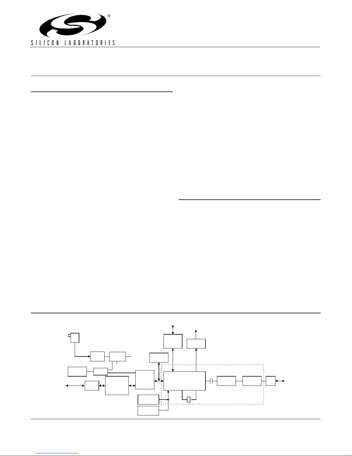
Functional Block Diagram
9 V dc at 300 mA ac
Adaptor
Rectifier
7.5–13.5 V dc or
peak ac
USB
Connector
UART
Filter
DB9
Rev. 0.6 2/05 Copyright © 2005 by Silicon Laboratories Si2493/57/34/15/04-EVB
USB I/F
Voltage
Regulator
5 V
RS-232
Transceivers
3.3 V
Access HDR
Interface
Selecti on
Jumpers
Push Button
Reset
Power-On
Reset
Direct
PCM Data/
Control
PCM
Interboard
Connector
Si2493/57/34/15/04
RESET XTALIXTALO
Audio
Out
Audio
Amplifier
Daughter Board Boundary
AOUT
*Si3010 for Si2404
Si3018*
Interface
Circuit
RJ-11
phone
line
Si2493/57/34/15/04
Global ISOmodem-EVB
1. Si2493/57/34/15/04-EVB Setup and
Evaluation
This section explains how to set up the Si2493/57/34/
15/04-EVB for evaluation as an RS-232 or USB
interface modem. Jumper settings, power connection,
PC/terminal connections, and terminal program
configuration settings are given. The initial modem
setup after power is applied as well as a basic tutorial
on modem operation are provided. Si2493/57/34/15/04EVB configurations for evaluating additional features
are discussed separately. See the Si2493/57/34/15 or
Si2404 data sheets and “AN93: Si2493/57/34/15/04/04
Modem Designer’s Guide” for complete details.
1.1. Si2493/57/34/15/04-EVB Quick Start—
RS-232 Interface
1. Set jumpers according to Figure 1 or Figure 2.
2. Connect:
DB-9 to PC COM 1 (with a pass-through cable).
RJ-11 to phone line or test box.
9 V ac adaptor (or USB cable).
3. Bring up:
Turn on power to modem.
Autobaud automatically adjusts modem DTE speed and
protocol.
4. Type “AT” followed by a carriage return.
Should echo “AT” and then an “OK”.
1.2. Si2493/57/34/15/04-EVB Quick Start—
USB Interface
1. Set jumpers according to Figure 3 or Figure 4.
2. Connect:
USB cable to PC
RJ-11 to phone line or test box
3. Download USB driver for your operating system from the
CD supplied with the evaluation board.
4. Install driver.
5. Bring up.
Reset the modem.
Autobaud automatically adjusts modem DTE speed and
protocol.
6. Type “AT” followed by a carriage return.
Should echo “AT” and then an “OK”.
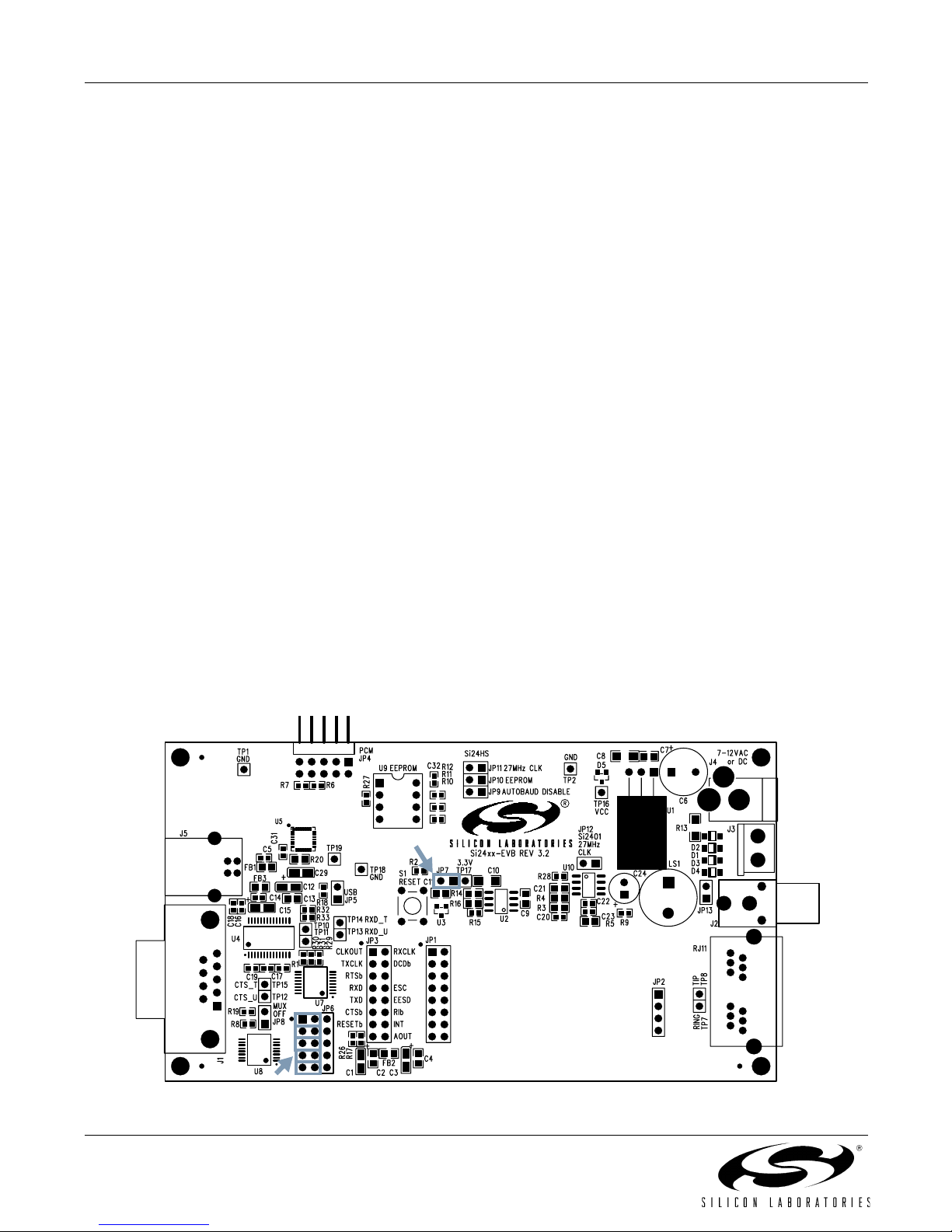
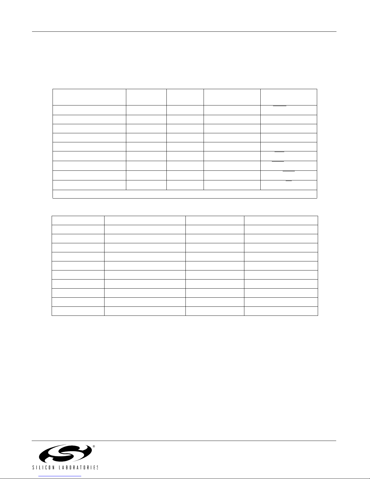
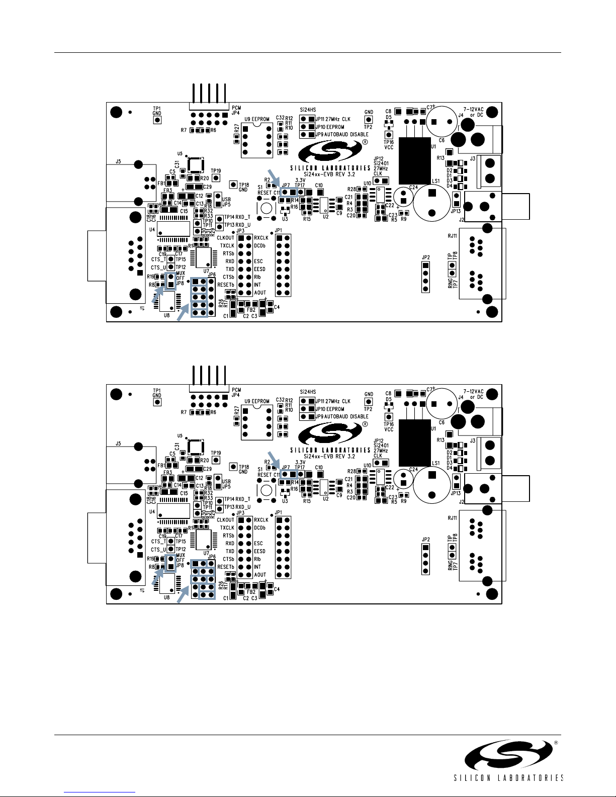
1.3. Jumper Settings
Check all jumper settings on the Si2493/57/34/15/04EVB before applying power. The standard factory
jumper settings for the FT package are shown in
Figure 1; the FS package is shown in Figure 2. These
settings configure the Si2493/57/34/15/04-EVB for RS232 serial operation with autobaud. Any standard
terminal program configured to communicate through a
PC COM port can be used to communicate with the
Si2493/57/34/15/04-EVB. The standard factory jumper
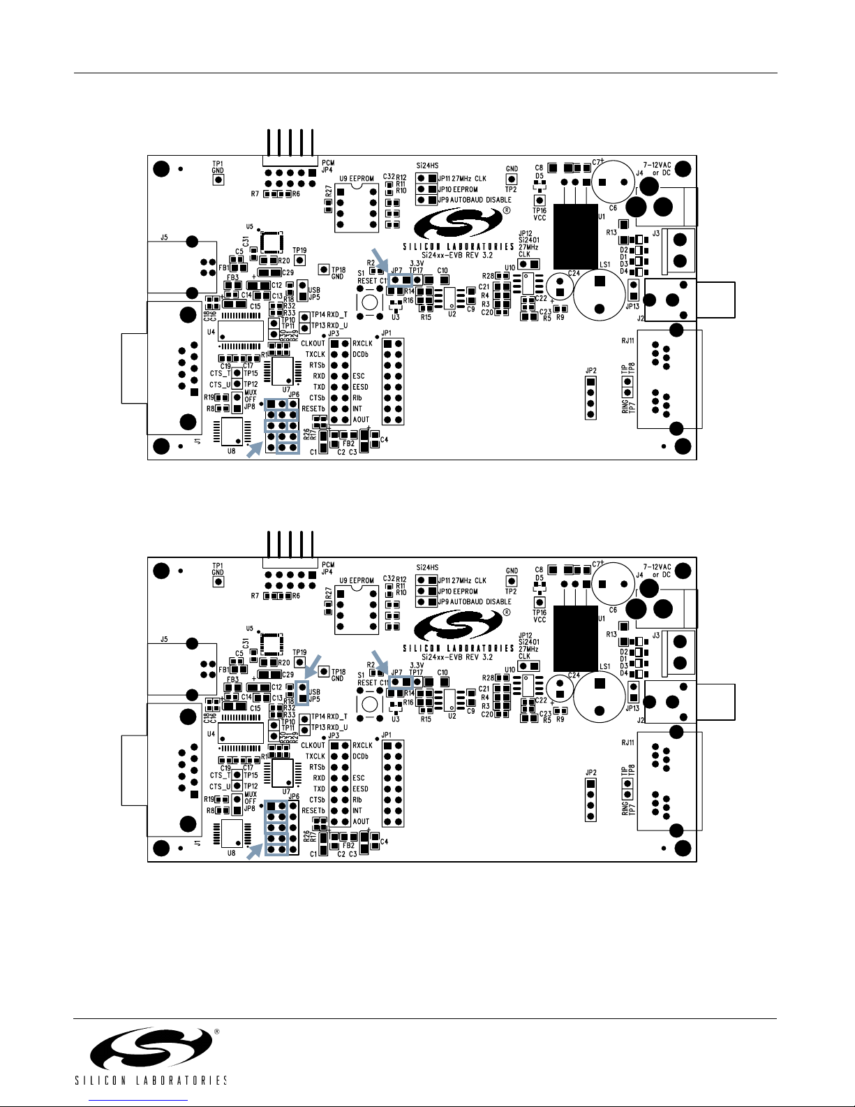
settings for USB operation with the FT package are
shown in Figure 3; the FS package is shown in Figure 4.
The only difference between RS-232 and USB jumper
settings is that JP5 must be installed to enable USB.
Figure 1. Standard Factory Jumper Settings—RS-232 Interface (Outlined in Gray) (FT Option)
2 Rev. 0.6
Si2493/57/34/15/04
Global ISOmodem-EVB
Figure 2. Standard Factory Jumper Settings—RS-232 Interface (Outlined in Gray) (FS Option)
Figure 3. Standard Factory Jumper Settings—USB Interface (Outlined in Gray) (FT Option)
Rev. 0.6 3

Si2493/57/34/15/04
Global ISOmodem-EVB
Figure 4. Standard Factory Jumper Settings—USB Interface (Outlined in Gray) (FS Option)
1.4. Power Requirements
The Si2493/57/34/15/04-EVB has an on-board diode
bridge, filter capacitor, and voltage regulator (U1).
Power can be supplied from any source capable of
providing 7.5 V–13 V dc or 7.5 V–13 V peak ac and at
least 100 mA. (Additional current may be required if a
speaker is connected for monitoring call progress
tones.) Power may be applied to the Si2493/57/34/15/
04-EVB through the screw terminals (J3), the 2 mm
power jack (J4), or the USB cable (even if the modem is
configured for RS-232 operation). The onboard fullwave rectifier and filter ensure the correct polarity is
applied to the Si2493/57/34/15/04-EVB. Daughter card
power is supplied through voltage regulator U2 by
connecting JP7, pins 1 and 2. Daughter card current
can be measured by connecting an ammeter between
JP7, pins 1 and 2. Failure to connect pins 1 and 2 of
JP7 through either a jumper or a low-impedance
ammeter may result in damage to the Si2493/57/34/15/
04-EVB.
1.5. Terminal and Line Connections
The Si2493/57/34/15/04 can be tested as a standard
serial data modem by connecting the Si2493/57/34/15/
04-EVB to a personal computer or other data terminal
equipment (DTE), phone line, and power. Connect a PC
serial port to the DB9 connector on the Si2493/57/34/
15/04-EVB with a pass-through cable. The RS-232
transceivers on the EVB can communicate with the DTE
at rates up to 1 Mbps. Any standard terminal program,
such as HyperTerminal or ProComm, running on a PC
communicates with the Si2493/57/34/15/04-EVB. The
standard factory jumper configuration has autobaud
enabled. Autobaud detects the DTE speed, data length,
parity, and number of stop bits.
If JP9 is installed, autobaud is disabled. Configure the
terminal emulation program to 19200 bps, eight data
bits, no parity, one stop bit, and hardware (CTS)
handshaking. Connect the RJ-11 jack on the Si2493/57/
34/15/04-EVB to an analog phone line or telephone line
simulator, such as a Teltone TLS 5.
1.6. Making Connections
With the terminal program properly configured and
running, apply power to the Si2493/57/34/15/04-EVB.
Type “AT<cr>”, and the modem should return “OK”
indicating the modem is working in the command mode
and communicating with the terminal. If the “OK”
response is not received, try resetting the modem by
pressing the manual reset switch (S1); then, again type
“AT<cr>.” Next, type “ATI6<cr>.” The modem should
respond with “2493”, “2457”, “2434”, “2415”, or “2404”
indicating the terminal is communicating with an Si2493,
Si2457, Si2434, Si2415, or Si2404.
Type “ATS0=2<cr>” to configure the modem to answer
on the second ring.
To take the modem off-hook, type “ATH1<cr>.” The
modem should go to the off-hook state, draw loop
4 Rev. 0.6

Si2493/57/34/15/04
Global ISOmodem-EVB
current, and respond with an “OK.” Next, type
“ATH<cr>” or “ATH0<cr>”, and the modem should hang
up (go on-hook) and stop drawing loop current.
To make a modem connection, type “ATDT(called
modem phone number)<cr>.” Once the connection is
established, a “CONNECT” message appears indicating
the two modems are in the data mode and
communicating. Typing on one terminal should appear
on the other terminal. To return to the command mode
without interrupting the connection between the two
modems, type “+++.” Approximately two seconds later,
“OK” appears. The modem is now in command mode
and accepts “AT” commands.Type “ATH” (or “ATH0”) to
terminate the data connection, or type “ATO” to return to
the data mode. After the ATO command, the modem
resumes the data connection and no longer accepts AT
commands.
1.7. EVB Part Numbers
The ISOmodem evaluation boards are offered in
multiple speeds and packaging options. The first four
numbers indicate the system-side device. The next two
letters indicate the system-side package (FS–Lead-free,
16-pin SOIC; FT–Lead-free, 24-pin TSSOP). The final
two numbers indicate the line-side device. See Figure 5.
Si2457FS18-EVB
LS Part Number (Si30xx)
SS Package
SS Part Number
Figure 5. EVB Part Number Example
2. Si2493/57/34/15/04-EVB
Functional Description
The Si2493/57/34/15/04-EVB is a multipurpose
evaluation system. The modem daughter card
illustrates the small size and few components required
to implement an entire controller-based modem with
global compatibility. The daughter card can be used
independently of, or in conjunction with, the
motherboard. The motherboard adds features that
enhance the ease of evaluating the many capabilities of
the Si2493/57/34/15/04 ISOmodem
2.1. Motherboard
The motherboard provides a convenient interface to the
Si2493/57/34/15/04 DC (daughter card). The versatile
power supply allows for a wide range of ac and dc
®
.
voltages to power the board. RS-232 transceivers and a
DB9 connector allow the Si2493/57/34/15/04-EVB to be
easily connected to a PC or other terminal device.
Jumper options allow direct access to the LVCMOS/TTL
level serial inputs to the Si2493/57/34/15/04, bypassing
the RS-232 transceivers or USB interface. This is
particularly useful for directly connecting the Si2493/57/
34/15/04 to embedded systems.
The Si24xxURT-EVB motherboard connects to the
daughter card through two connectors, JP1 and JP2.
JP1 is an 8x2 socket providing connection to all Si2493/
57/34/15/04 digital signals and regulated 3.3 V power
for the Si2493/57/34/15/04. The Si2493/57/34/15/04
digital signals appearing at JP1 (daughter card
interface) are LVCMOS and TTL compatible. The
Si2493/57/34/15/04 daughter card must be powered by
3.3 V. The motherboard is factory configured for 3.3 V
with JP7. JP2 is a 4x1 socket providing connection
between the daughter card and the RJ-11 phone jack.
2.1.1. Voltage Regulator/Power Supply
The input voltage to either J3 or J4 must be between 7.5
and 13.5 V dc or 7.5 and 13.5 V
motherboard includes a diode bridge (D1–D4) to guard
against a polarity reversal of the dc voltage or to rectify
an ac voltage. The power source must be capable of
continuously supplying at least 100 mA. C6 serves as a
filter cap for an ac input. The voltage regulator, U1,
provides 5 V for the motherboard and the input for
voltage regulator U2, which outputs 3.3 V for use on the
motherboard and to power the daughter card. Si24xxDC
power consumption can be measured by placing a
meter between pins 1 and 2 of JP7. The connection
between JP7 pins 1 and 2 must be made at all times
when power is applied to the evaluation board either
through a jumper block or a low-impedance meter to
avoid damage to the daughter card. Power is supplied
to U2 through D5 from the USB.
2.1.2. Reset Circuitry
The Si2493/57/34/15/04 requires a reset pulse to
remain low for at least 5.0 ms after the power supply
has stabilized during the powerup sequence or for at
least 5.0 ms during a power-on reset. Most production
Si2493/57/34/15/04 modem chipset applications require
that RESET
Si2493/57/34/15/04 operation modes, including
powerdown, require a hardware reset to recover.
The Si2493/57/34/15/04-EVB contains two reset
options, an automatic power-on reset device, U3
(DS1818) (default), and a manual reset switch (S1) to
permit resetting the chip without removing power. A
reset, regardless of the mechanism, causes all modem
settings to revert to factory default values. See
be controlled by the host processor. Certain
PEAK
ac. The
Rev. 0.6 5
Si2493/57/34/15/04
Global ISOmodem-EVB
Figure 13 on page 17 and Figure 15 on page 19 for the
reset circuit schematic.
2.1.3. DS1818
The DS1818 is a small, low-cost device that monitors
the voltage on V
V
drops below 3.0 V, the DS1818 provides a 220 ms
D
active-low reset pulse. On powerup, the DS1818 also
outputs an active low reset pulse for 220 ms after V
reaches 90% of the nominal 3.3 V value. The DS1818
outputs a 220 ms reset pulse any time the power supply
voltage exceeds the 3.3 V ±10% window.
2.1.4. Manual Reset
The manual reset switch (S1) performs a power-on
reset. This resets the Si2493/57/34/15/04 to factory
defaults without turning off power. If S1 is used in
conjunction with U3, pressing S1 activates the reset
monitor in the DS1818 and produces a 220 ms active
low reset pulse.
2.1.5. EEPROM Enable (FT Only)
Connecting JP10 enables the optional EEPROM, U9.
See “AN93: Si2457/Si2434/Si2415/Si2404 Modem
Designer’s Guide” for programming details.
2.1.6. Interface Selection
The serial interface of the Si2493/57/34/15/04-EVB can
be connected to a computer, terminal, embedded
system, or any other data terminal equipment (DTE) via
a standard RS-232 interface, USB interface, or through
a direct TTL serial interface.
The Si2493/57/34/15/04 can be tested as a standard
data modem by connecting the Si2493/57/34/15/04EVB to a personal computer or other DTE power supply
and a phone line. A PC can communicate with the
Si2493/57/34/15/04-EVB using a standard terminal
program, such as HyperTerm or ProComm.
Jumper settings determine how the Si2493/57/34/15/
04-EVB is connected to the DTE. Table 1 lists the
interface controlled by each motherboard jumper. See
Figure 14 on page 18 and Figure 24 on page 28.
and an external reset pushbutton. If
D
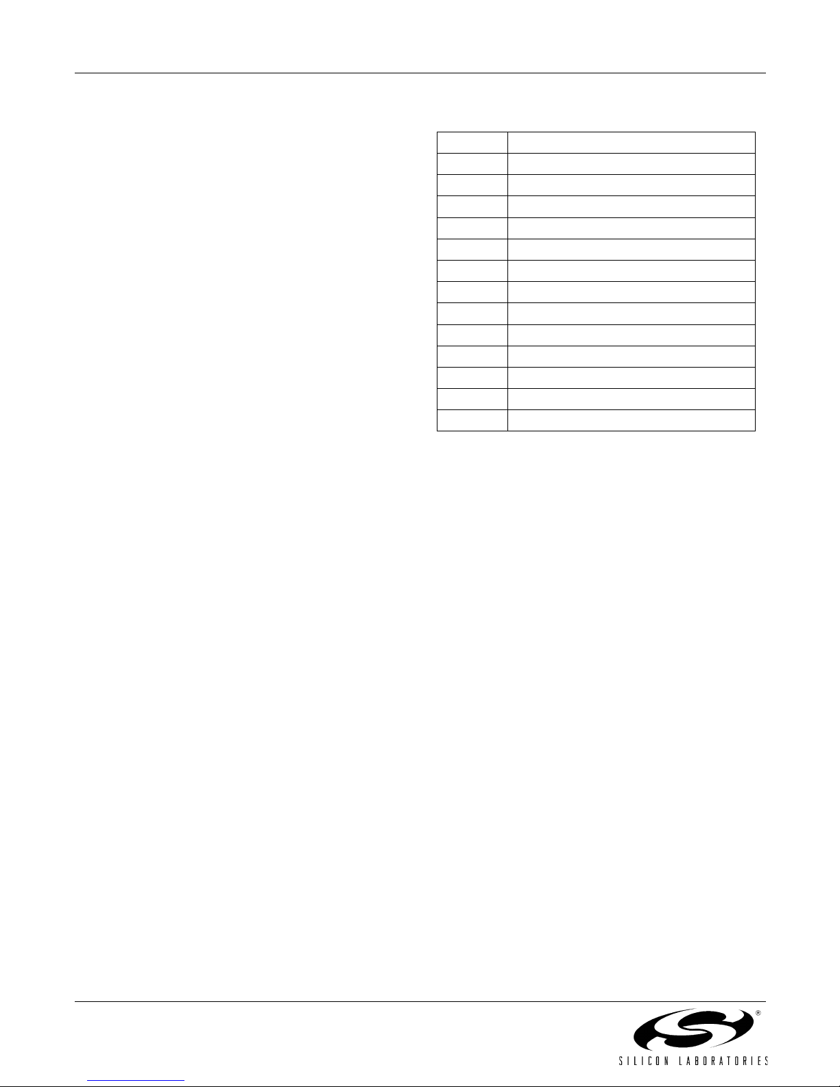
Table 1. Interface Selection Jumpers
Jumper Function
JP1 Daughter Card Digital Connector.
JP2 Daughter Card Phone Line Connector.
JP3 Direct Access Header.
D
JP4 PCM Interface.
JP5 USB Enable (RS-232 Disable).
JP6 Options.
JP7 3.3 V Power for Daughter Card.
JP8 Disable both RS-232 and USB.
JP9 Autobaud disable.
JP10 EEPROM enable.
JP11 Enable 27 MHz Clock option.
JP12 Not used.
JP13 On-board speaker enable.
2.1.7. RS-232 Interface
This operation mode uses the standard factory jumper
settings illustrated in Figure 1 on page 2. The Maxim
MAX3237 transceiver interfaces directly with the TTL
levels available at the serial interface of the Si2493/57/
34/15/04 and, using internal charge pumps, makes
these signals compatible with the RS-232 standard. The
RS-232 transceiver on the Si2493/57/34/15/04-EVB can
communicate at rates between 300 bps and 1 Mbps.
This simplifies the connection to PCs and other data
terminal equipment (DTE). The signals available on the
Si2493/57/34/15/04-EVB serial interface (DB9
connector) are listed in Table 2.
2.1.8. USB Interface
The USB cable connects to J5 on the motherboard and
provides both data and power. Installing a jumper on
JP5 enables the USB interface and disables the RS-232
interface. The USB interface is provided by U5. A USB
driver for this chip is available for most PC and MAC
operating systems on the CD.
2.1.9. Direct Access Interface
The motherboard supplies power through J3, J4, or
USB, power-on reset, and an RJ-11 jack for the modem.
The direct access interface (JP3) is used to connect the
motherboard to an embedded system. JP3 provides
access to all Si2493/57/34/15/04 signals available on
the daughter card. It is necessary to install a jumper on
JP8 to disable both the RS-232 and USB interface and
prevent signal contention. Leave the jumper between
JP7 pins 1 and 2. Figures 6 and 7 illustrate the jumper
settings required for the direct access mode using the
motherboard.
6 Rev. 0.6
Si2493/57/34/15/04
Global ISOmodem-EVB
2.1.10. PCM Interface (FT Only)
The Si2493/57/34/15/04 PCM interface is available on JP4. Table 3 lists the pin connections for JP4 designed to
connect directly to the Si3000SSI-EVB JP6.
Table 2. DB9 Pin Connections
J1 Name J1 Symbol J1 Pin Si2493/57/34/15/04
Pin
Carrier Detect CD 1
Received Data RXD 2 9 RXD
Transmit Data TXD 3 10 TXD
Data Terminal Ready DTR 4* See note ESC/RI
Signal Ground SG 5 6 GND
Data Set Ready DSR 6* See note
Ready to Send RTS 7* See note
Clear to Send CTS 8 11
Ring Indicator RD 9
*Note: JP6 jumper option.
*
*
See note
17
Si2493/57/34/15/04
Name
DCD
/EESD
INT
/AOUT
RTS
/RXCLK
CTS
RI
Table 3. JP 4 PCM Interface Pin Connections
JP 4 Pin Board Signal Si24xx Pin Si24xx Signal
1 CLKOUT_H 3 CLKOUT
2 TXCLK_H 4 FSYNC
3 GND 6, 20 GND
4 GND 6, 20 GND
5 RXCLK_H 24 SDO
6 EESD_H 18 SDI
7 RESETb 12 RESET*
8 3.3 V 5, 21 VD3.3
9 GND 6, 20 GND
10 VCC (+5 V)
Rev. 0.6 7
Si2493/57/34/15/04
Global ISOmodem-EVB
Figure 6. Jumper Settings for Direct Access Interface (FT Option)
Figure 7. Jumper Settings for Direct Access Interface (FS Option)
8 Rev. 0.6
Si2493/57/34/15/04
Global ISOmodem-EVB
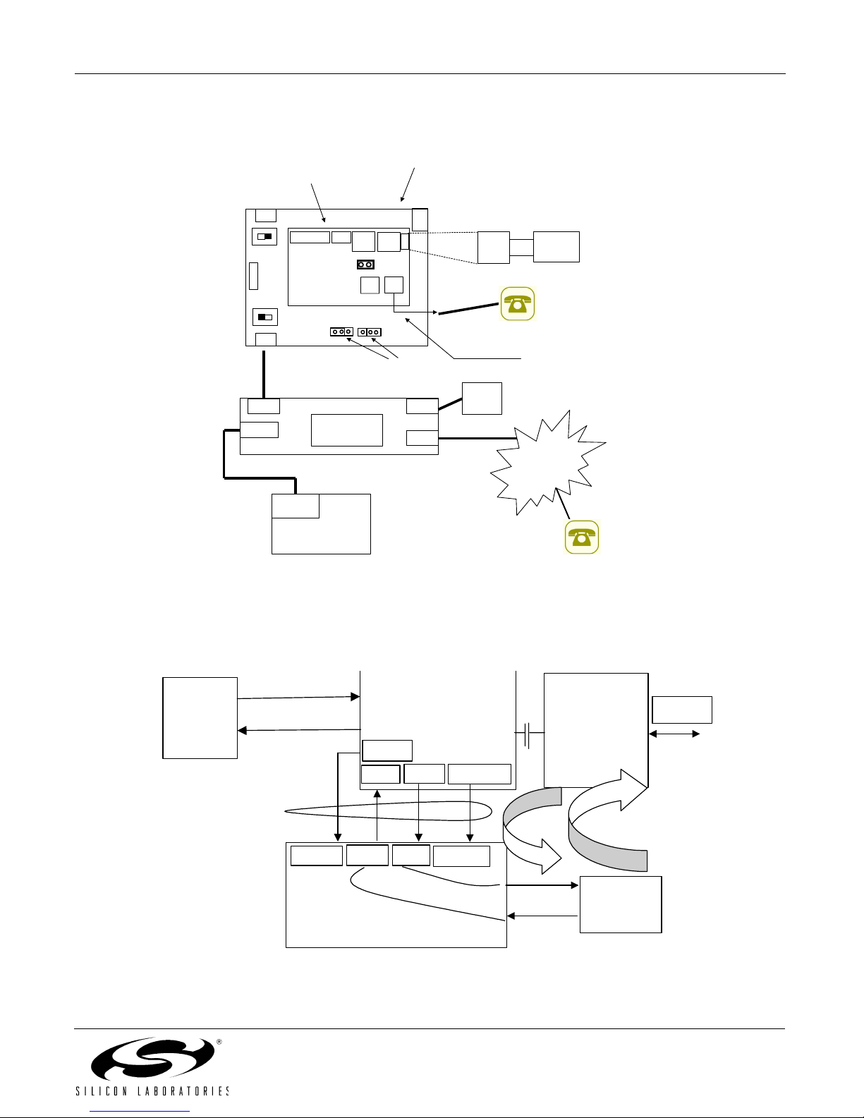
The block diagram in Figure 8 shows how the two evaluation boards are connected to demonstrate voice mode
operation.
Si3000SSI-EVB Motherboard
1
2
Direct Connection
RS232 Si24xx-DC
Si3000 Daughterboard
JP5
Speaker
2
SW2
JP4
SW3
1
JP6
JP4
Line
Mic
JP4
Si24xx-EVB
Line
Out
In
RJ11
Note M1 and M0
jumper settings.
Leave J3 unconnected.
Power is provided
through JP 6 connector.
J
3
J
6
J4
RJ11
J6 of Daughterboard
12V
GND
Power
Adapter
External
+12V
Supply
Use telephone in off
hook position to emulate
600 Ω Handset. Not all
handsets are
implemented as 2 wire
anymore.
Connect the telephone to RJ 11
(right side) on the Si3000
Daughterboard, NOT to the
RJ11 on motherboard. Look for
silk screen marking "HDST".
WAN
COM 1
Telephone
Windows PC
Figure 8. Connection Block Diagram for Si3000SSI-EVB and Si24XXURT-EVB
2.1.11. Voice Mode
The Si3000 is used in conjunction with the Si2493/57/34/15/04 to transmit and receive 16-bit voice samples to and
from telephone lines as shown in Figure 9.
AT commands
HOST
Responses
TDMA Interface
FSYNC MCLK
Si2457 Modem
FSYNC
SDI
SDO
SDISDO
DAA
CLKOUT
2- wire
Handset
Si3000 Voice Codec
Figure 9. Voice Mode Block Diagram
Rev. 0.6 9
Si2493/57/34/15/04
Global ISOmodem-EVB
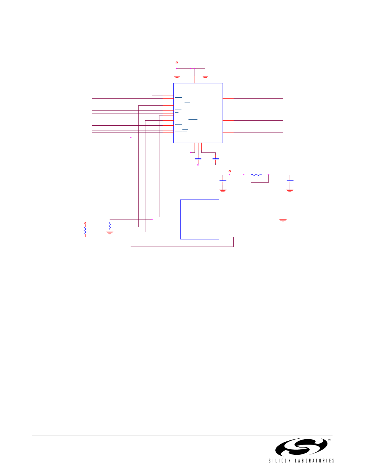
Figure 10 shows the actual circuit connection between the Si2493/57/34/15/04 and the Si3000.
VDD
21
VD3.3
VD 3.3
CLKIN/XTALI
GND6VDA
GND
7
19
20
C51 C53
C52
U3
XTALO
C1A
C2A
VDB
Si2493/57/34/15/04
1
2
14
13
R61
VDD
C66
0.1 uF
0
XTALI
XTALO
C1A
C1B
NOTE: D6 (PIN 4) MUST NOT HAVE PULLDOWN RESISTOR
DCDb
ESC
AOUT
INTb
RIb
RTSb
RXD
TXD
CTSb
RESETb
24
23
22
15
4
16
17
18
3
8
9
10
11
12
C50
EECLK/D5
DCD/D4
ESC/D3
AOUT/INT
D6
INT/D0
RI/D1
EESD/D2
CLKOUT/EECS/A0
RTS/D7
RXD/RD
TXD/WR
CTS/CS
RESET
5
C68
0.1 uF
SPKR_R
MIC_BIAS
HDST
VDD
R62
47 k
R63
47 k
1
SPKR_R
2
MIC_BIAS
3
HDST
4
SDI
5
SDO
6
FSYNC
7
MCLK
8
SCLK
Si3000
SPKR_L
LINEO
MIC_IN
RESET
LINEI
16
15
14
GND
13
VA
12
VD
11
10
9
SPKR_L
LINEO
LINEI
MIC_IN
Figure 10. Circuit Connection between the Si2493/57/34/15/04 and the Si3000
To use voice mode register U71 and data memory location 0x0059 must be properly configured.
Setting data memory 0x0059 = 0x0001 enables the Si24XX TDMA interface. When U71 is set to the value 0x0011
a 16-bit voice sample will be transmitted from the Si3000 through the Si2493/57/34/15/04 and DAA to the remote
device. Likewise, an analog signal from the remote device will pass through the DAA where it is converted to a 16bit voice sample, the Si24XX and finally the Si3000 where it is converted back to the analog receive signal.
In this example, the Si3000 has its digital TDMA interface configured as the Slave Serial Mode by adding a 50 kΩ
pull-down resistor to SDO pin and a pull-up 50 kΩ resistor to SCLK pin. In this mode, the Si3000’s MCLK is driven
by the 2048 kHz clock from Si2493/57/34/15/04. The FSYNC has an 8 kHz pulse input. The bit clock is 2048/
8 = 256 bits per frame sync. Refer to the Si3000 documentation for further details.
To send control information to the Si3000, the Si2493/57/34/15/04 modem chip provides a PCM control port
0x004B that allows the user to send control words across by using the AT memory write command. See Table 4. for
details. Wait for the “OK” (approximately 300 ms after each command). When a connection is established, the “AT.”
command is used to generate the DTMF tone of a number; For example, AT.3<CR> will generate a number 3
DTMF tone without the need for an external DTMF generator. See “Voice Mode Example” for details.
10 Rev. 0.6
Si2493/57/34/15/04
Global ISOmodem-EVB
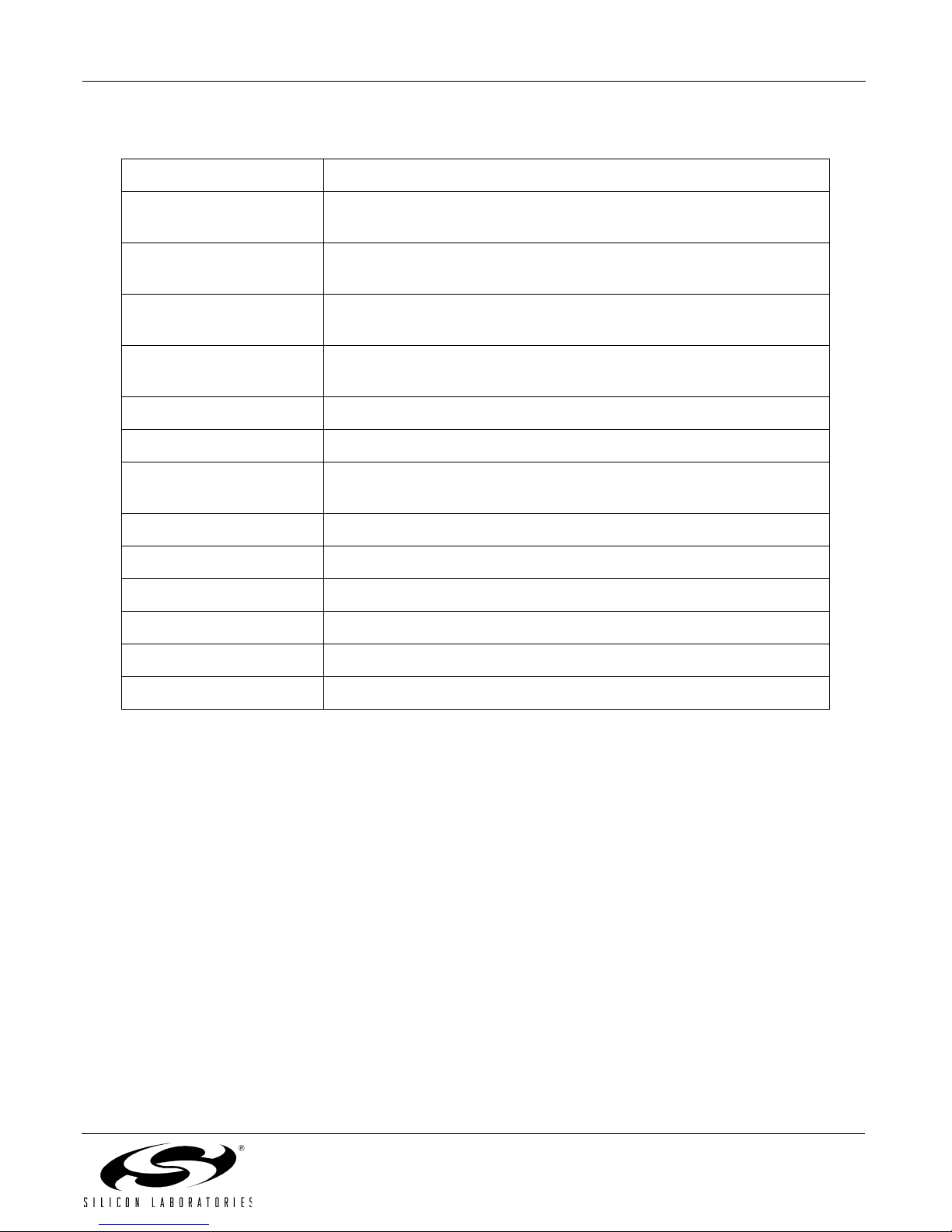
Table 4. Voice Commands
AT Commands Purposes
AT:U71,11 Configure modem to send/receive data in linear mode to/from Si3000
interface
AT*Y254:W0059,7785 Enable Si2457 modem TDMA’s interface by setting LSBit of memory
0x0059
AT*Y254:W004B,011C Write to Si3000 Control Reg1: Line Driver, Handset Driver, and Micro-
phone Bias Normal Operations are enabled.
AT*Y254:W004B,0200 Write to Si3000 Control Reg2: HPF enabled, PLL divided by 5, Digital
Loopback Off
AT*Y254:W004B,0300 Write to Si3000 Control Reg3: PLL Divider N1
AT*Y254:W004B,0400 Write to Si3000 Control Reg4: PLL Divider M1
AT*Y254:W004B,055A Write to Si3000 Control Reg5: Line-In, Mic-In, Handset-In, FIR are acti-
vated.
AT*Y254:W004B,067F Write to Si3000 Control Reg6: Line-Out, Handset-Out are activated.
AT*Y254:W004B,075F Write to Si3000 Control Reg7: SPKR_L, SPLR_R are activated.
ATH1 Off-hook command for calling
AT.1 Dial individual number 1
AT.0 Dial individual number 0
AT.4 Dial individual number 4 and wait for answer
Rev. 0.6 11
 Loading...