

Page 1
Si10xx-DK
Si1000 AND Si1010 DEVELOPMENT KIT USER’S G UIDE
1. Relevant Devices
The Si1000 and Si1010 Development Kits are intended as development platforms for the microcontrollers in the
Si100x and Si101x MCU family, respectively. The members of these MCU families include Si1000, Si1001, Si1002,
Si1003, Si1004, Si1005, Si1010, Si1011, Si1012, Si1013, Si1014, and Si1015. Each kit consists of a motherboard
and daughtercard. The daughtercard included in the kit is configured for high band (868/915 MHz) and up to
+20 dBm transmit power. Additional daughtercards may be purchased separately for low band or low transmit
power applications.
2. Kit Contents
The Si1000 and Si1010 Development Kit contains the following items:
Si1000 motherboard which supports all Si10xx series daughtercards
Si1000 or Si1010 daughtercard (Si1000 or Si1010 MCU pre-soldered on the daughtercard)
Si10xx Development Kit Quick-Start Guide
Silicon Laboratories IDE and Product Information CD-ROM. CD content includes the following:
Silicon Laboratories Integrated Development Environment (IDE)
Keil 8051 Development Tools (macro assembler, linker, evaluation C compiler)
Source code examples and register definition files
Documentation
Si1000 and Si1010 Development Kit User’s Guide (this document)
AC to DC Power Adapter
USB Debug Adapter (USB to Debug Interface)
2 USB cables
2 AAA batteries
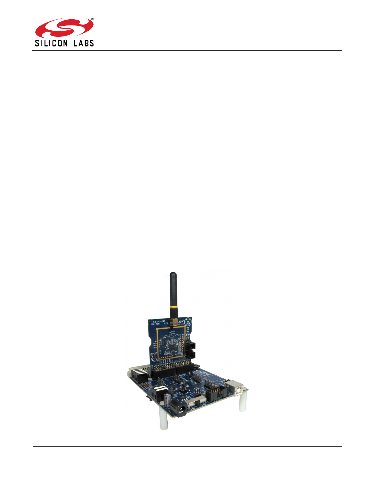
Figure 1. Si1000 Motherboard with Si1000 Daughtercard
Rev. 0.1 Copyright © 2014 by Silicon Laboratories Si10xx-DK
Page 2

Si10xx-DK
3. Software Overview
All software required to develop firmware and communicate with the target microcontroller is included in the CDROM. The CD-ROM also includes other useful software.
Below is the software necessary for firmware development and communication with the target microcontroller:
Silicon Laboratories Integrated Development Environment (IDE)
Keil 8051 Development Tools (macro assembler, linker, evaluation C compiler)
Other useful software that is provided in the CD-ROM includes the following:
Configuration Wizard 2
Keil μVision Drivers
CP210x USB to UART Virtual COM Port (VCP) Drivers
3.1. Software Installation
The included CD-ROM contains the Silicon Laboratories Integrated Development Environment (IDE), Keil software
8051 tools and additional documentation. Insert the CD-ROM into your PC’s CD-ROM drive. An installer will
automatically launch allowing you to install the IDE software or read documentation by clicking buttons on the
Installation Panel. If the installer does not automatically start when you insert the CD-ROM, run autorun.exe found
in the root directory of the CD-ROM. Refer to the ReleaseNotes.txt file on the CD-ROM for the latest information
regarding known problems and restrictions. After installing the software, see the following sections for information
regarding the software and running one of the demo applications.
3.2. CP210x USB to UART VCP Driver Installation
The Si10xx Target Board includes a Silicon Laboratories CP2103 USB-to-UART Bridge Controller. Device drivers
for the CP2103 need to be installed before PC software such as HyperTerminal can communicate with the target
board over the USB connection. If the "Install CP210x Drivers" option was selected during installation, this will
launch a driver “unpacker” utility.
1. Follow the steps to copy the driver files to the desired location. The default directory is C:\SiLabs\MCU\CP210x.
2. The final window will give an option to install the driver on the target system. Select the “Launch the CP210x
VCP Driver Installer” option if you are ready to install the driver.
3. If selected, the driver installer will now launch, providing an option to specify the driver installation location. After
pressing the “Install” button, the installer will search your system for copies of previously installed CP210x
Virtual COM Port drivers. It will let you know when your system is up to date. The driver files included in this
installation have been certified by Microsoft.
4. If the “Launch the CP210x VCP Driver Installer” option was not selected in step 3, the installer can be found in
the location specified in step 2, by default C:\SiLabs\MCU\CP210x\Windows_2K_XP_S2K3_Vista. At this
location run CP210xVCPInstaller.exe.
5. To complete the installation process, connect the included USB cable between the host computer and the USB
connector (P3) on the Si10xx Target Board. Windows will automatically finish the driver installation. Information
windows will pop up from the taskbar to show the installation progress.
6. If needed, the driver files can be uninstalled by selecting “Silicon Laboratories CP210x USB to UART Bridge
(Driver Removal)” option in the “Add or Remove Programs” window.
3.3. Silicon Laboratories IDE
The Silicon Laboratories IDE integrates a source-code editor, a source-level debugger, and an in-system Flash
programmer. See Section 5. "Using the Keil Software 8051 Tools with the Silicon Laboratories IDE‚" on page 8 for
detailed information on how to use the IDE. The Keil Evaluation Toolset includes a compiler, linker, and assembler
and easily integrates into the IDE. The use of third-party compilers and assemblers is also supported.
3.3.1. IDE System Requirements
The Silicon Laboratories IDE requirements:
Pentium-class host PC running Microsoft Windows 2000 or newer
One available USB port
64 MB RAM and 40 MB free HD space recommended
2 Rev. 0.1
Page 3
Si10xx-DK
3.3.2. 3rd Party Toolsets
The Silicon Laboratories IDE has native support for many 8051 compilers. The full list of natively supported tools is
as follows:
Keil
IAR
Raisonance
Tasking
Hi-Tech
SDCC
The demo applications for the Si10xx target board are written to work with the Keil and SDCC toolsets.
3.4. Keil Evaluation Toolset
3.4.1. Keil Assembler and Linker
The Keil demonstration toolset assembler and linker place no restrictions on code size.
3.4.2. Keil Evaluation C51 C Compiler
The evaluation version of the C51 compiler is the same as the full version with the following limitations: Maximum
4 kB code generation, and there is no floating point library included. When installed from the CD-ROM, the C51
compiler is initially limited to a code size of 2 kB, and programs start at code address 0x0800. Refer to “AN104:
Integrating Keil Tools into the Silicon Labs IDE" for instructions to change the limitation to 4 kB and have the
programs start at code address 0x0000.
3.5. Configuration Wizard 2
The Configuration Wizard 2 is a code generation tool for all of the Silicon Laboratories devices. Code is generated
through the use of dialog boxes for each of the device's peripherals.
Figure 2. Configuration Wizard 2 Utility
Rev. 0.1 3
Page 4
Si10xx-DK
The Configuration Wizard utility helps accelerate development by automatically generating initialization source
code to configure and enable the on-chip resources needed by most design projects. In just a few steps, the wizard
creates complete startup code for a specific Silicon Laboratories MCU. The program is configurable to provide the
output in C or assembly language. For more information, refer to the Configuration Wizard documentation.
Documentation and software is available on the kit CD and from the downloads webpage: www.silabs.com/
mcudownloads.
3.6. Silicon Labs Battery Life Estimator
The Battery Life Estimator is a system design tool for battery operated devices. It allows the user to select the type
of battery they are using in the system and enter the supply current profile of their application. Using this
information, it performs a simulation and provides an estimated system operating time. The Battery Life Estimator
is shown in Figure 3.
Figure 3. Battery Life Estimator Utility
From Figure 3, the two inputs to the Battery Life Estimator are battery type and discharge profile. The utility
includes battery profiles for common battery types such as AAA, AA, A76 Button Cell, and CR2032 coin cell. The
discharge profile is application-specific and describes the supply current requirements of the system under various
supply voltages and battery configurations. The discharge profile is independent of the selected power source.
Several read-only discharge profiles for common applications are included in the pulldown menu. The user may
also create a new profile for their own applications.
4 Rev. 0.1
Page 5
Si10xx-DK
To create a new profile:
1. Select the profile that most closely matches the target application or choose the "Custom Profile".
2. Click Manage
3. Click Duplicate
4. Click Edit
Profiles may be edited with the easy-to-use GUI (shown in Figure 4).
Figure 4. Battery Life Estimator Discharge Profile Editor
The Discharge Profile Editor allows the user to modify the profile name and description. The four text entry boxes
on the left hand side of the form allow the user to specify the amount of time the system spends in each power
mode. On the right hand side, the user may specify the supply current of the system in each power mode.
Rev. 0.1 5
Page 6
Si10xx-DK
Since supply current is typically dependent on supply voltage, the discharge profile editor provides two columns for
supply current. The V2 and V1 voltages at the top of the two columns specify the voltages at which the current
measurements were taken. The Battery Life Estimator creates a linear approximation based on the input data and
is able to feed the simulation engine with an approximate supply current demand for every input voltage.
The minimum system operating voltage input field allows the system operating time to stop increasing when the
simulated battery voltage drops below a certain threshold. This is primarily to allow operating time estimates for
systems that cannot operate down to 1.8 V, which is the voltage of two fully drained single-cell batteries placed in
series.
The wakeup frequency box calculates the period of a single iteration through the four power modes and displays
the system wake up frequency. This is typically the "sample rate" in low power analog sensors.
Once the battery type and discharge profile is specified, the user can click the "Simulate" button to start a new
simulation. The simulation engine calculates the estimated battery life when using one single-cell battery, two
single-cell batteries in series, and two single-cell batteries in parallel. Figure 5 shows the simulation output window.
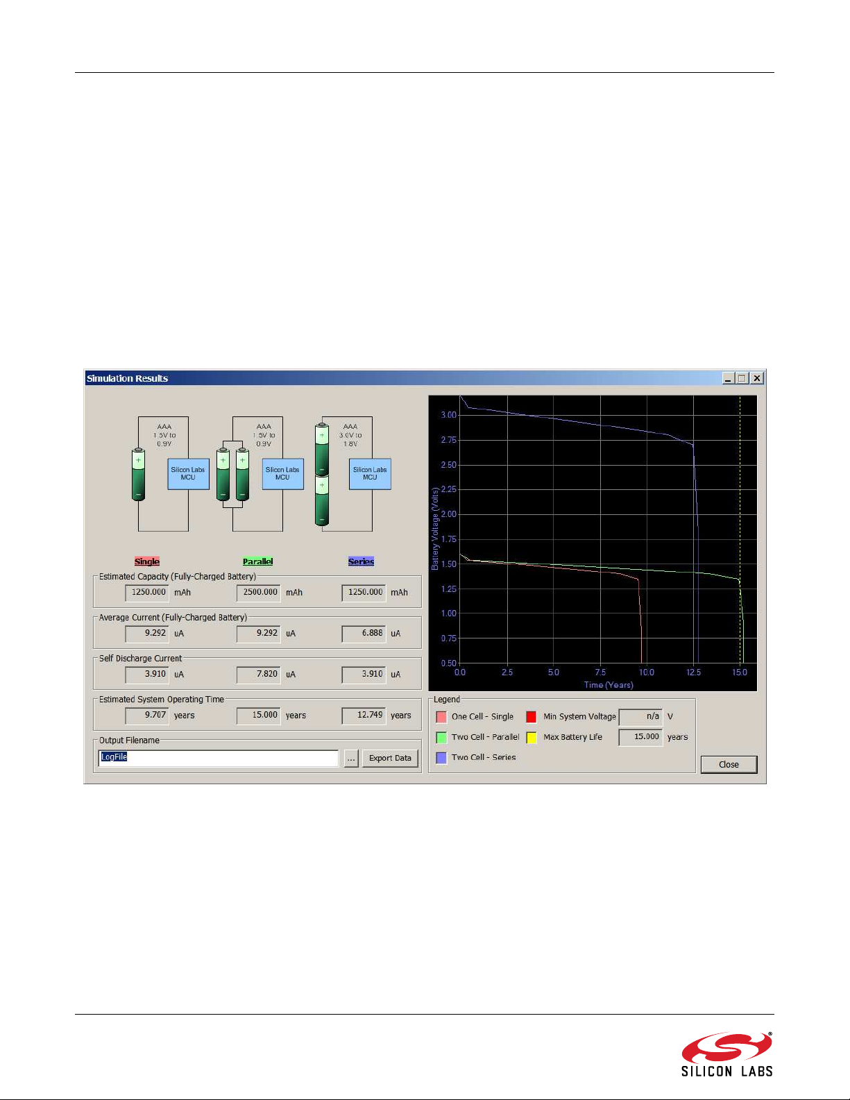
Figure 5. Battery Life Estimator Utility Simulation Results Form
The primary outputs of the Battery Life Estimator are an estimated system operating time and a simulated graph of
battery voltage vs. time. Additional outputs include estimated battery capacity, average current, self-discharge
current, and the ability to export graph data to a comma delimited text file for plotting in an external graphing
application.
6 Rev. 0.1
Page 7
Si10xx-DK
3.7. Keil μVision2 and μVision3 Silicon Laboratories Drivers
As an alternative to the Silicon Laboratories IDE, the μVision debug driver allows the Keil μVision2 and μVision3
IDEs to communicate with Silicon Laboratories’ on-chip debug logic. In-system Flash memory programming
integrated into the driver allows for rapid updating of target code. The μVision2 and μVision3 IDEs can be used to
start and stop program execution, set breakpoints, check variables, inspect and modify memory contents, and
single-step through programs running on the actual target hardware. For more information, refer to the μVision
driver documentation. The documentation and software are available on the kit CD and from the downloads
webpage:
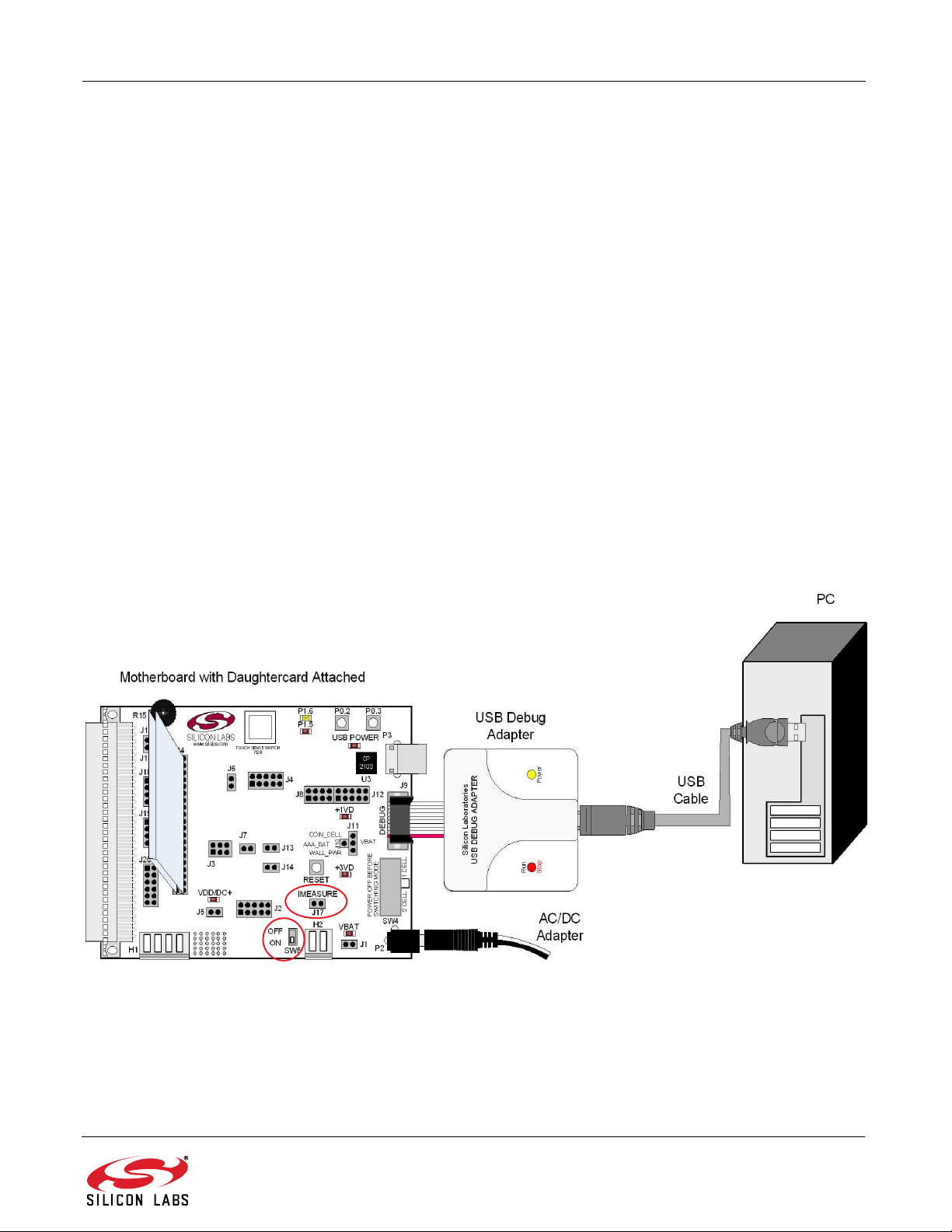
4. Hardware Setup using a USB Debug Adapter
The motherboard is connected to a PC running the Silicon Laboratories IDE via the USB Debug Adapter as shown
in Figure 6.
1. Connect the USB Debug Adapter to the DEBUG connector on the motherboard with the 10-pin ribbon cable.
2. Connect one end of the USB cable to the USB connector on the USB Debug Adapter.
3. Verify that a shorting block is installed on J17 and that SW5 is in the ON position.
4. Connect the other end of the USB cable to a USB Port on the PC.
5. Connect the ac/dc power adapter to power jack P1 on the target board (Optional).
Notes:
Use the Reset button in the IDE to reset the target when connected using a USB Debug Adapter.
Remove power from the target board and the USB Debug Adapter before connecting or disconnecting the
ribbon cable from the target board. Connecting or disconnecting the cable when the devices have power can
damage the device and/or the USB Debug Adapter.
www.silabs.com/mcudownloads.
Figure 6. Hardware Setup using a USB Debug Adapter
Rev. 0.1 7
Page 8

Si10xx-DK
5. Using the Keil Software 8051 Tools with the Silicon Laboratories IDE
To perform source-level debugging with the IDE, configure the Keil 8051 tools to generate an absolute object file in
the OMF-51 format with object extensions and debug records enabled. Build the OMF-51 absolute object file by
calling the Keil 8051 tools at the command line (e.g., batch file or make file) or by using the project manager built
into the IDE. The default configuration when using the Silicon Laboratories IDE project manager enables object
extension and debug record generation.
the “SiLabs\MCU\Documentation\ApplicationNotes” directory on the CD-ROM for additional information on using the
Keil 8051 tools with the Silicon Laboratories IDE.
To build an absolute object file using the Silicon Laboratories IDE project manager, you must first create a project.
A project consists of a set of files, IDE configuration, debug views, and a target build configuration (list of files and
tool configurations used as input to the assembler, compiler, and linker when building an output object file).
The following sections illustrate the steps necessary to manually create a project with one or more source files,
build a program, and download it to the target in preparation for debugging. (The IDE will automatically create a
single-file project using the currently open and active source file if you select Build/Make Project before a project is
defined.)
5.1. Creating a New Project
1. Select ProjectNew Project to open a new project and reset all configuration settings to default.
2. Select FileNew File to open an editor window. Create your source file(s) and save the file(s) with a
recognized extension, such as .c, .h, or .asm, to enable color syntax highlighting.
3. Right-click on “New Project” in the Project Window. Select Add files to project. Select files in the file browser
and click Open. Continue adding files until all project files have been added.
4. For each of the files in the Project Window that you want assembled, compiled and linked into the target build,
right-click on the file name and select Add file to build. Each file will be assembled or compiled as appropriate
(based on file extension) and linked into the build of the absolute object file.
5. If a project contains a large number of files, the “Group” feature of the IDE can be used to organize. Right-click
on “New Project” in the Project Window. Select Add Groups to project. Add pre-defined groups or add
customized groups. Right-click on the group name and choose Add file to group. Select files to be added.
Continue adding files until all project files have been added.
Refer to
"AN104: Integrating Keil 8051 Tools into the Silicon Labs IDE"
in
5.2. Building and Downloading the Program for Debugging
1. Once all source files have been added to the target build, build the project by clicking on the Build/Make Project
button in the toolbar or selecting ProjectBuild/Make Project from the menu.
Note: After the project has been built the first time, the Build/Make Project command will only build the files that
have been changed since the previous build. To rebuild all files and project dependencies, click on the Rebuild
All button in the toolbar or select ProjectRebuild All from the menu.
2. Before connecting to the target device, several connection options may need to be set. Open the Connection
Options window by selecting OptionsConnection Options... in the IDE menu. First, select the appropriate
adapter in the “Serial Adapter” section. Next, the correct “Debug Interface” must be selected. Si100x-Si101x
family devices use the Silicon Labs 2-wire (C2) debug interface. Once all the selections are made, click the OK
button to close the window.
3. Click the Connect button in the toolbar or select DebugConnect from the menu to connect to the device.
4. Download the project to the target by clicking the Download Code button in the toolbar.
Note: To enable automatic downloading if the program build is successful select Enable automatic connect/
download after build in the ProjectTarget Build Configuration dialog. If errors occur during the build process,
the IDE will not attempt the download.
5. Save the project when finished with the debug session to preserve the current target build configuration, editor
settings and the location of all open debug views. To save the project, select ProjectSave Project As... from
the menu. Create a new name for the project and click on Save.
8 Rev. 0.1
Page 9

Si10xx-DK
6. Example Source Code
Example source code and register definition files are provided in the “SiLabs\MCU\Examples\Si100x\” or the
“SiLabs\MCU\Examples\Si101x\” default directory during IDE installation. These files may be used as a template
for code development. Example applications include a blinking LED example which configures the LED on the
motherboard to blink at a fixed rate.
6.1. Register Definition Files
Register definition files Si1000_defs.h and Si1010_defs.h define all SFR registers and bit-addressable control/
status bits. A macro definition header file compiler_defs.h is also included, and is required to be able to use the
Si1000 and Si1010_defs.h header file with various tool chains. These files are installed into the
“SiLabs\MCU\Examples\Si100x\Header_Files\” and “SiLabs\MCU\Examples\Si101x\Header_Files\” directories
during IDE installation by default. The register and bit names are identical to those used in the Si100x and Si101x
data sheets. These register definition files are also installed in the default search path used by the Keil Software
8051 tools. Therefore, when using the Keil 8051 tools included with the development kit (A51, C51), it is not
necessary to copy a register definition file to each project’s file directory.
6.2. Blinking LED Example
The example source files Si100x_Blinky.asm and Si101x_Blinky.c installed in the default directories
“SiLabs\MCU\Examples\Si100x\Blinky” and “SiLabs\MCU\Examples\Si101x\Blinky” show examples of several
basic MCU functions. These include disabling the watchdog timer (WDT), configuring the Port I/O crossbar,
configuring a timer for an interrupt routine, initializing the system clock, and configuring a GPIO port pin. When
compiled/assembled and linked this program flashes the LED on the Si1000 Motherboard about five times a
second using the interrupt handler with an on-chip timer.
6.3. RF Examples
The Si100x and Si101x MCUs support RF communication. Examples of RF communication using the Si100x and
Si101x products are described in Application Note AN474. The source code for the RF examples is installed into
the “SiLabs\MCU\Examples\Si100x\EZRadioPRO\” and “SiLabs\MCU\Examples\Si101x\EZRadioPRO\” during
IDE installation. The most basic example is the TxTone example. When downloaded and run on the MCU, a
915 MHz tone will be generated from the EZRadioPRO peripheral output.
Rev. 0.1 9
Page 10

Si10xx-DK
7. Using the Si1000 Motherboard with the Wireless Development Suite
The Si1000 motherboard is supported by the Wireless Development Suite. Some features of the Wireless
Development Suite will be disabled when connected to an Si1000 motherboard. See the Wireless Development
Suite documentation for details. When using the Wireless Development Suite, the following configurations are
required:
J18 - shorting blocks should be closed if using an Si1000/1/2/3/4/5 device and open otherwise.
J19 - shorting blocks should be closed if using an Si1010/1/2/3/4/5 device and open otherwise.
J20 - shorting blocks should be closed
J12 - 3 shorting blocks (closest to USB connector) should be closed to enable UART communication.
Firmware is currently in development to allow the Si10xx daughtercards to connect to the Wireless Development
Suite through the Si1000 Motherboard.
8. Using Si10xx Daughtercards with the Wireless Development Suite
To enable all the features of the Wireless Development Suite, the Si10xx daughtercards may be used directly with
wireless development suite, without an Si1000 motherboard. The Si10xx daughtercards must be programmed with
“pass-through” firmware to make them appear as fixed-function, stand-alone EZRadioPRO devices such as the
Si4430/1/2/3. An SDBC-DK3 development kit is required to connect to the Wireless Development Suite in this
mode.
To program the Si10xx daughtercards for this mode, download the following hex file to the daughtercard:
For Si100x daughtercards:
C:\Silabs\MCU\Examples\Si100x\EZRadioPRO\SPI_PassThrough\SPI_PassThrough.hex
For Si101x daughtercards:
C:\Silabs\MCU\Examples\Si101x\EZRadioPRO\SPI_PassThrough\SPI_PassThrough.hex
After the “pass-through” code is downloaded to the daughtercard, it may be used as a standard daughercard for
the SDBC-DK3 development kit. See the SDBC-DK3 documentation for more details.
9. Using the Si1000 Motherboard with a CP240x LCD Development Board
The Si1000 motherboard supports the CP2400 and CP2401 development boards for developing LCD applications.
When using an LCD development board, the following configurations are required:
J18 - shorting blocks should be closed if using an Si1000/1/2/3/4/5 device and open otherwise.
J19 - shorting blocks should be closed if using an Si1010/1/2/3/4/5 device and open otherwise.
J20 - shorting blocks should be open
When a CP240x development board is connected to the Si1000 motherboard, the Port I/O usage matrix shown in
Figure 7 should be used for software development.
10 Rev. 0.1
Page 11

Si10xx-DK
Figure 7. Port I/O Usage Matrix
Rev. 0.1 11
Page 12
Si10xx-DK
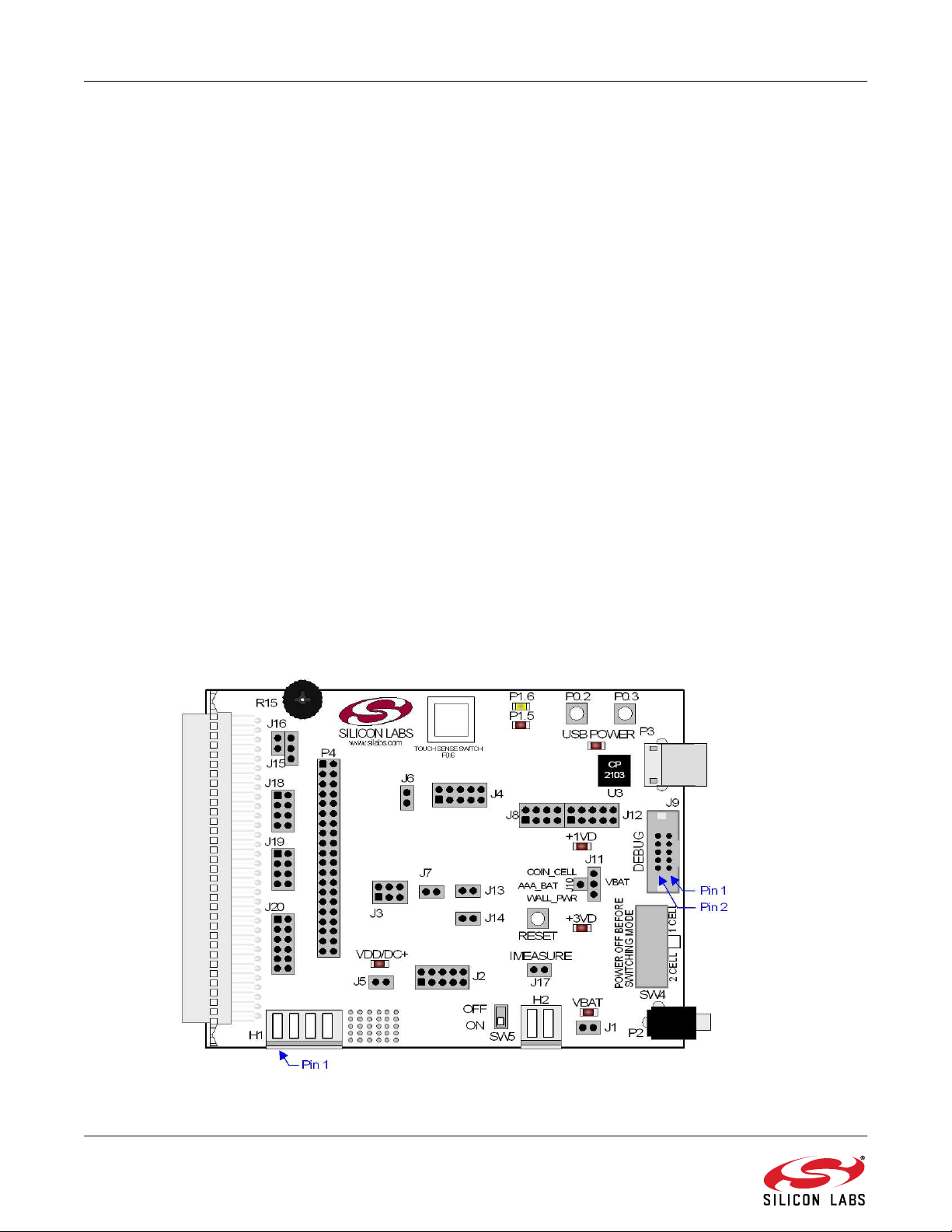
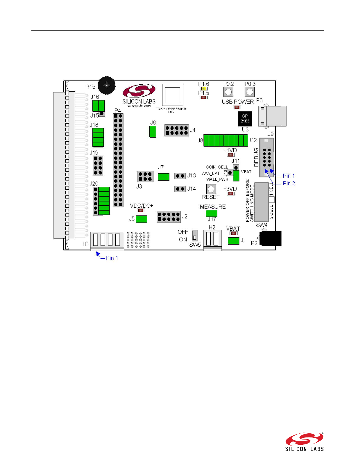
10. Motherboard
The Si1000 and Si1010 Development Kit includes a motherboard that enables evaluation and preliminary software
development. Numerous input/output (I/O) connections are provided to facilitate prototyping using the target board.
Refer to Figure 8 for the locations of the various I/O connectors. Figure 10 on page 14 shows the factory default
shorting block positions.
P1 Expansion connector (96-pin)
P2 Power connector (accepts input from 7 to 15 VDC unregulated power adapter)
P3 USB connector (connects to PC for serial communication)
J1 Enable/Disable VBAT Power LED
J2, J3, J4 Port I/O headers (provide access to Port I/O pins)
J5 Enable/Disable VDD/DC+ Power LED
J6 Provides an easily accessible ground clip
J7 Connects pin P0.7 (IREF0 Output) to resistor R14 and capacitor C19
J8 Connects P0.2 and P0.3 to switches and P1.5 and P1.6 to LEDs
J9 DEBUG connector for Debug Adapter interface
J10, J11 Selects the power supply source (Wall Power, AAA Battery, or Coin Cell)
J12 Connects Port I/O to UART0 interface
J13 Connects external VREF capacitor to the P0.0/VREF
J14 Connects the PCB ground plane to P0.1/AGND
J15 Connects negative potentiometer (R14) terminal to pin P1.4 or to GND
J16 Connects the potentiometer (R14) wiper to P0.6/CNVSTR
J17 Creates an open in the power supply path to allow supply current measurement
J18,J19 Connects signals on P1 to the appropriate GPIO. Short J18 for Si100x and J19 for Si101x.
J20 Connects signals on J18/J19 to the EEPROM accessible through P4.
H1 Analog I/O terminal block
H2 Provides terminal block access to the input and output nodes of J17
SW4 Switches the device between One-Cell (0.9–1.8 V supply) or Two-Cell (1.8–3.6 V) mode
SW5 Turns power to the MCU on or off
Figure 8. Si1000 Motherboard
12 Rev. 0.1
Page 13
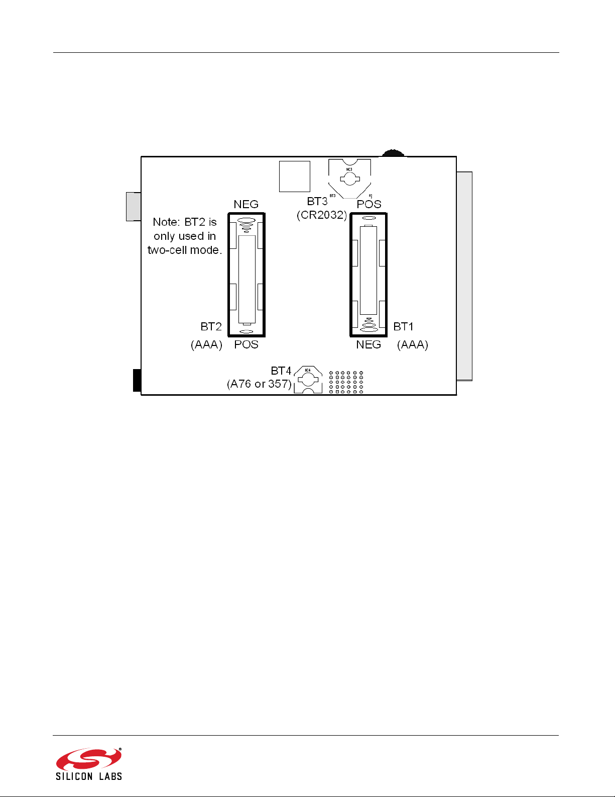
The following items are located on the bottom side of the board. See Figure 9.
BT1 Battery Holder for 1.5 V AAA. Use for one-cell or two-cell mode.
BT2 Battery Holder for 1.5 V AAA. Use for two-cell mode only.
BT3 Battery Holder for 3 V Coin Cell (CR2032).
BT4 Battery Holder for 1.5 V Button Cell (A76 or 357).
Si10xx-DK
Figure 9. Bottom of Si1000 Motherboard
Rev. 0.1 13
Page 14
Si10xx-DK
10.1. Motherboard Shorting Blocks: Factory Defaults
The Si1000 motherboard comes from the factory with pre-installed shorting blocks on many headers. Figure 10
shows the positions of the factory default shorting blocks.
Figure 10. Si1000 Motherboard Shorting Blocks: Factory Defaults
14 Rev. 0.1
Page 15

Si10xx-DK
10.2. Target Board Power Options and Current Measurement
The Si10xx Target Board supports three power options, selectable by the three-way header (J10/J11). The power
options vary based on the configuration (one-cell or two-cell mode) selected by SW4. Power to the MCU may be
switched on/off using the power switch (SW5). Important Note: The power switch (SW5) must be in the OFF
position prior to switching between one-cell and two-cell mode using SW4. The power options are described
in the paragraphs below.
10.2.1. Wall Power
When the J10/J11 three-way header is set to WALL_PWR, the Si10xx Motherboard may be powered from the
following power sources:
9 VDC power using the ac to dc power adapter (P2)
5 VDC USB VBUS power from PC via the USB Debug Adapter (J9)
5 VDC USB VBUS power from PC via the CP2103 USB connector (P3)
All the three power sources are ORed together using reverse-biased diodes (D1, D2, D3), eliminating the need for
headers to choose between the sources. The target board will operate as long as any one of the power sources is
present. The ORed power is regulated to a 3.3 V dc voltage using a LDO regulator (U2). The output of the regulator
powers the +3 VD net on the target board.
If SW4 is configured to select two-cell mode, the VBAT supply net on the target board is powered directly from the
+3 VD net. If SW4 is configured to select one-cell mode, the VBAT supply net is powered directly from the +1 VD.
This power supply net takes +3 VD and passes it through a 1.65 V LDO. The LDO’s output voltage is variable and
can be set by changing the value of resistor R32.
10.2.2. AAA Battery
When the J10/J11 three-way header is set to AAA_BAT, the Si10xx Target Board may be powered from a single
AAA battery inserted in BT1 or from the series combination of the AAA batteries inserted in BT1 and BT2. A single
battery is selected when SW4 is configured to one-cell mode. The two AAA batteries configured in series to provide
a voltage of ~3 V are selected when SW4 is configured to two-cell mode.
10.2.3. Coin Cell Battery
When the J10/J11 three-way header is set to COIN_CELL, the Si10xx Target Board may be powered from a single
1.5 V Alkaline (A76) or Silver Oxide (357) button cell inserted in BT4 or from a single 3 V Lithium (CR2032) coin
cell inserted in BT3. The button cell (BT4) is selected when SW4 is configured to one-cell mode, and the coin cell
(BT3) is selected when SW4 is configured to two-cell mode.
10.2.4. Measuring Current
The header (J17) and terminal block (H2) provide a way to measure the total supply current flowing from the power
supply source to the MCU. The measured current does not include any current from the VBAT LED (DS2), the
address latch (U4) or the quiescent current from the power supply; however, it does include the current used by
any LEDs powered from the VDD/DC+ supply net or sourced through a GPIO pin. See the target board schematic
in Figure 11 through Figure 13 for additional information.
Rev. 0.1 15
Page 16

Si10xx-DK
10.3. System Clock Sources
10.3.1. Internal Oscillators
The Si10xx or Si1010 device installed on the daughtercard features a factory calibrated programmable highfrequency internal oscillator (24.5 MHz base frequency, ±2%) and a low power internal oscillator (20 MHz ±10%).
After each reset, the low power oscillator divided by 8 results in a default system clock frequency of 2.5 MHz
(±10%). The selected system clock and the system clock divider may be configured by software for operation at
other frequencies. For low-frequency operation, the Si10xx and Si1010 features a smaRTClock real time clock. A
32.768 kHz watch crystal (Y2) is included on the daughtercard. If you wish to operate the Si10xx device at a
frequency not available with the internal oscillators, an external crystal may be used. Refer to the Si100x or Si101x
data sheet for more information on configuring the system clock source.
10.3.2. External Oscillator Options
The daughtercards are designed to facilitate the installation of an external crystal (Y1). Install a 10 M resistor at
R9 and install capacitors at C20 and C21 using values appropriate for the crystal you select. If you wish to operate
the external oscillator in capacitor or RC mode, options to install a capacitor or an RC network are also available on
the target board. Populate C21 for capacitor mode, and populate R16 and C21 for RC mode. Refer to the Si100xSi101x data sheet for more information on the use of external oscillators.
10.4. Port I/O Headers (J2, J3, J4, J6)
Access to all Port I/O on the Si10xx is provided through the headers J2, J3, and J4. The header J6 provides access
to the ground plane for easy clipping of oscilloscope probes.
16 Rev. 0.1
Page 17

Si10xx-DK
10.5. Switches and LEDs
Three push-button switches are provided on the target board. Switch SW1 is connected to the reset pin of the
MCU. Pressing SW1 puts the device into its hardware-reset state. Switches SW2 and SW3 are connected to the
MCU’s general purpose I/O (GPIO) pins through headers. Pressing SW2 or SW3 generates a logic low signal on
the port pin. Remove the shorting block from the header (J8) to disconnect the switches from the port pins. The
port pin signal is also routed to pins on the J2 and P1 I/O connectors. See Table 1 for the port pins and headers
corresponding to each switch.
Two touch sensitive (contactless) switches are provided on the target board. The operation of these switches
require appropriate firmware running on the Si10xx MCU that can sense the state of the switch.
Five power LEDs are provided on the target board to serve as indicators. Each of the two regulators has a red LED
used to indicate the presence of power at the output of the regulator. A red USB Power LED turns on when a USB
cable is plugged into the USB connector P3. One power LED is also added to each of the two primary supply nets
powering the MCU (VDD/DC+ and VBAT). The LEDs connected to the supply nets may be disabled by removing
the shorting blocks from J1 and J5.
Two LEDs are connected to GPIO pins P1.5 and P1.6 for use by application software. See Table 1 for the port pins
and headers corresponding to each LED.
A potentiometer (R15) is also provided on the target board for generating analog signals. Place a shorting block on
J16 to connect the wiper to P0.6/CNVSTR. The header J15 allows the negative terminal of the potentiometer to be
tied to GND or to P2.7. When tied to GND, the potentiometer is always enabled and will draw a measurable
amount of supply current. When tied to P2.7, it only draws current when P2.7 is driving a logic 0 and draws no
current when P2.7 is driving a logic 1.
Table 1. Target Board I/O Descriptions
Description I/O Header(s)
SW1 Reset none
SW2 P0.2 J8[5–6]
SW3 P0.3 J8[7–8]
P0.6 (Touch Sense Switch) P0.6 none
Red LED (P1.5) P1.5 J8[1–2]
Yellow LED (P1.6) P1.6 J8[3–4]
Red LED (VDD/DC+) VDD/DC+ Supply Net J5
Red LED (VBAT) VBAT Supply Net J1
Red LED (USB Power) USB VBUS none
Red LED (+1 VD Power) +1 VD Regulator Output none
Red LED (+3 VD Power) +3 VD Regulator Output none
Potentiometer (R15) P0.6/P2.7 J15, J16
Rev. 0.1 17
Page 18

Si10xx-DK
10.6. Expansion I/O Connector (P1)
The 96-pin Expansion I/O connector P1 provides access to all signal pins of the Si10xx device (except the C2
debug interface signals). In addition, power supply and ground pins are included. A small through-hole prototyping
area is also provided. See Table 2 for a list of pin descriptions for P1.
Table 2. P1 Pin Descriptions
Row A
Pin #
1 +3 VD 1 GND 1 nc
2 nc 2 nc 2 nc
3 nc 3 nc 3 nc
4 nc 4 nc 4 nc
5 nc 5 nc 5 nc
6 nc 6 nc 6 nc
7 nc 7 nc 7 nc
8 nc 8 nc 8 nc
9 GPIO_2 9 GPIO_1 9 GPIO_0
10 nc 10
11
12 P0.2H 12
13 P2.1 13 nc 13 nc
14
15 MISO/SCL 15 SCK/SDA 15 nc
16 nc 16 nc 16 nc
17
18 nc 18 nc 18 nc
19 nc 19 nc 19 nc
20 nc 20 nc 20 nc
21 nc 21 nc 21 nc
22
23 nc 23 nc 23 nc
24 nc 24 nc 24 nc
25 nc 25 GND 25 nc
26 GND 26 nc 26 nc
27 nc 27 nc 27 nc
28 nc 28 VDD/DC+ 28 VBAT
29 nc 29 nc 29 nc
30 nc 30 nc 30 nc
31 nc 31 nc 31 nc
32 nc 32 GND 32 nc
Description
P0.5/RX
CLK 14 NSS/PWR 14 MOSI
nc
nc
Row B
Pin #
11
17
22
Description
P0.1/AGND
P0.4/TX
P0.7/IREF0
nc
nc
Row C
Pin #
10
11 P0.3H
12
17
22
Description
P0.6/CNVSTR
P0.0/VREF
nc
nc
18 Rev. 0.1
Page 19

Si10xx-DK
10.7. Target Board DEBUG Interface (J9)
The
DEBUG
Adapter or the USB Debug Adapter to the target board for in-circuit debugging and Flash programming. Table 3
shows the
10.8. Serial Interface (J12)
A USB-to-UART bridge circuit (U3) and USB connector (P3) are provided on the target board to facilitate serial
connections to UART0 of the Si10xx. The Silicon Labs CP2103 (U3) USB-to-UART bridge provides data
connectivity between the Si10xx and the PC via a USB port. The VIO power supply and TX, RX, RTS and CTS
signals of UART0 may be connected to the CP2103 by installing shorting blocks on header J12. The shorting block
positions for connecting each of these signals to the CP2103 are listed in Table 4. To use this interface, the USBto-UART device drivers should be installed as described in Section 3.2. "CP210x USB to UART VCP Driver
Installation‚" on page 2.
connector J9 provides access to the
DEBUG
pin definitions.
Table 3. DEBUG Connector Pin Descriptions
Pin # Description
1 +3 VD (+3.3 VDC)
2, 3, 9 GND (Ground)
4 P2.7/C2D
5
6 P2.7
7 RST/C2CK
8 Not Connected
10 USB Power (+5 VDC from J9)
DEBUG
RST (Reset)
(C2) pins of the Si10xx. It is used to connect the Serial
Table 4. Serial Interface Header (J12) Description
Header Pins UART0 Pin Description
J12[9–10] CP2103_VIO (VDD/DC+)
J12[7–8] TX_MCU (P0.5)
J12[5–6] RX_MCU (P0.4)
J12[3–4] RTS (P0.6)
J12[1–2] CTS (P0.7)
10.9. Analog I/O (H1)
Several of the Si10xx target device’s port pins are connected to the H1 terminal block. Refer to Table 5 for the H1
terminal block connections.
Table 5. H1 Terminal Block Pin Descriptions
Pin # Description
1 P0.6/CNVSTR
2 P0.7/IREF0
3 GND (Ground)
4 P0.0/V
(Voltage Reference)
REF
Rev. 0.1 19
Page 20

Si10xx-DK
10.10. IREF Connector (J7)
The Si1000 Motherboard also features a current-to-voltage 1 k load resistor that may be connected to the current
reference (IREF0) output that can be enabled on port pin (P0.7). Install a shorting block on J7 to connect port pin
P0.7 of the target device to the load resistor. If enabled by software, the IREF0 signal is then routed to the J2[8]
and H1[2] connectors.
10.11. VREF and AGND Connector (J13, J14)
The Si1000 Motherboard also features 4.7 μF capacitor in parallel with a 0.1 μF that can be connected to P0.0/
VREF when using the Precision Voltage Reference. The capacitors are connected to P0.0/VREF when a shorting
block is installed on J13. Using the Precision Voltage Reference is optional since Si10xx devices have an on-chip
High-Speed Voltage Reference.
The shorting block J14 allows P0.1/AGND to be connected to ground. This provides a noise-free ground reference
to the analog-to-digital Converter. The use of this dedicated analog ground is optional.
10.12. C2 Pin Sharing
On the Si10xx, the debug pins C2CK and C2D are shared with the pins
board includes the resistors necessary to enable pin sharing which allow the RST and P2.7 pins to be used
normally while simultaneously debugging the device. See Application Note “AN124: Pin Sharing Techniques for the
C2 Interface” at www.silabs.com for more information regarding pin sharing.
RST and P2.7, respectively. The target
20 Rev. 0.1
Page 21

11. Schematics
Rev. 0.1 21
Figure 11. Si1000 Motherboard Schematic (1 of 3)
Si10xx-DK
Page 22

22 Rev. 0.1
Si10xx-DK
Figure 12. Si1000 Motherboard Schematic (2 of 3)
Page 23

Rev. 0.1 23
Figure 13. Si1000 Motherboard Schematic (3 of 3)
Si10xx-DK
Page 24

24 Rev. 0.1
EBID_MOSI,EBID_MISO,EBID_SCK,EBID_NSEL
P2.6
P2.7/C2D
NRST/C2CK
P0.0
GND
21
N.F.
32.768 kHz
C26
C27
SJ11
SJ12
SJ13
21
21
GPIO0
GPIO2
GPIO1
SDN
21
VDD_MCU
GND
Q4
P0.2
N.F.
N.F.
VDD_MCU
C21 C28
100pF 100nF
GND
100nF
100nF
GND
P0.3
SDN
21
SJ3
GND
1k
R18
VDD_MCU
12
34
56
78
910
GND
SJ4
21
VDD
R2
10k
SDN
R11
GND
C20
N.F.
TP4
J1
10 PIN, straith male
P2.2(P1.5)
P2.0(P0.7)
P2.3(P1.6)
R8
10k
P0.4
N.F.
P0.5
SJ9
21
P0.6
+5V
N.F.
(DCEN)
100k
(VBAT)
P2.4
R7
10k
P2.5
SJ6
21
P2.6
SJ5
21
(GND/DC)
GND
CS1
.2)
(P1
12
P0.7
(P1.0)
(
34
(P1.3)
56
78
P0.0
910
P0.1
11 12
13 14
P0.2
15 16
P2.1(P1.4)
17 18
19 20
21 22
P0.3
23 24
P1.5
25 26
27 28
29 30
31 32
33 34
P1.6
35 36
P1.7
37 38
P2.7/C2D
39 40
NRST/C2CK
CON40-0
P1.4)
VDD_RF
N.F.
100k
EBID_MOSI
EBID_MISO
EBID_SCK
EBID_NSEL
R12
TEST PINS
NIRQ
P0.0
P0.0
P0.1
P0.1
P0.2
P0.2
P0.3
P0.3
P0.4
P0.4
P0.5
P0.5
P0.6
P0.6
P0.7
P0.7
P1.5
P1.5
P1.6
P1.6
P1.7
P1.7
P2.0(P0.7)
P2.0
P2.1(P1.4)
P2.1
P2.2(P1.5)
P2.2
P2.3(P1.6)
P2.3
P2.4
P2.4
P2.5
P2.5
P2.6
P2.6
P2.7/C2D
P2.7/C2D
NRST/C2CK
NRST/C2CK
GND
GND2
GND
VDD2
VDD
VDD
L3
0R
(P1.1)
L4
VDD
0R
VDD_RF
GND
VDD_MCU
C25
1uF
GND
C24
1uF
+5V
EBID_NSEL
EBID_MOSI
EBID_SCK
**** Optional part is NOT MOUNTED.
ANT
GND
GND
LM2
8.2nH
GND
GND
+5V
+5V
R4R5
IC2
100kN.F.
3
1
5
6
7
GND
WP
CS
SI
SCK
HOLD
25AA080C
C
C2
CM2CM3
4.3pF4.3pF
56pF
84
VCC
2
EBID_MISO
SO
C23
Array
EEPROM
GND
100nF
GND
GPIO2
21
UPG2214TB6SM
SJ10
21
SJ8
GPIO1
Si4432 RevB1 switch matching
VC2
5
RF_IN
6
VC1
19.11.2009
915MHz
34
OUT2
2
GND
1
OUT1
IC4
VDD
C4
RDC
2.2uF
0R
GND
LM L0
CC1
56pF
GND
12nH
GND
GND
GND
GND
12nH
CM
3pF
CR2
6.8pF
LR
11nH
CR1
3.3pF
C0
33pF
CH
5.6pF
RH
50R
GND
C1C2C3
33pF100pF100nF
GNDGNDGND
LC
120nH
LH
5.6nH
30MHz
Q3
14
NC1
SDN
15
SDN
16
VDD_RF
17
TX
18
RXP
19
RXN
20
VR_IF
21
NC2
NC322GND223GPIO_024GPIO_125GPIO_226VDR27VDD_DIG28P0.7/IREF029P0.6/CNVSTR30P0.5/RX31P0.4/TX32P0.3/XTAL233P0.2/XTAL134P0.1/AGND
EP_UC
P$1
GND GNDGND
32.768kHz
P1.7
P1.6
P1.5
NIRQ
10
11
12
13
XIN
NIRQ
XOUT
C16
C17
1uF
100pF
Q1
P2.4
P2.5
P2.0(P0.7)
P2.3(P1.6)
P2.1(P1.4)
P2.2(P1.5)
1
P2.52P2.43P2.34P2.25P2.16P2.07P1.78P1.69P1.5
XTAL3
42
XTAL4
41
P2.6
40
P2.7/C2D
39
NRST/C2CK
38
VDD_MCU
37
GND4
36
P0.0/VREF
EP_RF
35
P$2
P0.7
P0.6
P0.5
P0.4
VDD_RF
C11
100nF
GNDGNDGND
SJ1
P0.1
P0.3/XTAL2
P0.2/XTAL1
VDD_MCU
Q5
R20
R19
N.F.
N.F.
1k
1k
Si10xx-DK
Figure 14. Si1000 Daughtercard Schematic
Page 25

NOTES:
Si10xx-DK
Rev. 0.1 25
Page 26

Smart.
Connected.
Energy-Friendly.
Products
www.silabs.com/products
Disclaimer
Silicon Laboratories intends to provide customers with the latest, accurate, and in-depth documentation of all peripherals and modules available for system and software implementers using
or intending to use the Silicon Laboratories products. Characterization data, available modules and peripherals, memory sizes and memory addresses refer to each specific device, and
"Typical" parameters provided can and do vary in different applications. Application examples described herein are for illustrative purposes only. Silicon Laboratories reserves the right to
make changes without further notice and limitation to product information, specifications, and descriptions herein, and does not give warranties as to the accuracy or completeness of the
included information. Silicon Laboratories shall have no liability for the consequences of use of the information supplied herein. This document does not imply or express copyright licenses
granted hereunder to design or fabricate any integrated circuits. The products are not designed or authorized to be used within any Life Support System without the specific written consent
of Silicon Laboratories. A "Life Support System" is any product or system intended to support or sustain life and/or health, which, if it fails, can be reasonably expected to result in significant
personal injury or death. Silicon Laboratories products are not designed or authorized for military applications. Silicon Laboratories products shall under no circumstances be used in
weapons of mass destruction including (but not limited to) nuclear, biological or chemical weapons, or missiles capable of delivering such weapons.
Trademark Information
Silicon Laboratories Inc.® , Silicon Laboratories®, Silicon Labs®, SiLabs® and the Silicon Labs logo®, Bluegiga®, Bluegiga Logo®, Clockbuilder®, CMEMS®, DSPLL®, EFM®, EFM32®,
EFR, Ember®, Energy Micro, Energy Micro logo and combinations thereof, "the world’s most energy friendly microcontrollers", Ember®, EZLink®, EZRadio®, EZRadioPRO®, Gecko®,
ISOmodem®, Precision32®, ProSLIC®, Simplicity Studio®, SiPHY®, Telegesis, the Telegesis Logo®, USBXpress® and others are trademarks or registered trademarks of Silicon Laboratories Inc. ARM, CORTEX, Cortex-M3 and THUMB are trademarks or registered trademarks of ARM Holdings. Keil is a registered trademark of ARM Limited. All other products or brand
names mentioned herein are trademarks of their respective holders.
Silicon Laboratories Inc.
400 West Cesar Chavez
Austin, TX 78701
USA
Quality
www.silabs.com/quality
Support and Community
community.silabs.com
http://www.silabs.com
Page 27

 Loading...