

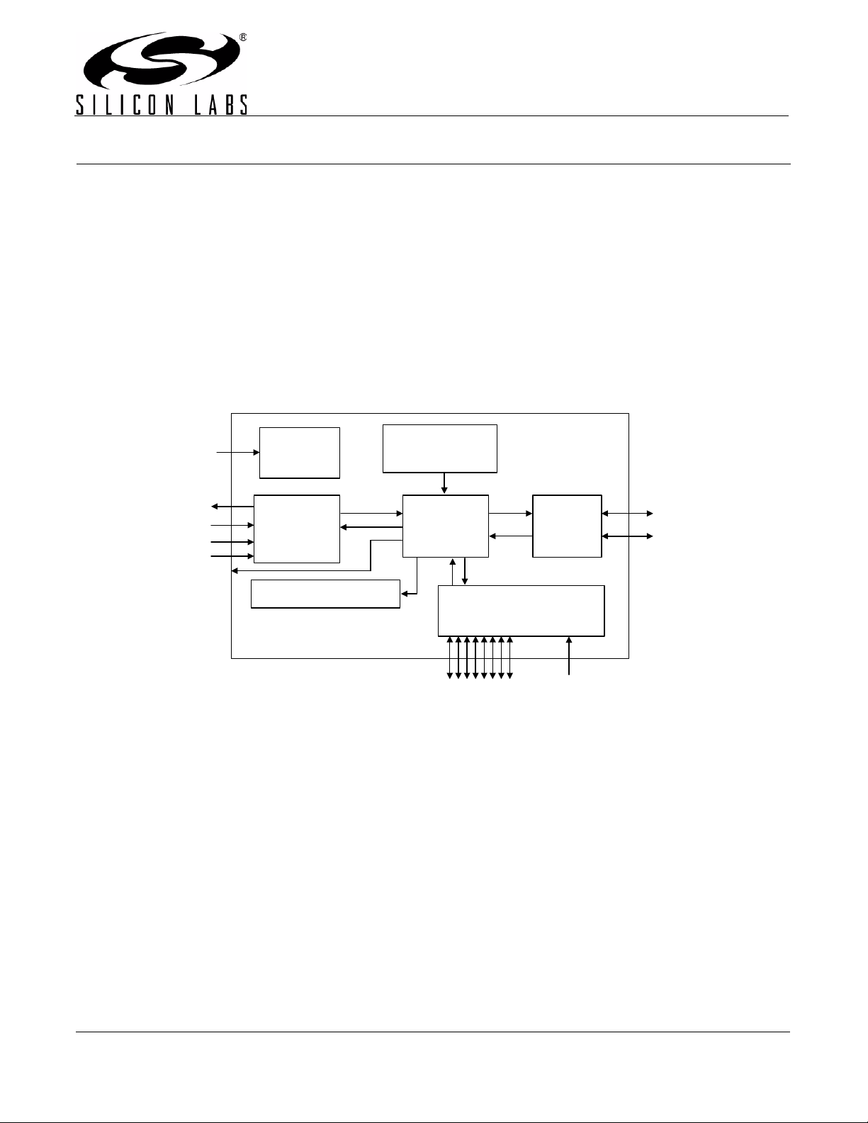
CP2120
SPI TO I2C BRIDGE AND GPIO PORT EXPANDER
Single Chip SPI to I2C Transfer
Integrated clock; no external clock required
On-Chip Voltage Monitor
Slave Serial Peripheral Interface (SPI)
Up to 1.0 Mbit/s Transfers
Configurable to Least Significant Bit or Most Significant
Bit first byte transfers
I2C Master Interface
Operates at configurable rates up to 400 kHz
255 RX and TX Data Buffers
Voltage
Monitor
MISO
MOSI
SCK
CS
SPI
Interface
Internal Registers
Input and Output Port Pins
8 Pins Configurable as Push-Pull or Open-Drain
1 Pin Configurable as an edge-triggered interrupt
source
All pins 5 V Tolerant
INT active low interrupt pin
Supply Voltage of 2.7 V to 3.6 V
Typical operating current: 6.4 mA
Package
Pb-free 20-pin QFN
Internal
Oscillator
2
C
Controller
I
Interface
Port Controller
SDA
SCL
Eight I/O Pins
Edge-Triggered
Interrupt Source
Figure 1. Block Diagram
Rev. 0.3 5/07 Copyright © 2007 by Silicon Laboratories CP2120
This information applies to a product under development. Its characteristics and specifications are subject to change without notice.

CP2120
2 Rev. 0.3

CP2120
TABLE OF CONTENTS
Section Page
1. System Overview . . . . . . . . . . . . . . . . . . . . . . . . . . . . . . . . . . . . . . . . . . . . . . . . . . . . . . . . .4
2. Absolute Maximum Ratings . . . . . . . . . . . . . . . . . . . . . . . . . . . . . . . . . . . . . . . . . . . . . . . .4
3. Global DC Electrical Characteristics . . . . . . . . . . . . . . . . . . . . . . . . . . . . . . . . . . . . . . . . .4
4. Pinout And Package Definition . . . . . . . . . . . . . . . . . . . . . . . . . . . . . . . . . . . . . . . . . . . . . .5
4.1. Pin Out Chart . . . . . . . . . . . . . . . . . . . . . . . . . . . . . . . . . . . . . . . . . . . . . . . . . . . . . . .5
4.2. QFN-20 Pinout Diagram (Top View) . . . . . . . . . . . . . . . . . . . . . . . . . . . . . . . . . . . . . . 6
4.3. QFN-20 Pinout Diagram (Bottom View) . . . . . . . . . . . . . . . . . . . . . . . . . . . . . . . . . . .7
4.4. QFN-20 Solder Paste Recommendations . . . . . . . . . . . . . . . . . . . . . . . . . . . . . . . . . .8
5. SPI Slave Bus . . . . . . . . . . . . . . . . . . . . . . . . . . . . . . . . . . . . . . . . . . . . . . . . . . . . . . . . . . . .9
5.1. Command Set . . . . . . . . . . . . . . . . . . . . . . . . . . . . . . . . . . . . . . . . . . . . . . . . . . . . . . 10
5.2. Internal Registers . . . . . . . . . . . . . . . . . . . . . . . . . . . . . . . . . . . . . . . . . . . . . . . . . . .10
5.3. SPI Byte Orientation . . . . . . . . . . . . . . . . . . . . . . . . . . . . . . . . . . . . . . . . . . . . . . . . . 11
5.4. SPI Timing Diagrams . . . . . . . . . . . . . . . . . . . . . . . . . . . . . . . . . . . . . . . . . . . . . . . . 11
2
5.5. I
6. I2C Serial Interface . . . . . . . . . . . . . . . . . . . . . . . . . . . . . . . . . . . . . . . . . . . . . . . . . . . . . . .13
6.1. Determining Pull-Up Register Values . . . . . . . . . . . . . . . . . . . . . . . . . . . . . . . . . . . . 13
6.2. I2C Internal Registers . . . . . . . . . . . . . . . . . . . . . . . . . . . . . . . . . . . . . . . . . . . . . . . . 13
6.3. I2C Status . . . . . . . . . . . . . . . . . . . . . . . . . . . . . . . . . . . . . . . . . . . . . . . . . . . . . . . . .15
6.4. I2C Receive Buffer Size . . . . . . . . . . . . . . . . . . . . . . . . . . . . . . . . . . . . . . . . . . . . . .17
6.5. I2C Commands . . . . . . . . . . . . . . . . . . . . . . . . . . . . . . . . . . . . . . . . . . . . . . . . . . . . .17
7. Port I/O . . . . . . . . . . . . . . . . . . . . . . . . . . . . . . . . . . . . . . . . . . . . . . . . . . . . . . . . . . . . . . . .19
8. CP2120 Revision Number . . . . . . . . . . . . . . . . . . . . . . . . . . . . . . . . . . . . . . . . . . . . . . . . .22
Document Change List . . . . . . . . . . . . . . . . . . . . . . . . . . . . . . . . . . . . . . . . . . . . . . . . . . . . .23
Contact Information . . . . . . . . . . . . . . . . . . . . . . . . . . . . . . . . . . . . . . . . . . . . . . . . . . . . . . . .24
C Activity During SPI Transactions . . . . . . . . . . . . . . . . . . . . . . . . . . . . . . . . . . . . . 12
Rev. 0.3 3
CP2120
1. System Overview
The CP2120 is a highly-integrated SPI-to-I2C Bridge Controller with an SPI interface that provides a simple and
reliable method for communicating with I
(SPI), a serial I
configurable as an edge-triggered interrupt source in a compact 4x4 package. No external components other than
pull-up resisters on the I
a command set that governs all CP2120 configuration and operation.
2
C interface, 256 byte data buffers, an internal oscillator, eight input/output port pins, and one pin
2
C pins are required. The SPI Master controls the CP2120 across the SPI interface using
2
C devices. The CP2120 includes a 4-wire serial peripheral interface
2. Absolute Maximum Ratings
Table 1. Absolute Maximum Ratings
Parameter Conditions Min Typ Max Units
Ambient temperature under bias –55 — 125 °C
Storage Temperature –65 — 150 °C
Voltage on any Port I/O Pin or RST
to GND
Voltage on V
Maximum Total current through V
Maximum output current sunk by RST
Port pin
with respect to GND –0.3 — 4.2 V
DD
with respect
or GND — — 500 mA
DD
or any
–0.3 — 5.8 V
——100mA
Note: Stresses above the absolute maximum ratings may cause permanent device damage. This is a stress rating only, and
functional operation of the devices at any conditions equal to or greater than those indicated in the operational listings
of this specification are not implied. Exposure to maximum rating conditions for extended periods may affect device
reliability.
3. Global DC Electrical Characteristics
Table 2. Global Electrical Characteristics
–40 to +85 °C, 25 MHz system clock unless otherwise specified.
Parameter Conditions Min Typ Max Units
Digital Supply Voltage V
Digital Supply Current V
Specified Operating
Temperature Range
=2.7V — TBD — mA
DD
RST
–40 — +85 °C
3.0 3.6 V
4 Rev. 0.3
4. Pinout And Package Definition
4.1. Pin Out Chart
Name Pin # Type Description
CP2120
V
DD
GND 2 Ground
RST 4 Digital I/O Device Reset. Open-drain output of internal POR or VDD monitor. An
SCLK 1 Digital In SPI Clock Input
MISO 20 Digital Out SPI Slave Output
MOSI 19 Digital In SPI Slave Input
CS 18 Digital In SPI Slave Select
SDA 17 Digital I/O I
SCL 16 Digital I/O I
GPIO 0 5 Digital I/O General Purpose Configurable Digital Input/Output
GPIO 1 12 Digital I/O General Purpose Configurable Digital Input/Output
GPIO 2 11 Digital I/O General Purpose Configurable Digital Input/Output
GPIO 3 10 Digital I/O General Purpose Configurable Digital Input/Output
GPIO 4 9 Digital I/O General Purpose Configurable Digital Input/Output
3 Power Supply Pin
external source can initiate a system reset by driving this pin low for at
least 15 µs.
2
C Data Input/Output
2
C Clock Input/Output
GPIO 5 8 Digital I/O General Purpose Configurable Digital Input/Output
GPIO 6 7 Digital I/O General Purpose Configurable Digital Input/Output
GPIO 7 6 Digital I/O General Purpose Configurable Digital Input/Output
EINT 13 Digital I/O Edge-Triggered Interrupt Source
INT 14 Digital Out CP2120 Interrupt Indicator
NC 15 Digital Out Not connected, leave floating
Rev. 0.3 5
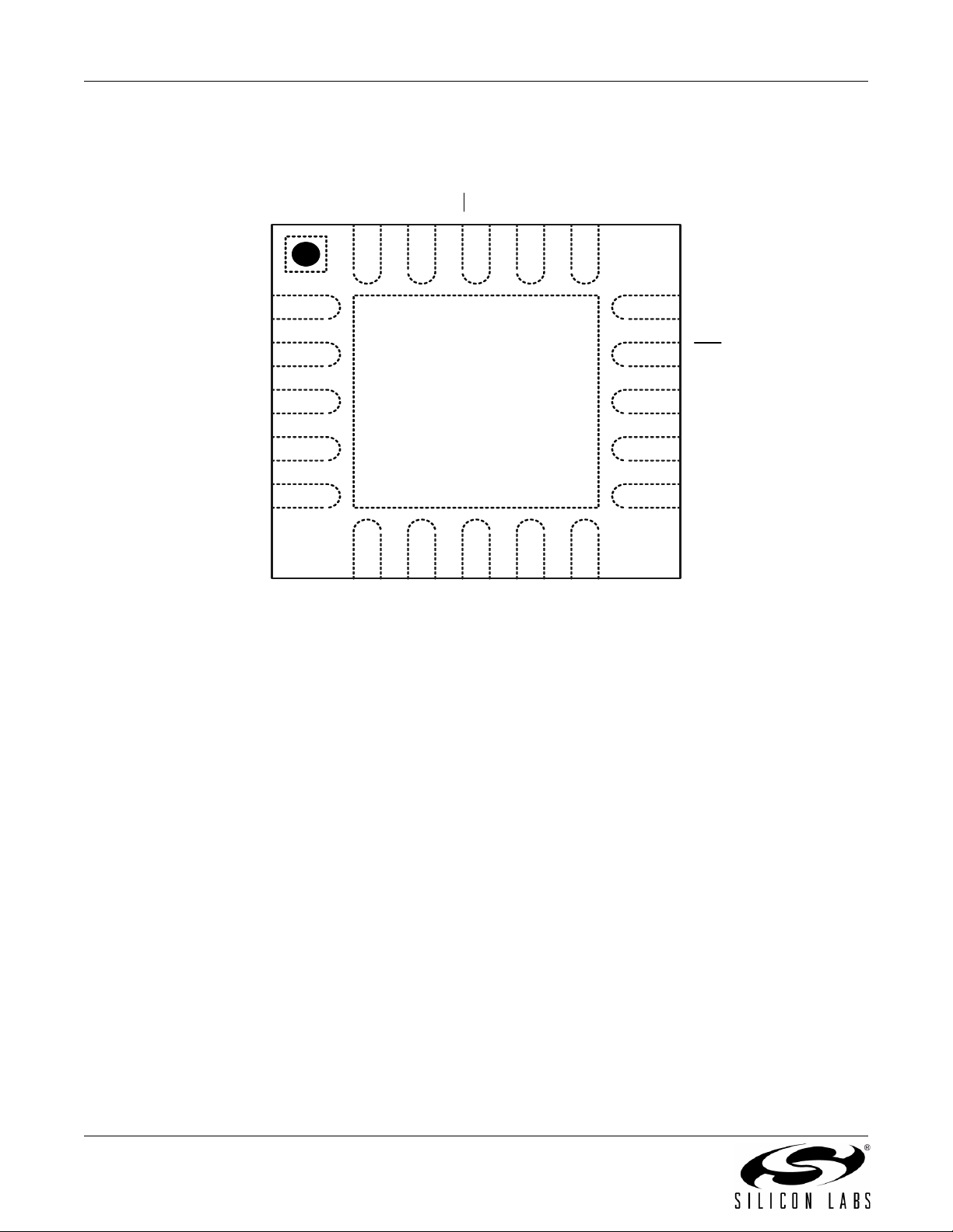
CP2120
4.2. QFN-20 Pinout Diagram (Top View)
SCLK
GND
VDD
/RST
GPIO 0
MISO
20
1
2
3
4
5
6
GPIO 7
MOSI
19
7
GPIO 6
CS
18
CP2120
GND
8
GPIO 5
SDA
17
9
GPIO 4
SCL
16
10
GPIO 3
15
14
13
12
11
NC
INT
EINT
GPIO 1
GPIO 2
6 Rev. 0.3
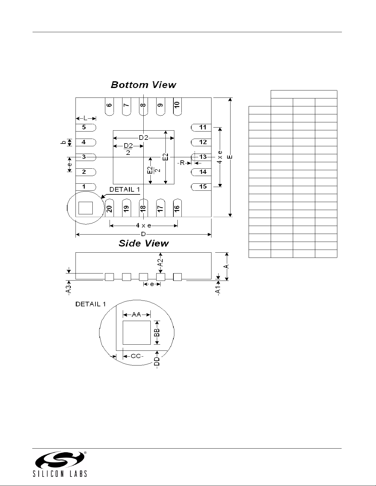
4.3. QFN-20 Pinout Diagram (Bottom View)
CP2120
Table 4.1. QFN-20
Package Dimensions
MM
MIN TYP MAX
A 0.80 0.90 1.00
A1 0 0.02 0.05
A2 0 0.65 1.00
A3 — 0.25 —
b 0.18 0.23 0.30
D—4.00—
D2 2.00 2.15 2.25
E—4.00—
E2 2.00 2.15 2.25
e—0.5—
L 0.45 0.55 0.65
N—20—
ND — 5 —
NE — 5 —
R0.09— —
AA — 0.435 —
BB — 0.435 —
CC — 0.18 —
DD — 0.18 —
Rev. 0.3 7
CP2120
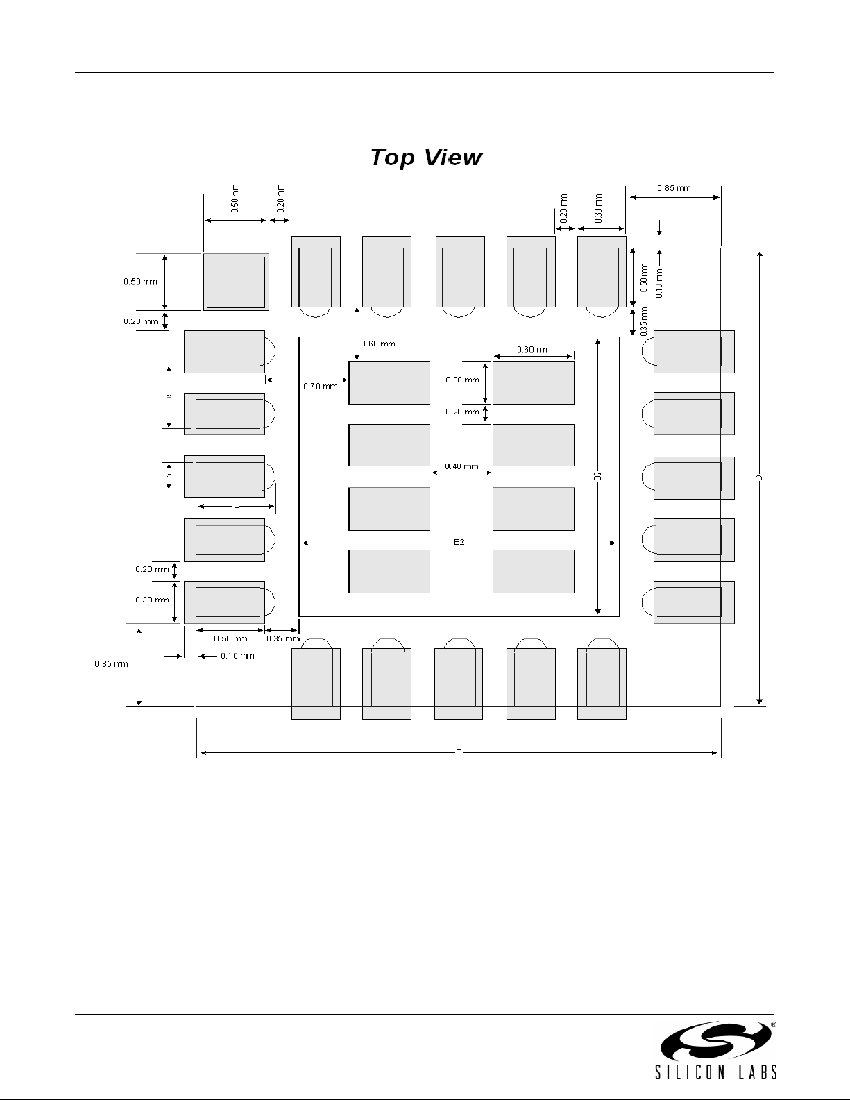
4.4. QFN-20 Solder Paste Recommendations
8 Rev. 0.3

CP2120
5. SPI Slave Bus
The CP2120 provides a four-wire slave SPI interface. The CP2120's SPI Bus activates whenever the SPI Master
pulls the NSS pin low. The master can then clock data into the CP2120 through the Master-Out-Slave-In (MOSI)
pin and receive data from the CP2120 through the Master-In-Slave-Out (MISO) pin. The SPI Master provides the
SPI with a clock source. Figure 2 shows typical connections for an SPI bus.
SPI Master
MISO
MOSI
SPICLK
CS
Figure 2. SPI Bus Typical Connections
SCLK should be held high when idle. Figure 3 shows a CP2120 data transfer on the SPI Bus. If the CP2120 is the
only slave device on the SPI bus, the NSS pin can be tied low.
SCK
MOSI
MISO
MSB
MSB Bit 6
Bit 6
Bit 5 Bit 4
Bit 5 Bit 4
SCLK
CS
Bit 3 Bit 2
Bit 3 Bit 2
CP2120
Bit 1
Bit 1
Bit 0
Bit 0
NSS
Figure 3. Slave Mode Data/Clock Timing
Rev. 0.3 9

CP2120
5.1. Command Set
An SPI Master controls the CP2120 by sending commands across the SPI bus. Some commands initiate I2C
transactions, while other commands modify or monitor CP2120 operation and events.
5.2. Internal Registers
The CP2120 maintains a set of internal registers that can be modified to configure general purpose port I/O and I2C
operation and can be read to obtain device status. Commands reading to and writing from the internal registers can
be issued at any time, even while an I
Table 3 shows a list of all internal registers.
2
C transaction is in progress, as they do not initiate any I2C bus transactions.
Table 3. Internal Register Addresses
Internal Register Address Section
IOCONFIG 0x00 7.
IOSTATE 0x01 7.
I2CCLOCK 0x02 6.1
I2CTO 0x03 6.1
I2CSTAT 0x04 6.2
I2CADR 0x05 6.1
RXBUFF 0x06 6.3
IOCONFIG2 0x07 7.
EDGEINT 0x08 7.
I2CTO2 0x09 6.1
5.2.1. Write to Internal Register
SPI Master
A Write to Internal Register command updates the value of one of the CP2120's Internal Registers. A Write to
Internal Register command begins with the command byte, 0x20, followed by the internal register address,
followed by the new value of the internal register. Only one register can be accessed per Write to Internal Register
command.
0x20
COMMAND
REGISTER
X
DATA BYTE
10 Rev. 0.3

5.2.2. Read From Internal Register
CP2120
SPI Master
CP2120
COMMAND
0x21
REGISTER
Address
Don’t Care
REGISTER
DATA
A Read from Internal Register command retrieves the current value of one of the CP2120's internal registers. The
command begins with the command byte, 0x21, followed by the internal register address. This byte is followed by
the transmission of a "don't care" byte, which can be of any value and is ignored by the CP2120. After the "don't
care" byte, the internal register value is transmitted across the MISO line.
5.3. SPI Byte Orientation
The SPI Configuration command configures the bit orientation of transfers across the SPI bus to one of two states.
If SPI transmits most-significant-bit first, bit 7 is transmitted first. If SPI transmits least-significant-bit first, bit 0 is
transmitted first.
5.3.1. SPI Configuration
SPI Master
COMMAND
0x18
CONFIGURATION
The command begins with the command byte (0x18), followed by SPI Configuration byte, which should equal one
of the values shown in the following table. Any values other than those listed in the table are ignored.
Byte Value Configuration
SPI
5.4. SPI Timing Diagrams
NSS
T
SE
SCK*
MOSI
T
SEZ
MISO
0x81 Most Significant Bit First
0x42 Least Significant Bit First
T
CKL
T
CKH
T
SIS
T
SOH
T
SIH
Figure 4. SPI Slave Timing
T
SD
T
SLH
T
SDZ
Rev. 0.3 11

CP2120
Slave Mode Timing* (See Figure 4)
T
T
T
T
T
T
T
T
T
T
SE
SD
SEZ
SDZ
CKH
CKL
SIS
SIH
SOH
SLH
NSS Falling to First SCLK Edge
Last SCLK Edge to NSS Rising
NSS Falling to MISO Valid
NSS Rising to MISO High-Z
SCLK High Time
SCLK Low Time
MOSI Valid to SCLK Sample Edge
SCLK Sample Edge to MOSI Change
SCLK Shift Edge to MISO Change
Last SCLK Edge to MISO Change
(CKPHA = 1 ONLY)
Table 4. SPI Slave Timing Parameters
2xT
SYSCLK
2xT
SYSCLK
—4xT
—4xT
5xT
SYSCLK
5xT
SYSCLK
2xT
SYSCLK
2xT
SYSCLK
—4xT
6xT
SYSCLK
—ns
—ns
SYSCLK
SYSCLK
ns
ns
—ns
—ns
—ns
—ns
ns
ns
8xT
SYSCLK
SYSCLK
*Note: T
equals 24.5 MHz.
SYSCLK
5.5. I2C Activity During SPI Transactions
If the SPI Master attempts to transmit a command to the CP2120 while the I2C bus is inactive, the CP2120 will
disable its slave response. If an I
CP2120 will not ACK the address defined in the I2CADR Internal Register.
If the SPI Master attempts to transmit a command to the CP2120 while the CP2120 is acting as the Master on the
2
I
C bus, the CP2120 will suspend I2C bus activity until the SPI Master has completed transmission of the
command. For instance, if the SPI Master calls the Read Internal Register command while the CP2120 is in the
middle of an I
2
C transaction, that I2C transaction will stall until the CP2120 completely processes the Read Internal
Register command.
2
C Master device on the bus attempts to address the CP2120 during this time, the
12 Rev. 0.3

6. I2C Serial Interface
CP2120
The CP2120 provides an I2C interface able to transfer data at frequencies up to 400 kHz. During a transaction, the
CP2120, operating as the I
SDA pin to and from an I
typical I
2
C bus.
I²C-bus
2
C master, sources a data clock on the SCL pin as data travels across the bidirectional
2
C slave device. The I2C interface lines each require a pull-up resistor. Figure 5 shows a
V
DD
CP2120
R
pU
I²C-BUS Device
Figure 5. Typical I
R
pU
2
C Bus*
SDA
SCL
I²C-BUS DEVI CE
*Note: VDD is defined in Table 1, “Absolute Maximum Ratings,” on page 4. For Rpu values, please see “6.1.
Determining Pull-Up Register Values” .
6.1. Determining Pull-Up Register Values
Logic low to logic high transitions on the SCL and SDA pins, which are configured to open-drain output with
external pull-ups to VDD, take the form of an exponential curve with an RC time constant, where C equals the
capacitance of the bus and R equals the pull-up resistor value. I
required for a signal level to change from Vmin +0.15 V to Vmax-0.15 V. By solving the exponential equation using
a Vmin of 0 V and a Vmax of 3.3 V, the following equation can be used to find values for pull-up resistors:
Rise time = 3.04448 RC
Bus capacitance is governed by a number of factors, including signal trace length and capacitance introduced by
devices on the bus. 8 mm PCB signal traces on a two-layer board generally add 1 pF of capacitance per
centimeter of trace length. To determine the amount of capacitance introduced to the bus by I
those devices’ datasheets. The maximum capacitance allowed before the bus violates I
Rise time requirements vary depending on each connected I
frequency. The maximum rise time allowed by the I
2
C specification is 1000 ns.
2
C specification defines rise time as the time
2
2
C specification is 400 pF.
2
C device’s timing requirements and the SCL clock
C devices, consult
6.2. I2C Internal Registers
Features of the I2C interface are configured through the CP2120's Internal Registers. SCL clock frequency is set
by writing to the I2CCLK Internal Register. The frequency can be determined using the equation below. The I
frequency configured by the I2CCLOCK register is only an approximate frequency. Actual I
2
C frequencies can vary
due to conditions on the bus, such as a slave device extending the SCL low time.
2000
I2C Clock Frequency (kHz)
Equation 1. I
2
C Clock Frequency
Rev. 0.3 13
---------------------
=
2
I
CCLK
2
C

CP2120
Internal Register Definition 1. I2CCLOCK: I2C Clock Frequency Configuration
R/W R/W R/W R/W R/W R/W R/W R/W
I2CCK7 I2CCK6 I2CCK5 I2CCK4 I2CCK3 I2CCK2 I2CCK1 I2CCK0
Bit 7 Bit 6 Bit 5 Bit 4 Bit3 Bit 2 Bit 1 Bit 0
Internal Register Address: 0x02
Reset Value: 0xA0
2
Bit 7-0: I2CCK7-0: I
maximum register value = 255)
The transaction time-out counter, which terminates an I2C transaction after a set period of time has passed, can be
configured through the I2CTO Internal Register. If the time-out counter is not enabled, the CP2120 will make only
one attempt at executing an I
2
C transaction and abort if that transaction attempt fails.
Internal Register Definition 2. I2CTO: I2C Time Out
C Clock Frequency Configuration value (minimum register value = 5,
TO
Time-out Frequency
--------- -
128
Hz()=
Equation 2. CTO Time-Out Frequency
R/W R/W R/W R/W R/W R/W R/W R/W
TO6 TO5 TO4 TO3 TO2 TO1 TO0 TEN
Bit 7 Bit 6 Bit 5 Bit 4 Bit3 Bit 2 Bit 1 Bit 0
Internal Register Address: 0x03
Reset Value: 0x00
Bit 7-1: TO6-0: Time Out Value
Bit 0: TEN:Time Out Enable Bit.
0: Disable Timer.
1: Enable Timer.
The SPI Master can assign an I2C address to the CP2120 by writing to the I2CADR Internal Register. Setting this
address is not necessary for device operation. If set, the CP2120 will ACK this address when another I
on the bus attempts to communicate with it. The CP2120 will NACK all attempts at data transfer when responding
2
as an I
C slave.
2
C Master
Internal Register Definition 3. I2CADR: I2C Address
R/W R/W R/W R/W R/W R/W R/W R/W
I2CAD7 I2CAD6 I2CAD5 I2CAD4 I2CAD3 I2CAD2 I2CAD1 I2CAD0
Bit 7 Bit 6 Bit 5 Bit 4 Bit3 Bit 2 Bit 1 Bit 0
Internal Register Address: 0x05
Reset Value: 0x00
Bit 7-Bit 0: I2CAD7-0: I
Sets I2C bus address.
2
C Address
14 Rev. 0.3

CP2120
The SPI2I2C provides additional SMBus-related timers to enable I2C protocol compatibility. Setting the I2C Bus
Free Detect enables the device to poll the SMBus lines and determine when a transfer can begin. Setting the SCL
Low Time Out detect will cause an SMBus transaction to abort if the SCL line has been held low by a device for a
period of approximately 25 ms.
Internal Register Definition 4. I2CTO2: Additional I2C Time Outs
R/W R/W R/W R/W R/W R/W R/W R/W
Reserved Reserved Reserved Reserved Reserved Reserved FREN LWEN
Bit 7Bit 6Bit 5Bit 4 Bit3 Bit 2Bit 1Bit 0
Internal Register Address: 0x09
Reset Value: 0x00
Bit 1: I
Bit 0: I
2
C Bus Free Detect
0: Bus Free Detect Disabled
1: Bus Free Detect Enabled
2
C SCL Low Time Out Detect
0: SCL Low Time Out Detect disable
1: SCL Low Time Out Detect enable
6.3. I2C Status
The CP2120 maintains an Internal Register, I2CSTAT, which describes the current status of the I2C Interface. The
I2CSTAT register can be read at any time. The CP2120 updates I2CSTAT when an I
2
an I
C transaction completes (successfully or unsuccessfully), and when a received SPI command contains errors.
It is not recommended that an SPI master poll the CP2120's I2CSTAT Internal Register to determine when an I
transaction has completed. The SPI master should instead watch for the INT pin to drop low, and then read the
I2CSTAT register to determine the I
2
C transaction results.
2
C transaction begins, when
2
C
Rev. 0.3 15

CP2120
Internal Register Definition 5. I2CSTAT: I2C Status Register
RRRRRRRR
I2ST7 I2ST6 I2ST5 I2ST4 I2ST3 I2ST2 I2ST1 I2ST0
Bit 7 Bit 6 Bit 5 Bit 4 Bit3 Bit 2 Bit 1 Bit 0
Internal Register Address: 0x04
Reset Value: 0x00
Bit 7–0
2
C Status Value
I
0xF0 I
Status Description
2
C transaction completed successfully.
I2ST: I
2
C Status
0xF1 Slave address NACKed.
0xF2 Slave data NACKed.
0xF3 I
0xF8 I
2
C transaction in progress.
2
C transaction timed out due to timer configured in I2CTO.
0xF9 Command’s Bytes to Transmit Byte and Data Buffer Size do not match, or Read
Buffer read number of bytes greater than buffer count.
0xFA I
0xFB I
2
C SCL Low time-out, using timer configured in I2CTO2.
2
C bus free detect has been disabled, and the bus is not free.
16 Rev. 0.3

CP2120
6.4. I2C Receive Buffer Size
Bytes received from I2C transactions are stored in the 255-byte data buffer. The number of bytes currently stored
inside this buffer is saved in the RXBUFF Internal Register.
Internal Register Definition 6. RXBUFF: Receive Buffer Size Register
RRRRRRRR
RXB7 RXB6 RXB5 RXB4 RXB3 RXB2 RXB1 RXB0
Bit 7 Bit 6 Bit 5 Bit 4 Bit3 Bit 2 Bit 1 Bit 0
Internal Register Address: 0x06
Reset Value: 0x00
Bit 7-0: RXB7-0: Receive Buffer Size
Indicates the number of bytes received during the last I
6.5. I2C Commands
SPI commands initiate all I2C transactions. The CP2120 executes I2C transactions only after every byte of the
command has been successfully received across the SPI bus. Once the CP2120 has completed the I
transaction prompted by the command, the INT pin will be pulled low to indicate that command execution has
completed. If an I
ignored.
6.5.1. Write Bytes to I
2
C command is issued while an I2C command is in progress, the second I2C command will be
2
C
2
C read transaction.
2
C
COMMAND
0x00
This command transmits data to an I
followed by the number of bytes to be transmitted across I
2
the I
C Slave. The SPI master then sends the data to be transmitted across I2C. Sending more or fewer bytes than
NUMBER
OF BYTES
2
C slave device. The command begins with the command byte (0x00),
SLAVE
ADDRESS +W
2
C, which can range from 1 to 255, and the address of
DATA
BYTE1
... SPI Master
DATA
BYTE N
was indicated by the second byte of the command will result in an error condition, and the I2C transaction will not
be initiated.
Once the I
2
C transaction completes, the CP2120 pulls the INT pin low and sets the internal register according to
the results of the transaction.
6.5.2. Read Bytes from I
This command attempts to retrieve bytes from an I
0x01, followed by the number of bytes to read (1 to 255) and the address of the I
Once the I
2
C transaction completes, the CP2120 pulls the INT pin low and sets I2CSTAT according to the results of
2
C
SPI Master
COMMAND
0x01
2
NUMBER
OF BYTES
SLAVE ADDRESS
+R
C Slave device. The command begins with the command byte,
2
C slave device.
the transaction. The CP2120 saves the number of bytes stored in the buffer in the internal register named
RXBUFF. A Read Buffer command can be issued to retrieve the bytes from the buffer.
Note that if the SPI Master issues a second Read Bytes from I
2
C command before issuing a Read Buffer
command, the bytes stored in the CP2120's buffer will be overwritten.
Rev. 0.3 17

CP2120
6.5.3. Read Buffer
SPI Master
CP2120
COMMAND
0x06
Don’t Care
Data Byte 0
...
Data Byte N
The Read Buffer command retrieves bytes from the CP2120's data buffer. The command begins with the command
byte, 0x06. After the command byte, the SPI Master must transmit a single byte of data, which is ignored by the
CP2120. After receiving the ignored byte of data, the CP2120 transmits data bytes across the MISO pin.
It is recommended that the SPI Master read the RXBUFF Internal Register to determine how many bytes are
stored in the CP2120's buffer before issuing a Read Buffer command. If the SPI Master attempts to retrieve more
bytes than the buffer contains, the CP2120 will signal the error in I2CSTAT. If an SPI Master attempts to retrieve
fewer bytes than are stored in the data buffer, all bytes left in the buffer will be deleted when the Read Buffer
command terminates.
6.5.4. Read After Write
SPI Master
0x02
COMMAND
NUMBER OF
WRITE BYTES
NUMBER OF
READ BYTES
The Read After Write command writes bytes to one I
SPI Master calls this command by first sending the command byte, 0x02, then the number of bytes to write (1 to
255) and bytes to read (1 to 255). These bytes are followed by the address of the I
SLAVE
ADDRESS+W
2
C slave and then reads bytes from another I2C slave. The
DATA WRITE
BYTE 0
...
DATA WRITE
BYTE N
2
C slave to which the CP2120
will attempt to write bytes, followed by the data bytes to write. The last byte of the command is the I
SLAVE
ADDRESS+R
2
C slave from
which the CP2120 will attempt to read bytes.
6.5.5. Write After Write
SPI Master
COMMAND
NUMBER OF
BYTES 1
NUMBER OF
BYTES 2
The Write After Write command writes to an I
device. The command begins with the command byte, 0x08, followed by the number of bytes to write to the first I
device and the bytes to write to the second I
device and the data bytes to write to the first I
2
I
C slave device followed by the data bytes to transmit to that slave device.
SLAVE 1
ADDRESS +W
DATA BYTE 1
2
C slave device and then issues another write to a second I2C slave
2
C device. The SPI master sends the slave address of the first I2C
2
C slave. The SPI Master then sends the slave address of the second
...
DATA BYTE N
0x03
SLAVE 2
ADDRESS +W
DATA BYTE 1
...
DATA BYTE N
2
6.5.6. Write To Multiple Slaves
SPI Master
0x 09
COMMAND
Num Bytes
Num Slaves
Slave 0
The Write to Multiple Slaves command allows an SPI Master to write the same data buffer to multiple I
...
Slave N
Data By te 0
...
Data By te N
2
C slaves.
The command begins with the command byte, 0x09, followed by the size of the data buffer (0 to 255), followed by
the number of slaves (0 to 254). Next, the list of slave addresses is transmitted. Following that, the data buffer to
write to each slave is transmitted. The combined size of the slave address list and the data buffer should not
exceed 255 bytes. The I2CSTAT Internal Register shows the results from the last I
2
C transaction of the command.
C
18 Rev. 0.3

CP2120
7. Port I/O
The CP2120 offers eight general-purpose port pins that can be configured as output, input, or quasi-bidirectional
output by writing to the internal registers, IOCONFIG and IOCONFIG2. Pin state can be updated by writing to the
internal register, IOSTATE. Reading the IOSTATE Internal Register will return the current values of each port pin.
The port pin, EINT, can be configured as an edge-triggered interrupt source by writing to the EDGEINT Internal
Register. The EIT bit sets the interrupt to trigger upon a 0 to 1 or a 1 to 0 logic change on the pin. The bit, EIE,
enables the pin as an interrupt source.
Once the interrupt has been configured and enabled, the CP2120 will pull the INT pin low when the port pin's logic
value switches to “1'” or “0”, depending on the interrupt configuration specified in the EIT bit. When an interrupt is
triggered, EIF in the EDGEINT Internal Register is set. Reading from EDGEINT will clear the EIF bit.
Internal Register Definition 7. IOCONFIG: Port I/O Configuration
R/W R/W R/W R/W R/W R/W R/W R/W
PCIO3.1 PCIO3.0 PCIO2.1 PCIO2.0 PCIO1.1 PCIO1.0 PCIO0.1 PCIO0.0
Bit 7 Bit 6 Bit 5 Bit 4 Bit3 Bit 2 Bit 1 Bit 0
Internal Register Address: 0x00
Reset Value: 0x00
Bit 7-6: PCIO3.1-PCIO3.0: Port Configuration for GPIO Pin 3
Bit 5-4: PCIO2.1-PCIO2.0: Port Configuration for GPIO Pin 2
Bit 3-2: PCIO1.1-PCIO1.0: Port Configuration for GPIO Pin 1
Bit 1-0: PCIO0.1-PCIO0.0: Port Configuration for GPIO Pin 0
These bits select the port state for GPIO pins 3 through 0.
PCIOx.1 PCIOx.0 GPIO Pin x Mode
0 0 Open Drain Output
0 1 Input Only
1 0 Push-Pull Output
1 1 Input Only
Rev. 0.3 19

CP2120
Internal Register Definition 8. IOCONFIG2: Port I/O Configuration 2
R/W R/W R/W R/W R/W R/W R/W R/W
PCIO7.1 PCIO7.0 PCIO6.1 PCIO6.0 PCIO5.1 PCIO5.0 PCIO4.1 PCIO4.0
Bit 7 Bit 6 Bit 5 Bit 4 Bit3 Bit 2 Bit 1 Bit 0
Internal Register Address: 0x07
Reset Value: 0x00
Bit 7-6: PCIO7.1-PCIO7.0: Port Configuration for GPIO Pin 7
Bit 5-4: PCIO6.1-PCIO6.0: Port Configuration for GPIO Pin 6
Bit 3-2: PCIO5.1-PCIO5.0: Port Configuration for GPIO Pin 5
Bit 1-0: PCIO4.1-PCIO4.0: Port Configuration for GPIO Pin 4
These bits select the port state for GPIO pins 7 through 4.
PCIOx.1 PCIOx.0 GPIO Pin x Mode
0 0 Open Drain Output
0 1 Input Only
1 0 Push-Pull Output
1 1 Input Only
Internal Register Definition 9. IOSTATE: Port I/O State
R/W R/W R/W R/W R/W R/W R/W R/W
GPIO7 GPIO6 GPIO5 GPIO4 GPIO3 GPIO2 GPIO1 GPIO0
Bit 7 Bit 6 Bit 5 Bit 4 Bit3 Bit 2 Bit 1 Bit 0
Internal Register Address: 0x01
Reset Value: 0x00
Bit 7-0: GPIO7-0: General Purpose Input/Output State
Write - Output appears on output pins.
0: GPIOx set to logic low output.
1: GPIO set to logic high output.
Read - Reads port state.
0: GPIOx is logic low.
1: GPIOx is logic high.
20 Rev. 0.3

Internal Register Definition 10. EDGEINT: Edge Triggered Interrupt Enable
R/W R/W R/W R/W R/W R/W R/W R/W
EIF EIE EIT Rsvd Rsvd Rsvd Rsvd Rsvd
Bit 7 Bit 6 Bit 5 Bit 4 Bit3 Bit 2 Bit 1 Bit 0
Internal Register Address: 0x08
Reset Value: 0x00
Bit 7: EIF: Edge Triggered Interrupt Flag
0: No edge triggered event has occurred on the EI_INT pin.
1: Edge-triggered event has occurred on the EI_INT pin.
Bit 6: EIE: Edge Triggered Interrupt Enable
0: Edge Triggered interrupts disabled.
1: Edge Triggered interrupts enabled.
Bit 5: EIT: Edge Triggered Interrupt Trigger
0: Interrupt triggered on negative-to-positive digital transition on the EI_INT port
pin.
1: Interrupt triggered on positive-to-negative digital transition on the EI_INT port
pin.
Bit 4–Bit 0: Not used.
CP2120
Rev. 0.3 21

CP2120
8. CP2120 Revision Number
The CP2120 revision number can be retrieved by first sending the Revision Number command byte of 0x40 and
then transmitting one “don’t care” transitional byte. The CP2120 then transmits the two-byte revision number, most
significant byte first, in BCD format. For example, a transmitted byte sequence of “0x01 0x44” would indicate that
the CP2120’s revision number is equal to 1.44.
SPI Master
CP2120
0x40
COMMAND
Don’t Care
Rev Num
Byte 1
Rev Num
Byte 2
22 Rev. 0.3

CP2120
DOCUMENT CHANGE LIST
Revision 0.1 to Revision 0.2
Various small text changes.
Updated 4.1 Pin Out Chart.
Updated 4.2 Pin Out Diagram.
Updated Figure 2. SPI Bus Typical Connections.
Added Table 3. Internal Register Addresses.
Updated all CP2120 command drawings.
Added section 6.1 Determining Pull-Up Register Values.
Changed appearance of all Internal Register Definition charts.
Changed contents of Section 8. CP2120 Revision Number.
Revision 0.2 to Revision 0.3
Removed references to power down mode.
Corrected Equation 1, “I2C Clock Frequency,” on page 13.
In Internal Register 4, “I2CTO2: Additional I
“0x09”.
In Internal Register 5, “I2CSTAT: I
In Internal Register 6, “RXBUFF: Receive Buffer Size Register,” on page 17, changed all bits to “R” instead of
2
C Status Register,” on page 16, changed all bits to “R” instead of “R/W”
“R/W”.
2
C Time Outs,” on page 15, changed Internal Register Address to
Rev. 0.3 23

CP2120
CONTACT INFORMATION
Silicon Laboratories Inc.
400 West Cesar Chavez
Austin, TX 78701
Email: MCUinfo@silabs.com
Internet: www.silabs.com
The information in this document is believed to be accurate in all respects at the time of publication but is subject to change without notice.
Silicon Laboratories assumes no responsibility for errors and omissions, and disclaims responsibility for any consequences resulting from
the use of information included herein. Additionally, Silicon Laboratories assumes no responsibility for the functioning of undescribed features or parameters. Silicon Laboratories reserves the right to make changes without further notice. Silicon Laboratories makes no warranty, representation or guarantee regarding the suitability of its products for any particular purpose, nor does Silicon Laboratories assume
any liability arising out of the application or use of any product or circuit, and specifically disclaims any and all liability, including without
limitation consequential or incidental damages. Silicon Laboratories products are not designed, intended, or authorized for use in applications intended to support or sustain life, or for any other application in which the failure of the Silicon Laboratories product could create
a situation where personal injury or death may occur. Should Buyer purchase or use Silicon Laboratories products for any such unintended
or unauthorized application, Buyer shall indemnify and hold Silicon Laboratories harmless against all claims and damages.
Silicon Laboratories, Silicon Labs, and USBXpress are trademarks of Silicon Laboratories Inc.
Other products or brandnames mentioned herein are trademarks or registered trademarks of their respective holders
24 Rev. 0.3
 Loading...