

Datasheet C8051F310, C8051F311, C8051F312, C8051F313, C8051F314 Datasheet (Silicon Laboratories)
...Page 1
C8051F310/1/2/3/4/5/6/7
8/16 kB ISP Flash MCU Family
Analog Peripherals
- 10-Bit ADC (C8051F310/1/2/3/6 only)
• Up to 200 ksps
• Up to 21, 17, or 13 external single-ended or differen-
tial inputs
• VREF from external pin or V
• Built-in temperature sensor
• External conversion start input
DD
- Comparators
• Programmable hysteresis and response time
• Configurable as interrupt or reset source
(Comparator0)
• Low current (< 0.5 µA)
On-Chip Debug
- On-chip debug circuitry facilitates full speed,
non-intrusive in-system debug
(no emulator required)
- Provides breakpoints, single stepping,
inspect/modify memory and registers
- Superior performance to emulation systems using
ICE-Chips, target pods, and sockets
- Complete development kit
Supply Voltage 2.7 to 3.6 V
- Typical operating current: 5 mA at 25 MHz;
11 µA at 32 kHz
- Typical stop mode current: 0.1 µA
- Temperature range: –40 to +85 °C
High Speed 8051 µC Core
- Pipelined instruction architecture; executes 70% of
instructions in 1 or 2
system clocks
- Up to 25 MIPS throughput with 25 MHz clock
- Expanded int errupt hand ler
Memory
- 1280 bytes internal data RAM (1024 + 256)
-
16 kB (C8051F310/1/6/7) or 8 kB (C8051F312/3/4/5)
Flash; In-system programmable in 512-byte sectors
Digital Peripherals
- 29/25/21 Port I/O;
All 5 V tolerant with high sink current
- Hardware enhanced UART, SMBus™, and SPI™
serial ports
- Four general purpose 16-bit counter/timers
- 16-bit programmable counter array (PCA) with five
capture/compare modules
- Real time clock capability using PCA or timer and
external clock source
Clock Sources
- Internal oscillator: 24.5 MHz with ±2% accuracy
supports crystal-less UART operation
- External oscillator: Crystal, RC, C, or clock (1 or 2
pin modes)
- Can switch between clock sources on-the-fly; useful
in power saving modes
Packages
- 32-pin LQFP (C8051F310/2/4)
- 28-pin QFN (C8051F311/3/5)
- 24-pin QFN (C8051F316/7)
ANALOG
PERIPHERALS
A
M
U
X
TEMP
SENSOR
C8051F310/1/2/3/6 only
10-bit
200ksps
ADC
+
-
+
-
VOLTAGE
COMPARATORS
DIGITAL I/O
UART
SMBus
SPI
PCA
Timer 0
Timer 1
Timer 2
Timer 3
CROSSBAR
Port 0
Port 1
Port 2
Port 3
PROGRAMMABLE PRECISION INTERNAL
OSCILLATOR
HIGH-SPEED CONTROLLER CORE
16 kB/8 kB
ISP FLASH
14
INTERRUPTS
Rev. 1.7 8/06 Copyright © 2006 by Silicon Laboratories C8051F31x
This information applies to a product under development. Its characteristics and specifications are subject to change without notice.
8051 CPU
(25MIPS)
DEBUG
CIRCUITRY
1280 B
SRAM
POR
WDT
Page 2

C8051F310/1/2/3/4/5/6/7
NOTES:
2 Rev. 1.7
Page 3

C8051F310/1/2/3/4/5/6/7
Table Of Contents
1. System Overview.................................................................................................... 17
1.1. CIP-51™ Microcontroller Core.......................................................................... 27
1.1.1. Fully 8051 Compatible.............................................................................. 27
1.1.2. Improved Throughput............................................................................... 27
1.1.3. Additional Features......................... .... ................................. ..... ............... 28
1.2. On-Chip Memory............................................................................................... 29
1.3. On-Chip Debug Circuitry................................................................................... 30
1.4. Programmable Digital I/O and Crossbar........................................................... 31
1.5. Serial Ports ....................................................................................................... 32
1.6. Programmable Counter Array........................................................................... 32
1.7. 10-Bit Analog to Digital Converter..................................................................... 33
1.8. Comparators..................................................................................................... 34
2. Absolute Maximum Ratings .................................................................................. 35
3. Global DC Electrical Characteristics.................................................................... 36
4. Pinout and Package Definitions............................................................................ 39
5. 10-Bit ADC (ADC0, C8051F310/1/2/3/6 only) ........................................................ 51
5.1. Analog Multiplexer ............................................................................................ 51
5.2. Temperature Sensor......................................................................................... 52
5.3. Modes of Operation..........................................................................................54
5.3.1. Starting a Conversion............................................................................... 54
5.3.2. Tracking Modes........................................................................................ 55
5.3.3. Settling Time Requirements..................................................................... 56
5.4. Programmable Window Detector...................................................................... 61
5.4.1. Window Detector In Single-Ended Mode................................................. 63
5.4.2. Window Detector In Differential Mode...................................................... 64
6. Voltage Reference (C8051F310/1/2/3/6 only)........................................................ 67
7. Comparators........................................................................................................... 69
8. CIP-51 Microcontroller .......................................................................................... 79
8.1. Instruction Set................................................................................................... 80
8.1.1. Instruction and CPU Timing..................................................................... 80
8.1.2. MOVX Instruction and Program Memory ................................................. 81
8.2. Memory Organization................................................. ..... ................................. . 85
8.2.1. Program Memory...................................................................................... 85
8.2.2. Data Memory............................................................................................ 86
8.2.3. General Purpose Registers...................................................................... 86
8.2.4. Bit Addressable Locations........................................................................ 86
8.2.5. Stack ....................................................................................................... 86
8.2.6. Special Function Registers.............. .... ................................. ..... ............... 87
8.2.7. Register Descriptions............................................................................... 90
8.3. Interrupt Handler............................................................................................... 93
8.3.1. MCU Interrupt Sources and Vectors........................................................ 94
8.3.2. External Interrupts.................................................................................... 95
8.3.3. Interrupt Priorities..................................................................................... 95
Rev. 1.7 3
Page 4

C8051F310/1/2/3/4/5/6/7
8.3.4. Interrupt Latency...................................................................................... 95
8.3.5. Interrupt Register Descriptions................................................................. 97
8.4. Power Management Modes............................................................................ 102
8.4.1. Idle Mode................................................................................................ 102
8.4.2. Stop Mode.............................................................................................. 103
9. Reset Sources....................................................................................................... 105
9.1. Power-On Reset .......................................... ..... ..... ................................ ..... ....106
9.2. Power-Fail Reset / V
9.3. External Reset................................................................................................ 107
9.4. Missing Clock Detector Reset........................... ..... .... ..... ................................108
9.5. Comparator0 Reset......................................................................................... 108
9.6. PCA Watchdog Timer Reset...........................................................................108
9.7. Flash Error Reset............................................................................................ 108
9.8. Software Reset ............................................................................................... 108
10.Flash Memory ..................................................................................................... 111
10.1.Programming The Flash Memory................................................................... 111
10.1.1.Flash Lock and Key Functions............................................................... 111
10.1.2.Flash Erase Procedure.......................................................................... 111
10.1.3.Flash Write Procedure........................................................................... 112
10.2.Non-volatile Data Storage.............................................................................. 112
10.3.Security Options.............................................................................................113
10.4.Flash Write and Erase Guidelines.................................................................. 115
10.4.1.VDD Maintenance and the VDD Monitor ................................................. 115
10.4.2.PSWE Maintenance............................................................................... 115
10.4.3.System Clock.................................. .... ..... ................................. .... ......... 116
11.External RAM ........................................................................................................ 119
12.Oscillators............................................................................................................. 121
12.1.Programmable Internal Oscillator................................................................... 121
12.2.External Oscillator Drive Circuit......................................................................124
12.3.System Clock Selection.................................................................................. 124
12.4.External Crystal Example...................................... ................................ ..... ....126
12.5.External RC Example................................................................... ..... ............. 127
12.6.External Capacitor Example.................................. .... ................................. ....127
13.Port Input/Output .................................................. ..... .... ..... ................................ 129
13.1.Priority Crossbar Decoder.............................................................................. 131
13.2.Port I/O Initialization....................................................................................... 133
13.3.General Purpose Port I/O.......................................... ................................. ....135
14.SMBus ................................................................................................................... 145
14.1.Supporting Documents................................................................................... 146
14.2.SMBus Configuration...................................................................................... 146
14.3.SMBus Operation...........................................................................................146
14.3.1.Arbitration............................................................................................... 147
14.3.2.Clock Low Extension.............................................................................. 148
14.3.3.SCL Low Timeout................................................................................... 148
14.3.4.SCL High (SMBus Free) Timeout.......................................................... 148
Monitor...................................................................... 106
DD
4 Rev. 1.7
Page 5

C8051F310/1/2/3/4/5/6/7
14.4.Using the SMBus.............................................. ................................. .... ......... 149
14.4.1.SMBus Configuration Register............................... ..... ........................... 150
14.4.2.SMB0CN Control Register..................................................................... 153
14.4.3.Data Register.................................. .... ................................. ..... ............. 156
14.5.SMBus Transfer Modes.................................................................................. 157
14.5.1.Master Transmitter Mode....................................................................... 157
14.5.2.Master Receiver Mode........................................................................... 158
14.5.3.Slave Receiver Mode............................................................................. 159
14.5.4.Slave Transmitter Mode......................................................................... 160
14.6.SMBus Status Decoding................................................................................. 161
15.UART0.................................................................................................................... 163
15.1.Enhanced Baud Rate Generation................................................................... 164
15.2.Operational Modes............................. ..... ................................ ..... .................. 165
15.2.1.8-Bit UART............................................................................................. 165
15.2.2.9-Bit UART............................................................................................. 166
15.3.Multiprocessor Communications.................................................................... 167
16.Enhanced Serial Peripheral Interface (SPI0)...................................................... 173
16.1.Signal Descriptions......................................................................................... 174
16.1.1.Master Out, Slave In (MOSI).................................................................. 174
16.1.2.Master In, Slave Out (MISO).................................................................. 174
16.1.3.Serial Clock (SCK)................................................................................. 174
16.1.4.Slave Select (NSS)................................................................................ 174
16.2.SPI0 Master Mode Operation......................................................................... 175
16.3.SPI0 Slave Mode Operation...........................................................................177
16.4.SPI0 Interrupt Sources................................................................................... 177
16.5.Serial Clock Timing........................ ..... ................................. .... ....................... 178
16.6.SPI Special Function Registers...................................................................... 180
17. Timers ................................................................................................................... 187
17.1.Timer 0 and Timer 1.......................................................................................187
17.1.1.Mode 0: 13-bit Counter/Timer................................................................ 187
17.1.2.Mode 1: 16-bit Counter/Timer................................................................ 189
17.1.3.Mode 2: 8-bit Counter/Timer with Auto-Reload...................................... 189
17.1.4.Mode 3: Two 8-bit Counter/Timers (Timer 0 Only)................................. 190
17.2.Timer 2 .......................................................................................................... 195
17.2.1.16-bit Timer with Auto-Reload................................................................ 195
17.2.2.8-bit Timers with Auto-Reload................................................................196
17.3.Timer 3 .......................................................................................................... 199
17.3.1.16-bit Timer with Auto-Reload................................................................ 199
17.3.2.8-bit Timers with Auto-Reload................................................................200
18.Programmable Counter Array .............................. ..... .... ................................. .... 203
18.1.PCA Counter/Timer.......................................... ..... ................................ ..... ....204
18.2.Capture/Compare Modules............................................................................ 205
18.2.1.Edge-triggered Capture Mode................................................................ 206
18.2.2.Software Timer (Compare) Mode........................................................... 207
Rev. 1.7 5
Page 6

C8051F310/1/2/3/4/5/6/7
18.2.3.High-Speed Output Mode ...................................................................... 208
18.2.4.Frequency Output Mode................. .... ................................. ..... ............. 209
18.2.5.8-Bit Pulse Width Modulator Mode.........................................................210
18.2.6.16-Bit Pulse Width Modulator Mode....................................................... 211
18.3.Watchdog Timer Mode................................................................................... 212
18.3.1.Watchdog Timer Operation.................................................................... 212
18.3.2.Watchdog Timer Usage ......................................................................... 213
18.4.Register Descriptions for PCA........................................................................ 215
19.Revision Specific Behavior ................................................................................. 221
19.1.Revision Identification..................................................................................... 221
19.2.Reset Behavior............................................................................................... 221
19.2.1.Weak Pullups on GPIO Pins.................................................................. 221
19.2.2.VDD Monitor and the RST Pin..................................... .... ..... ..... ............. 221
19.3.PCA Counter........................ ..... .... ................................. ..... ........................... 222
20.C2 Interface.......................................... ..... ..... ................................ ..... .................. 223
20.1.C2 Interface Registers.................................................................................... 223
20.2.C2 Pin Sharing............................................................................................... 225
Document Change List............................................................................................. 226
Contact Information.................................................................................................. 228
6 Rev. 1.7
Page 7

C8051F310/1/2/3/4/5/6/7
List of Figures
1. System Overview
Figure 1.1. C8051F310 Block Diagram.................................................................... 19
Figure 1.2. C8051F311 Block Diagram.................................................................... 20
Figure 1.3. C8051F312 Block Diagram.................................................................... 21
Figure 1.4. C8051F313 Block Diagram.................................................................... 22
Figure 1.5. C8051F314 Block Diagram.................................................................... 23
Figure 1.6. C8051F315 Block Diagram.................................................................... 24
Figure 1.7. C8051F316 Block Diagram.................................................................... 25
Figure 1.8. C8051F317 Block Diagram.................................................................... 26
Figure 1.9. Comparison of Peak MCU Execution Speeds ............................ ..... ..... .27
Figure 1.10. On-Chip Clock and Reset..................................................................... 28
Figure 1.11. On-Board Memory Map........................................................................ 29
Figure 1.12. Development/In-System Debug Diagram............................................. 30
Figure 1.13. Digital Crossbar Diagram..................................................................... 31
Figure 1.14. PCA Block Diagram.............................................................................. 32
Figure 1.15. 10-Bit ADC Block Diagram................................................................... 33
Figure 1.16. Comparator0 Block Diagram................................................................ 34
2. Absolute Maximum Ratings
3. Global DC Electrical Characteristics
4. Pinout and Package Definitions
Figure 4.1. LQFP-32 Pinout Diagram (Top View) .................................................... 41
Figure 4.2. LQFP-32 Package Diagram................................................................... 42
Figure 4.3. QFN-28 Pinout Diagram (Top View)...................................................... 43
Figure 4.4. QFN-28 Package Drawing..................................................................... 44
Figure 4.5. Typical QFN-28 Landing Diagram.......................................................... 45
Figure 4.6. QFN-28 Solder Paste Recommendation................................................ 46
Figure 4.7. QFN-24 Pinout Diagram (Top View)...................................................... 47
Figure 4.8. QFN-24 Package Drawing..................................................................... 48
Figure 4.9. Typical QFN-24 Landing Diagram.......................................................... 49
Figure 4.10. QFN-24 Solder Paste Recommendation.............................................. 50
5. 10-Bit ADC (ADC0, C8051F310/1/2/3 /6 only)
Figure 5.1. ADC0 Functional Block Diagram............................................................ 51
Figure 5.2. Typical Temperature Sensor Transfer Function..................................... 52
Figure 5.3. Temperature Sensor Error with 1-Point Calibration............................... 53
Figure 5.4. 10-Bit ADC Track and Conversion Example Timing.............................. 55
Figure 5.5. ADC0 Equivalent Input Circuits .............................................................. 56
Figure 5.6. ADC Window Compare Example: Right-Justified Single-Ended Data... 63
Figure 5.7. ADC Window Compare Example: Left-Justified Single-Ended Data ..... 63
Figure 5.8. ADC Window Compare Example: Right-Justified Differential Data....... 64
Figure 5.9. ADC Window Compare Example: Left-Justified Differential Data.......... 64
6. Voltage Reference (C8051F310/1/2/3/6 only)
Figure 6.1. Voltage Reference Functional Block Diagram....................................... 67
Rev. 1.7 7
Page 8

C8051F310/1/2/3/4/5/6/7
7. Comparators
Figure 7.1. Comparator0 Functional Block Diagram................................................ 69
Figure 7.2. Comparator1 Functional Block Diagram................................................ 70
Figure 7.3. Comparator Hysteresis Plot................................................................... 71
8. CIP-51 Microcontroller
Figure 8.1. CIP-51 Block Diagram............................................................................ 79
Figure 8.2. Memory Map.......................................................................................... 85
9. Reset Sources
Figure 9.1. Reset Sources...................................................................................... 105
Figure 9.2. Power-On and VDD Monitor Reset Timing........................................... 106
10.Flash Memory
Figure 10.1. Flash Program Memory Map.............................................................. 113
11.External RAM
12.Oscillators
Figure 12.1. Oscillator Diagram.............................................................................. 121
Figure 12.2. 32.768 kHz External Crystal Example................................................ 126
13.Port Input/Output
Figure 13.1. Port I/O Functional Block Diagram..................................................... 129
Figure 13.2. Port I/O Cell Block Diagram............................................................... 130
Figure 13.3. Crossbar Priority Decoder with No Pins Skipped............................... 131
Figure 13.4. Crossbar Priority Decoder with Crystal Pins Skipped ........................ 132
14.SMBus
Figure 14.1. SMBus Block Diagram....................................................................... 145
Figure 14.2. Typical SMBus Configuration............................................................. 146
Figure 14.3. SMBus Transaction............................................................................ 147
Figure 14.4. Typical SMBus SCL Generation......................................................... 151
Figure 14.5. Typical Master Transmitter Sequence................................................ 157
Figure 14.6. Typical Master Receiver Sequence.................................................... 158
Figure 14.7. Typical Slave Receiver Sequence...................................................... 159
Figure 14.8. Typical Slave Transmitter Sequence.................................................. 160
15.UART0
Figure 15.1. UART0 Block Diagram....................................................................... 163
Figure 15.2. UART0 Baud Rate Logic............................................. ..... .................. 164
Figure 15.3. UART Interconnect Diagram.............................................................. 165
Figure 15.4. 8-Bit UART Timing Diagram...............................................................165
Figure 15.5. 9-Bit UART Timing Diagram...............................................................166
Figure 15.6. UART Multi-Processor Mode Interconnect Diagram.......................... 167
16.Enhanced Seria l Peripheral Inte rface (SPI0)
Figure 16.1. SPI Block Diagram............................................................................. 173
Figure 16.2. Multiple-Master Mode Connection Diagram....................................... 176
Figure 16.3. 3-Wire Single Master and Slave Mode Connection Diagram............. 176
Figure 16.4. 4-Wire Single Master and Slave Mode Connection Diagram............. 176
Figure 16.5. Master Mode Data/Clock Timing........................................................ 178
Figure 16.6. Slave Mode Data/Clock Timing (CKPHA = 0).................................... 179
Figure 16.7. Slave Mode Data/Clock Timing (CKPHA = 1).................................... 179
8 Rev. 1.7
Page 9

C8051F310/1/2/3/4/5/6/7
Figure 16.8. SPI Master Timing (CKPHA = 0)........................................................ 183
Figure 16.9. SPI Master Timing (CKPHA = 1)........................................................ 183
Figure 16.10. SPI Slave Timing (CKPHA = 0)........................................................ 184
Figure 16.11. SPI Slave Timing (CKPHA = 1)........................................................ 184
17.Timers
Figure 17.1. T0 Mode 0 Block Diagram.................................................................. 188
Figure 17.2. T0 Mode 2 Block Diagram.................................................................. 189
Figure 17.3. T0 Mode 3 Block Diagram.................................................................. 190
Figure 17.4. Timer 2 16-Bit Mode Block Diagram .................................................. 195
Figure 17.5. Timer 2 8-Bit Mode Block Diagram .................................................... 196
Figure 17.6. Timer 3 16-Bit Mode Block Diagram .................................................. 199
Figure 17.7. Timer 3 8-Bit Mode Block Diagram .................................................... 200
18.Programmable Counter Array
Figure 18.1. PCA Block Diagram............................................................................ 203
Figure 18.2. PCA Counter/Timer Block Diagram.................................................... 204
Figure 18.3. PCA Interrupt Block Diagram............................................................. 205
Figure 18.4. PCA Capture Mode Diagram.............................................................. 206
Figure 18.5. PCA Software Timer Mode Diagram..................................................207
Figure 18.6. PCA High Speed Output Mode Diagram............................................208
Figure 18.7. PCA Frequency Output Mode............................................................ 209
Figure 18.8. PCA 8-Bit PWM Mode Diagram......................................................... 210
Figure 18.9. PCA 16-Bit PWM Mode...................................................................... 211
Figure 18.10. PCA Module 4 with Watchdog Timer Enabled................................. 212
19.Revision Specific Behavior
Figure 19.1. Reading Package Marking................................................................. 221
20.C2 Interface
Figure 20.1. Typical C2 Pin Sharing....................................................................... 225
Rev. 1.7 9
Page 10

C8051F310/1/2/3/4/5/6/7
NOTES:
10 Rev. 1.7
Page 11

C8051F310/1/2/3/4/5/6/7
List of Tables
1. System Overview
Table 1.1. Product Selection Guide ......................................................................... 18
2. Absolute Maximum Ratings
Table 2.1. Absolute Maximum Ratings .................................................................... 35
3. Global DC Electrical Characteristics
Table 3.1. Global DC Electrical Characteristics ....................................................... 36
Table 3.2. Electrical Characteristics Quick Reference ............................................ 38
4. Pinout and Package Definitions
Table 4.1. Pin Definitions for the C8051F31x .......................................................... 39
Table 4.2. LQFP-32 Package Dimensions .............................................................. 42
Table 4.3. QFN-28 Package Dimensions ................................................................ 44
Table 4.4. QFN-24 Package Dimensions ................................................................ 48
5. 10-Bit ADC (ADC0, C8051F310/1/2/3 /6 only)
Table 5.1. ADC0 Electrical Characteristics .............................................................. 65
6. Voltage Reference (C8051F310/1/2/3/6 only)
Table 6.1. External Voltage Reference Circuit Electrical Characteristics ................ 68
7. Comparators
Table 7.1. Comparator Electrical Characteristics .................................................... 78
8. CIP-51 Microcontroller
Table 8.1. CIP-51 Instruction Set Summary ............................................................ 81
Table 8.2. Special Function Register (SFR) Memory Map ...................................... 87
Table 8.3. Special Function Registers ..................................................................... 88
Table 8.4. Interrupt Summary .................................................................................. 96
9. Reset Sources
Table 9.1. Reset Electrical Characteristics ............................................................110
10.Flash Memory
Table 10.1. Flash Electrical Characteristics .......................................................... 112
Table 10.2. Flash Security Summary .................................................................... 114
11.External RAM
12.Oscillators
Table 12.1. Internal Oscillator Electrical Characteristics ....................................... 123
13.Port Input/Output
Table 13.1. Port I/O DC Electrical Characteristics ................................................ 143
14.SMBus
Table 14.1. SMBus Clock Source Selection .......................................................... 150
Table 14.2. Minimum SDA Setup and Hold Times ................................................ 151
Table 14.3. Sources for Hardware Changes to SMB0CN .....................................155
Table 14.4. SMBus Status Decoding ..................................................................... 161
Rev. 1.7 11
Page 12

C8051F310/1/2/3/4/5/6/7
15.UART0
Table 15.1. Timer Settings for Standard Baud Rate s
Using the Internal Oscillator ...............................................................170
Table 15.2. Timer Settings for Standard Baud Rate s
Using an External 25 MHz Oscillator ......................................... ......... 170
Table 15.3. Timer Settings for Standard Baud Rate s
Using an External 22.1184 MHz Oscillator ......................................... 171
Table 15.4. Timer Settings for Standard Baud Rate s
Using an External 18.432 MHz Oscillator ...........................................171
Table 15.5. Timer Settings for Standard Baud Rate s
Using an External 11.0592 MHz Oscillator ......................................... 172
Table 15.6. Timer Settings for Standard Baud Rate s
Using an External 3.6864 MHz Oscillator ........................................... 172
16.Enhanced Seria l Peripheral Inte rface (SPI0)
Table 16.1. SPI Slave Timing Parameters ............................................................ 185
17.Timers
18.Programmable Counter Array
Table 18.1. PCA Timebase Input Options ............................................................. 204
Table 18.2. PCA0CPM Register Settings for PCA Capture/Compare Modules .... 205
Table 18.3. Watchdog Timer Timeout Intervals
19.Revision Specific Behavior
20.C2 Interface
..................................................... 214
12 Rev. 1.7
Page 13

C8051F310/1/2/3/4/5/6/7
List of Registers
SFR Definition 5.1. AMX0P: AMUX0 Positive Channel Select . . . . . . . . . . . . . . . . . . . 57
SFR Definition 5.2. AM X0 N: AMUX0 Negative Channel Select . . . . . . . . . . . . . . . . . . 58
SFR Definition 5.3. ADC0CF: ADC0 Configuration . . . . . . . . . . . . . . . . . . . . . . . . . . . 59
SFR Definition 5.4. ADC0H: ADC0 Data Word MSB . . . . . . . . . . . . . . . . . . . . . . . . . . 59
SFR Definition 5.5. ADC0L: ADC0 Data Word LSB . . . . . . . . . . . . . . . . . . . . . . . . . . . 59
SFR Definition 5.6. ADC0CN: ADC0 Control . . . . . . . . . . . . . . . . . . . . . . . . . . . . . . . . 60
SFR Definition 5.7. ADC0GTH: ADC0 Greater-Than Data High Byte . . . . . . . . . . . . . 61
SFR Definition 5.8. ADC0GTL: ADC0 Greater-Than Data Low Byte . . . . . . . . . . . . . . 61
SFR Definition 5.9. ADC0LTH: ADC0 Less-Than Data High Byte . . . . . . . . . . . . . . . . 62
SFR Definition 5.10. ADC0LTL: ADC0 Less-Than Data Low Byte . . . . . . . . . . . . . . . . 62
SFR Definition 6.1. REF0CN: Reference Control . . . . . . . . . . . . . . . . . . . . . . . . . . . . . 68
SFR Definition 7.1. CPT0CN: Comparator0 Control . . . . . . . . . . . . . . . . . . . . . . . . . . . 72
SFR Definition 7.2. CPT0MX: Comparator0 MUX Selection . . . . . . . . . . . . . . . . . . . . 73
SFR Definition 7.3. CPT0MD: Comparator0 Mode Selection . . . . . . . . . . . . . . . . . . . . 74
SFR Definition 7.4. CPT1CN: Comparator1 Control . . . . . . . . . . . . . . . . . . . . . . . . . . . 75
SFR Definition 7.5. CPT1MX: Comparator1 MUX Selection . . . . . . . . . . . . . . . . . . . . 76
SFR Definition 7.6. CPT1MD: Comparator1 Mode Selection . . . . . . . . . . . . . . . . . . . . 77
SFR Definition 8.1. DPL: Data Pointer Low Byte . . . . . . . . . . . . . . . . . . . . . . . . . . . . . 90
SFR Definition 8.2. DPH: Data Pointer High Byte . . . . . . . . . . . . . . . . . . . . . . . . . . . . . 91
SFR Definition 8.3. SP: Stack Pointer . . . . . . . . . . . . . . . . . . . . . . . . . . . . . . . . . . . . . . 91
SFR Definition 8.4. PSW: Program Status Word . . . . . . . . . . . . . . . . . . . . . . . . . . . . . 92
SFR Definition 8.5. ACC: Accumulator . . . . . . . . . . . . . . . . . . . . . . . . . . . . . . . . . . . . . 92
SFR Definition 8.6. B: B Register . . . . . . . . . . . . . . . . . . . . . . . . . . . . . . . . . . . . . . . . . 93
SFR Definition 8.7. IE: Interrupt Enable . . . . . . . . . . . . . . . . . . . . . . . . . . . . . . . . . . . . 97
SFR Definition 8.8. IP: Interrupt Priority . . . . . . . . . . . . . . . . . . . . . . . . . . . . . . . . . . . . 98
SFR Definition 8.9. EIE1: Extended Interrupt Enable 1 . . . . . . . . . . . . . . . . . . . . . . . . 99
SFR Definition 8.10. EIP1: Extended Interrupt Priority 1 . . . . . . . . . . . . . . . . . . . . . . 100
SFR Definition 8.11. IT01CF: INT0/INT1 Configuration . . . . . . . . . . . . . . . . . . . . . . . 101
SFR Definition 8.12. PCON: Power Control . . . . . . . . . . . . . . . . . . . . . . . . . . . . . . . . 103
SFR Definition 9.1. VDM0CN: V
SFR Definition 9.2. RSTSRC: Reset Source . . . . . . . . . . . . . . . . . . . . . . . . . . . . . . . 109
SFR Definition 10.1. PSCTL: Program Store R/W Control . . . . . . . . . . . . . . . . . . . . . 116
SFR Definition 10.2. FLKEY: Flash Lock and Key . . . . . . . . . . . . . . . . . . . . . . . . . . . 117
SFR Definition 10.3. FLSCL: Flash Scale . . . . . . . . . . . . . . . . . . . . . . . . . . . . . . . . . . 117
SFR Definition 11.1. EMI0CN: External Memory Interface Control . . . . . . . . . . . . . . 119
SFR Definition 12.1. OSCICL: Internal Oscillator Calibration . . . . . . . . . . . . . . . . . . . 122
SFR Definition 12.2. OSCICN: Internal Oscillator Control . . . . . . . . . . . . . . . . . . . . . 122
SFR Definition 12.3. CLKSEL: Clock Select . . . . . . . . . . . . . . . . . . . . . . . . . . . . . . . . 123
SFR Definition 12.4. OSCXCN: External Oscillator Control . . . . . . . . . . . . . . . . . . . . 125
SFR Definition 13.1. XBR0: Port I/O Crossbar Register 0 . . . . . . . . . . . . . . . . . . . . . 134
SFR Definition 13.2. XBR1: Port I/O Crossbar Register 1 . . . . . . . . . . . . . . . . . . . . . 135
SFR Definition 13.3. P0: Port0 . . . . . . . . . . . . . . . . . . . . . . . . . . . . . . . . . . . . . . . . . . 136
SFR Definition 13.4. P0MDIN: Port0 Input Mode . . . . . . . . . . . . . . . . . . . . . . . . . . . . 136
Monitor Control . . . . . . . . . . . . . . . . . . . . . . . . . . 107
DD
Rev. 1.7 13
Page 14

C8051F310/1/2/3/4/5/6/7
SFR Definition 13.5. P0MDOUT: Port0 Output Mode . . . . . . . . . . . . . . . . . . . . . . . . . 137
SFR Definition 13.6. P0SKIP: Port0 Skip . . . . . . . . . . . . . . . . . . . . . . . . . . . . . . . . . . 137
SFR Definition 13.7. P1: Port1 . . . . . . . . . . . . . . . . . . . . . . . . . . . . . . . . . . . . . . . . . . 138
SFR Definition 13.8. P1MDIN: Port1 Input Mode . . . . . . . . . . . . . . . . . . . . . . . . . . . . 138
SFR Definition 13.9. P1MDOUT: Port1 Output Mode . . . . . . . . . . . . . . . . . . . . . . . . . 139
SFR Definition 13.10. P1SKIP: Port1 Skip . . . . . . . . . . . . . . . . . . . . . . . . . . . . . . . . . 139
SFR Definition 13.11. P2: Port2 . . . . . . . . . . . . . . . . . . . . . . . . . . . . . . . . . . . . . . . . . 140
SFR Definition 13.12. P2MDIN: Port2 Input Mode . . . . . . . . . . . . . . . . . . . . . . . . . . . 140
SFR Definition 13.13. P2MDOUT: Port2 Output Mode . . . . . . . . . . . . . . . . . . . . . . . . 141
SFR Definition 13.14. P2SKIP: Port2 Skip . . . . . . . . . . . . . . . . . . . . . . . . . . . . . . . . . 141
SFR Definition 13.15. P3: Port3 . . . . . . . . . . . . . . . . . . . . . . . . . . . . . . . . . . . . . . . . . 142
SFR Definition 13.16. P3MDIN: Port3 Input Mode . . . . . . . . . . . . . . . . . . . . . . . . . . . 142
SFR Definition 13.17. P3MDOUT: Port3 Output Mode . . . . . . . . . . . . . . . . . . . . . . . . 143
SFR Definition 14.1. SMB0CF: SMBus Clock/Configuration . . . . . . . . . . . . . . . . . . . 152
SFR Definition 14.2. SMB0CN: SMBus Control . . . . . . . . . . . . . . . . . . . . . . . . . . . . . 154
SFR Definition 14.3. SMB0DAT: SMBus Data . . . . . . . . . . . . . . . . . . . . . . . . . . . . . .156
SFR Definition 15.1. SCON0: Serial Port 0 Control . . . . . . . . . . . . . . . . . . . . . . . . . . 168
SFR Definition 15.2. SBUF0: Serial (UART0) Port Data Buffer . . . . . . . . . . . . . . . . . 169
SFR Definition 16.1. SPI0CFG: SPI0 Configuration . . . . . . . . . . . . . . . . . . . . . . . . . . 180
SFR Definition 16.2. SPI0CN: SPI0 Control . . . . . . . . . . . . . . . . . . . . . . . . . . . . . . . . 181
SFR Definition 16.3. SPI0CKR: SPI0 Clock Rate . . . . . . . . . . . . . . . . . . . . . . . . . . . . 182
SFR Definition 16.4. SPI0DAT: SPI0 Data . . . . . . . . . . . . . . . . . . . . . . . . . . . . . . . . .182
SFR Definition 17.1. TCON: Timer Control . . . . . . . . . . . . . . . . . . . . . . . . . . . . . . . . . 191
SFR Definition 17.2. TMOD: Timer Mode . . . . . . . . . . . . . . . . . . . . . . . . . . . . . . . . . .192
SFR Definition 17.3. CKCON: Clock Control . . . . . . . . . . . . . . . . . . . . . . . . . . . . . . . 193
SFR Definition 17.4. TL0: Timer 0 Low Byte . . . . . . . . . . . . . . . . . . . . . . . . . . . . . . . . 194
SFR Definition 17.5. TL1: Timer 1 Low Byte . . . . . . . . . . . . . . . . . . . . . . . . . . . . . . . . 194
SFR Definition 17.6. TH0: Timer 0 High Byte . . . . . . . . . . . . . . . . . . . . . . . . . . . . . . . 194
SFR Definition 17.7. TH1: Timer 1 High Byte . . . . . . . . . . . . . . . . . . . . . . . . . . . . . . . 194
SFR Definition 17.8. TMR2CN: Timer 2 Control . . . . . . . . . . . . . . . . . . . . . . . . . . . . .197
SFR Definition 17.9. TMR2RLL: Timer 2 Reload Register Low Byte . . . . . . . . . . . . . 198
SFR Definition 17.10. TMR2RLH: Timer 2 Reload Register High Byte . . . . . . . . . . . 198
SFR Definition 17.11. TMR2L: Timer 2 Low Byte . . . . . . . . . . . . . . . . . . . . . . . . . . . . 198
SFR Definition 17.12. TMR2H Timer 2 High Byte . . . . . . . . . . . . . . . . . . . . . . . . . . . . 198
SFR Definition 17.13. TMR3CN: Timer 3 Control . . . . . . . . . . . . . . . . . . . . . . . . . . . . 201
SFR Definition 17.14. TMR3RLL: Timer 3 Reload Register Low Byte . . . . . . . . . . . . 202
SFR Definition 17.15. TMR3RLH: Timer 3 Reload Register High Byte . . . . . . . . . . . 202
SFR Definition 17.16. TMR3L: Timer 3 Low Byte . . . . . . . . . . . . . . . . . . . . . . . . . . . . 202
SFR Definition 17.17. TMR3H Timer 3 High Byte . . . . . . . . . . . . . . . . . . . . . . . . . . . . 202
SFR Definition 18.1. PCA0CN: PCA Control . . . . . . . . . . . . . . . . . . . . . . . . . . . . . . . 215
SFR Definition 18.2. PCA0MD: PCA Mode . . . . . . . . . . . . . . . . . . . . . . . . . . . . . . . . 216
SFR Definition 18.3. PCA0CPMn: PCA Capture/Compare Mode Registers . . . . . . .217
SFR Definition 18.4. PCA0L: PCA Counter/Timer Low Byte . . . . . . . . . . . . . . . . . . . 218
SFR Definition 18.5. PCA0H: PCA Counter/Timer High Byte . . . . . . . . . . . . . . . . . . .218
SFR Definition 18.6. PCA0CPLn: PCA Capture Module Low Byte . . . . . . . . . . . . . . . 218
14 Rev. 1.7
Page 15

C8051F310/1/2/3/4/5/6/7
SFR Definition 18.7. PCA0CPHn: PCA Capture Module High Byte . . . . . . . . . . . . . . 219
C2 Register Definition 20.1. C2ADD: C2 Address . . . . . . . . . . . . . . . . . . . . . . . . . . . 223
C2 Register Definition 20.2. DEVICEID: C2 Device ID . . . . . . . . . . . . . . . . . . . . . . . . 223
C2 Register Definition 20.3. REVID: C2 Revision ID . . . . . . . . . . . . . . . . . . . . . . . . . 224
C2 Register Definition 20.4. FPCTL: C2 Flash Programming Control . . . . . . . . . . . . 224
C2 Register Definition 20.5. FPDAT: C2 Flash Programming Data . . . . . . . . . . . . . . 224
Rev. 1.7 15
Page 16

C8051F310/1/2/3/4/5/6/7
NOTES:
16 Rev. 1.7
Page 17

C8051F310/1/2/3/4/5/6/7
1. System Overview
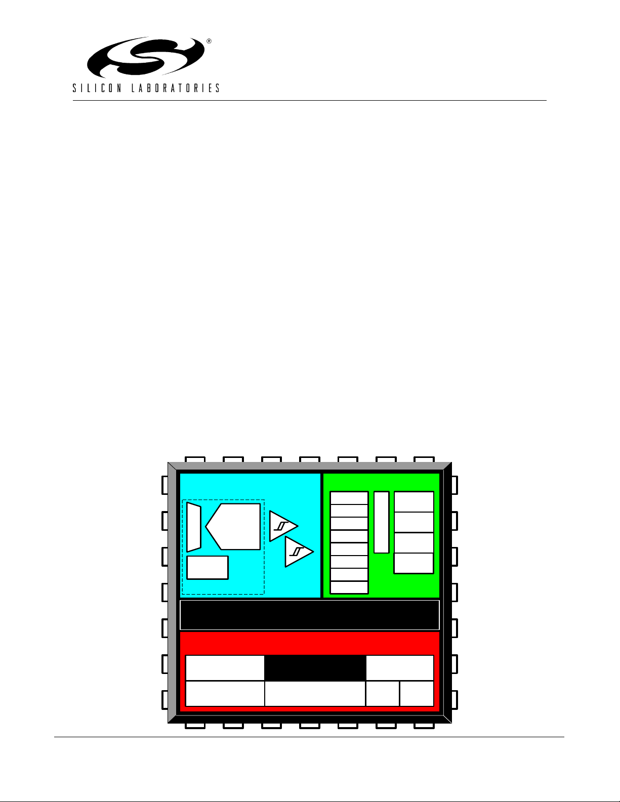
C8051F31x device s are fully integrated mixed-signal System-on-a-Chip MCUs. Highli ghted features are
listed below. Refer to
• High-speed pipelined 8051-compatible microcontroller core (up to 25 MIPS)
• In-system, full-speed, non-intrusive debug interface (on-chip)
• True 10-bit 200 ksps 25-channel single-ended/differential ADC with analog multiplexer
(C8051F310/1/2/3/6)
• Precision programmable 25 MHz internal oscillator
• 16 kB (C8051F310/1/6/7) or 8 kB (C8051F312/3/4/5) of on-chip Flash memory
• 1280 bytes of on-chip RAM
• SMBus/I2C, Enhanced UART , and Enhanced SPI serial interfaces implemented in hardware
• Four general-purpose 16-bit timers
• Programmable Counter/Timer Array (PCA) with five capture/compare modules and Watchdog Timer
function
• On-chip Power-On Reset, VDD Monitor, and Temperature Sensor
• On-chip Voltage Comparators (2)
• 29/25/21 Port I/O (5 V tolerant)
With on-chip Power-On Reset, VDD monitor, Watchdog Timer, and clock oscillator, the C8051F31x devices
are truly stand-alone Syste m-on-a-Chip solutions. The F lash memory can be reprogra mmed even in-cir
cuit, providing non-vo latil e data sto rage, and al so al lowin g field u pgrad es of the 805 1 firm ware. Us er software has complete c ontrol of all peripherals, and may individually shut down any or al l peripherals for
power savings.
Table 1.1 for specific product feature selection.
-
The on-chip Silicon Labs 2-Wire (C2) Development Interface allows non-intrusive (uses no on-chip
resources), full speed, in-circuit debugging using the production MCU installed in the final application. This
debug logic supports inspection and modification of memory and registers, setting breakpoints, single
stepping, run and halt commands. All a nalog and digital peripheral s are fully functional whi le debugging
using C2. The two C2 i nterface pins can be shared with us er functions, all owing in-system p rogramming
and debugging without occupying package pins.
Each device i s specifi ed for 2.7- to-3.6 V ope ration ove r the industr ial temper ature range ( –45 to +85 °C).
The Port I/O and
LQFP, 28-pin QFN, and 24-pin QFN packages. See
ages are also referred to as MLP or MLF packages.
RST pins are tolerant of inpu t signa ls up to 5 V. The C8051F31x are available in 32-pin
Table 1.1 for order i ng part num ber s. Note : QFN pac k-
Rev. 1.7 17
Page 18
C8051F310/1/2/3/4/5/6/7
Table 1.1. Product Selection Guide
Ordering Part Number
C8051F310 25 16 1280 3 3 3 3 3 3 29 3 3 2 - LQFP-32
C8051F310-GQ 25 16 1280 3 3 3 3 3 3 29 3 3 2 3 LQFP-32
C8051F311 25 16 1280 3 3 3 3 3 3 25 3 3 2 - QFN-28
C8051F311-GM 25 16 1280 3 3 3 3 3 3 25 3 3 2 3 QFN-28
C8051F312 25 8 1280 3 3 3 3 3 3 29 3 3 2 - LQFP-32
C8051F312-GQ 25 8 1280 3 3 3 3 3 3 29 3 3 2 3 LQFP-32
C8051F313 25 8 1280 3 3 3 3 3 3 25 3 3 2 - QFN-28
C8051F313-GM 25 8 1280 3 3 3 3 3 3 25 3 3 2 3 QFN-28
C8051F314 25 8 1280 3 3 3 3 3 3 29 - - 2 - LQFP-32
C8051F314-GQ 25 8 1280 3 3 3 3 3 3 29 - - 2 3 LQFP-32
C8051F315 25 8 1280 3 3 3 3 3 3 25 - - 2 - QFN-28
C8051F315-GM 25 8 1280 3 3 3 3 3 3 25 - - 2 3 QFN-28
C8051F316-GM 25 16 1280 3 3 3 3 3 3 21 3 3 2 3 QFN-24
C8051F317-GM 25 16 1280 3 3 3 3 3 3 21 - - 2 3 QFN-24
MIPS (Peak)
Flash Memory
RAM
Calibrated Internal 24.5 MHz Oscillator
SMBus/I2C
Enhanced SPI
UART
Timers (16-bit)
Programmable Counter Array
Digital Port I/Os
10-bit 200 ksps ADC
Temperature Sensor
Analog Comparators
Lead-free (RoHS Compliant)
Package
18 Rev. 1.7
Page 19
C8051F310/1/2/3/4/5/6/7
VDD
GND
/RST/C2CK
Analog/Digital
Power
C2D
XTAL1
XTAL2
POR
External
Oscillator
Circuit
2%
Internal
Oscillator
Debug HW
Brown-
Out
Reset
System Clock
8
0
5
1
C
o
SFR Bus
r
e
16kbyte
FLASH
256 byte
SRAM
1K byte
SRAM
Port 0
Latch
Port 1
Latch
UART
Timer
0,1,2,3 /
SMBus
Port 2
Latch
Port 3
Latch
VDD
10-bit
200ksps
ADC
RTC
PCA/
WDT
SPI
VREF
P
0
D
r
v
C
P
R
1
O
S
D
S
r
B
v
A
R
P
2
D
r
v
P
3
D
r
v
CP0
+
-
CP1
+
-
Temp
A
AIN0-AI N20
M
U
X
VDD
P0.0/VREF
P0.1
P0.2/XTAL1
P0.3/XTAL2
P0.4/TX
P0.5/RX
P0.6/CNVST
P0.7
P1.0
P1.1
P1.2
P1.3
P1.4
P1.5
P1.6
P1.7
P2.0
P2.1
P2.2
P2.3
P2.4
P2.5
P2.6
P2.7
P3.0/C2D
P3.1
P3.2
P3.3
P3.4
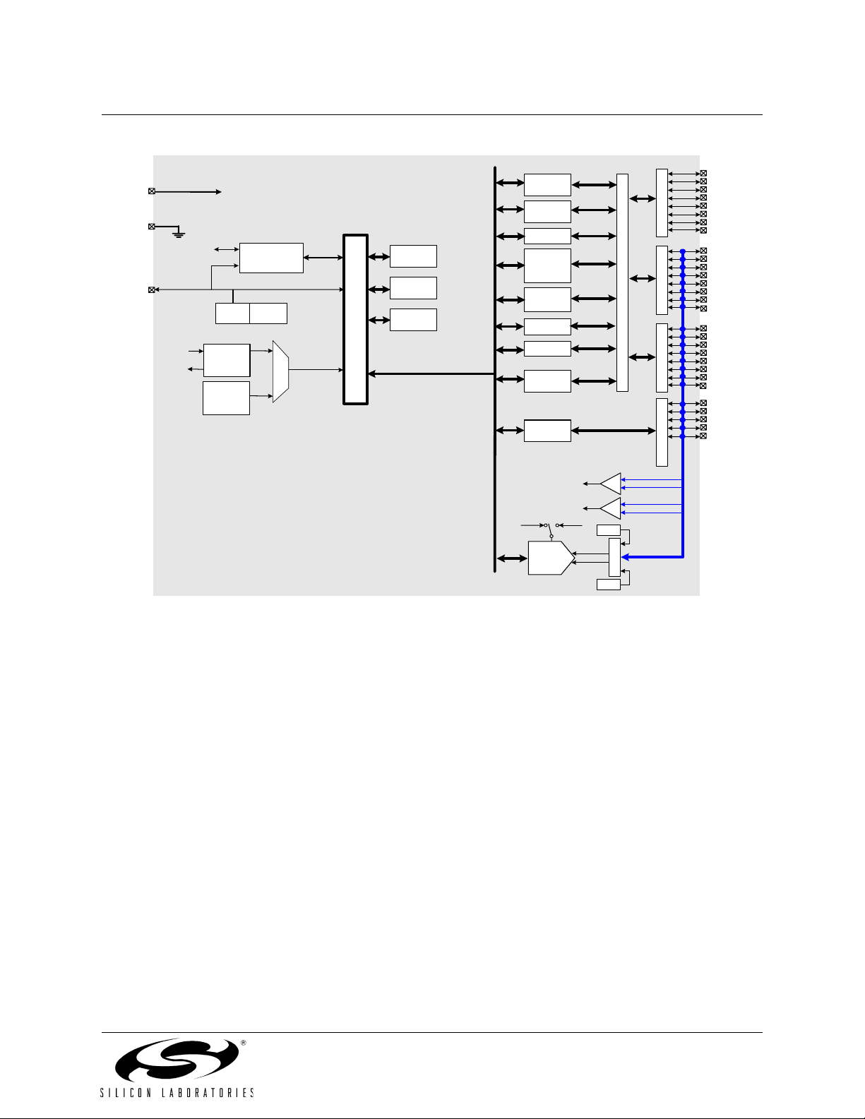
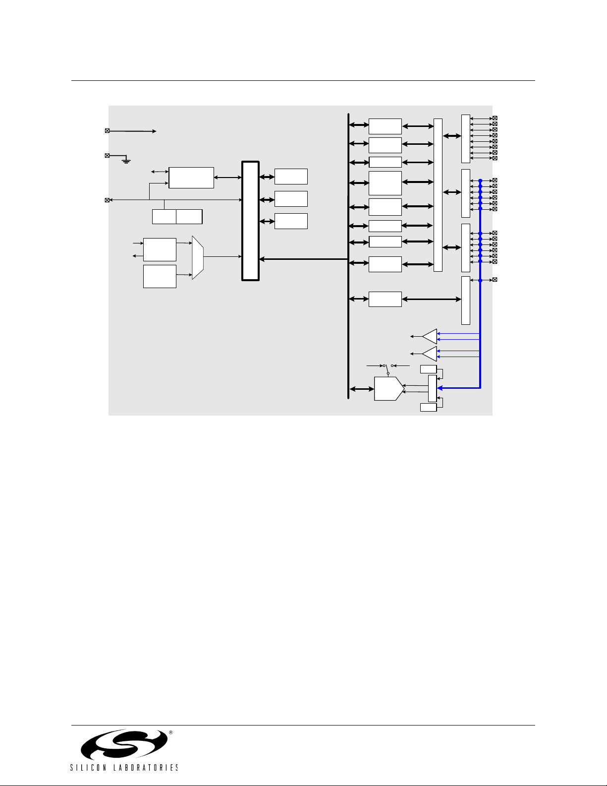
Figure 1.1. C8051F31 0 Block Diagr am
Rev. 1.7 19
Page 20
C8051F310/1/2/3/4/5/6/7
VDD
GND
/RST/C2CK
Analog/Digital
Power
C2D
XTAL1
XTAL2
POR
External
Oscillator
Circuit
2%
Internal
Oscillator
Debug HW
Brown-
Out
Reset
System Clock
8
0
5
1
C
o
SFR Bus
r
e
16kbyte
FLASH
256 byte
SRAM
1K byte
SRAM
Port 0
Latch
Port 1
Latch
UART
Timer
0,1,2,3 /
PCA/
WDT
SMBus
Port 2
Latch
Port 3
Latch
VDD
10-bit
200ksps
ADC
RTC
SPI
VREF
P
0
D
r
v
C
P
R
1
O
S
D
S
r
B
v
A
R
P
2
D
r
v
P
3
D
r
v
CP0
+
-
CP1
+
-
Temp
A
AIN0-AIN20
M
U
X
VDD
P0.0/VREF
P0.1
P0.2/XTAL1
P0.3/XTAL2
P0.4/TX
P0.5/RX
P0.6/CNVST
P0.7
P1.0
P1.1
P1.2
P1.3
P1.4
P1.5
P1.6
P1.7
P2.0
P2.1
P2.2
P2.3
P2.4
P2.5
P2.6
P2.7
P3.0/C2D
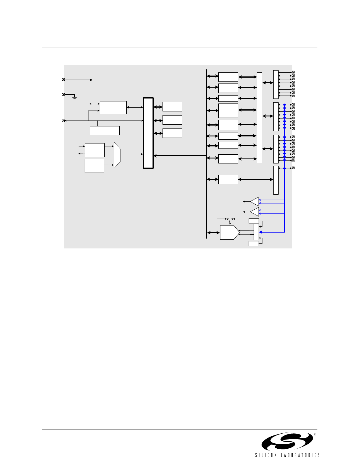
Figure 1.2. C8051F311 Block Diagram
20 Rev. 1.7
Page 21
C8051F310/1/2/3/4/5/6/7
VDD
GND
/RST/C2CK
Analog/Digital
Power
C2D
XTAL1
XTAL2
POR
External
Oscillator
Circuit
2%
Internal
Oscillator
Debug HW
Brown-
Out
Reset
System Clock
8
0
5
1
C
o
SFR Bus
r
e
8 kB
FLASH
256 byte
SRAM
1K byte
SRAM
Port 0
Latch
Port 1
Latch
UART
Timer
0,1,2,3 /
RTC
PCA/
WDT
SMBus
SPI
Port 2
Latch
Port 3
Latch
VDD
10-bit
200ksps
ADC
VREF
CP0
CP1
Temp
VDD
C
R
O
S
S
B
A
R
+
-
+
-
A
M
U
X
P
0
D
r
v
P
1
D
r
v
P
2
D
r
v
P
3
D
r
v
AIN0-AIN20
P0.0/VREF
P0.1
P0.2/XTAL1
P0.3/XTAL2
P0.4/TX
P0.5/RX
P0.6/CNVST
P0.7
P1.0
P1.1
P1.2
P1.3
P1.4
P1.5
P1.6
P1.7
P2.0
P2.1
P2.2
P2.3
P2.4
P2.5
P2.6
P2.7
P3.0/C2D
P3.1
P3.2
P3.3
P3.4
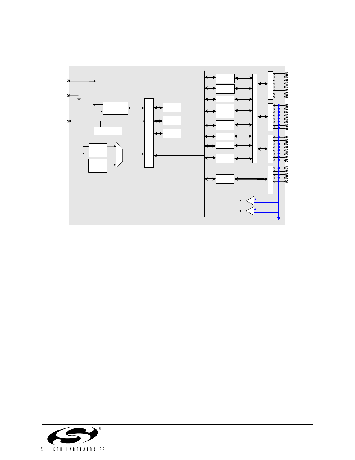
Figure 1.3. C8051F312 Block Diagram
Rev. 1.7 21
Page 22
C8051F310/1/2/3/4/5/6/7
VDD
GND
/RST/C2CK
Analog / Digital
Power
C2D
XTAL1
XTAL2
POR
External
Oscillator
Circuit
2%
Internal
Oscillator
Debug HW
Brown-
Out
Reset
System Clock
8
0
5
1
C
o
SFR Bus
r
e
8 kB
FLASH
256 byte
SRAM
1K byte
SRAM
Port 0
Latch
Port 1
Latch
UART
Timer
0,1,2,3 /
RTC
PCA/
WDT
SMBus
Port 2
Latch
Port 3
Latch
VDD
10-bit
200ksps
ADC
SPI
VREF
CP1
CP0
Temp
VDD
C
R
O
S
S
B
A
R
+
-
+
-
A
M
U
X
P
0
D
r
v
P
1
D
r
v
P
2
D
r
v
P
3
D
r
v
AIN0-AIN20
P0.0/VREF
P0.1
P0.2/XTAL1
P0.3/XTAL2
P0.4/TX
P0.5/RX
P0.6/CNVST
P0.7
P1.0
P1.1
P1.2
P1.3
P1.4
P1.5
P1.6
P1.7
P2.0
P2.1
P2.2
P2.3
P2.4
P2.5
P2.6
P2.7
P3.0/C2D
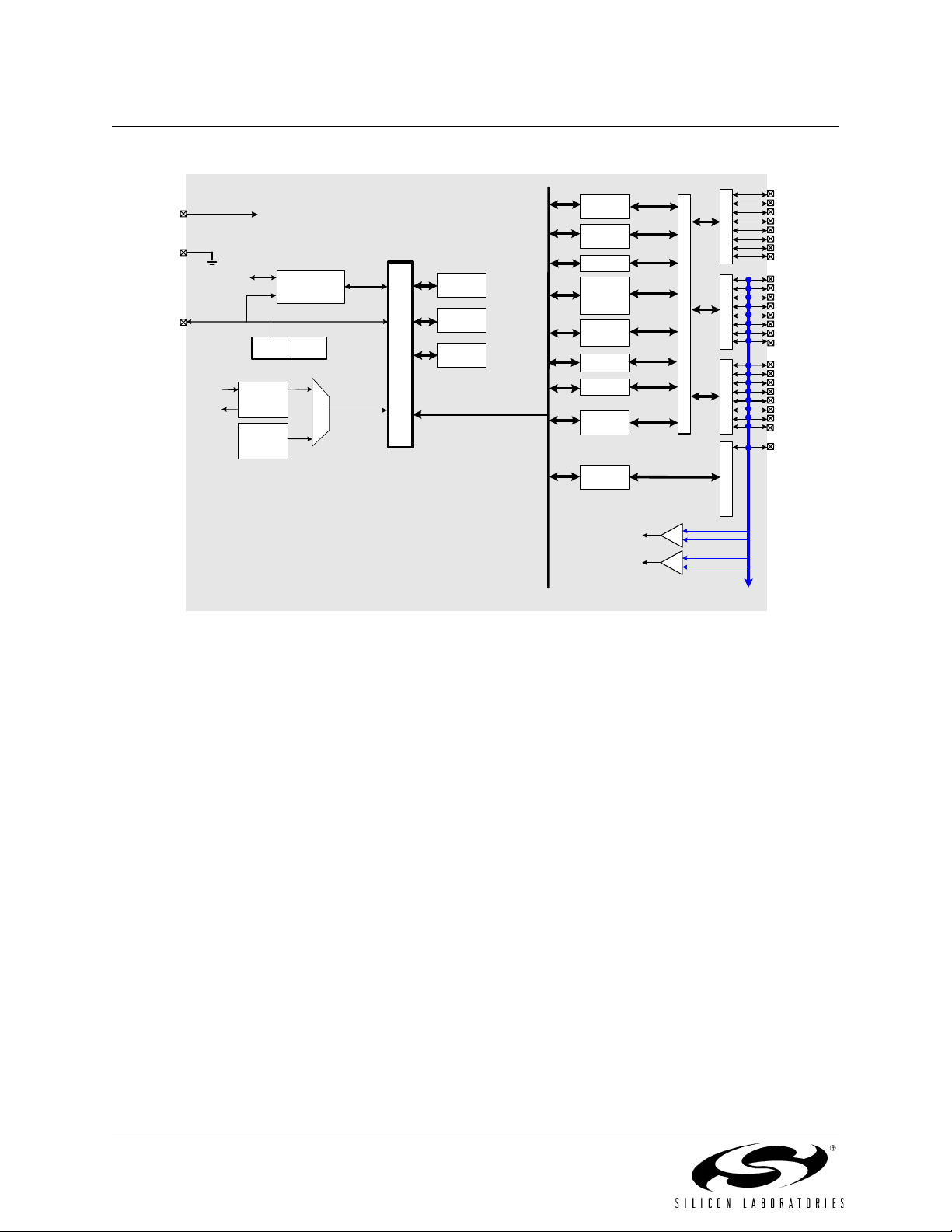
Figure 1.4. C8051F313 Block Diagram
22 Rev. 1.7
Page 23
C8051F310/1/2/3/4/5/6/7
VDD
GND
/RST/C2CK
Analog/Digital
Power
C2D
XTAL1
XTAL2
POR
External
Oscillator
Circuit
2%
Internal
Oscillator
Debug HW
Brown-
Out
Reset
8
0
5
1
8 kB
FLASH
256 byte
SRAM
1K byte
SRAM
C
System Clock
o
SFR Bus
r
e
Figure 1.5. C8051F314 Block Diagram
Port 0
Latch
Port 1
Latch
UART
Timer
0,1,2,3 /
RTC
PCA/
WDT
SMBus
SPI
Port 2
Latch
Port 3
Latch
P
0
D
r
v
C
P
R
1
O
S
D
S
r
B
v
A
R
P
2
D
r
v
P
3
D
r
v
CP0
+
-
CP1
+
-
P0.0/VREF
P0.1
P0.2/XTAL1
P0.3/XTAL2
P0.4/TX
P0.5/RX
P0.6/CNVST
P0.7
P1.0
P1.1
P1.2
P1.3
P1.4
P1.5
P1.6
P1.7
P2.0
P2.1
P2.2
P2.3
P2.4
P2.5
P2.6
P2.7
P3.0/C2D
P3.1
P3.2
P3.3
P3.4
Rev. 1.7 23
Page 24
C8051F310/1/2/3/4/5/6/7
VDD
GND
/RST/C2CK
Analog/Digital
Power
C2D
XTAL1
XTAL2
POR
External
Oscillator
Circuit
2%
Internal
Oscillator
Debug HW
Brown-
Out
Reset
System Clock
8
0
5
1
C
o
SFR Bus
r
e
8 kB
FLASH
256 byte
SRAM
1K byte
SRAM
Port 0
Latch
Port 1
Latch
UART
Timer
0,1,2,3 /
RTC
PCA/
WDT
SMBus
SPI
Port 2
Latch
Port 3
Latch
P
0
D
r
v
C
P
R
1
O
R
CP0
+
-
CP1
+
-
S
D
S
r
B
v
A
P
2
D
r
v
P
3
D
r
v
P0.0/VREF
P0.1
P0.2/XTAL1
P0.3/XTAL2
P0.4/TX
P0.5/RX
P0.6/CNVST
P0.7
P1.0
P1.1
P1.2
P1.3
P1.4
P1.5
P1.6
P1.7
P2.0
P2.1
P2.2
P2.3
P2.4
P2.5
P2.6
P2.7
P3.0/C2D
Figure 1.6. C8051F315 Block Diagram
24 Rev. 1.7
Page 25
C8051F310/1/2/3/4/5/6/7
/
T
VDD
GND
RST/C2CK
Analog/Digital
Power
C2D
XTAL1
XTAL2
POR
External
Oscillator
Circuit
2%
Internal
Oscillator
Debug HW
Brown-
Out
Reset
System Clock
8
0
5
1
C
o
SFR Bus
r
e
16 kB
FLASH
256 byte
SRAM
1 kB
SRAM
Port 0
Latch
Port 1
Latch
UART
Timer
0,1,2,3 /
PCA/
SMBus
Port 2
Latch
Port 3
Latch
VDD
10-bit
200 ksps
ADC
RTC
WDT
SPI
VREF
CP0
CP1
Temp
VDD
A
M
U
X
+
-
+
-
C
R
O
S
S
B
A
R
P
0
D
r
v
P
1
D
r
v
P
2
D
r
v
P
3
D
r
v
AIN0–AIN20
P0.0/VR EF
P0.1
P0.2/XT A L1
P0.3/XT A L2
P0.4/TX
P0.5/RX
P0.6/CN VS
P0.7
P1.0
P1.1
P1.2
P1.3
P1.4
P1.5
P2.0
P2.1
P2.2
P2.3
P2.4
P2.5
P3.0/C2 D
Figure 1.7. C8051F316 Block Diagram
Rev. 1.7 25
Page 26

C8051F310/1/2/3/4/5/6/7
VDD
GND
/RST/C2CK
Analog/Digital
Power
C2D
XTAL1
XTAL2
POR
External
Oscillator
Circuit
2%
Internal
Oscillator
Debug HW
Brown-
Out
Reset
8
0
5
1
16 kB
FLASH
256 byte
SRAM
1 kB
SRAM
C
System Clock
o
SFR Bus
r
e
Figure 1.8. C8051F317 Block Diagram
Port 0
Latch
Port 1
Latch
UART
Timer
0,1,2,3 /
RTC
PCA/
WDT
SMBus
SPI
Port 2
Latch
Port 3
Latch
P
0
D
r
v
C
P
R
1
O
S
D
S
r
B
v
A
R
P
2
D
r
v
P
3
D
r
v
CP0
+
-
CP1
+
-
P0.0/VREF
P0.1
P0.2/XTAL1
P0.3/XTAL2
P0.4/TX
P0.5/RX
P0.6/CNVST
P0.7
P1.0
P1.1
P1.2
P1.3
P1.4
P1.5
P2.0
P2.1
P2.2
P2.3
P2.4
P2.5
P3.0/C2D
26 Rev. 1.7
Page 27
C8051F310/1/2/3/4/5/6/7
k)
1.1. CIP-51™ Microcontroller Core
1.1.1. Fully 8051 Compatible
The C8051F31x family utilizes Silicon Laboratories' proprietary CIP-51 microcontroller core. The CIP-51 is
fully compatible with t he MCS -51™ instruc tion s et; s tandard 80 3x/80 5x as sembl ers and comp ilers ca n be
used to develop software. The CIP-51 core offers all the peripherals included with a standard 8052, includ
ing four 16-bit counter/timers, a full-duplex UART with extended baud rate configuration, an enhanced SPI
port, 1280
I/O pins.
1.1.2. Improved Throughput
The CIP-51 employs a pipelined architecture that greatly increases its instruction throughput over the standard 8051 architecture. In a standard 8051, all ins truction s except for MU L and DIV take 12 or 24 syste m
clock cycles to execute wi th a maximu m sys tem clock of 12-to- 24
cutes 70% of its instructions in one or two system clock cycles, with only four instructions taking more than
four system clock cycles.
The CIP-51 has a total of 109 instructions. The table below shows the total number of instructions that
require each execution time.
bytes of internal RAM , 128 byte Special Function Register (SFR) address space, and 29/25/2 1
MHz. By contrast, the CIP- 51 core exe-
-
Clocks to Execute 1 2 2/3 3 3/4 4 4/5 5 8
Number of Instructions 26 50 5 14 7 3 1 2 1
With the CIP-51's maximum system clock at 25 MHz, it has a peak throughput of 25 MIPS. Figure 1.9
shows a comparison of peak throu ghputs for various 8-bit micro controller cores wit h their maximum system clocks.
25
20
15
MIPS
10
5
Silicon Labs
CIP-51
(25 MHz clk)
Microchip
PIC17C75x
(33 MHz clk)
Philips
80C51
(33 MHz clk)
ADuC812
8051
(16 MHz cl
Figure 1.9. Comparison of Peak MCU Execution Speeds
Rev. 1.7 27
Page 28
C8051F310/1/2/3/4/5/6/7
1.1.3. Additional Features
The C8051F31x SoC famil y includes several key enhancements to the CIP-51 co re and peripherals to
improve performance and ease of use in end applications.
The extended interrupt handler provides 14 interrupt sources into the CIP-51 (as opposed to 7 for the standard 8051), allowing numerous analog and digital peripherals to interrupt the controller. An interrupt driven
system requires less intervention by the MCU, giving it more effective throughput. The extra interrupt
sources are very useful when building multi-tasking, real-time systems.
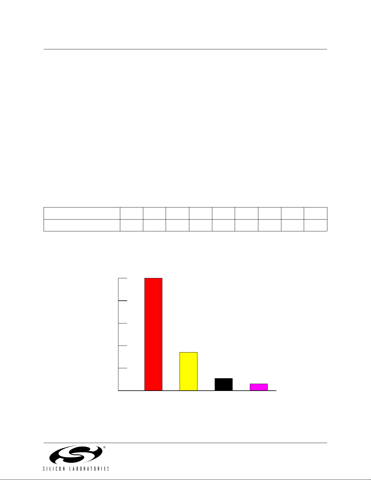
Eight reset source s are available: power-on r eset circuitry (POR), an on-c hip VDD monitor (forces reset
when power supply voltage drops below V
Missing Clock Detec tor, a voltage level detection from Comparator0, a forc ed software reset, an exter nal
reset pin, and an er rant Flash read/wr ite protection c ircuit. Each r eset source excep t for the POR, R eset
Input Pin, or Flash err or may b e dis abled by the use r in soft ware. Th e WDT ma y be pe rman ently ena bled
in software after a power-on reset during MCU initialization.
The internal oscillator is factory calibrated to 24.5 MHz ±2%. An external oscillator drive circuit is also
included, allowing an external crystal, ceramic resonator, capacitor, RC, or CMOS clock source to generate
the system clock. If desi red, the system clock sourc e ma y b e swi tc hed on- the -f ly betw een the internal and
external oscillato r circuits. An ex ternal oscill ator can be extremely us eful in low p ower applica tions, allow
ing the MCU to run from a slow (power savi ng) exter nal crystal s ource, whil e perio dically swi tching to the
fast internal oscillator as needed.
as given in Table 9.1 on page 110), a Watchdog Timer, a
RST
-
XTAL1
XTAL2
Internal
Oscillator
External
Oscillator
Drive
Px.x
Px.x
VDD
Power On
Supply
Monitor
Comparator 0
+
-
System
Clock
Clock Select
C0RSEF
Missing
Clock
Detector
(oneshot)
EN
MCD
Enable
CIP-51
Microcontroller
PCA
WDT
EN
WDT
Enable
+
-
System Reset
Enable
(Software Reset)
SWRSF
'0'
Core
Extended Interrupt
Handler
Figure 1.10. On-Chip Clock and Reset
Reset
Errant
FLASH
Operation
(wired-OR)
Reset
Funnel
/RST
28 Rev. 1.7
Page 29
C8051F310/1/2/3/4/5/6/7
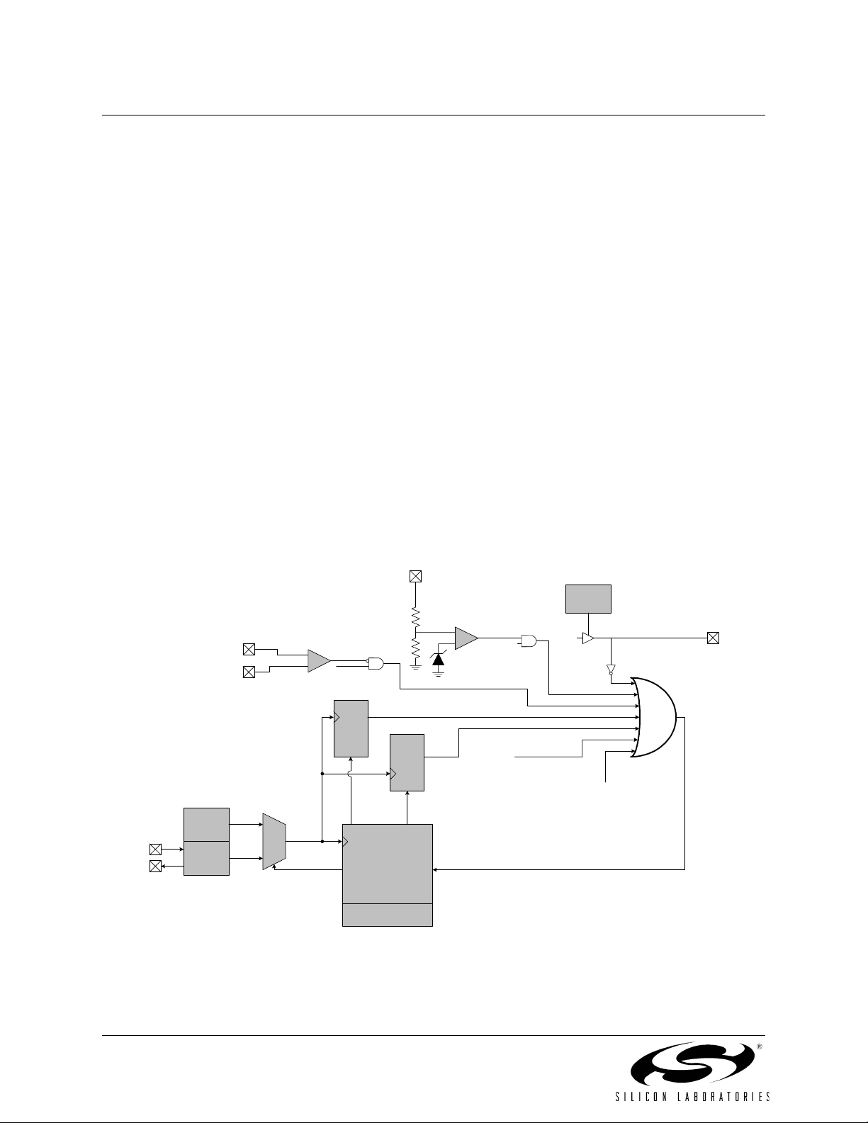
1.2. On-Chip Memory
The CIP-51 has a standa rd 8051 program and data addres s configuration. It inclu des 256 bytes of data
RAM, with the upper 128 bytes dual-mapped. Indirect addressing accesses the upper 128 bytes of general
purpose RAM, and direct add ressing acce sses the 128 byte SFR address space. The lower 128 bytes of
RAM are accessible via direct and indirect addressing. The first 32 bytes are addressable as four banks of
general purpose registers, and the next 16 bytes can be byte addressable or bit addressable.
Program memory con sists of 8 or 16 kB of Fl ash. This memory ma y be reprogramm ed in-system in 51 2
byte sectors, and requi res no specia l off-chip program ming voltage. See
memory map.
Figure 1.11 for the MCU system
PROGRAM/DATA MEMORY
(Flash)
C8051F310/1/6/7
0x3E00
0x3DFF
0x0000
0x2000
0x1FFF
RESERVED
16 kB Flash
(In-System
Programmab le in 5 12
Byte Sectors)
C8051F31 2/3/4/5
RESERVED
0xFF
0x80
0x7F
0x30
0x2F
0x20
0x1F
0x00
0xFFFF
DATA MEMORY (RAM)
INTERNAL DATA ADDRESS SPACE
Upper 128 RAM
(Indirect Addressing
Only)
(Direct and Indirect
Addressing)
Bit Addressable
Gene ra l P u rpo s e
Registers
Special Function
Register's
(Direct Addressing Only)
Lower 128 RA M
(Direct and Indirect
Addressing)
EXTERNAL DATA ADDRESS SPACE
Same 1024 bytes as from
0x0000 to 0x03FF, wrapped
on 1 kB boundaries
0x0000
8 kB Flash
(In-System
Programmab le in 5 12
Byte Sectors)
Figure 1.11. On-Board Memory Map
0x0400
0x03FF
0x0000
XRAM - 1024 Bytes
(accessable using MOVX
instruction)
Rev. 1.7 29
Page 30
C8051F310/1/2/3/4/5/6/7
1.3. On-Chip Debug Circuitry
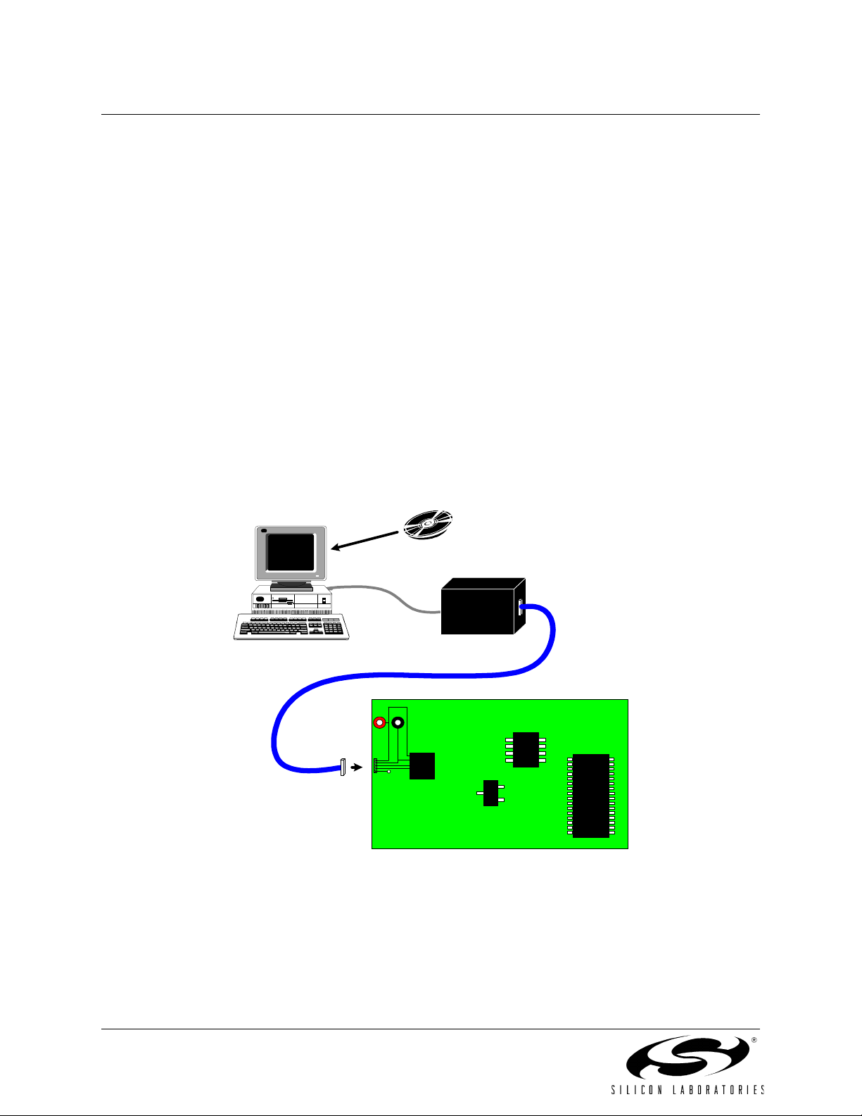
The C8051F31x device s include on- chip Silicon Lab s 2-Wire (C2) debug circuitry that provides non-i ntrusive, full speed, in-circuit debugging of the production part installed in the end application.
Silicon Labs' debugging system supports inspection and modification of memory and registers, breakpoints, and single stepping. No additi onal target RAM , progra m memory, timers, or communication s channels are required. Al l th e d ig ital an d a nal og peri pher a ls ar e functi ona l a nd wor k co rre ctly whi le deb ugg ing .
All the peripherals (except for the ADC and SMB us) are stalled when the MCU is halted, during singl e
stepping, or at a breakpoint in order to keep them synchronized.
The C8051F310DK development kit provides all the hardware and software necessary to develop application code and perfo rm in-circuit debugging wi th the C8051F31x MCUs. Th e kit includes software with a
developer's studio and debugger, an integrated 8051 assembler, a debug adapter, a target application
board with the associated MCU installed, and the required cables and wall-mount power supply.
The Silicon Labs IDE interf ace is a vastl y superio r developing and debuggi ng configurati on, compared t o
standard MCU emulators that use on-b oard "ICE Chips" and require the MCU in the application board to
be socketed. Silico n Labs' debug paradigm incr eases ease of use and p reserves the performa nce of the
precision analog peripherals.
Silicon Labo ratories Integrated
Development Environment
Windows 98SE or later
Debug
Adapter
C2 (x2), VDD, GND
VDD GND
C8051F31x
TARGET PCB
Figure 1.12. Development/In-System Debug Diagram
30 Rev. 1.7
Page 31

C8051F310/1/2/3/4/5/6/7
1.4. Programmable Digital I/O and Crossbar
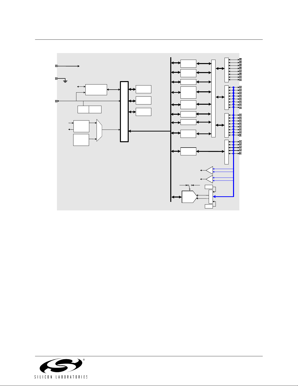
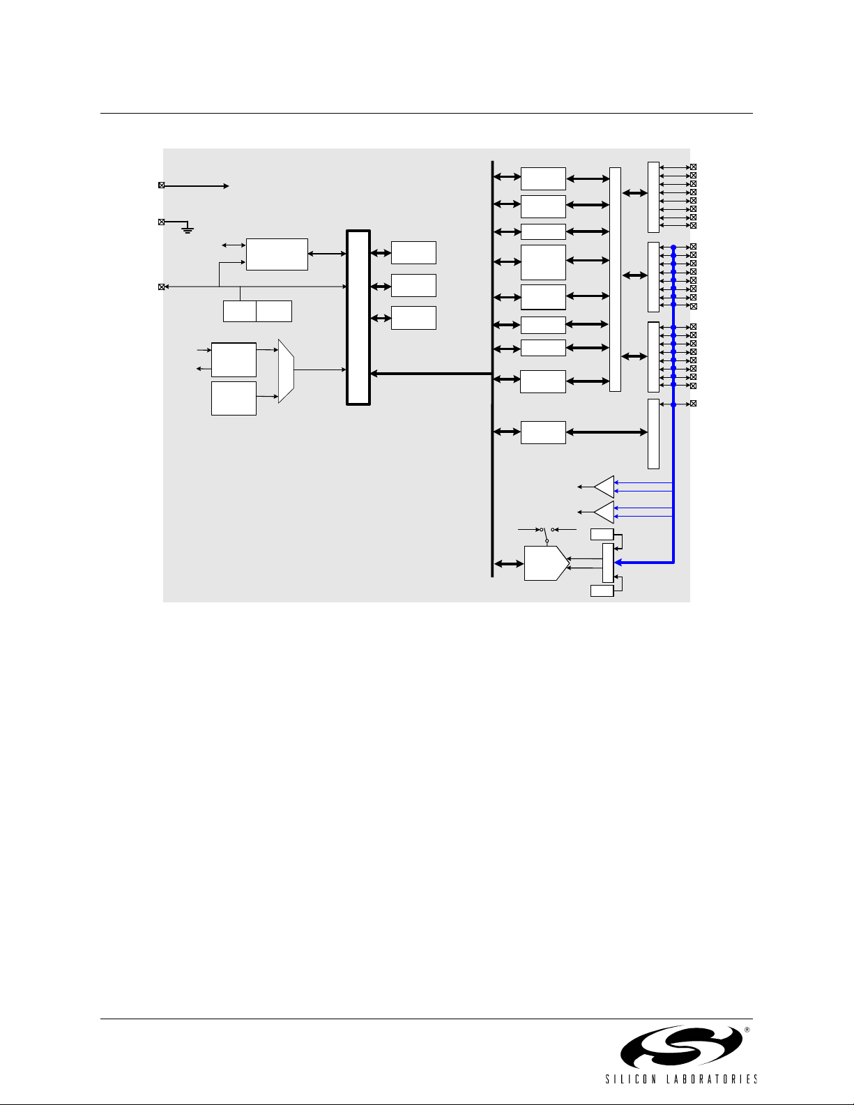
C8051F310/2/4 devices include 29 I/O pins (three byte-wide Ports and one 5-bit-wide Port);
C8051F311/3/5 devices include 25 I/O pi ns (thr ee by te-wide Ports and one 1-bit-wi de P ort) ; C8 051 F 316/ 7
devices include 21 I/O pins (one byte-wide Port, two 6-bit-wide Ports and one 1-bit-wide Port). The
C8051F31x Ports behav e like typica l 8051 Ports with a few e nhanceme nts. Each Po rt pin may be config
ured as an analog inp ut o r a di gital I/ O pin . Pi ns s ele ct ed a s d ig ital I/O s may a ddi tio nal ly be co nfi gured for
push-pull or open-dr ain output. T he “weak pu llups” that a re fixed on ty pical 80 51 devices may be global ly
disabled, providing power savings capabilities.
The Digital Crossbar allows mapping of internal digital system resources to Port I/O pins (See Figure 1.13).
On-chip counter/timers, serial buses, HW interrupts, comparator output, and other digital signa ls in the
controller can be configured to appear on the Port I/O pins specified in the Crossbar Control registers. This
allows the user to select the exact mix of general purpose Por t I/O and digital resources needed for th e
particular application.
-
Highest
Priority
Lowest
Priority
XBR0, XBR1,
PnSKIP Registers
PnMDOUT,
PnMDIN Registers
Priority
Decoder
(P0.0-P0.7)
(P1.0-P1.7)
(P2.0-P2.3)
(P2.4-P2.7)
(P3.0-P3.4)
2
4
2
2
2
6
2
8
8
4
4
5
Digital
Crossbar
8
8
4
P0
I/O
Cells
P1
I/O
Cells
P2
84
I/O
Cells
P3
5
I/O
Cells
Notes:
1. P3.1–P3.4 only available on the
C8051F310/2/4.
2. P1.6, P1.7, P2.6, P2.7 only
available on the C8051F310/1/2/3/4/5
P0.0
P0.7
P1.0
P1.7
P2.0
P2.7
P3.0
P3.4
UART
SPI
SMBus
CP0
Outputs
CP1
Outputs
SYSCLK
(Internal Digital Signals)
PCA
T0, T1
P0
P1
(Port Latches)
P2
P3
Figure 1.13. Digital Crossbar Diagram
Rev. 1.7 31
Page 32

C8051F310/1/2/3/4/5/6/7
1.5. Serial Ports
The C8051F31x Family includ es an SMBus/I2C interface, a full-duplex UA RT with enhanced baud rate
configuration, an d an Enhanced S PI interface. Eac h of the seri al buses is fully implemented in hardware
and makes extensive use of the CIP-51's interrupts, thus requiring very little CPU intervention.
1.6. Programmable Counter Array
An on-chip Programmable Counter/Timer Array (PCA) is included in addition to the four 16-bit general purpose counter/timers. The PCA consists of a dedicated 16-bit counter/timer time base with five programmable capture/compare modules. The PCA clock is derived from one of six sources: the system clock divided
by 12, the system clock divided by 4, Timer 0 overflows, an External Clock Input (ECI), the system clock, or
the external oscilla tor c lock s our ce di vi de d by 8 . T he ext er nal cloc k s ourc e s ele ct ion is useful for real - tim e
clock functionality, where the PCA is cloc ked by a n exter nal source while th e inter nal oscilla tor drives the
system clock.
Each capture/compare module can be configured to operate in one of six modes: Edge-Triggered Capture,
Software Timer, High S peed Output, 8- or 16-bit Pulse Width Modulator, or Frequency Output. Additionally,
Capture/Compare Module 4 offers watchdog timer (WDT) capabilities. Following a system reset, Module 4
is configured and enabled in WDT mode. The PCA Capture/Compare Module I/O and External Clock Input
may be routed to Port I/O via the Digital Crossbar.
SYSCLK/12
SYSCLK/4
Timer 0 Overflow
ECI
SYSCLK
External Clock/8
Capture/Compare
Module 0
ECI
CEX0
PCA
CLOCK
MUX
Capture/Compare
Module 1
CEX1
16-Bit Counter/Timer
Capture/Compare
Module 2
CEX2
Capture/Compare
Module 3
CEX3
Capture/Compare
Module 4 / WDT
CEX4
Crossbar
Port I/O
Figure 1.14. PCA Block Diagram
32 Rev. 1.7
Page 33

C8051F310/1/2/3/4/5/6/7
1.7. 10-Bit Analog to Digital Converter
The C8051F310/1/2/3/6 devices include an on-chip 10-bit SAR ADC with a 25-cha nnel differential input
multiplexer. With a maximum throug hput of 200
±1LSB. The ADC system include s a configurab le analog multip lexer that selec ts both positive an d nega
tive ADC inputs. Ports1-3 are availa ble as an ADC inputs; additionally, the on-chip Temperature Sensor
output and the power supply voltage (V
DD
ADC to save power.
Conversions can be started in six ways: a software command, an overflow of Timer 0, 1, 2, or 3, or an
external convert start signal. This flexibility allows the start of conversion to be triggered by software
events, a periodic sig nal (timer ove rflows), or e xternal HW sig nals. Convers ion completi ons are ind icated
by a status bit and an interrupt (if enabled) . The resulting 10-bit data word is latched into the ADC da ta
SFRs upon completion of a conversion.
Window compare registers for the ADC data can be configured to interrupt the controller when ADC data is
either within or o utside of a specified range. The ADC can monitor a key voltage continuously in back
ground mode, but not interrupt the controller unless the converted data is within/outside the specified
range.
ksps, the ADC offers true 10-bit accuracy with an INL of
-
) are available as ADC inputs. User firmware may shut down the
-
Analog Multiplexer
P1.6, P1.7 available on
C8051F310/1/2/3/4/5
P2.6, P2.7 available on
C8051F310/1/2/3/4/5
P3.1-3.4
available on
C8051F310/2
Temp
Sensor
P1.6, P1.7 available on
C8051F310/1/2/3/4/5
P2.6, P2.7 available on
C8051F310/1/2/3/4/5
P3.1-3.4
available on
C8051F310/2
P1.0
P1.7
P2.0
P2.7
P3.0
P3.4
VDD
P1.0
P1.7
P2.0
P2.7
P3.0
P3.4
VREF
GND
23-to-1
AMUX
23-to-1
AMUX
Configuration, Control, and Data Registers
(+)
10-Bit
SAR
(-)
ADC
End of
Conversion
Interrupt
Start
Conversion
16
Window Compare
000 AD0BUSY (W)
001
Timer 0 Overflow
010
Timer 2 Overflow
Timer 1 Overflow
011
CNVSTR Input
100
Timer 3 Overflow
101
ADC Data
Registers
Window
Logic
Compare
Interrupt
Figure 1.15. 10-Bit ADC Block Diagram
Rev. 1.7 33
Page 34

C8051F310/1/2/3/4/5/6/7
1.8. Comparators
C8051F31x devices include two on-chip voltage comparators that are enabled/disabled and configured via
user software. Port I/O pins may be c on fig ur ed as compara tor in puts vi a a sel ec tio n mu x. Two comparator
outputs may be routed to a Port pin if desired: a latched output and/or an unlatched (asynchronous) output.
Comparator response time is programmable, allowing the user to select between high-speed and lowpower modes. Positive and negative hysteresis are also configurable.
Comparator interrupts may be generated on rising, falling, or both edges. When in IDLE mode, these interrupts may be used as a “wake-up” source. Comparator0 may also be configured as a reset source.
Figure 1.16 shows he Comparator0 block diagram.
CP0EN
CP0OUT
CMX0N1
CMX0N0
CPT0MX
CMX0P1
CMX0P0
P1.0
P1.4
P2.0
P2.4
P1.1
P1.5
P2.1
P2.5
CP0RIF
CP0FIF
CP0HYP1
CPT0CN
CP0HYP0
CP0HYN1
CP0HYN0
CP0 +
CP0 -
VDD
CP0
Interrupt
CP0
Rising-edge
CP0
Falling-edge
Interrupt
Logic
+
-
SET
SET
Q
D
D
Q
CLR
CLR
(SYNCHRONIZER)
Q
Q
Crossbar
GND
CP0
CP0A
Reset
Decision
Tree
CP0RIE
CP0FIE
CPT0MD
CP0MD1
CP0MD0
Figure 1.16. Comparator0 Block Diagram
34 Rev. 1.7
Page 35

2. Absolute Maximum Ratings
C8051F310/1/2/3/4/5/6/7
Table 2.1. Absolute Maximum Ratings
Parameter Conditions Min Typ Max Units
Ambient temperature under bias –55 — 125 °C
Storage Temperature –65 — 150 °C
Voltage on any Port I/O Pin or RST
respect to GND
Voltage on V
Maximum Total current through V
GND
Maximum output current sunk by RST
Port pin
*Note: Stresses above those listed under “Absolute Maximum Ratings” may cause permanent damage to
the device. This is a stress rating only and functional operation of the devices at those or any other conditions above those indicated in the operation listings of this specification is not implied. Exposure to maximum rating conditions for extended periods may affect device reliability.
with respect to GND –0.3 — 4.2 V
DD
with
DD
and
or any
–0.3 — 5.8 V
——500mA
——100mA
*
Rev. 1.7 35
Page 36

C8051F310/1/2/3/4/5/6/7
3. Global DC Electrical Characteristics
Table 3.1. Global DC Electrical Characteristics
–40°C to +85°C, 25 MHz System Clock unless otherwise specified.
Parameter Conditions Min Typ Max Units
Digital Supply Voltage
Digital Supply RAM Data Retention
Voltage
Specified Operating Temperature
Range
SYSCLK (system clock frequency)
Tsysl (SYSCLK low time) 18 — — ns
Tsysh (SYSCLK high time)
Digital Supply Current—CPU Active (Normal Mode, fetching instructions from Flash)
I
(Note 3) V
DD
Supply Sensitivity (Note 3,
I
DD
Note 4)
I
Frequency Sensitivity (N ote 3 ,
DD
Note 5)
VDD = 3.0 V, F < 15 MHz, T = 25 ºC — 0.39 — mA/MHz
V
DD
V
DD
V
DD
= 3.0 V , F = 25 MHz — 7.8 8.6 mA
DD
= 3.0 V , F = 1 MHz — 0.38 — mA
V
DD
= 3.0 V , F = 80 kHz — 31 — µA
V
DD
= 3.6 V , F = 25 MHz — 10.7 12.1 mA
V
DD
F = 25 MHz — 67 — %/V
F = 1 MHz — 62 — %/V
= 3.0 V, F > 15 MHz, T = 25 ºC — 0.21 — mA/MHz
= 3.6 V, F < 15 MHz, T = 25 ºC — 0.55 — mA/MHz
= 3.6 V, F > 15 MHz, T = 25 ºC — 0.27 — mA/MHz
Notes:
1. Given in Table 9.1 on page 110.
2. SYSCLK must be at least 32 kHz to enable debugging.
3. Based on device characteriz ation data, not produ cti on test ed.
4. Active and Inactive I
using the I
Supply Sensitivity. For example, if the VDD is 3.3 V instead of 3.0 V at 25 MHz: IDD =
DD
7.8 mA typical at 3.0 V and f = 25 MHz. From this, I
at voltages and frequenci es other than those spec ified can be calculate d
DD
= 7.8 mA + 0.67 x (3.3 V – 3.0 V) = 8 mA at
DD
3.3 V and f = 25 MHz.
5. I
can be estimated for frequen cies < 15 MHz by m ultipl ying the frequ ency of inte rest by the fr e-
DD
quency sensitivity number for that range. When using these numbers to estimate I
the estimate should be the current a t 25 MHz m inus the d ifference in current i ndicated by the fre-
quency sensitivity number. For example:
V
= 3.0 V; F = 20 MHz, IDD = 7.8 mA – (25 MHz – 20 MHz) x 0.21 mA/MHz = 6.75 mA.
DD
6. Idle I
can be estimated for frequencie s < 1 MHz by mul tiplying the fr equency o f interest by the
DD
frequency sensitivity number for that range. When using these numbers to estimate Idle I
MHz, the estimate should be the current at 25 MHz minus the difference in current indicated by the
frequency sensitivity number. For example:
V
= 3.0 V; F = 5 MHz, Idle IDD = 4.8 mA – (25 MHz – 5 MHz) x 0.15 mA/MHz = 1.8 mA.
DD
1
V
RST
3.0 3.6 V
—1.5— V
–40 — +85 °C
2
0
—25MHz
18 — — ns
for > 15 MHz,
DD
for > 1
DD
36 Rev. 1.7
Page 37

C8051F310/1/2/3/4/5/6/7
Table 3.1. Global DC Electrical Characteristics (Continued)
–40°C to +85°C, 25 MHz System Clock unless otherwise specified.
Parameter Conditions Min Typ Max Units
Digital Supply Current—CPU Inactive (Idle Mode, not fetching instructions from Flash)
I
(Note 3)
DD
Supply Sensitivity (Note 3,
I
DD
Note 4)
V
= 3.0 V, F = 25 MHz
DD
V
= 3.0 V, F = 1 MHz
DD
V
= 3.0 V, F = 80 kHz
DD
V
= 3.6 V, F = 25 MHz
DD
F = 25 MHz
F = 1 MHz
—3.84.3mA
—0.20— mA
—16—µA
—4.85.3mA
—44—%/V
—56—%/V
Frequency Sensitivity (N ote 3 ,
I
DD
Note 6)
Digital Supply Current
(Stop Mode, shutdown)
V
= 3.0 V, F < 1 MHz, T = 25 °C
DD
V
= 3.0 V, F > 1 MHz, T = 25 °C
DD
V
= 3.6 V, F < 1 MHz, T = 25 °C
DD
V
= 3.6 V, F > 1 MHz, T = 25 °C
DD
Oscillator not running,
V
Monitor Disabled
DD
— 0.21 — mA/MHz
— 0.15 — mA/MHz
— 0.28 — mA/MHz
— 0.19 — mA/MHz
—< 0.1— µA
Notes:
1. Given in Table 9.1 on page 110.
2. SYSCLK must be at least 32 kHz to enable debugging.
3. Based on device characteriz ation data, not produ cti on test ed.
4. Active and Inactive I
using the I
Supply Sensitivity. For example, if the VDD is 3.3 V instead of 3.0 V at 25 MHz: IDD =
DD
7.8 mA typical at 3.0 V and f = 25 MHz. From this, I
at voltages and frequenci es other than those spec ified can be calculate d
DD
= 7.8 mA + 0.67 x (3.3 V – 3.0 V) = 8 mA at
DD
3.3 V and f = 25 MHz.
5. I
can be estimated for frequen cies < 15 MHz by m ultipl ying the frequ ency of inte rest by the fr e-
DD
quency sensitivity number for that range. When using these numbers to estimate I
for > 15 MHz,
DD
the estimate should be the current a t 25 MHz m inus the d ifference in current i ndicated by the frequency sensitivity number. For example:
V
= 3.0 V; F = 20 MHz, IDD = 7.8 mA – (25 MHz – 20 MHz) x 0.21 mA/MHz = 6.75 mA.
DD
6. Idle I
frequency sensitivity number for that range. When using these numbers to estimate Idle I
can be estimated for frequencie s < 1 MHz by mul tiplying the fr equency o f interest by the
DD
DD
MHz, the estimate should be the current at 25 MHz minus the difference in current indicated by the
frequency sensitivity number. For example:
V
= 3.0 V; F = 5 MHz, Idle IDD = 4.8 mA – (25 MHz – 5 MHz) x 0.15 mA/MHz = 1.8 mA.
DD
for > 1
Rev. 1.7 37
Page 38

C8051F310/1/2/3/4/5/6/7
Other electrical cha racteris tics tables are fo und in the data sheet sect ion corres ponding to th e associ ated
peripherals. For mor e information on electrical charac teristics for a specific periph eral, refer to the page
indicated in Table 3.2.
Table 3.2. Electrical Characteristics Quick Reference
Peripheral Electrical Characteristics Page No.
ADC0 Electrical Characteristics
External Voltage Reference Circuit Electrical Characteristics
Comparator Electrical Characteristics
Reset Electrical Characteristics
Flash Electrical Characteristics
Internal Oscillato r Elec tri cal Char ac ter istics
Port I/O DC Electrical Characteristics
65
68
78
110
112
123
143
38 Rev. 1.7
Page 39

4. Pinout and Package Definitions
Table 4.1. Pin Definitions for the C8051F31x
C8051F310/1/2/3/4/5/6/7
Name
V
DD
GND 3 3 3 Ground.
RST/
C2CK
P3.0/
C2D
P0.0/
VREF
P0.1 1 1 1 D I/O Port 0.1. See Section 13 for a complete description.
P0.2/
XTAL1
P0.3/
‘F310/2/4 ‘F311/3/5 ‘F316/7
Pin Numbers
4 4 4
5 5 5
6 6 6
2 2 2
32 28 24
Type Description
Power Supply Voltage.
D I/O
D I/O
D I/O
D I/O
D I/O
A In
D I/O
A In
D I/O
Device Reset. Open-drain output of internal POR. An
external source can initiate a system reset by driving
this pin low for at least 10
Clock signal for the C2 Debug Interface.
Port 3.0. See Section 13 for a complete description.
Bi-directional data signal for the C2 Debug Interface.
Port 0.0. See Section 13 for a complete description.
External VREF input. (‘F310/1/2/3 only)
Port 0.2. See Section 13 for a complete description.
External Clock Input. This pin is the external oscillator
return for a crystal or resonator.
Port 0.3. See Section 13 for a complete description.
µs.
31 27 23
XTAL2
P0.4 30 26 22 D I/O Port 0.4. See Section 13 for a complete description.
P0.5 29 25 21 D I/O Port 0.5. See Section 13 for a complete description.
P0.6/
28 24 20
CNVSTR
P0.7 27 23 19 D I/O Port 0.7. See Section 13 for a complete description.
P1.0 26 22 18
P1.1 25 21 17
P1.2 24 20 16
P1.3 23 19 15
P1.4 22 18 14
A Out or
D In
D I/O or
A In
D I/O or
A In
D I/O or
A In
D I/O or
A In
D I/O or
A In
External Clock Output. For an external crystal or resonator, this pin is the excitation driver. This pin is the
external clock input for CMOS, capacitor, or RC oscil
lator configurations.
Port 0.6. See Section 13 for a complete description.
ADC0 External Convert Start Input. (‘F310/1/2/3 only)
Port 1.0. See Section 13 for a complete description.
Port 1.1. See Section 13 for a complete description.
Port 1.2. See Section 13 for a complete description.
Port 1.3. See Section 13 for a complete description.
Port 1.4. See Section 13 for a complete description.
-
Rev. 1.7 39
Page 40

C8051F310/1/2/3/4/5/6/7
Table 4.1. Pin Definitions for the C8051F31x (Continued)
Name
P1.5 21 17 13
P1.6 20 16
P1.7 19 15
P2.0 18 14 12
P2.1 17 13 11
P2.2 16 12 10
P2.3 15 11 9
P2.4 14 10 8
P2.5 13 9 7
P2.6 12 8
P2.7 11 7
P3.1 7
P3.2 8
P3.3 9
P3.4 10
‘F310/2/4 ‘F311/3/5 ‘F316/7
Pin Numbers
Type Description
D I/O or
A In
D I/O or
A In
D I/O or
A In
D I/O or
A In
D I/O or
A In
D I/O or
A In
D I/O or
A In
D I/O or
A In
D I/O or
A In
D I/O or
A In
D I/O or
A In
D I/O or
A In
D I/O or
A In
D I/O or
A In
D I/O or
A In
Port 1.5. See Section 13 for a complete description.
Port 1.6. See Section 13 for a complete description.
Port 1.7. See Section 13 for a complete description.
Port 2.0. See Section 13 for a complete description.
Port 2.1. See Section 13 for a complete description.
Port 2.2. See Section 13 for a complete description.
Port 2.3. See Section 13 for a complete description.
Port 2.4. See Section 13 for a complete description.
Port 2.5. See Section 13 for a complete description.
Port 2.6. See Section 13 for a complete description.
Port 2.7. See Section 13 for a complete description.
Port 3.1. See Section 13 for a complete description.
Port 3.2. See Section 13 for a complete description.
Port 3.3. See Section 13 for a complete description.
Port 3.4. See Section 13 for a complete description.
40 Rev. 1.7
Page 41

2
7
4
3
5
/
0
1
6
P
P
P
P
P
P
P
P
.1
.0
.7
.6
.5
.4
.3
P0
.2
32
P0
31
P0
30
C8051F310/1/2/3/4/5/6/7
P1
P0
P0
P0
29
28
27
26
P1
25
P0.1
P0.0
GND
VDD
RST/C2CK
P3.0/C2D
P3.1
P3.2
1
2
3
4
5
C8051F310/2/4
Top View
6
7
8
9
3.3
Figure 4.1. LQFP-32 Pinout Diagram (Top View)
10
3.4
11
2.7
12
2.6
13
2.5
14
2.4
15
2.3
16
2.2
24
23
22
21
20
19
18
17
P1.
P1.
P1.
P1.
P1.
P1.
P2.
P2.
Rev. 1.7 41
Page 42

C8051F310/1/2/3/4/5/6/7
I
32
PIN 1
DENTIFIER
A2
L
D
Table 4.2. LQFP-32
Package Dimensions
D1
MIN TYP MAX
A--1.60
A1 0.05 - 0.15
A2 1.35 1.40 1.45
b 0.30 0.37 0.45
E1
1
E
D-9.00D1 - 7.00 -
e-0.80-
E-9.00E1 - 7.00 -
L 0.45 0.60 0.75
MM
A
A1
eb
Figure 4.2. LQFP-32 Package Diagram
42 Rev. 1.7
Page 43

C8051F310/1/2/3/4/5/6/7
/
P
P
P
P
P
P
P
.7
.6
.5
.4
.3
.2
.1
.0
.7
.6
.5
.4
.3
.2
GND
P0.1
P0.0
GND
VDD
RST/C2CK
P3.0 /C2D
P2.7
P0
28
1
2
3
P0
27
P0
26
P0
25
P0
24
P0
23
P1
22
21
20
19
P1
P1
P1
C8051F311/3/5
4
18
P1
Top View
5
6
GND
7
8
9
10
11
12
13
14
17
16
15
P1
P1
P1
2.6
Figure 4.3. QFN-28 Pinout Diagram (Top View)
2.5
2.4
2.3
2.2
2.1
2.0
Rev. 1.7 43
Page 44

C8051F310/1/2/3/4/5/6/7
E
Bottom View
Table 4.3. QFN-28
Package Dimensions
8
9
L
7
6
b
5
4
e
3
2
1
DETAIL 1
28
D2
2
27
Side View
10
26
11
D2
25
6 x e
D
E2
12
24
13
14
MIN TYP MAX
15
16
17
E2
2
23
R
22
18
6 x e
19
20
21
A 0.80 0.90 1.00
A1 0 0.02 0.05
A2 0 0.65 1.00
A3 - 0.25 -
b 0.18 0.23 0.30
D-5.00D2 2.90 3.15 3.35
E-5.00E2 2.90 3.15 3.35
e-0.5-
L 0.45 0.55 0.65
N-28-
ND - 7 -
NE - 7 -
R0.09- -
AA - 0.435 -
BB - 0.435 CC - 0.18 DD - 0.18 -
MM
A3
DETAIL 1
A2
e
AA
BB
CC
DD
A
A1
Figure 4.4. QFN-28 Package Drawing
44 Rev. 1.7
Page 45

C8051F310/1/2/3/4/5/6/7
Top View
0.85 mm
0.20 mm
0.50 mm
0.30 mm
0.20 mm
0.50 mm
0.20 mm
Optional
GND
Connection
0.20 mm
0.30 mm
0.50 mm
0.10 mm
0.35 mm
b
D2
L
E2
e
D
0.85 mm
0.50 mm
0.10 mm
0.35 mm
E
Figure 4.5. Typical QFN-28 Landing Diagram
Rev. 1.7 45
Page 46

C8051F310/1/2/3/4/5/6/7
0.50 mm
0.20 mm
Top View
0.85 mm
0.30 mm
0.20 mm
0.50 mm
0.20 mm
0.20 mm
0.50 mm
0.10 mm
0.60 mm
0.60 mm
0.70 mm
b
L
e
E2
0.30 mm
0.20 mm
0.40 mm
0.35 mm
D2
D
0.30 mm
0.50 mm
0.85 mm
0.35 mm
0.10 mm
Figure 4.6. QFN-28 Solder Paste Recommendation
46 Rev. 1.7
E
Page 47

C8051F310/1/2/3/4/5/6/7
.5
.4
.3
.2
.1
.0
P
P
P
P
P
P
/
.7
.6
.5
.4
.3
.2
P0.1
P0.0
GND
VDD
RST / C2CK
P3.0 / C2 D
P0
24
1
2
3
4
5
6
7
P0
23
C8051F316/7
8
P0
22
Top View
GND
9
P0
21
10
P0
20
11
P0
19
12
18
17
16
15
14
13
P1
P1
P1
P1
P1
P1
2.5
2.4
2.3
2.2
2.1
2.0
Figure 4.7. QFN-24 Pinout Diagram (Top View)
Rev. 1.7 47
Page 48

C8051F310/1/2/3/4/5/6/7
Bottom View
E / 2
7
8
9
10
11
12
L
b
6
R
13
Table 4.4. QFN-24
Package Dimensions
MM
MIN TYP MAX
A 0.70 0.75 0.80
A1 0.00 0.02 0.05
5
e
4
3
E2 / 2
2
D / 2
1
E2
D2 / 2
D2
14
15
16
17
18
5 x e
A2 — 0.50 —
A3 — 0.25 —
b 0.18 0.25 0.30
D
D — 4.00 —
D2 2.50 2.60 2.70
E — 4.00 —
E2 2.50 2.60 2.70
e — 0.50 —
L 0.35 0.40 0.45
N—24—
Pin #1 ID
24
5 x e
E
19
20
21
22
23
ND — 6 —
NE — 6 —
R0.09— —
Side View
A3
A2
e
A
A1
Figure 4.8. QFN-24 Package Drawing
48 Rev. 1.7
Page 49

Optional
GND
Connection
Pin #1
C8051F310/1/2/3/4/5/6/7
Top View
0.75 mm
0.35 mm
0.10 mm
0.45 mm
e
0.75 mm
0.20 mm
0.30 mm
D2
b
E2
0.35 mm
0.45 mm
0.10 mm
E
D
Figure 4.9. Typical QFN-24 Landing Diagram
Rev. 1.7 49
Page 50

C8051F310/1/2/3/4/5/6/7
Top View
Pin #1
e
0.60 mm
0.80 mm
0.75 mm
0.35 mm
0.10 mm
0.45 mm
0.45 mm
0.30 mm
0.20 mm
0.75 mm
0.20 mm
0.30 mm
0.35 mm
b
0.35 mm
0.45 mm
0.10 mm
0.35 mm
D2
E2
E
D
Figure 4.10. QFN-24 Solder Paste Recommendation
50 Rev. 1.7
Page 51

C8051F310/1/2/3/4/5/6/7
w
w
w
w
P
C
P
C
5. 10-Bit ADC (ADC0, C8051F310/1/2/3/6 only)
The ADC0 subsystem for the C805 1F310/1/2/3/6 consists of tw o analog multiplexers (ref erred to collectively as AMUX0) with 2 5 total input sele ctions, and a 200 ksps, 10-bit suc cessive-appr oximation-r egister
ADC with integrated track-and-hold and programmable window detector. The AMUX0, data conversion
modes, and window detector are all configurable under software control via the Special Function Registers
shown in
to measure P1.0–P3.4, the Temperature Sensor output, or VDD with respect to P1.0–P3.4, VREF, or GND.
The ADC0 subsystem i s enab led on ly whe n the AD 0EN b it in the A DC0 Con trol reg ister ( ADC0CN ) is se t
to logic
Figure 5.1. ADC0 operates in both Single- ended an d Differenti al modes, an d may be c onfigure d
1. The ADC0 subsystem is in low power shutdown when this bit is logic 0.
P1.6-1.7 available on
C8051F3 10 /1/2 /3/4 /5
2.6-2.7 available on
8051F310 /1/2/3 /4/5
P1.6-1.7 available on
C8051F310/1/2/3/4/5
2.6-2.7 available on
8051F310/1/2/3/4/5
P3.1-3.4
available on
C8051F310/2
Temp
Sensor
P3.1-3.4
available on
C8051F310/2
P1.0
P1.7
P2.0
P2.7
P3.0
P3.4
VDD
P1.0
P1.7
P2.0
P2.7
P3.0
P3.4
VREF
GND
23-to-1
AMUX
AMX0P
AMX0P4
AMX0P3
AMX0P2
AMX0P1
AMX0P0
VDD
(+)
10-Bit
AD0EN
ADC0CN
AD0TM
AD0INT
SAR
23-to-1
AMUX
AMX0N
AMX0N4
(-)
AD0SC2
AD0SC3
AMX0N3
AMX0N2
AD0SC4
AMX0N1
AMX0N0
ADC0CF
AD0SC1
AD0SC0
AD0LJST
ADC
SYSCLK
ADC0LTH
ADC0GTH
Figure 5.1. ADC0 Functional Block Diagram
AD0CM2
AD0WINT
AD0BUSY
Conversion
REF
ADC0LTL
ADC0GTL
AD0CM0
AD0CM1
000 AD0B U S Y (W )
Start
001
010
011
100
101
ADC0L
ADC0H
32
Timer 0 Overflo
Timer 2 Overflo
Timer 1 Overflo
CNVSTR Input
Timer 3 Overflo
AD0WINT
Window
Compare
Logic
5.1. Analog Multiplexer
AMUX0 selects the positive and negative inpu ts to the ADC. Any of the followi ng may be selected as the
positive input: P 1.0-P3.4, t he on-chip temperature sen sor, or the positive pow er supply (V
following may be selecte d as the negative input: P1.0-P3.4, VRE F, or GND. When GND is selected as
the negative input, ADC0 operates in Single-ended Mode; all other times, ADC0 operates in Differ
ential Mode. The ADC0 inpu t cha nnels are s elec ted in the AMX0 P and AM X0N regist ers as d escribed in
SFR Definition 5.1 and SFR Definit ion 5.2.
The conversion code forma t differs between Single-ended and Differen tial modes. The registers ADC0 H
and ADC0L contain the high and low bytes of the ou tput conv ersio n code from the ADC at the com pletio n
of each conversion. Data can be right-justified or left-justified, depending on the setting of the AD0LJST bit
(ADC0CN.0). When in Single-ended Mode, conversion codes are represented as 10-bit unsigned integers.
Rev. 1.7 51
). Any of the
DD
-
Page 52

C8051F310/1/2/3/4/5/6/7
Inputs are measured from ‘0’ to VREF * 1023/1024. Example codes are shown below for both right-justified
and left-justified data. Unused bits in the ADC0H and ADC0L registers are set to ‘0’.
Input Voltage Right-Justified ADC0H:ADC0L
(AD0LJST = 0)
Left-Justified ADC0H:ADC0L
(AD0LJST = 1)
VREF x 1023/1024 0x03FF 0xFFC0
VREF x 512/1024 0x0200 0x8000
VREF x 256/1024 0x0100 0x4000
0 0x0000 0x0000
When in Differential Mode, conversi on codes are r epresented as 10-bit signe d 2’s complement numbers.
Inputs are measured from -VREF to VREF * 511/512. Example codes are shown belo w for both ri ght-j us ti
fied and left-justified da ta. Fo r r ight- jus ti fie d d ata, the un us ed MSB s of ADC0H are a sign -ext ens io n o f th e
data word. For left-justified data, the unused LSBs in the ADC0L register are set to ‘0’.
Input Voltage Right-Justified ADC0H:ADC0L
(AD0LJST = 0)
Left-Justified ADC0H:ADC0L
(AD0LJST = 1)
VREF x 511/512 0x01FF 0x7FC0
VREF x 256/512 0x0100 0x4000
0 0x0000 0x0000
–VREF x 256/512 0xFF00 0xC000
–VREF 0xFE00 0x8000
Important Note About ADC0 Input Configuration: Port pins selected as ADC0 inputs s hould be c onfigured as analog inpu ts, and should be sk ipped by the Digi tal Crossbar. To config ure a Port pin f or analog
input, set to ‘0’ the corresp onding b it in regi ster Pn MDIN (for n = 0,1,2,3 ). To force the Crossbar to skip a
Port pin, set to ‘1’ the corresponding bit i n register PnSKIP (for n = 0,1,2). Se e
Section “13. Port Input/
Output” on page 129 for more Port I/O configuration details.
-
5.2. Temperature Sensor
The typical temperature sensor trans fer functi on is shown in Figure 5.2. Th e output voltage (V
positive ADC input when the temperature sensor is selected by bits AMX0P4-0 in register AMX0P.
(mV)
1200
1100
1000
900
800
700
-50
0
V
= 3.35*(TEMPC) + 897 mV
TEMP
50
100
(Celsius)
TEMP
Figure 5.2. Typical Temperature Sensor Transfer Function
) is the
52 Rev. 1.7
Page 53

C8051F310/1/2/3/4/5/6/7
0
0
0
0
0
The uncalibrated temperat ure sen sor output is extremel y linear and suitable for rela tive tem perature measurements (see Table 5.1 for linearity specifications). For absolute temperature measurements, gain and/
or offset calibration is recommended. Typically a 1-point calibration includes the following steps:
Step 1. Control/measure the ambient temperature (this te mperature must be known).
Step 2. Power the device, and delay for a few seconds to allow for self-heating.
Step 3. Perform an ADC conversion with the temperature sensor selected as the positive input
and GND selected as the negative input.
Step 4. Calculate the offset and/or gain characteristics, and store these values in non-volatile
memory for use with subsequent temperature sensor measurements.
Figure 5.3 shows the typical tem perature sens or error assum ing a 1-point calibration a t 25 °C. Note that
parameters which affect ADC measurement, in particular the voltage reference value, will also
affect temperature measurement.
5.00
4.00
3.00
2.00
1.00
0.00
-40.00 -20.00 0.00
-1.00
Error (degrees C)
-2.00
-3.00
-4.00
-5.00
20.00
Temperature (degrees C)
40.00
60.00
80.00
5.00
4.00
3.00
2.00
1.00
0.00
-1.0
-2.0
-3.0
-4.0
-5.0
Figure 5.3. Temperature Sensor Error with 1-Point Calibration
Rev. 1.7 53
Page 54

C8051F310/1/2/3/4/5/6/7
5.3. Modes of Operation
ADC0 has a maximum con version s peed of 200 ksps. The ADC0 conversion clock is a divided version of
the system clock, determined by the AD0SC bits in the ADC0CF register (system clock divided by
(AD0SC
5.3.1. Starting a Conversion
A conversion can be initia ted in one of five ways, depen ding on the progr ammed states of the ADC0 Start
of Conversion Mode bits (AD0CM2-0) in register ADC0CN. Conversions may be initiated by one of the fol
lowing:
Writing a ‘1’ to AD0BUSY p rovides software control of ADC0 whereby co nversions are performed "ondemand". During conversion, the AD0BUSY bit is set to logic 1 and reset to logic 0 when the conversion is
complete. The falling edge of A D0BUSY trigger s an inter rupt (wh en enab led) a nd sets the ADC0 i nterrup t
flag (AD0INT). Note: When polling for ADC conversion completions, the ADC0 interrupt flag (AD0INT)
should be used. Converted data is available in the ADC0 data registers, ADC0H:ADC0L, when bit AD0INT
is logic 1. Note that when Timer 2 or Timer 3 overflows are used as the conversion source, Low Byte over
flows are used if Timer 2/3 is in 8-bit mode; High byte overflows are used if Timer 2/3 is in 16-bit mode. See
Section “17. Timers” on page 187 for timer configuration.
+ 1) for 0 ≤ AD0SC ≤ 31).
-
1. Writing a ‘1’ to the AD0BUSY bit of register ADC0CN
2. A Timer 0 overflow (i.e., timed continuous conversions)
3. A Timer 2 overflow
4. A Timer 1 overflow
5. A rising edge on the CNVSTR input signal (pin P0.6)
6. A Timer 3 overflow
-
Important Note About Using CNVSTR: The CNVSTR input pin also functions as Port pin P0.6. When the
CNVSTR input is used as the ADC0 c onversion source, Por t pin P0.6 should be skipped by th e Digital
Crossbar. To configure the Crossbar to skip P0.6, set to ‘1’ Bit6 in register P0SKIP. See
Input/Output” on page 129 for details on Port I/O configuration.
Section “13. Port
54 Rev. 1.7
Page 55

C8051F310/1/2/3/4/5/6/7
A. ADC0 Timing for External Trigger Source
5.3.2. Tracking Modes
According to Table 5.1, each ADC0 con ve rsio n must be pr ec ed ed by a minimu m tr acki ng tim e for the converted result to be a cc urate . T h e A D0TM b it in r eg ister A DC0 CN c on trols the ADC0 track-and-hold m ode .
In its default state, the ADC0 input is continuously tracked, except when a conversion is in progress. When
the AD0TM bit is logic 1, ADC0 operates in low-power track-and-hold mode. In this mode, each conversion
is preceded by a tracking period of 3 SAR clocks (after the start-of-conversion signal). When the CNVSTR
signal is used to initiate conversions in low-power tracking mode, ADC0 tracks only when CNVSTR is low;
conversion begins on the r ising edge of CNVSTR (see
down) when the device is in low power standby or sleep mode s. Low-powe r track-and-ho ld mode i s also
useful when AMUX settings are freque ntly changed, due to the settling time requirements described in
Section “5.3.3. Settling Time Requirements” on page 56.
CNVSTR
(AD0CM[2:0]=100)
Figure 5.4). Tracking can also be disabled (shut-
SAR Clocks
AD0TM=1
Write '1' to AD0BUSY,
Timer 1, Timer 3 Overflow
(AD0CM[2:0]=000, 001,010
Timer 0, Timer 2,
011, 101)
SAR Clocks
AD0TM=1
SAR Clocks
AD0TM=0
10 11
Low Power
Low Power
or Convert
Track or Convert
Track
123456789
Convert
Convert
B. ADC0 Timing for Internal Trigger Source
13 14
11
Low Power
or Convert
Track or
Convert
123456789101112
Track
123456789
Convert Track
Convert Low Power Mode
10
Mode
TrackAD0TM=0
Figure 5.4. 10-Bit ADC Track and Conversion Example Timing
Rev. 1.7 55
Page 56

C8051F310/1/2/3/4/5/6/7
5.3.3. Settling Time Requirements
When the ADC0 input confi guration is changed (i.e., a different AMUX0 selection is made), a m inimum
tracking time is required before an accurate conversion can be performed. This tracking time is determined
by the AMUX0 resistance, the A DC0 sa mpl in g ca pacitanc e, any exter nal sou rce r esis tance, and the accu
racy required for the conversion. In low-power tracking mode, three SAR clocks are used for tracking at the
start of every conversion. For most applications , these three SAR clocks wil l meet the minimum tracking
time requirements.
Figure 5.5 shows the equivalent A DC0 input circ uits for both D ifferential and S ingle-ended modes. Notic e
that the equivalent time c onstant f or bo th inp ut cir cuits is the same . The r equired ADC0 settling time for a
given settling accuracy (SA) may be approximated by
Sensor output or VDD with respect to GND, R
TOTAL
settling time requirements.
Equation 5.1. ADC0 Settling Time Requirements
n
2
⎛⎞
t
------ -
×ln=
⎝⎠
SA
R
Equation 5.1. When measuring the Temperature
reduces to R
TOTALCSAMPLE
. See Table 5.1 for ADC0 minimum
MUX
-
Where:
SA is the settling accuracy, given as a fraction of an LSB (for example, 0.25 to settle within 1/4 LSB)
t is the required settling time in seconds
R
is the sum of the AMUX0 resistance and any external source resistance.
TOTAL
n is the ADC resolution in bits (10).
Differential Mode
MUX Select
Px.x
RC
= R
Input
MUX
Px.x
MUX Select
R
* C
R
MUX
MUX
= 5k
SAMPLE
= 5k
C
C
SAMPLE
SAMPLE
= 5pF
= 5pF
Single-Ended Mode
MUX Select
Px.x
RC
Input
= R
MUX
R
* C
MUX
= 5k
SAMPLE
C
SAMPLE
= 5pF
Figure 5.5. ADC0 Equivalent Input Circuits
56 Rev. 1.7
Page 57

C8051F310/1/2/3/4/5/6/7
SFR Definition 5.1. AMX0P: AMUX0 Positive Channel Select
R R R R/W R/W R/W R/W R/W Reset Value
- - - AMX0P4 AMX0P3 AMX0P2 AMX0P1 AMX0P0 00000000
Bit7 Bit6 Bit5 Bit4 Bit3 Bit2 Bit1 Bit0 SFR Address:
Bits7–5: UNUSED. Read = 000b; Write = don’t care.
Bits4–0: AMX0P4–0: AMUX0 Positive Input Selection
AMX0P4–0 ADC0 Positive Input
00000 P1.0
00001 P1.1
00010 P1.2
00011 P1.3
00100 P1.4
00101 P1.5
00110
00111
01000 P2.0
01001 P2.1
01010 P2.2
01011 P2.3
01100 P2.4
01101 P2.5
01110
01111
10000 P3.0
(2)
10001
(2)
10010
(2)
10011
(2)
10100
10101–11101 RESERVED
11110 Temp Sensor
11111 V
Notes:
1.
Only applies to C8051F310/1/2/3/4/5; selection
RESERVED on C8051F316/7 devices.
2. Only applies to C8051F310/2; selection RESERVED on
C8051F311/3/6/7 devices.
P1.6
P1.7
P2.6
P2.7
P3.1
P3.2
P3.3
P3.4
DD
(1)
(1)
(1)
(1)
(2)
(2)
(2)
(2)
0xBB
Rev. 1.7 57
Page 58

C8051F310/1/2/3/4/5/6/7
SFR Definition 5.2. AMX0N: AMUX0 Negative Channel Select
R R R R/W R/W R/W R/W R/W Reset Value
- - - AMX0N4 AMX0N3 AMX0N2 AMX0N1 AMX0N0 00000000
Bit7 Bit6 Bit5 Bit4 Bit3 Bit2 Bit1 Bit0 SFR Address:
Bits7–5: UNUSED. Read = 000b; Write = don’t care.
Bits4–0: AMX0N4–0: AMUX0 Negative Input Selection.
Note that when GND is selected as the Negative Input, ADC0 operates in Single-ended
mode. For all other Negative Input selections, ADC0 operates in Differential mode.
AMX0N4–0 ADC0 Negative Input
00000 P1.0
00001 P1.1
00010 P1.2
00011 P1.3
00100 P1.4
00101 P1.5
00110
00111
01000 P2.0
01001 P2.1
01010 P2.2
01011 P2.3
01100 P2.4
01101 P2.5
01110
01111
10000 P3.0
(2)
10001
(2)
10010
(2)
10011
(2)
10100
10101–11101 RESERVED
11110 VREF
11111 GND (ADC in Single-Ended Mode)
Notes:
Only applies to C8051F310/1/2/3/4/5; selection
1.
RESERVED on C8051F316/7 devices.
2. Only applies to C8051F310/2; selection RESERVED on
C8051F311/3/6/7 devices.
P1.6
P1.7
P2.6
P2.7
P3.1
P3.2
P3.3
P3.4
(1)
(1)
(1)
(1)
(2)
(2)
(2)
(2)
0xBA
58 Rev. 1.7
Page 59

C8051F310/1/2/3/4/5/6/7
A
SYSCLK
SAR
1
SFR Definition 5.3. ADC0CF: ADC0 Configuration
R/W R/W R/W R/W R/W R/W R/W R/W Reset Value
AD0SC4 AD0SC3 AD0SC2 AD0SC1 AD0SC0 AD0LJST - - 11111000
Bit7 Bit6 Bit5 Bit4 Bit3 Bit2 Bit1 Bit0 SFR Address:
0xBC
Bits7–3: AD0SC4–0: ADC0 SAR Conversion Clock Period Bits.
SAR Conversion clock is derived from system clock by the following equation, where
AD0SC refers to the 5-bit value held in bits AD0SC4–0. SAR Conversion clock requirements are given in Table 5.1.
D0SC
Bit2: AD0LJST: ADC0 Left Justify Select.
0: Data in ADC0H:ADC0L registers are right-justified.
1: Data in ADC0H:ADC0L registers are left-justified.
Bits1–0: UNUSED. Read = 00b; Write = don’t care.
----------------------
CLK
–=
SFR Definition 5.4. ADC0H: ADC0 Data Word MSB
R/W R/W R/W R/W R/W R/W R/W R/W Reset Va lue
00000000
Bit7 Bit6 Bit5 Bit4 Bit3 Bit2 Bit1 Bit0 SFR Address:
Bits7–0: ADC0 Data Word High-Order Bit s.
For AD0LJST = 0: Bits 7–2 are the sign extension of Bit1. Bits 1–0 are the upper 2 bits of the
10-bit ADC0 Data Word.
For AD0LJST = 1: Bits 7–0 are the most-significant bits of the 10-bit ADC0 Data Word.
0xBE
SFR Definition 5.5. ADC0L: ADC0 Data Word LSB
R/W R/W R/W R/W R/W R/W R/W R/W Reset Value
00000000
Bit7 Bit6 Bit5 Bit4 Bit3 Bit2 Bit1 Bit0 SFR Address:
0xBD
Bits7–0: ADC0 Data Word Low-Order Bits.
For AD0LJST = 0: Bits 7–0 are the lower 8 bits of the 10-bit Data Word.
For AD0LJST = 1: Bits 7–6 are the lower 2 bits of the 10-bit Data Word. Bits 5–0 will always
read ‘0’.
Rev. 1.7 59
Page 60

C8051F310/1/2/3/4/5/6/7
SFR Definition 5.6. ADC0CN: ADC0 Control
R/W R/W R/W R/W R/W R/W R/W R/W Reset Value
AD0EN AD0TM AD0INT AD0BUSY AD0WINT AD0CM2 AD0CM1 AD0CM0 00000000
Bit7 Bit6 Bit5 Bit4 Bit3 Bit2 Bit1 Bit0 SFR Address:
(bit addressable)
Bit7: AD0EN: ADC0 En able Bit.
0: ADC0 Disabled. ADC0 is in low-power shutdown.
1: ADC0 Enabled. ADC0 is active and ready for data convers ions.
Bit6: AD0TM: ADC0 Track Mode Bit.
0: Normal Track Mode: When ADC0 is enabled, tracking is continuous unless a conversion is
in progress.
1: Low-power Track Mode: Tracking Defined by AD0CM2-0 bits (see below).
Bit5: AD0INT: ADC0 Conversi o n Complet e Interr u pt Fla g.
0: ADC0 has not comple te d a data conversion since the last tim e AD 0I N T w as cle ared.
1: ADC0 has completed a data conversion.
Bit4: AD0BUSY: ADC0 Busy Bit.
Read:
0: ADC0 conversion is complete or a conversion is not currently in progress. AD0INT is set to
logic 1 on the falling edge of AD0BUSY.
1: ADC0 conversion is in progress.
Write:
0: No Effect.
1: Initiates ADC0 Convers ion if AD0CM2-0 = 000b
Bit3: AD0WINT: ADC0 Window Compare Interrupt Flag.
0: ADC0 Window Comparison Data match has not occurred sin ce th is flag wa s las t cleared.
1: ADC0 Window Comparison Data match has occurred.
–0: AD0CM2–0: ADC0 Start of Conversion Mode Se lect.
Bits2
When AD0TM = 0:
000: ADC0 conversion in it iat ed on every write of ‘1’ to AD0BUSY.
001: ADC0 conversion in it iat ed on overflow of Timer 0.
010: ADC0 conversion in it iat ed on overflow of Timer 2.
011: ADC0 conversion initiated on overflow of Timer 1.
100: ADC0 conversion in it iat ed on rising edge of external CNVSTR.
101: ADC0 conversion in it iat ed on overflow of Timer 3.
11x: Reserved.
When AD0TM = 1:
000: Tracking init i ated on write of ‘1’ to AD0BUSY and last s 3 SAR clocks, fo l lowe d by conversion.
001: Trackin g ini ti a te d on over fl o w of Timer 0 and lasts 3 SAR clocks, followed by conversion.
010: Trackin g ini ti a te d on over fl o w of Timer 2 and lasts 3 SAR clocks, followed by conversion.
011: Tracking initi a te d on overfl o w of Timer 1 and lasts 3 SAR clocks, followed by conversion.
100: ADC0 tracks only when CNVSTR input is logic low; conversion starts on rising CNVSTR
edge.
101: Trackin g ini ti a te d on over fl o w of Timer 3 and lasts 3 SAR clocks, followed by conversion.
11x: Reserved
.
0xE8
60 Rev. 1.7
Page 61

C8051F310/1/2/3/4/5/6/7
5.4. Programmable Window Detector
The ADC Programmable Win dow Detec tor con tinuousl y compares the ADC0 outp ut reg isters to us er-pr ogrammed limits, and notifies the system when a desired condition is detected. This is especially effective in
an interrupt-driven system, saving code space and CPU bandwidth while delivering faster system
response times. The win dow detector interrupt flag (AD0WINT in register ADC0C N) can also be used in
polled mode. The ADC0 Greater-Than (ADC0GTH, ADC0GTL) and Less-Than (ADC0LTH, ADC0LTL) reg
isters hold the comparison v alues. The window detec tor flag can be programme d to indicate when mea sured data is inside or outside of the user-pro grammed limits, depending on the contents of the ADC0
Less-Than and ADC0 Greater-Than registers.
SFR Definition 5.7. ADC0GTH: ADC0 Greater-Than Data High Byte
R/W R/W R/W R/W R/W R/W R/W R/W Reset Value
11111111
Bit7 Bit6 Bit5 Bi t 4 Bit3 Bit2 Bit1 Bit0 SFR Address:
0xC4
Bits7–0: High byte of ADC0 Greater-Than Data Word.
-
SFR Definition 5.8. ADC0GTL: ADC0 Greater-Than Data Low Byte
R/W R/W R/W R/W R/W R/W R/W R/W Reset V a lue
11111111
Bit7 Bit6 Bit5 Bit4 Bit3 Bit2 Bit1 Bit0 SFR Address:
Bits7–0: Low byte of ADC0 Greater-Than Data Word.
0xC3
Rev. 1.7 61
Page 62

C8051F310/1/2/3/4/5/6/7
SFR Definition 5.9. ADC0LTH: ADC0 Less-Than Data High Byte
R/W R/W R/W R/W R/W R/W R/W R/W Reset V a lue
Bit7 Bit6 Bit5 Bit4 Bit3 Bit2 Bit1 Bit0 SFR Address:
Bits7–0: High byte of ADC0 Less-Than Data Word.
SFR Definition 5.10. ADC0LTL: ADC0 Less-Than Data Low Byte
R/W R/W R/W R/W R/W R/W R/W R/W Reset V a lue
Bit7 Bit6 Bit5 Bit4 Bit3 Bit2 Bit1 Bit0 SFR Address:
Bits7–0: Low byte of ADC0 Less-Than Data Word.
00000000
0xC6
00000000
0xC5
62 Rev. 1.7
Page 63

C8051F310/1/2/3/4/5/6/7
5.4.1. Window Detector In Single-Ended Mode
Figure 5.6 shows two example window comparisons for right-justified, single-ended data, with
ADC0LTH:ADC0LTL = 0x0080 (12 8d) and ADC0GTH:A DC0GTL = 0x0040 (64d). In single-ended mode,
the input voltage can rang e from ‘0’ to VRE F x (1 023/102 4) wi th respe ct to GND, an d is repres ented b y a
10-bit unsigned integer v alue. In the left example, an AD0WINT interrupt will be generated if the ADC0
conversion word (ADC0H:ADC0L) is within the range defined by ADC0GTH:ADC0GTL and
ADC0LTH:ADC0LTL (if
will be generated if the ADC0 conversion word is outside of the range defined by the ADC0GT and
ADC0LT registers (if
ple using left-justified data with the same comparison values.
Input Voltage
(Px.x - GND)
VREF x (1023/1024)
0x0040 < ADC0H:ADC0L < 0x0080). In the right example, and AD0WINT interrupt
ADC0H:ADC0L < 0x0040 or ADC0H:ADC0L > 0x0080). Figure 5.7 shows an exam-
ADC0H:ADC0L ADC0H:ADC0L
Input Voltage
(Px.x - GND)
0x03FF
VREF x (1023/1024)
0x03FF
VREF x (128/1024)
VREF x (64/1024)
0
0x0081
0x0080
0x007F
0x0041
0x0040
0x003F
0x0000
AD0WINT
not affected
ADC0LTH:ADC0LTL
ADC0GTH:ADC0GTL
AD0WINT
not affected
AD0WINT=1
VREF x (128/1024)
VREF x (64/1024)
0
0x0081
0x0080
0x007F
0x0041
0x0040
0x003F
0x0000
ADC0GTH:ADC0GTL
AD0WINT
not affected
ADC0LTH:ADC0LTL
AD0WINT=1
AD0WINT=1
Figure 5.6. ADC Window Compare Example: Right-Justified Single-Ended Data
ADC0H:ADC0L ADC0H:ADC0L
Input Voltage
(Px.x - GND)
VREF x (1023/1024)
VREF x (128/1024)
VREF x (64/1024)
0xFFC0
0x2040
0x2000
0x1FC0
0x1040
0x1000
0x0FC0
AD0WINT
not affected
ADC0LTH:ADC0LTL
AD0WINT=1
ADC0GTH:ADC0GTL
Input Voltage
(Px.x - GND)
VREF x (1023/1024)
VREF x (128/1024)
VREF x (64/1024)
0xFFC0
0x2040
0x2000
0x1FC0
0x1040
0x1000
0x0FC0
AD0WINT=1
ADC0GTH:ADC0GTL
AD0WINT
not affected
ADC0LTH:ADC0LTL
AD0WINT
not affected
0
0x0000
0
0x0000
AD0WINT=1
Figure 5.7. ADC Window Compare Example: Left-Justified Single-Ended Data
Rev. 1.7 63
Page 64

C8051F310/1/2/3/4/5/6/7
5.4.2. Window Detector In Differential Mode
Figure 5.8 shows two example window comparisons for right-justified, differential data, with
ADC0LTH:ADC0LTL = 0x0040 (+64d) and ADC0GTH:ADC0GTH = 0xFFFF (-1d). In differential mode, the
measurable voltage between the input pins is between -VREF and VREF*(511/512). Output codes are rep
resented as 10-bit 2’s complement signed in tegers. In the left example, an AD0WINT interr upt will be gen erated if the ADC0 co nv ersi on wor d (ADC0H :ADC0L) is within the rang e d efin ed by A DC0GTH:ADC0GTL
and ADC0LTH:ADC0LTL (if
0xFFFF (-1d) < ADC0H:ADC0L < 0x0040 (64d)). In the right example, an
AD0WINT interrupt will be ge nerated if the ADC0 co nversion word is outside of the r ange defined by the
ADC0GT and ADC0LT registers (if
ADC0H:ADC0L < 0xFFFF (-1d) or ADC0H:ADC0L > 0x0040 (+64d)).
Figure 5.9 shows an example using left-justified data with the same comparison values.
ADC0H:ADC0LADC0H:ADC0L
Input Voltage
(Px.x - Px.x)
VREF x (511/512)
0x01FF
Input Voltage
(Px.x - Px.x)
VREF x (511/512)
0x01FF
-
VREF x (64/512)
VREF x (-1/512)
-VREF
0x0041
0x0040
0x003F
0x0000
0xFFFF
0xFFFE
0x0200
AD0WINT
not affected
ADC0LTH:ADC0LTL
ADC0GTH:ADC0GTL
AD0WINT
not affected
AD0WINT=1
VREF x (64/512)
VREF x (-1/512)
-VREF
0x0041
0x0040
0x003F
0x0000
0xFFFF
0xFFFE
0x0200
ADC0GTH:ADC0GTL
AD0WINT
not affected
ADC0LTH:ADC0LTL
AD0WINT=1
AD0WINT=1
Figure 5.8. ADC Window Compare Example: Right-Justified Differential Data
ADC0H:ADC0LADC0H:ADC0L
Input Voltage
(Px.x - Px.x)
VREF x (511/512)
VREF x (64/512)
VREF x (-1/512)
0x7FC0
0x1040
0x1000
0x0FC0
0x0000
0xFFC0
0xFF80
AD0WINT
not affected
ADC0LTH:ADC0LTL
ADC0GTH:ADC0GTL
AD0WINT=1
Input Voltage
(Px.x - Px.y)
VREF x (511/512)
VREF x (64/512)
VREF x (-1/512)
0x7FC0
0x1040
0x1000
0x0FC0
0x0000
0xFFC0
0xFF80
ADC0GTH:ADC0GTL
AD0WINT
not affected
ADC0LTH:ADC0LTL
AD0WINT=1
AD0WINT
not affected
-VREF
0x8000
-VREF
0x8000
Figure 5.9. ADC Window Compare Example: Left-Justified Differential Data
64 Rev. 1.7
AD0WINT=1
Page 65

C8051F310/1/2/3/4/5/6/7
Table 5.1. ADC0 Electrical Characteristics
VDD = 3.0 V, VREF = 2.40 V (REFSL=0), –40 to +85 °C unless otherwise specified
Parameter Conditions Min Typ Max Units
DC Accuracy
Resolution 10 bits
Integral Nonlinearity —±0.5±1LSB
Differential Nonlinearity Guaranteed Monotonic — ±0.5 ±1 LSB
Offset Error –12 1 +12 LSB
Full Scale Error Differential mode –15 –5 +5 LSB
Offset Temperature Coefficient — 3.6 — ppm/°C
Dynamic Performance (10 kHz sine-wave Single-ended input, 0 to 1 dB below Full Scale, 200 ksps)
Signal-to-Noise Plus Distortion 53 55.5 — dB
Total Harmonic Distortion
Spurious-Free Dynamic Range —78—dB
Conversion Rate
SAR Conversion Clock —— 3MHz
Conversion Time in SAR Clocks 10 — — clocks
Track/Hold Acquisition Time 300 — — ns
Throughput Rate ——200ksps
Analog Inputs
Input Voltage Range 0 — VREF V
Input Capacitance —5—pF
Temperature Sensor ———
Linearity* —±0.5—°C
Gain* — 3350 ± 10 — µV / °C
Offset* (Temp = 0 °C) — 897 ± 31 — mV
Power Specifications
Power Supply Current
(VDD supplied to ADC0)
Up to the 5th harmonic
Operating Mode, 200 ksps — 400 900 µA
—–67—dB
Power Supply R eje ct i on —±0.3—mV/V
*Note: Represents one standard deviation from the mean. Includes ADC offset, gain, and linearity variations.
Rev. 1.7 65
Page 66

C8051F310/1/2/3/4/5/6/7
NOTES:
66 Rev. 1.7
Page 67

C8051F310/1/2/3/4/5/6/7
6. Voltage Reference (C8051F310/1/2/3/6 only)
The voltage reference MUX on C805 1F 31 0/1/ 2/3/6 devices is co nfi gurab le to use an externall y co nnected
voltage reference, or the power supply vol tage (see
register (REF0CN) se lects the referenc e source. For an e xternal source, REFSL should be set to ‘0’; For
V
as the reference source, REFSL should be set to ‘1’.
DD
The BIASE bit enables the internal voltage bias generator, which is used by the ADC, Temperature Sensor,
and Internal Oscillator. This bit is forced to l ogi c 1 wh en an y o f the af or eme nti one d per ipher a ls is enab led .
The bias generator may be enabled manually by writ ing a ‘1’ to the BIASE bit in register REF0CN; see
SFR Definition 6.1 for REF0CN reg ister details. The electrical spe cifications for the voltage ref erence circuit are given in Table 6.1.
Important Note About the VREF Input: Port pin P0.0 is used as the external VREF input. When using an
external voltage reference, P0.0 should be configured as analog input and skipped by the Digital Crossbar.
To con figure P0.0 as analog i nput, set to ‘0’ Bit0 in register P0MDIN. To configure th e Crossbar to skip
P0.0, set to ‘1’ Bit0 in register P0SKI P. Refer to
plete Port I/O configuration details.
The temperature sensor co nnects to the highest order input of the A DC0 positive input multiplexer (se e
Section “5.1. Analog Multiplexer” on page 51 for details). The TEMPE bit in register REF0CN
enables/disables the temperature sensor. While disabled, the temperature sensor defaults to a high impedance state and any ADC0 measurements performed on the sensor result in meaningless data.
Figure 6.1). The REFSL bit in the Reference Control
Section “13. Port Input/Output” on page 129 for com-
VDD
GND
R1
REF0CN
BIASE
REFSL
TEMPE
EN
Bias Generator
0
1
IOSCEN
EN
Temp Sensor
External
Voltage
Reference
Circuit
VREF
VDD
Figure 6.1. Voltage Reference Functional Block Diagram
To ADC, Internal
Oscillator
To Analog Mux
Internal
VREF
(to ADC)
Rev. 1.7 67
Page 68

C8051F310/1/2/3/4/5/6/7
SFR Definition 6.1. REF0CN: Reference Control
R/W R/W R/W R/W R/W R/W R/W R/W Reset Value
REFSL TEMPE BIASE 00000000
Bit7 Bit6 Bit5 Bit4 Bit3 Bit2 Bit1 Bit0 SFR Address:
Bits7–4: UNUSED. Read = 0000b; Write = don’t care.
Bit3: REFSL: Voltage Reference Select.
This bit selects the source for the internal voltage reference.
0: VREF input pin used as voltage reference.
1: V
used as voltage reference.
DD
Bit2: TEMPE: Temperature Sensor Enable Bit.
0: Internal Temperature Sensor off.
1: Internal Temperature Sensor on.
Bit1: BIASE: Internal Analog Bias Generator Enable Bit. (Must be ‘1’ if using ADC).
0: Internal Bias Generator off.
1: Internal Bias Generator on.
Bit0: UNUSED. Read = 0b. Write = don’t care.
0xD1
Table 6.1. External Voltage Reference Circuit Electrical Characteristics
VDD = 3.0 V; –40 to +85 °C unless otherwise specified
Parameter Conditions Min Typ Max Units
Input Voltage Range
Input Current
Sample Rate = 200 ksps;
VREF = 3.0 V
0V
12 µA
V
DD
68 Rev. 1.7
Page 69

C8051F310/1/2/3/4/5/6/7
7. Comparators
C8051F31x devices include two on-chip programmable voltage comparators: Comparator0 is shown in
Figure 7.1; Comparator1 is shown in Figure 7.2. The two comparators operate identically with the following
exceptions: (1) Their input selections differ as shown in Figure 7.1 and Figure 7.2; (2) Comparator0 can be
used as a reset source.
The Comparator offers programmab le respo nse time a nd hys teresis , an ana log in put mult iplexer, and two
outputs that are optionally avai lable at the Port pins: a synchronous “la tched” output (CP0, CP1), or an
asynchronous “raw” output (CP0A, CP1A). The asynchronous C P0A signal is available even when the
system clock is not act ive. This allo ws the Comparator to operate and gene rate an outpu t with the devi ce
in STOP mode. When assign ed to a Por t pin, the Com parator output may be confi gured as open drain or
push-pull (see
reset source (see Section “9.5. Comparator0 Reset” on page 108).
The Comparator0 inputs are selected in the CPT0MX register (SFR Definition 7.2). The CMX0P1-CMX0P0
bits select the Comparator0 p ositive input; the CMX0N1-CMX0N0 bits select the Comparator0 negative
input. The Comparator1 inputs are selected in the CPT1MX register (
CMX1P0 bits select the Comparator1 po sitive input; the CMX1N1-CMX1N0 bits selec t the Comparator1
negative input.
Section “13.2. Port I/O Initialization” on page 133). Comparator0 may also be us ed as a
SFR Definition 7.5). The CMX1P1-
Important Note About Comparator Inputs: The Port pins selected as comparator inputs shoul d be configured as analog inputs in their associated Port configuration register, and configured to be skipped by the
Crossbar (for details on Port configuration, see
CP0EN
CP0OUT
CP0RIF
CP0FIF
CMX0N1
CMX0N0
CPT0MX
CMX0P1
CMX0P0
P1.0
P1.4
P2.0
P2.4
P1.1
P1.5
P2.1
P2.5
CP0HYP1
CPT0CN
CP0HYP0
CP0HYN1
CP0HYN0
CP0 +
CP0 -
Section “13.3. General Purpose Port I/O” on page 135).
VDD
CP0
Interrupt
CP0
Rising-edge
Interrupt
+
-
GND
Reset
Decision
Tree
SET
SET
D
Q
D
Q
CLR
CLR
(SYNCHRONIZER)
Q
Q
Crossbar
Logic
CP0
Falling-edge
CP0
CP0A
CP0RIE
CP0FIE
CPT0MD
CP0MD1
CP0MD0
Figure 7.1. Comparator0 Functional Block Diagram
Rev. 1.7 69
Page 70

C8051F310/1/2/3/4/5/6/7
The Comparator output can be polled in software, used as an interrupt source, and/or routed to a Port pin.
When routed to a Port pin, the Comparator output is available asynchronous or synchronous to the system
clock; the asyn ch ronous ou tput i s a vailabl e ev en in STOP m ode ( with no s yste m cl ock a ctiv e). Whe n dis
abled, the Comparator output (if assigned to a Port I/O pin via the Crossbar) defaults to the logic low state,
and its supply current falls to less than 100
page 131 for details on configuring Comparator outputs via the digital Crossbar. Comparator inputs can be
externally driven from –0.25 V to (VDD) + 0.25 V without damage or upset. The complete Comparator electrical specifications are given in Table 7.1.
The Comparator response time may be configured in software via the CPTnMD registers (see SFR Definition 7.3 and SFR Definition 7.6). Selecting a longer response time reduces the Comparator supply current.
See Table 7.1 for complete timing and current consumption specifications.
CP1EN
CP1OUT
CP1RIF
CP1FIF
CMX1N1
CMX1N0
CPT1MX
CMX1P1
CMX1P0
P1.2
P1.6
P2.2
P2.6
P1.3
P1.7
P2.3
P2.7
CP1HYP1
CPT1CN
CP1HYP0
CP1HYN1
CP1HYN0
CP1 +
CP1 -
nA. See Section “13.1. Priority Crossbar Decoder” on
VDD
CP1
Interrupt
CP1
Rising-edge
Interrupt
Logic
+
-
GND
Reset
Decision
Tree
SET
SET
Q
D
D
Q
CLR
CLR
(SYNCHRONIZER)
Q
Q
Crossbar
CP1
Falling-edge
CP1
CP1A
-
CP1RIE
CP1FIE
CPT1MD
CP1MD1
CP1MD0
Figure 7.2. Comparator1 Functional Block Diagram
70 Rev. 1.7
Page 71

CP0+
VIN+
CP0-
VIN-
CIRCUIT CONFIGURATION
Positive Hysteresis Voltage
(Programmed with CP0HYP Bits)
VIN-
INPUTS
VIN+
OUTPUT
V
OL
Positive Hysteresis
Disabled
C8051F310/1/2/3/4/5/6/7
+
CP0
_
V
OH
OUT
Maximum
Positive Hysteresis
Negative Hysteresis
Disabled
Negative Hysteresis Voltage
(Programmed by CP0HYN Bits)
Maximum
Negative Hy steresi s
Figure 7.3. Comparator Hysteresis Plot
The Comparator hysteresis is software-programmable via its Comparator Control r egister CPTnCN (for
n
= 0 or 1). The user can program both the amount of hysteresis voltage (referred to the input voltage) and
the positive and negative-going symmetry of this hysteresis around the threshold voltage.
The Comparator hysteresis is programmed using Bits3-0 in the Comparator Control Register CPTnCN
(shown in
determined by the settings of the CPnHYN bits. As shown in Table 7.1, settings of 20, 10 or 5 mV of
negative hysteresis can be programmed, or negative hysteresis can be disabled. In a similar way, the
amount of positive hysteresis is determined by the setting the CPnHYP bits.
Comparator interrupts can be generated on both rising-edge and falling-edge output transitions. (For Interrupt enable and priority control, see Section “8.3. Interrupt Handler” on page 93). The CPnFIF flag is set
to logic 1 upon a Comparator falling-edge interrupt, and the CPnRIF flag is set to logic 1 upon the Comparator rising-edge interrupt. Once set, these bits remain set until cleared by software. The output state of the
Comparator can be obtained at any t ime by reading the CPnOUT bit. Th e Comparator is ena bled by set
ting the CPnEN bit to logic 1, and is disabled by clearing this bit to logic 0.
The output state of the Comparator can be obtained at any time by reading the CPnOUT bit. The Comparator is enabled by setting the CPnEN bit to logic 1, and is disabled by clearing this bit to logic 0.
Note that false rising ed ges a nd fa ll in g ed ges can be detected when the c omparator i s fir s t po wered- on or
if changes are made to the hy ste resi s o r respo ns e tim e c ontrol bits. Therefore, it is recomm end ed th at th e
rising-edge and falling-edge flags be explicitly cleared to logic
enabled or its mode bits have been changed. This Power Up Time is specified in
SFR Definition 7.1 and SFR Definition 7.4). The amount of negative hysteresis voltage is
0 a short time after the comparator is
Table 7.1 on page 78.
-
Rev. 1.7 71
Page 72

C8051F310/1/2/3/4/5/6/7
SFR Definition 7.1. CPT0CN: Comparator0 Control
R/W R R/W R/W R/W R/W R/W R/W Reset Value
CP0EN CP0OUT CP0RIF CP0FIF CP0HYP1 CP0HYP0 CP0HYN1 CP0HYN0 00000000
Bit7 Bit6 Bit5 Bit4 Bit3 Bit2 Bit1 Bit0 SFR Address:
Bit7: CP0EN: Comparator0 Enable Bit.
0: Comparator0 Disabled.
1: Comparator0 Enabled.
Bit6: CP0OUT: Comparator0 Output State Flag.
0: Voltage on CP0+ < CP0–.
1: Voltage on CP0+ > CP0–.
Bit5: CP0RIF: Comparator0 Rising-Edge Interrupt Flag.
0: No Comparator0 Rising Edge Interrupt has occurred since this flag was last cleared.
1: Comparator0 Rising Edge Interrupt has occurred.
Bit4: CP0FIF: Comparator0 Falling-Edge Interrupt Flag.
0: No Comparator0 Falling-Edge Interrupt has occurred since this flag was last cleared.
1: Comparator0 Falling-Edge Interrupt has occurred.
Bits3–2: CP0HYP1-0: Comparator0 Positive Hysteresis Control Bits.
00: Positive Hysteresis Disabled.
01: Positive Hysteresis = 5 mV.
10: Positive Hysteresis = 10 mV.
11: Positive Hysteresis = 20 mV.
Bits1–0: CP0HYN1-0: Comparator0 Negative Hysteresis Control Bits.
00: Negative Hysteresis Disabled.
01: Negative Hysteresis = 5 mV .
10: Negative Hysteresis = 10 mV .
11: Negative Hysteresis = 20 mV.
0x9B
72 Rev. 1.7
Page 73

C8051F310/1/2/3/4/5/6/7
SFR Definition 7.2. CPT0MX: Comparator0 MUX Selection
R/W R/W R/W R/W R/W R/W R/W R/W Reset Value
- - CMX0N1 CMX0N0 - - CMX0P1 CMX0P0 00000000
Bit7 Bit6 Bit5 Bit4 Bit3 Bit2 Bit1 Bit0 SFR Address:
Bits7–6: UNUSED. Read = 00b, Write = don’t care.
Bits5–4: CMX0N1–CMX0N0: Comparator0 Negative Input MUX Select.
These bits select which Port pin is used as the Comparator0 negative input.
CMX0N1 CMX0N0 Negative Input
00 P1.1
01 P1.5
10 P2.1
11 P2.5
Bits3–2: UNUSED. Read = 00b, Write = don’t care.
Bits1–0: CMX0P1–CMX0P0: Comparator0 Positive Input MUX Select.
These bits select which Port pin is used as the Comparator0 positive input.
0x9F
CMX0P1 CMX0P0 Positive Input
00 P1.0
01 P1.4
10 P2.0
11 P2.4
Rev. 1.7 73
Page 74

C8051F310/1/2/3/4/5/6/7
SFR Definition 7.3. CPT0MD: Comparator0 Mode Selection
R/W R/W R/W R/W R/W R/W R/W R/W Reset Value
- - CP0RIE CP0FIE - - CP0MD1 CP0MD0 00000010
Bit7 Bit6 Bit5 Bit4 Bit3 Bit2 Bit1 Bit0 SFR Address:
Bits7–6: UNUSED. Read = 00b. Write = don’t care.
Bit5: CP0RIE: Comparator Rising-Edge Interrupt Enable.
0: Comparator rising-edge interrupt disabled.
1: Comparator rising-edge interrupt enabled.
Bit4: CP0FIE: Comparator Falling-Edge Interrupt Enable.
0: Comparator falling-edge interrupt disabled.
1: Comparator falling-edge interrupt enabled.
Bits1–0: CP0MD1–CP0MD0: Comparator0 Mode Select
These bits select the response time for Comparator0.
Mode CP0MD1 CP0MD0 CP0 Response Time (TYP)
0 0 0 Fastest Response Time
101 —
210 —
3 1 1 Lowest Power Consumption
0x9D
74 Rev. 1.7
Page 75

C8051F310/1/2/3/4/5/6/7
SFR Definition 7.4. CPT1CN: Comparator1 Control
R/W R R/W R/W R/W R/W R/W R/W Reset Value
CP1EN CP1OUT CP1RIF CP1FIF CP1HYP1 CP1HYP0 CP1HYN1 CP1HYN0 00000000
Bit7 Bit6 Bit5 Bit4 Bit3 Bit2 Bit1 Bit0 SFR Address:
0x9A
Bit7: CP1EN: Comparator1 Enable Bit.
0: Comparator1 Disabled.
1: Comparator1 Enabled.
Bit6: CP1OUT: Comparator1 Output State Flag.
0: Voltage on CP1+ < CP1–.
1: Voltage on CP1+ > CP1–.
Bit5: CP1RIF: Comparator1 Rising-Edge Interrupt Flag.
0: No Comparator1 Rising Edge Interrupt has occurred since this flag was last cleared.
1: Comparator1 Rising Edge Interrupt has occurred.
Bit4: CP1FIF: Comparator1 Falling-Edge Interrupt Flag.
0: No Comparator1 Falling-Edge Interrupt has occurred since this flag was last cleared.
1: Comparator1 Falling-Edge Interrupt has occurred.
Bits3–2: CP1HYP1–0: Comparator1 Positive Hysteresis Control Bits.
00: Positive Hysteresis Disabled.
01: Positive Hysteresis = 5 mV.
10: Positive Hysteresis = 10 mV.
11: Positive Hysteresis = 20 mV.
Bits1–0: CP1HYN1–0: Comparator1 Negative Hysteresis Control Bits.
00: Negative Hysteresis Disabled.
01: Negative Hysteresis = 5 mV .
10: Negative Hysteresis = 10 mV .
11: Negative Hysteresis = 20 mV.
Rev. 1.7 75
Page 76

C8051F310/1/2/3/4/5/6/7
SFR Definition 7.5. CPT1MX: Comparator1 MUX Selection
R/W R/W R/W R/W R/W R/W R/W R/W Reset Value
- - CMX1N1 CMX1N0 - - CMX1P1 CMX1P0 00000000
Bit7 Bit6 Bit5 Bit4 Bit3 Bit2 Bit1 Bit0 SFR Address:
Bits7–6: UNUSED. Read = 00b, Write = don’t care.
Bits5–4: CMX1N1–CMX1N0: Comparator1 Negative Input MUX Select.
These bits select which Port pin is used as the Comparator1 negative input.
CMX1N1 CMX1N0 Negative Input
00 P1.3
01 P1.7
10 P2.3
11 P2.7
Bits3–2: UNUSED. Read = 00b, Write = don’t care.
Bits1–0: CMX1P1–CMX1P0: Comparator1 Positive Input MUX Select.
These bits select which Port pin is used as the Comparator1 positive input.
0x9E
CMX1P1 CMX1P0 Positive Input
00 P1.2
01 P1.6
10 P2.2
11 P2.6
76 Rev. 1.7
Page 77

C8051F310/1/2/3/4/5/6/7
SFR Definition 7.6. CPT1MD: Comparator1 Mode Selection
R/W R/W R/W R/W R/W R/W R/W R/W Reset Va lue
- - CP1RIE CP1FIE - - CP1MD1 CP1MD0 00000010
Bit7 Bit6 Bit5 Bit4 Bit3 Bit2 Bit1 Bit0 SFR Address:
Bits7–6: UNUSED. Read = 00b, Write = don’t care.
Bit5: CP1RIE: Comparator Rising-Edge Interrupt Enable.
0: Comparator rising-edge interrupt disabled
1: Comparator rising-edge interrupt enabled.
Bit4: CP1FIE: Comparator Falling-Edge Interrupt Enable.
0: Comparator falling-edge interrupt disabled.
1: Comparator falling-edge interrupt enabled.
Bits1–0: CP1MD1–CP1MD0: Comparator1 Mode Select.
These bits select the response time for Comparator1.
Mode CP1MD1 CP1MD0 CP1 Response Time (TYP)
0 0 0 Fastest Response Time
101 —
210 —
3 1 1 Lowest Power Consumption
0x9C
Rev. 1.7 77
Page 78

C8051F310/1/2/3/4/5/6/7
Table 7.1. Comparator Electrical Cha rac te rist ic s
VDD = 3.0 V, –40 to +85 °C unless otherwise noted.
All specifications apply to both Comparator0 and Comparator1 unless otherwise noted.
Parameter Conditions Min Typ Max Units
Response Time:
Mode 0, Vcm1 = 1.5 V
Response Time:
Mode 1, Vcm1 = 1.5 V
Response Time:
Mode 2, Vcm1 = 1.5 V
Response Time:
Mode 3, Vcm1 = 1.5 V
Common-Mode Rejection Ratio —1.5 4 mV/V
Positive Hysteresis 1 CP0HYP1-0 = 00 — 0 1 mV
Positive Hysteresis 2 CP0HYP1-0 = 01 2 5 7 mV
Positive Hysteresis 3 CP0HYP1-0 = 10 5 10 13 mV
Positive Hysteresis 4 CP0HYP1-0 = 11 12 20 25 mV
Negative Hysteresis 1 CP0HYN1-0 = 00 0 1 mV
Negative Hysteresis 2 CP0HYN1-0 = 01 2 5 7 mV
Negative Hysteresis 3 CP0HYN1-0 = 10 5 10 13 mV
Negative Hysteresis 4 CP0HYN1-0 = 11 12 20 25 mV
Inverting or Non-Inverting Input
Voltage Range
Input Capacitance —7— pF
Input Bias Current —1— nA
Input Offset Voltage –5 — +5 mV
Power Supply
Power Supply R eje ct i on2
Power-up Time —10— µs
Supply Current at DC
CP0+ – CP0– = 100 mV — 100 — ns
CP0+ – CP0– = –100 mV — 250 — ns
CP0+ – CP0– = 100 mV — 175 — ns
CP0+ – CP0– = –100 mV — 500 — ns
CP0+ – CP0– = 100 mV — 320 — ns
CP0+ – CP0– = –100 mV — 1100 — ns
CP0+ – CP0– = 100 mV — 1050 — ns
CP0+ – CP0– = –100 mV — 5200 — ns
–0.25 — VDD +
0.25
—0.1 1 mV/V
Mode 0 — 7.6 20 µA
Mode 1 — 3.2 10 µA
Mode 2 — 1.3 5 µA
Mode 3 — 0.4 2.5 µA
V
Notes:
1. Vcm is the common -mode voltage on CP0+ and CP0–.
2. Guaranteed by design and/or characterization.
78 Rev. 1.7
Page 79

C8051F310/1/2/3/4/5/6/7
8. CIP-51 Microcontroller
The MCU system controller core is the CIP-51 microcontroller. The CIP-51 is fully compatible with the
MCS-51™ instructio n set; standard 803x/805x assemblers and comp ilers can be used to develop soft
ware. The MCU family has a superset of all the p eripherals included with a standard 8051. Included are
four 16-bit counter/tim ers (se e descr iptio n in
in Se ction 15), an Enhanced SPI (see description in Sect ion 16), 256 bytes of internal RAM, 128 byte
Special Function Register (S FR) addr ess space (S ection 8.2.6 ), and 2 9 Port I/O (see des cription in Sec-
tion 13). The CIP-51 also includes on-chip debug hardware (see description in Section 20), and interfaces
directly with the analog and di gital subsystems pr oviding a complete data acquisition or control-s ystem
solution in a single integrated circuit.
The CIP-51 Microcont roller core implements the standar d 8051 organization and perip herals as well as
additional custom pe ripherals and functions to exten d its capability (see
The CIP-51 includes the following features:
Section 17), an enhanced full-duple x UART (see d escrip tion
Figure 8.1 for a block diagram).
-
- Fully Compatible with MCS-51 Instruction
Set
- 25 MIPS Peak Throughput with 25 MHz
Clock
- 0 to 25 MHz Clock Frequency
- 256 Bytes of Internal RAM
ACCUMULATOR
PSW
DATA BUS
PROGRAM COUNTER (PC)
PRGM. ADDRESS REG.
RESET
CLOCK
STOP
IDLE
CONTROL
D8
D8
DATA POINTER
PC INCREMENTER
LOGIC
POWER CONTROL
REGISTER
D8
TMP1 TMP2
ALU
BUFFER
PIPELINE
DATA BUS
D8
D8
DATA BUS
D8
D8
D8
- 29 Port I/O
- Extended Interrupt Handler
- Reset Input
- Power Management Modes
- On-ch ip Debu g Logi c
- Program and Data Memory Security
DATA BUS
B REGISTER
ADDRESS
REGISTER
D8
INTERFACE
D8
A16
INTERFACE
D8
INTERRUPT
INTERFACE
D8
D8
SRAM
D8
SFR
BUS
MEMORY
D8
STACK POINTER
SRAM
(256 X 8)
D8
SFR_ADDRESS
SFR_CONTROL
SFR_WRITE_DATA
SFR_READ_DATA
MEM_ADDRESS
MEM_CONTROL
MEM_WRITE_DATA
MEM_READ_DATA
SYSTEM_IRQs
EMULATION_IRQ
Figure 8.1. CIP-51 Block Diagram
Rev. 1.7 79
Page 80

C8051F310/1/2/3/4/5/6/7
Performance
The CIP-51 employs a pipelined architecture that greatly increases its instruction throughput over the standard 8051 architecture. In a standard 8051, all ins truction s except for MU L and DIV take 12 or 24 syste m
clock cycles t o execute, and usually have a maximum sy stem clock of 12
core executes 70% of its instructions in one or two sys tem clock cycle s, with no instruc tions taking more
than eight system clock cycles.
With the CIP-51's maximum system clock at 25 MHz, it has a peak throughput of 25 MIPS. The CIP-51 has
a total of 109 instructions. The table below shows the total number of instructions that require each execu
tion time.
Clocks to Execute 1 2 2/3 3 3/4 4 4/5 5 8
Number of Instructions 26 50 5 14 7 3 1 2 1
Programming and Debugging Support
In-system programming of the Flash program memory and communication with on-chip debug support
logic is accomplished via the Silicon Labs 2-Wire Development Interface (C2). The re-programmable Flash
can also be rea d and changed a sin gle byte at a tim e by the application software using the MOVC and
MOVX instructions. T his feature allows prog ram memory to be used fo r non-volatile data storage as well
as updating program code under so ftware contr ol.
MHz. By contrast, the CIP-51
-
The on-chip debug support logic facilitates full speed in-circuit debugging, allowing the setting of hardware
breakpoints, starting, sto pping and single s tepping through pr ogram exec ution (in cluding i nterrupt s ervice
routines), examination of the program's c all stack, and readi ng/writin g the contents of register s and mem
ory. This method of on-chip debug ging is completely non-intrusive, requirin g no RAM, Stack, timers, or
other on-chip resources. C2 details can be found in
The CIP-51 is supported by development tools from Silicon Labs and third party vendors. Silicon Labs provides an integrated dev elopment environment (IDE) inclu ding an editor, evaluation compiler, assembler,
debugger and programmer. The IDE's debugger and program mer int erface to the CIP-51 via the C2 inter
face to provide fast and efficient in-system device programming and debugging. Third party macro assemblers and C compilers are also available.
Section “20. C2 Interface” on page 223.
8.1. Instruction Set
The instruction set of the CIP-51 System Controller is fully compatible with the standard MCS-51™ instruction set. Standard 8051 development to ols can be used to develop software for t he CIP-51. All CIP-51
instructions are th e binary and functional equivale nt of their MCS-51™ counter parts, including opcodes,
addressing modes and effect on PSW flags. However, instruction timing is different than tha t of the stan
dard 8051.
8.1.1. Instruction and CPU Timing
In many 8051 implementations, a distinction is made between machine cycles and clock cycles, with
machine cycles varying from 2 to 12 clock cycles in length. However, the CIP-51 implementation is based
solely on clock cycle timing. All instruction timings are specified in terms of clock cycles.
-
-
-
Due to the pipelined archite cture of the CIP-51, most instructions exe cute in the same number of clock
cycles as there a re program bytes in the instruction. Conditi onal branch instru ctions take one less c lock
cycle to complete when th e branch is not taken as opp osed to when the branc h is taken.
80 Rev. 1.7
Table 8.1 is the
Page 81

C8051F310/1/2/3/4/5/6/7
CIP-51 Instruction Set Sum mary, which includes the mnemonic, number of byte s, and number of clock
cycles for each instruction.
8.1.2. MOVX Instruction and Program Memory
The MOVX instruct ion is typically used to access externa l data memory (Note: the C8051F31x does no t
support external d ata o r pr ogram memory). In the CIP -51, the MOVX write i nst ru ction is used to acce sses
external RAM and the on-ch ip program memory space im plemented as re-pr ogrammable Flash m emory.
The Flash access fea ture prov ides a me ch anism for the CI P-51 to up date pr ogram code an d use th e pro
gram memory space for non-volatile data storage. Refer to Section “10. Flash Memory” on page 111 for
further details.
Table 8.1. CIP-51 Instruction Set Summary
-
Mnemonic Description Bytes
Arithmetic Operations
ADD A, Rn Add register to A 1 1
ADD A, direct Add direct byte to A 2 2
ADD A, @Ri Add indirect RAM to A 1 2
ADD A, #data Add immediate to A 2 2
ADDC A, Rn Add register to A with carry 1 1
ADDC A, direct Add direct byte to A with carry 2 2
ADDC A, @Ri Add indirect RAM to A with carry 1 2
ADDC A, #data Add immediate to A with carry 2 2
SUBB A, Rn Subtract register from A with borrow 1 1
SUBB A, direct Subtract direct byte from A with borrow 2 2
SUBB A, @Ri Subtract indirect RAM from A with borrow 1 2
SUBB A, #data Subtract immediate from A with borrow 2 2
INC A Increment A 1 1
INC Rn Increment register 1 1
INC direct Increment direct byte 2 2
INC @Ri Increment indirect RAM 1 2
DEC A Decrement A 1 1
DEC Rn Decrement register 1 1
DEC direct Decrement direct byte 2 2
DEC @Ri Decrement indirect RAM 1 2
INC DPTR Increment Data Pointer 1 1
MUL AB Multiply A and B 1 4
DIV AB Divide A by B 1 8
DA A Decimal adjust A 1 1
Logical Operations
ANL A, Rn AND Register to A 1 1
ANL A, direct AND direct byte to A 2 2
ANL A, @Ri AND indirect RAM to A 1 2
ANL A, #data AND immediate to A 2 2
ANL direct, A AND A to direct byte 2 2
ANL direct, #data AND immediate to direct byte 3 3
ORL A, Rn OR Register to A 1 1
Clock
Cycles
Rev. 1.7 81
Page 82

C8051F310/1/2/3/4/5/6/7
Table 8.1. CIP-51 Instruction Set Summary (Continued)
Mnemonic Description Bytes
ORL A, direct OR direct byte to A 2 2
ORL A, @Ri OR indirect RAM to A 1 2
ORL A, #data OR immediate to A 2 2
ORL direct, A OR A to direct byte 2 2
ORL direct, #data OR immediate to direct byte 3 3
XRL A, Rn Exclusive-OR Register to A 1 1
XRL A, direct Exclusive-OR direct byte to A 2 2
XRL A, @Ri Exclusive-OR indirect RAM to A 1 2
XRL A, #data Exclusive-OR immediate to A 2 2
XRL direct, A Exclusive-OR A to direct byte 2 2
XRL direct, #data Exclusive-OR immediate to direct byte 3 3
CLR A Clear A 1 1
CPL A Complement A 1 1
RL A Rotate A left 1 1
RLC A Rotate A left through Carry 1 1
RR A Rotate A right 1 1
RRC A Rotate A right through Carry 1 1
SWAP A Swap nibbles of A 1 1
Data Transfer
MOV A, Rn Move Register to A 1 1
MOV A, direct Move direct byte to A 2 2
MOV A, @Ri Move indirect RAM to A 1 2
MOV A, #data Move immediate to A 2 2
MOV Rn, A Move A to Register 1 1
MOV Rn, direct Move direct byte to Register 2 2
MOV Rn, #data Move immediate to Register 2 2
MOV direct, A Move A to direct byte 2 2
MOV direct, Rn Move Register to direct byte 2 2
MOV direct, direct Move direct byte to direct byte 3 3
MOV direct, @Ri Move indirect RAM to direct byte 2 2
MOV direct, #data Move immedi ate to direct byte 3 3
MOV @Ri, A Move A to indirect RAM 1 2
MOV @Ri, direct Move direct byte to indirect RAM 2 2
MOV @Ri, #data Move imm edi ate to indirec t RAM 2 2
MOV DPTR, #data16 Load DPTR with 16-bit constant 3 3
MOVC A, @A+DPTR Move code byte relative DPTR to A 1 3
MOVC A, @A+PC Move code byte relative PC to A 1 3
MOVX A, @Ri Move external data (8-bit address) to A 1 3
MOVX @Ri, A Move A to external data (8-bit address) 1 3
MOVX A, @DP TR Move external data (16-bit address) to A 1 3
MOVX @DPTR, A Move A to external data (16-bit address) 1 3
PUSH direct Push direct byte onto stack 2 2
POP direct Pop direct byte from stack 2 2
XCH A, Rn Exchange Register with A 1 1
XCH A, direct Exchange direct byte with A 2 2
Clock
Cycles
82 Rev. 1.7
Page 83

C8051F310/1/2/3/4/5/6/7
Table 8.1. CIP-51 Instruction Set Summary (Continued)
Mnemonic Description Bytes
XCH A, @Ri Exchange indirect RAM with A 1 2
XCHD A, @Ri Exchange low nibble of indirect RAM with A 1 2
Boolean Manipulation
CLR C Clear Carry 1 1
CLR bit Clear direct bit 2 2
SETB C Set Carry 1 1
SETB bit Set direct bit 2 2
CPL C Complement Carry 1 1
CPL bit Complement direct bit 2 2
ANL C, bit AND direct bit to Carry 2 2
ANL C, /bit AND complement of direct bit to Carry 2 2
ORL C, bit OR direct bit to carry 2 2
ORL C, /bit OR complement of direct bit to Carry 2 2
MOV C, bit Move direct bit to Carry 2 2
MOV bit, C Move Carry to direct bit 2 2
JC rel Jump if Carry is set 2 2/3
JNC rel Jump if Carry is not set 2 2/3
JB bit, rel Jump if dir ect bit is set 3 3/4
JNB bit, rel Jump if direct bit is not set 3 3/4
JBC bit, rel Jump if direct bit is set and clear bit 3 3/4
Program Br anching
ACALL addr11 Absolute subroutine call 2 3
LCALL addr16 Long subroutine call 3 4
RET Return from subroutine 1 5
RETI Return from interrupt 1 5
AJMP addr11 Absolute jump 2 3
LJMP addr16 Long jump 3 4
SJMP rel Short jump (relative address) 2 3
JMP @A+DPTR Jump indirect relative to DPTR 1 3
JZ rel Jump if A equals zero 2 2/3
JNZ rel Jump if A does not equal zero 2 2/3
CJNE A, direct, rel Compare direct byte to A and jump if not equal 3 3/4
CJNE A, #data, rel Compare immediate to A and jump if not equal 3 3/4
CJNE Rn, #data, rel
CJNE @Ri, #data, rel
DJNZ Rn, rel Decrement Register and jump if not zero 2 2/3
DJNZ direct, rel Decrement direct byte and jump if not zero 3 3/4
NOP No operation 1 1
Compare immediate to Register and jump if not
equal
Compare immediate to indirect and jump if not
equal
3 3/4
3 4/5
Clock
Cycles
Rev. 1.7 83
Page 84

C8051F310/1/2/3/4/5/6/7
Notes on Registers, Operands and Addressing Modes:
Rn - Register R0–R7 of the currently selected register bank.
@Ri - Data RAM location addressed indirectly through R0 or R1.
rel - 8-bit, signed (two’s complement) offset relative to the first byte of the following instruction. Used by
SJMP and all conditional jumps.
direct - 8-bit internal data location’s address. This could be a direct-access Data RAM location (0x00–
0x7F) or an SFR (0x80–0xFF).
#data - 8-bit constant
#data16 - 16-bit constant
bit - Direct-accessed bit in Data RAM or SFR
addr11 - 11-bit destination address used by ACALL and AJMP. The destination must be within the same
2 kB page of program memory as the first byte of the following instruction.
addr16 - 16-bit destination address used by LCALL and LJMP . The destination may be anywhere within
the 8 kB program memory space.
There is one unused opcode (0xA5) that performs the same function as NOP.
All mnemonics copyrighted © Intel Corporation 1980.
84 Rev. 1.7
Page 85

C8051F310/1/2/3/4/5/6/7
8.2. Memory Organization
The memory organizat ion of th e CIP-51 S ystem Controll er is s imila r to that of a standa rd 8051. T here ar e
two separate memory spaces: program mem ory and data memory. Program and data memory share the
same address space b ut are ac cessed via differen t instructi on types . The CIP-5 1 memory organiz ation is
shown in
Figure 8.2.
PROGRAM/DAT A M EMO R Y
(Flash)
C8051F310 /1
0x3E00
0x3DFF
0x0000
0x2000
0x1FFF
RESERVED
16 kB Flash
(In-System
Programmable in 512
Byte Sectors)
C8051F312/3/4/5
RESERVED
8 kB Flash
(In-System
Programmable in 512
Byte Sectors)
0xFF
0x80
0x7F
0x30
0x2F
0x20
0x1F
0x00
0xFFFF
0x0400
0x03FF
0x0000
DATA MEMORY (RAM)
INTERNAL DATA ADDRESS SPACE
Upper 128 RAM
(Indirect Addressing
Only)
(Direct and Indirect
Addressing)
Bit Addressable
General Purpose
Registers
Special Function
Register's
(Direct Addressing Only)
Lower 128 RAM
(Dire c t a nd Ind i r e c t
Addressing)
EXTERNAL DATA ADDRESS SPACE
Same 1024 by tes as from
0x0000 to 0x03FF, wrapped
on 1 kB boundaries
XRAM - 1024 Bytes
(accessable using M O V X
instruction)
0x0000
Figure 8.2. Memory Map
8.2.1. Program Memory
The CIP-51 core has a 64k-b yte progr am mem ory space. The C8051F310 /1 and C80 51F31 2/3/4/5 i mplement 16 and 8 kB, respectively, of this program memory space as in-system, re-programmable Flash
memory, organized in a contiguous block from addresses 0x0000 to 0x3FFF or 0x0000 to 0x1FFF.
Addresses above 0x3E00 are reserved on the 16
kB devices.
Program memory is normally assumed to be read-only. However, the CIP-51 can write to program memory
by setting the Program Store Write Enable bit (PSCTL.0) and using the MOVX instruction. This feature pro
vides a mechanism for the CIP-51 t o update prog ram code and us e the program memory space for n onvolatile data storage. Refer to
Section “10. Flash Memory” on page 111 for further details.
Rev. 1.7 85
-
Page 86

C8051F310/1/2/3/4/5/6/7
8.2.2. Data Memory
The CIP-51 includes 256 bytes of internal RAM mappe d into the data memory space from 0x 00 through
0xFF. The lo wer 128
ory. Either direct or in di re ct a ddres si ng may be us ed to ac ce ss the lo we r 128 by te s of data memor y. Locations 0x00 through 0x1F are addressable as four banks of general purpose registers, each bank consisting
of eight byte-wide register s. The next 1 6
bytes or as 128
The upper 128 bytes of data memory are acces sible onl y by ind irect add ress ing. Th is region oc cupi es the
same address space as the Special Function R egisters (SFR) but is physically separate from the SFR
space. The addressing mode used by an instruction whe n accessing locations above 0x7 F determines
whether the CPU accesses t he uppe r 128
direct addressing will access the SFR space. Instructions using indirect addressing above 0x7F access the
upper 128
bytes of data memory. Figure 8.2 illustrates the data memory organization of the CIP-51.
8.2.3. General Purpose Registers
The lower 32 bytes of data memory, locations 0x00 through 0x1F , may be addressed as four banks of general-purpose register s. Each bank consists of eight byte-wide registe rs designated R0 through R7. Only
one of these banks may be enabled at a time. Two bits in the program status word, RS0 (PSW.3) and RS1
(PSW.4), select the active regi ster bank (see desc ription of the PSW in
fast context switching when entering subroutines and interrupt service routines. Indirect addressing modes
use registers R0 and R1 as index registers.
bytes of data memory are used for general purpose re gisters and scratc h pad mem-
bytes, locations 0x2 0 through 0x2F, may either be addressed as
bit locations accessible with the direct addressing mode.
bytes of data memory space or the SFRs. Instructions that use
SFR Definition 8.4). This allows
8.2.4. Bit Addressable Locations
In addition to direct access to data memory organized as bytes, the sixteen data memory locations at 0x20
through 0x2F are also accessib le as 128
0x00 to 0x7F. Bit
0x07. Bit 7 of the byte at 0x2F has bit address 0x7F . A bit access is distinguished from a full byte access by
the type of instruction u sed (bit source or destination oper ands as opposed to a byte sourc e or destina
tion).
The MCS-51™ assembly lan guage al lows an alter nate notatio n for bit ad dressi ng of the form XX .B where
XX is the byte address and B is the bit position within the byte. For example, the instruction:
MOV C, 22.3h
moves the Boolean value at 0x13 (bit 3 of the byte at location 0x22) into the Carry flag.
0 of the byte at 0 x20 has bit ad dress 0x00 while bi t7 of th e byte at 0x 20 has b it add ress
individually a ddressable bits. Each bit has a bit address from
8.2.5. Stack
A programmer's stack can be located anywhere in the 256-b yte data memory. The stack area is designated using the Stack Pointer (SP, 0x81) SFR. T he SP will point to the last l ocation used. The ne xt value
pushed on the stack is placed a t SP+ 1 and t hen SP is in creme nted. A rese t init ializes the s tack pointe r to
location 0x07. Th erefore, the fi rst value p ushed on th e stack is place d at location 0x08, which i s also th e
first register (R0) of registe r bank 1. Thus , if more than one re gister bank is to be used, the SP should be
initialized to a location in the data memory not being used for data storage. The stack depth can extend up
to 256
bytes.
-
86 Rev. 1.7
Page 87

C8051F310/1/2/3/4/5/6/7
8.2.6. Special Function Registers
The direct-access data memory locations from 0x80 to 0xFF constitute the special function registers
(SFRs). The SFRs provide control an d data exchange wit h the CIP-51's resourc es and periphera ls. The
CIP-51 duplicates the SFRs found in a typical 8051 implementation as well as implementin g additional
SFRs used to configure and acces s the sub-systems unique to the MCU. This allows the addition of new
functionality while retaining compatibility with the MCS-51™ instruction set.
mented in the CIP-51 System Controller.
The SFR registers are acc essed any time th e direct a ddress ing mod e is used to acces s memor y locati ons
from 0x80 to 0xFF. SFRs with addresses ending in 0x0 or 0 x8 (e.g. P0, TCON, SCON0, IE, etc.) a re bitaddressable as well as byte-addressable. All other SFRs are byte-addressable only. Unoccupied
addresses in the SFR space are reserved for future use. Accessing these areas will have an indeterminate
effect and should be avoided. Refer to the corresponding pages of the datasheet, as indicated in
for a detailed description of each register.
Table 8.2. Special Function Register (SFR) Memory Map
F8 SPI0CN PCA0L PCA0H PCA0CPL0 PCA0CPH0 PCA0CPL4 PCA0CPH4 VDM0CN
F0 B P0MDIN P1MDIN P2MDIN P3MDIN EIP1
E8 ADC0CN PCA0CPL1 PCA0CPH1 PCA0CPL2 PCA0CPH2 PCA0CPL3 PCA0CPH3 RSTSRC
E0 ACC XBR0 XBR1 IT01CF EIE1
D8 PCA0CN PCA0MD PCA0CPM0 PCA0CPM1 PCA0CPM2 PCA0CPM3 PCA0CPM4
D0 PSW REF0CN P0SKIP P1SKIP P2SKIP
C8 TMR2CN TMR2RLL TMR2RLH TMR2L TMR2H
C0 SMB0CN SMB0CF SMB0DAT ADC0GTL ADC0GTH ADC0LTL ADC0LTH
B8 IP AMX0N AMX0P ADC0CF ADC0L ADC0H
B0 P3 OSCXCN OSCICN OSCICL FLSCL FLKEY
A8 IE CLKSEL EMI0CN
A0 P2 SPI0CFG SPI0CKR SPI0DAT P0MDOUT P1MDOUT P2MDOUT P3MDOUT
98 SCON0 SBUF0 CPT1CN CPT0CN CPT1MD CPT0MD CPT1MX CPT0MX
90 P1 TMR3CN TMR3RLL TMR3RLH TMR3L TMR3H
88 TCON TMOD TL0 TL1 TH0 TH1 CKCON PSCTL
80 P0 SP DPL DPH PCON
0(8) 1(9) 2(A) 3(B) 4(C) 5(D) 6(E) 7(F)
(bit addressable)
Table 8.2 lists the SFRs imple-
Table 8.3,
Rev. 1.7 87
Page 88

C8051F310/1/2/3/4/5/6/7
Table 8.3. Special Function Registers
Register Address Description Page
SFRs are listed in alphabetical order. All undefined SFR locations are reserved
ACC 0xE0
ADC0CF 0xBC ADC0 Configuration 59
ADC0CN 0xE8 ADC0 Control 60
ADC0GTH 0xC4 ADC0 Greater-Than Compare High 61
ADC0GTL 0xC3 ADC0 Greater-Than Compare Low 61
ADC0H 0xBE ADC0 High 59
ADC0L 0xBD ADC0 Low 59
ADC0LTH 0xC6 ADC0 Less-Than Compare Word High 62
ADC0LTL 0xC5 ADC0 Less-Than Compare Word Low 62
AMX0N 0xBA AMUX0 Negative Channel Select 58
AMX0P 0xBB AMUX0 Positive Channel Select 57
B 0xF0 B Register 93
CKCON 0x8E Clock Control 193
CLKSEL 0xA9 Clock Select 123
CPT0CN 0x9B Comparator0 C ontrol 72
CPT0MD 0x9D Comparator0 Mode Selection 74
CPT0MX 0x9F Comparator0 MUX Selection 73
CPT1CN 0x9A Comparator1 C ontrol 75
CPT1MD 0x9C Comparator1 Mode Selection 77
CPT1MX 0x9E Comparator1 MUX Selection 76
DPH 0x83 Data Pointer High 91
DPL 0x82 Data Pointer Low 90
EIE1 0xE6 Extended Interrupt Enable 1 99
EIP1 0xF6 Extended Interrupt Priority 1 100
EMI0CN 0xAA External Memory Interface Control 119
FLKEY 0xB7 Flash Lock and Key 117
FLSCL 0xB6 Flash Scale 117
IE 0xA8 Interrupt Enable 97
IP 0xB8 Interrupt Priority 98
IT01CF 0xE4 INT0/INT1 Configuration 101
OSCICL 0xB3 Internal Oscillator Calibration 122
OSCICN 0xB2 Internal Oscillator Control 122
OSCXCN 0xB1 External Oscillator Control 125
P0 0x80 Port 0 Latch 136
P0MDIN 0xF1 Port 0 Input Mode Configuration 136
P0MDOUT 0xA4 Port 0 Output Mode Configuration 137
P0SKIP 0xD4 Port 0 Skip 137
P1 0x90 Port 1 Latch 138
P1MDIN 0xF2 Port 1 Input Mode Configuration 138
P1MDOUT 0xA5 Port 1 Output Mode Configuration 139
P1SKIP 0xD5 Port 1 Skip 139
P2 0xA0 Port 2 Latch 140
P2MDIN 0xF3 Port 2 Input Mode Configuration 140
P2MDOUT 0xA6 Port 2 Output Mode Configuration 141
Accumulator 92
88 Rev. 1.7
Page 89

C8051F310/1/2/3/4/5/6/7
Table 8.3. Special Function Registers (Continued)
Register Address Description Page
P2SKIP 0xD6 Port 2 Skip 141
P3 0xB0 Port 3 Latch 142
P3MDIN 0xF4 Port 3 Input Mode Configuration 142
P3MDOUT 0xA7 Port 3 Output Mode Configuration 143
PCA0CN 0xD8 PCA Control 215
PCA0CPH0 0xFC PCA Capture 0 High 219
PCA0CPH1 0xEA PCA Capture 1 High 219
PCA0CPH2 0xEC PCA Capture 2 High 219
PCA0CPH3 0xEE PCA Capture 3High 219
PCA0CPH4 0xFE PCA Capture 4 High 219
PCA0CPL0 0xFB PCA Capture 0 Low 218
PCA0CPL1 0xE9 PCA Capture 1 Low 218
PCA0CPL2 0xEB PCA Capture 2 Low 218
PCA0CPL3 0xED PCA Capture 3Low 218
PCA0CPL4 0xFD PCA Capture 4 Low 218
PCA0CPM0 0xDA PCA Module 0 Mode 217
PCA0CPM1 0xDB PCA Module 1 Mode 217
PCA0CPM2 0xDC PCA Module 2 Mode 217
PCA0CPM3 0xDD PCA Module 3 Mode 217
PCA0CPM4 0xDE PCA Module 4 Mode 217
PCA0H 0xFA PCA Counter High 218
PCA0L 0xF9 PCA Counter Low 218
PCA0MD 0xD9 PCA Mode 216
PCON 0x87 Power Control 103
PSCTL 0x8F Pr og ram Store R/W Control 116
PSW 0xD0 Program Status Word 92
REF0CN 0xD1 Voltage Reference Control 68
RSTSRC 0xEF Reset Sourc e Configuration/Status 109
SBUF0 0x99 UART0 Data Buffer 169
SCON0 0x98 UART0 Control 168
SMB0CF 0xC1 SMBus Configuration 152
SMB0CN 0xC0 SMBus Control 154
SMB0DAT 0xC2 SMBus Data 156
SP 0x81 Stack Pointer 91
SPI0CFG 0xA1 SPI Configuration 180
SPI0CKR 0xA2 SPI Clock Rate Control 182
SPI0CN 0xF8 SPI Control 181
SPI0DAT 0xA3 SPI Data 182
TCON 0x88 Timer/Counter Contro l 191
TH0 0x8C Timer/Counter 0 High 194
TH1 0x8D Timer/Counter 1 High 194
TL0 0x8A Timer/Counter 0 Low 194
TL1 0x8B Timer/Counter 1 Low 194
TMOD 0x89 Timer/Counter Mode 192
TMR2CN 0xC8 Timer/Counter 2 Control 197
TMR2H 0xCD Timer/Counter 2 High 198
Rev. 1.7 89
Page 90

C8051F310/1/2/3/4/5/6/7
Table 8.3. Special Function Registers (Continued)
Register Address Description Page
TMR2L 0xCC Timer/Counter 2 Low 198
TMR2RLH 0xCB Timer/Counter 2 Reload High 198
TMR2RLL 0xCA Timer/Counter 2 Reload Low 198
TMR3CN 0x91 Timer/Counter 3Control 201
TMR3H 0x95 Timer/Counter 3 High 202
TMR3L 0x94 Timer/Counter 3Low 202
TMR3RLH 0x93 Timer/Counter 3 Reload High 202
TMR3RLL 0x92 Timer/Counter 3 Reload Low 202
VDM0CN 0xFF
XBR1 0xE2 Port I/O Crossbar Control 1 135
XBR0 0xE1 Port I/O Crossbar Control 0 134
0x84-0x86, 0x96-0x97,
0xAB-0xAF, 0xB4, 0xB9,
0xBF, 0xC7, 0xC9, 0xCE,
0xCF, 0xD2, 0xD3, 0xD7,
0xDF, 0xE3, 0xE5, 0xF5
8.2.7. Register Descriptions
VDD Monitor Control
Reserved
107
Following are descriptions of SFRs related to the operation of the CIP-51 System Controller. Reserved bits
should not be set to lo gic
which case the res et valu e of t he bit will be log ic
tions of the remaining SFRs are included in the sectio ns of the data sheet associated with their corresponding system function.
1. Future product v ersions may use these bits to implement new feature s in
0, selecting the feature's defaul t state. Detailed descrip-
SFR Definition 8.1. DPL: Data Pointer Low Byte
R/W R/W R/W R/W R/W R/W R/W R/W Reset Va lue
00000000
Bit7 Bit6 Bit5 Bit4 Bit3 Bit2 Bit1 Bit0 SFR Address:
0x82
Bits7–0: DPL: Data Pointer Low.
The DPL register is the low byte of the 16-bit DPTR. DPTR is used to access indirectly
addressed Flash memory.
90 Rev. 1.7
Page 91

C8051F310/1/2/3/4/5/6/7
SFR Definition 8.2. DPH: Data Pointer High Byte
R/W R/W R/W R/W R/W R/W R/W R/W Reset Value
00000000
Bit7 Bit6 Bit5 Bit4 Bit3 Bit2 Bit1 Bit0 SFR Address:
Bits7–0: DPH: Data Pointer High.
The DPH register is the high byte of the 16-bit DPTR. DPTR is used to access indirectly
addressed Flash memory.
SFR Definition 8.3. SP: St a ck Point er
R/W R/W R/W R/W R/W R/W R/W R/W Reset Va lue
00000111
Bit7 Bit6 Bit5 Bit4 Bit3 Bit2 Bit1 Bit0 SFR Address:
0x83
0x81
Bits7–0: SP: Stack Pointer.
The Stack Pointer holds the location of the top of the stack. The stack pointer is incremented
before every PUSH operation. The SP register defaults to 0x07 after reset.
Rev. 1.7 91
Page 92

C8051F310/1/2/3/4/5/6/7
SFR Definition 8.4. PSW: Program Status Word
R/W R/W R/W R/W R/W R/W R/W R Reset Value
CY AC F0 RS1 RS0 OV F1 PARITY 00000000
Bit7 Bit6 Bit5 Bit4 Bit3 Bit2 Bit1 Bit0 SFR Address:
(bit addressable)
Bit7: CY: Carry Flag.
This bit is set when the last arithmetic operation resulted in a carry (addition) or a borrow
(subtraction). It is cleared to logic 0 by all other arithmetic operations.
Bit6: AC: Auxiliary Carry Flag
This bit is set when the last arithmetic operation resulted in a carry into (addition) or a borrow
from (subtraction) the high order nibble. It is cleared to logic 0 by all other arithmetic operations.
Bit5: F0: User Flag 0.
This is a bit-addressable, general purpose flag for use under software control.
Bits4–3: RS1–RS 0: Regi ste r Bank Sel ec t.
These bits select which register bank is used during register accesses.
RS1 RS0 Register Bank Address
0 0 0 0x00–0x07
0 1 1 0x08–0x0F
1 0 2 0x10–0x17
1 1 3 0x18–0x1F
0xD0
Bit2: OV: Overflow Flag.
This bit is set to 1 under the following circumstances: an ADD, ADDC, or SUBB instruction
causes a sign-change overflow, a MUL instruction results in an overflow (result is greater
than 255), or a DIV instruction causes a divide-by-zero condition. The OV bit is cleared to 0
by the ADD, ADDC, SUBB, MUL, and DIV instructions in all other cases.
Bit1: F1: User Flag 1.
This is a bit-addressable, general purpose flag for use under software control.
Bit0: PARITY: Parity Flag.
This bit is set to logic 1 if the sum of the eight bits in the accumulator is odd and cleared if the
sum is even.
SFR Definition 8.5. ACC: Accumulator
R/W R/W R/W R/W R/W R/W R/W R/W Reset Value
ACC.7 ACC.6 ACC.5 ACC.4 ACC.3 ACC.2 ACC.1 ACC.0 00000000
Bit7 Bit6 Bit5 Bit4 Bit3 Bit2 Bit1 Bit0 SFR Address:
(bit addressable)
Bits7–0: ACC: Accumulator.
This register is the accumulator for arithmetic operations.
0xE0
92 Rev. 1.7
Page 93

C8051F310/1/2/3/4/5/6/7
SFR Definition 8.6. B: B Register
R/W R/W R/W R/W R/W R/W R/W R/W Reset Value
B.7 B.6 B.5 B.4 B.3 B.2 B.1 B.0 00000000
Bit7 Bit6 Bit5 Bit4 Bit3 Bit2 Bit1 Bit0 SFR Address:
(bit addressable)
Bits7–0: B: B Registe r.
This register serves as a second accumulator for certain arithmetic operations.
8.3. Interrupt Handler
The CIP-51 includes an extended interrupt system supporting a total of 14 interrupt sources with two priority levels. The alloc ation of interrupt so urces between on- chip peripheral s and external inputs pins varies
according to the specific version of the device. Each interrupt source has one or more associated interruptpending flag(s) located in an SFR. W hen a per ipher al or ex ternal so urce meets a valid i nterrupt condi tion,
the associated interrupt-pending flag is set to logic
If interrupts are enabled for the source, an interrupt request is generated when the interrupt-pending flag is
set. As soon as executi on o f the current instruction is co mpl ete , the CPU generates an LCALL to a p rede
termined address to begin execution of an interrupt service routine (ISR). Each ISR must end with an RETI
instruction, which r eturns program e xecution to the nex t instruction that would have been ex ecuted if the
interrupt request had not occurred. If interrupts are not enabled, the interrupt-pending flag is ignored by the
hardware and program ex ec ution continues as norma l. (Th e i nte rrup t- pend in g fl ag is set to l og ic
less of the interrupt's enable/disable state.)
1.
0xF0
1 regard-
-
Each interrupt s ource can be indivi dually enabled or disabled through the use of an as sociated interrup t
enable bit in an SFR ( IE-EIE1). However, interrupts must first be globally enabled by setting the EA bit
(IE.7) to logic
all interrupt sources regardless of the individual interrupt-enable settings.
Note: Any instruction that clears the EA bit should be immediately followed by an instruction that
has two or more opcode bytes. For example:
// in 'C':
EA = 0; // clear EA bit
EA = 0; // ... followed by another 2-byte opcode
; in assembly:
CLR EA ; clear EA bit
CLR EA ; ... followed by another 2-byte opcode
If an interrupt is pos te d d uring the ex ec ut ion ph as e o f a "CL R E A" o pc ode (or an y ins truc ti on whic h clears
the EA bit), and the instructi on is followed by a single- cycle instructi on, the interrupt may be taken. How
ever, a read of the EA bit will return a '0' inside the interrupt service routine. When the "CLR EA" opcode is
followed by a multi-cycle instruction, the interrupt will not be taken.
Some interrupt-pending flags are automatically cleared by the hardware when the CPU vectors to the ISR.
However, most are not cleared by the hardware and must be cleared by software before returning from the
ISR. If an interrupt-pending flag remains set after the CPU completes the return-from-interrupt (RETI)
1 before the individual interrupt enables are recognized. Setting the EA bit to logic 0 disables
-
Rev. 1.7 93
Page 94

C8051F310/1/2/3/4/5/6/7
instruction, a new interr upt request will be ge nerated imme diately and the CPU will re-enter th e ISR after
the completion of the next instruction.
8.3.1. MCU Interrupt Sources and Vectors
The MCUs support 14 i nterrup t source s. Soft ware can simulate an inte rrupt by setting a ny in terrupt- pend ing flag to logic 1. If interrupts are enabled for the flag , an i nterr up t reques t wi ll be ge nerate d and the CP U
will vector to the ISR address assoc iated with the interrupt-pending flag. MCU interrupt sources, ass oci
ated vector addresses, priority order and control bits are summarized in Table 8.4 on page 96. Refer to the
datasheet section as sociated with a particular on-chip p eripheral for info rmation regarding v alid interrupt
conditions for the peripheral and the behavior of its interrupt-pending flag(s).
-
94 Rev. 1.7
Page 95

C8051F310/1/2/3/4/5/6/7
8.3.2. External Interrupts
The /INT0 and /INT1 ex terna l i nte rrup t s ourc es ar e c onf igu rable as active high or l ow, edge or level se nsi tive. The IN0PL (/INT0 Polarity) and IN1PL (/INT1 Polarity) bits in the IT01CF register select active high or
active low; the IT0 and IT1 bits in TCON (
or edge sensitive. The table below lists the possible configurations.
IT0 IN0PL /INT0 Interrupt IT1 I N1PL /INT1 Interrupt
10
11Active high, edge sensitive 11Active high, edge sensitive
00Active low, level sensitive 00Active low, level sensitive
01Active high, level sensitive 01Active high, level sensitive
/INT0 and /INT1 are assi gned to Port pins as defined in the IT01CF register (see SFR Definitio n 8.11).
Note that /INT0 and /INT0 Port pi n ass ign men ts are inde pen den t of any Cr os sb ar ass ignme nts. /INT 0 an d
/INT1 will monitor their assi gned Port pin s without disturbi ng the periphe ral that was assigne d the Port pi n
via the Crossbar. To assign a Port pin only to /INT0 and/or /INT1, configure the Crossbar to skip the
selected pin(s). This is accomplished by setting the associated bit in register XBR0 (see
“13.1. Priority Crossbar Decoder” on page 131 for complete details on configuring the Crossbar).
IE0 (TCON.1) and IE1 (TCON.3) serve as the interrupt-pending flags for the /INT0 and /INT1 external
interrupts, respectively. If an /INT0 or /INT1 externa l interrupt is configured as edge-sensitive, the cor re
sponding interrupt-pending flag is automatically cleared by the hardware when the CPU vectors to the ISR.
When configured as lev el sensitive, the interr upt-pending flag remains logic 1 while t he input is active as
defined by the corresp ondi ng pol arity bi t (IN0 PL or IN1PL); the flag rem ain s l ogic 0 whi le the inp ut i s ina c
tive. The external inter rupt source must hold the inpu t active until the interrupt req uest is recognized. It
must then deactivate the interrupt request before execution of the ISR completes or another interrupt
request will be generated.
Active low, edge sensitive 10Active low, edge sensitive
Section “17.1. Timer 0 and Timer 1” on page 187) select level
Section
-
-
8.3.3. Interrupt Priorities
Each interrupt source can be individually programmed to one of two priority levels: low or high. A low priority interrupt service routine can be preempted by a high priority interrupt. A high priority interrupt cannot be
preempted. Each interr upt has an associated interrupt prior i ty bit in an S FR ( IP or EIP 1) us ed to con f ig ure
its priority level. Low priority is the default. If two interrupts are recognized simultaneously, the interrupt with
the higher priority is servic ed first. If both interrupts have the same priority lev el, a fixed priority order is
used to arbitrate, given in
Table 8.4.
8.3.4. Interrupt Latency
Interrupt response time depends on the state of the CPU when the interrupt occurs. Pending interrupts are
sampled and priority de coded e ach sy stem clo ck cyc le. Ther efore , the fas test poss ible res ponse time is 5
system clock cycles: 1
ISR. If an interrupt is pe nding when a RETI is exec uted, a singl e ins truction is ex ecuted befor e an L CALL
is made to service the pen din g in ter rupt. Therefore, the maximum r es pon se time for an i nterr up t (wh en n o
other interrupt is currently being serviced or the new interrupt is of greater priority) occurs when the CPU is
performing an RETI instr ucti on fol lo wed by a DIV as the nex t instr uc tio n. In thi s case , the r esp ons e ti me is
18
system clock cycles: 1 clock cycle to detect the interrupt , 5 clock cycles to execute the RET I, 8 clock
cycles to complete the DIV instruction and 4
executing an ISR for an interrupt with equal or higher priority, the new interrupt will not be serviced until the
current ISR completes, including the RETI and following instruction.
clock cycle to de tect t he int erru pt and 4 cl ock cycles to compl ete the LCALL to the
clock cycles to execute the LCALL to the ISR. If t he CPU is
Rev. 1.7 95
Page 96

C8051F310/1/2/3/4/5/6/7
Table 8.4. Interrupt Summary
Interrupt Source
Reset 0x0000 Top None N/A N/A
External Interrupt 0 (/INT0) 0x0003 0 IE0 (TCON.1) Y Y EX0 (IE.0) PX0 (IP.0)
Timer 0 Overflow 0x000B 1 TF0 (TCON.5) Y Y ET0 (IE.1) PT0 (IP.1)
External Interrupt 1 (/INT1) 0x0013 2 IE1 (TCON.3) Y Y EX1 (IE.2) PX1 (IP.2)
Timer 1 Overflow 0x001B 3 TF1 (TCON.7) Y Y ET1 (IE.3) PT1 (IP.3)
UART0 0x0023 4
Timer 2 Overflow 0x002B 5
SPI0 0x0033 6
SMB0 0x003B 7 SI (SMB0CN.0) Y N
RESERVED 0x0043 8 N/A N/A N/A N/A N/A
ADC0 Window Compare 0x004B 9
ADC0 Conversion
Complete
Programmable Counter
Array
Comparator0 0x0063 12
Comparator1 0x006B 13
Timer 3 Overflow 0x0073 14
Interrupt
Vector
0x0053 10
0x005B 11
Priority
Order
Pending Flag
RI0 (SCON0.0)
TI0 (SCON0.1)
TF2H (TMR2CN.7)
TF2L (TMR2CN.6)
SPIF (SPI0CN.7)
WCOL (SPI0CN.6)
MODF (SPI0CN.5)
RXOVRN
(SPI0CN.4)
AD0WINT
(ADC0CN.3)
AD0INT
(ADC0CN.5)
CF (PCA0CN.7)
CCFn (PCA0CN.n)
CP0FIF
(CPT0CN.4)
CP0RIF
(CPT0CN.5)
CP1FIF
(CPT1CN.4)
CP1RIF
(CPT1CN.5)
TF3H (TMR3CN.7)
TF3L (TMR3CN.6)
Enable
Flag
Cleared by HW?
Bit addressable?
Always
Enabled
Y N ES0 (IE.4) PS0 (IP.4)
Y N ET2 (IE.5) PT2 (IP.5)
Y N
Y N
Y N
Y N
N N
N N
N N
ESPI0
(IE.6)
ESMB0
(EIE1.0)
EWADC0
(EIE1.2)
EADC0
(EIE1.3)
EPCA0
(EIE1.4)
ECP0
(EIE1.5)
ECP1
(EIE1.6)
ET3
(EIE1.7)
Priority
Control
Always
Highest
PSPI0
(IP.6)
PSMB0
(EIP1.0)
PWADC0
(EIP1.2)
PADC0
(EIP1.3)
PPCA0
(EIP1.4)
PCP0
(EIP1.5)
PCP1
(EIP1.6)
PT3
(EIP1.7)
96 Rev. 1.7
Page 97

C8051F310/1/2/3/4/5/6/7
8.3.5. Interrupt Register Descriptions
The SFRs used to enable the interrupt sources and set their priority level are described below. Refer to the
data sheet section as sociated with a particular on- chip periphera l for informa tion regarding valid inte rrupt
conditions for the peripheral and the behavior of its interrupt-pending flag(s).
SFR Definition 8.7. IE: Interrupt Enable
R/W R/W R/W R/W R/W R/W R/W R/W Reset Value
EA ESPI0 ET2 ES0 ET1 EX1 ET0 EX0 00000000
Bit7 Bit6 Bit5 Bit4 Bit3 Bit2 Bit1 Bit0 SFR Address:
(bit addressable)
Bit7: EA: Enable All Interrupts.
This bit globally enables/disables all interrupts. It overrides the individual interrupt mask settings.
0: Disable all interrupt sources.
1: Enable each interrupt according to its individual mask setting.
Bit6: ESPI0: Enable Serial Peripheral Interface (SPI0) Interrupt.
This bit sets the masking of the SPI0 interrupts.
0: Disable all SPI0 interrupts.
1: Enable interrupt requests generated by SPI0.
Bit5: ET2: Enable Timer 2 Interrupt.
This bit sets the masking of the Timer 2 interrupt.
0: Disable Timer 2 interrupt.
1: Enable interrupt requests generated by the TF2L or TF2H flags.
Bit4: ES0: Enable UART0 Interrupt.
This bit sets the masking of the UART0 interrupt.
0: Disable UART0 interrupt.
1: Enable UART0 interrupt.
Bit3: ET1: Enable Timer 1 Interrupt.
This bit sets the masking of the Timer 1 interrupt.
0: Disable all Timer 1 interrupt.
1: Enable interrupt requests generated by the TF1 flag.
Bit2: EX1: Enable External Interrupt 1.
This bit sets the masking of External Interrupt 1.
0: Disable external interrupt 1.
1: Enable interrupt requests generated by the /INT1 input.
Bit1: ET0: Enable Timer 0 Interrupt.
This bit sets the masking of the Timer 0 interrupt.
0: Disable all Timer 0 interrupt.
1: Enable interrupt requests generated by the TF0 flag.
Bit0: EX0: Enable External Interrupt 0.
This bit sets the masking of External Interrupt 0.
0: Disable external interrupt 0.
1: Enable interrupt requests generated by the /INT0 input.
0xA8
Rev. 1.7 97
Page 98

C8051F310/1/2/3/4/5/6/7
SFR Definition 8.8. IP: Interrupt Priority
R/W R/W R/W R/W R/W R/W R/W R/W Reset Va lue
- PSPI0 PT2 PS0 PT1 PX1 PT0 PX0 10000000
Bit7 Bit6 Bit5 Bit4 Bit3 Bit2 Bit1 Bit0 SFR Address:
(bit addressable)
Bit7: UNUSED. Read = 1, Write = don't care.
Bit6: PSPI0: Serial Peripheral Interface (SPI0) Interrupt Priority Control.
This bit sets the priority of the SPI0 interrupt.
0: SPI0 interrupt set to low priority level.
1: SPI0 interrupt set to high priority level.
Bit5: PT2: Timer 2 Interrupt Priority Control.
This bit sets the priority of the Timer 2 interrupt.
0: Timer 2 interrupts set to low priority level.
1: Timer 2 interrupts set to high priority level.
Bit4: PS0: UART0 Interrupt Priority Control.
This bit sets the priority of the UART0 interrupt.
0: UART0 interrupts set to low priority level.
1: UART0 interrupts set to high priority level.
Bit3: PT1: Timer 1 Interrupt Priority Control.
This bit sets the priority of the Timer 1 interrupt.
0: Timer 1 interrupts set to low priority level.
1: Timer 1 interrupts set to high priority level.
Bit2: PX1: External Interrupt 1 Priority Control.
This bit sets the priority of the External Interrupt 1 interrupt.
0: External Interrupt 1 set to low priority level.
1: External Interrupt 1 set to high priority level.
Bit1: PT0: Timer 0 Interrupt Priority Control.
This bit sets the priority of the Timer 0 interrupt.
0: Timer 0 interrupt set to low priority level.
1: Timer 0 interrupt set to high priority level.
Bit0: PX0: External Interrupt 0 Priority Control.
This bit sets the priority of the External Interrupt 0 interrupt.
0: External Interrupt 0 set to low priority level.
1: External Interrupt 0 set to high priority level.
0xB8
98 Rev. 1.7
Page 99

C8051F310/1/2/3/4/5/6/7
SFR Definition 8.9. EIE1: Extended Interrupt Enable 1
R/W R/W R/W R/W R/W R/W R/W R/W Reset Value
ET3 ECP1 ECP0 EPCA0 EADC0 EWADC0 Reserved ESMB0 00000000
Bit7 Bit6 Bit5 Bit4 Bit3 Bit2 Bit1 Bit0 SFR Address:
Bit7: ET3: Enable Timer 3 Interrupt.
This bit sets the masking of the Timer 3 interrupt.
0: Disable Timer 3 interrupts.
1: Enable interrupt requests generated by the TF3L or TF3H flags.
Bit6: ECP1: Enable Comparator1 (CP1) Interrupt.
This bit sets the masking of the CP1 interrupt.
0: Disable CP1 interrupts.
1: Enable interrupt requests generated by the CP1RIF or CP1FIF flags.
Bit5: ECP0: Enable Comparator0 (CP0) Interrupt.
This bit sets the masking of the CP0 interrupt.
0: Disable CP0 interrupts.
1: Enable interrupt requests generated by the CP0RIF or CP0FIF flags.
Bit4: EPCA0: Enable Programmable Counter Array (PCA0) Interrupt.
This bit sets the masking of the PCA0 interrupts.
0: Disable all PCA0 interrupts.
1: Enable interrupt requests generated by PCA0.
Bit3: EADC0: Enable ADC0 Conversion Complete Interrupt.
This bit sets the masking of the ADC0 Conversion Complete interrupt.
0: Disable ADC0 Conversion Complete interrupt.
1: Enable interrupt requests generated by the AD0INT flag.
Bit2: EWADC0: Enable Window Comparison ADC0 Interrupt.
This bit sets the masking of ADC0 Window Comparison interrupt.
0: Disable ADC0 Window Comparison interrupt.
1: Enable interrupt requests generated by ADC0 Window Compare flag (AD0WINT).
Bit1: RESERVED. Read = 0. Must Write 0.
Bit0: ESMB0: Enable SMBus (SMB0) Interrupt.
This bit sets the masking of the SMB0 interrupt.
0: Disable all SMB0 interrupts.
1: Enable interrupt requests generated by SMB0.
0xE6
Rev. 1.7 99
Page 100

C8051F310/1/2/3/4/5/6/7
SFR Definition 8.10. EIP1: Extended Interrupt Priority 1
R/W R/W R/W R/W R/W R/W R/W R/W Reset Va lue
PT3 PCP1 PCP0 PCP0 PADC0 PWADC0 Reserved PSMB0 00000000
Bit7 Bit6 Bit5 Bit4 Bit3 Bit2 Bit1 Bit0 SFR Address:
Bit7: PT3: Timer 3 Interrupt Priority Control.
This bit sets the priority of the Timer 3 interrupt.
0: Timer 3 interrupts set to low priority level.
1: Timer 3 interrupts set to high priority level.
Bit6: PCP1: Compar ator1 (CP 1) Inter rupt Pr io rity Contr ol.
This bit sets the priority of the CP1 interrupt.
0: CP1 interrupt set to low priority level.
1: CP1 interrupt set to high priority level.
Bit5: PCP0: Compar ator0 (CP 0) Inter rupt Pr io rity Contr ol.
This bit sets the priority of the CP0 interrupt.
0: CP0 interrupt set to low priority level.
1: CP0 interrupt set to high priority level.
Bit4: PPCA0: Programmable Counter Array (PCA0) Interrupt Priority Control.
This bit sets the priority of the PCA0 interrupt.
0: PCA0 interrupt set to low priority level.
1: PCA0 interrupt set to high priority level.
Bit3: PADC0 ADC0 Conversion Complete Interrupt Priority Control.
This bit sets the priority of the ADC0 Conversion Complete interrupt.
0: ADC0 Conversion Complete interrupt set to low priority level.
1: ADC0 Conversion Complete interrupt set to high priority level.
Bit2: PWADC0: ADC0 Window Comparator Interrupt Priority Control.
This bit sets the priority of the ADC0 Window interrupt.
0: ADC0 Window interrupt set to low priority level.
1: ADC0 Window interrupt set to high priority level.
Bit1: RESERVED. Read = 0. Must Write 0.
Bit0: PSMB0: SMBus (SMB0) Interrupt Priority Control.
This bit sets the priority of the SMB0 interrupt.
0: SMB0 interrupt set to low priority level.
1: SMB0 interrupt set to high priority level.
0xF6
100 Rev. 1.7
 Loading...