

C8051F120/1/2/3/4/5/6/7
C8051F130/1/2/3
Mixed Signal ISP Flash MCU Family
Analog Peripherals
-
10 or 12-bit SAR ADC
• ± 1 LSB INL
• Programmable throughput up to 100 ksps
• Up to 8 external inputs; programmable as single-
ended or differential
• Programmable amplifier gain: 16, 8, 4, 2, 1, 0.5
• Data-dependent windowed interrupt generator
• Built-in temperature sensor
- 8-bit SAR ADC (‘F12x Only)
• Programmable throughput up to 500 ksps
• 8 external inputs (single-ended or differential)
• Programmable amplifier gain: 4, 2, 1, 0.5
- Two 12-bit DACs (‘F12x Only)
• Can synchronize outputs to timers for jitter-free wave-
form generation
- Two Analog Comparators
- V o ltage Reference
- V
Monitor/Brown-Out Detector
DD
On-Chip JTAG Debug & Boundary Scan
-
On-chip debug circuitry facilitates full-speed, nonintrusive in-circuit/in-system debugging
- Provides breakpoints, single-stepping, watchpoints,
stack monitor; inspect/modify memory and registers
- Superior performance to emulation systems using
ICE-chips, target pods, and sockets
- IEEE1149.1 compliant boundary scan
- Complete development kit
100-Pin TQFP or 64-Pin TQFP Packaging
-
Temperature Range: –40 to +85 °C
- RoHS Available
High Speed 8051 µC Core
-
Pipelined instruction architecture; executes 70% of
instruction set in 1 or 2 system clocks
- 100 MIPS or 50 MIPS throughput with on-chip PLL
- 2-cycle 16 x 16 MAC engine (C8051F120/1/2/3 and
C8051F130/1/2/3 only)
Memory
-
8448 bytes internal data RAM (8 k + 256)
- 128 or 64 kB Banked Fla s h; in-system programma-
ble in 1024-byte sectors
- External 64 kB data memory interface (programma-
ble multiplexed or non-multiplexed modes)
Digital Peripherals
-
8 byte-wide port I/O (100TQFP); 5 V tolerant
- 4 Byte-wide port I/O (64TQFP); 5 V tolerant
- Hardware SMBus™ (I2C™ Compatible), SPI™, and
two UART serial ports available concurrently
- Programmable 16-bit counter/timer array with
6 capture/compare modules
- 5 general purpose 16-bit counter/timers
- Dedicated watchdog timer; bi-directional reset pin
Clock Sources
-
Internal precision oscillator: 24.5 MHz
- Flexible PLL technology
- External Oscillator: Crystal, RC, C, or clock
Voltage Supples
-
Range: 2.7–3.6 V (50 MIPS) 3.0–3.6 V (100 MIPS)
- Power saving sleep and shutdown modes
ANALOG PERIPHERALS
VREF
PGA
AMUX
+
-
VOLTAGE
COMPARATORS
PGA
AMUX
C8051F 12x O nly
+
-
8-bit
500ksps
ADC
10/12-bit
100ksps
ADC
TEMP
SENSOR
12-Bit
D AC
12-Bit
D AC
DIGITAL I/O
UART0
UART1
SMBus
SPI Bus
PCA
Timer 0
Timer 1
Timer 2
Timer 3
Timer 4
CROSSBAR
Port 4
Port 5
E x te rn a l M em ory In te rfa c e
Port 6
Port 7
100 pin64 pin
Port 0
Port 1
Port 2
Port 3
HIG H-SPEED CO NTROLLER C ORE
8051 CPU
(50 or 100MIPS)
20
INTERRUPTS
128/64 kB
ISP FLASH
DEBUG
CIRCUITRY
8448 B
SRAM
CLOCK / PLL
CIRCUIT
16 x 16 M AC
('F 1 2 0 /1 /2 /3 , 'F 1 3 x )
JTA G
Preliminary Rev. 1.4 12/05 Copyright © 2005 by Silicon Laboratories C8051F12x C8051F13x

C8051F120/1/2/3/4/5/6/7
C8051F130/1/2/3
NOTES:
2 Rev. 1.4

C8051F120/1/2/3/4/5/6/7
C8051F130/1/2/3
Ta ble of Contents
1. System Overview.................................................................................................... 19
1.1. CIP-51™ Microcontroller Core.......................................................................... 27
1.1.1. Fully 8051 Compatible.............................................................................. 27
1.1.2. Improved Throughput............................................................................... 27
1.1.3. Additional Features .................................................................................. 28
1.2. On-Chip Memory............................................................................................... 29
1.3. JTAG Debug and Boundary Scan..................................................................... 30
1.4. 16 x 16 MAC (Multiply and Accumulate) Engine............................................... 31
1.5. Programmable Digital I/O and Crossbar........................................................... 32
1.6. Programmable Counter Array........................................................................... 33
1.7. Serial Ports ....................................................................................................... 33
1.8. 12 or 10-Bit Analog to Digital Converter ........................................................... 34
1.9. 8-Bit Analog to Digital Converter....................................................................... 35
1.10.12-bit Digital to Analog Converters................................................................... 36
1.11.Analog Comparators......................................................................................... 37
2. Absolute Maximum Ratings .................................................................................. 38
3. Global DC Electrical Characteristics.................................................................... 39
4. Pinout and Package Definitions............................................................................ 41
5. ADC0 (12-Bit ADC, C8051F120/1/4/5 Only)........................................................... 55
5.1. Analog Multiplexer and PGA............................................................................. 55
5.2. ADC Modes of Operation.................................................................................. 57
5.2.1. Starting a Conversion............................................................................... 57
5.2.2. Tracking Modes . ....................................................................................... 58
5.2.3. Settling Time Requirements..................................................................... 59
5.3. ADC0 Programmable Window Detector ........................................................... 66
6. ADC0 (10-Bit ADC, C8051F122/3/6/7 and C8051F13x Only)................................ 73
6.1. Analog Multiplexer and PGA............................................................................. 73
6.2. ADC Modes of Operation.................................................................................. 75
6.2.1. Starting a Conversion............................................................................... 75
6.2.2. Tracking Modes . ....................................................................................... 76
6.2.3. Settling Time Requirements..................................................................... 77
6.3. ADC0 Programmable Window Detector ........................................................... 84
7. ADC2 (8-Bit ADC, C8051F12x Only)...................................................................... 91
7.1. Analog Multiplexer and PGA............................................................................. 91
7.2. ADC2 Modes of Operation................................................................................ 92
7.2.1. Starting a Conversion............................................................................... 92
7.2.2. Tracking Modes . ....................................................................................... 92
7.2.3. Settling Time Requirements..................................................................... 94
7.3. ADC2 Programmable Window Detector ......................................................... 100
7.3.1. Window Detector In Single-Ended Mode ............................................... 100
7.3.2. Window Detector In Differential Mode.................................................... 101
Rev. 1.4 3

C8051F120/1/2/3/4/5/6/7
C8051F130/1/2/3
8. DACs, 12-Bit Voltage Mode (C8051F12x Only).................................................. 105
8.1. DAC Output Scheduling.................................................................................. 105
8.1.1. Update Output On-Demand ................................................................... 106
8.1.2. Update Output Based on Timer Overflow .............................................. 106
8.2. DAC Output Scaling/Justification.................................................................... 106
9. Voltage Reference................................................................................................ 113
9.1. Reference Configuration on the C8051F120/2/4/6......................................... 113
9.2. Reference Configuration on the C8051F121/3/5/7......................................... 115
9.3. Reference Configuration on the C8051F130/1/2/3......................................... 117
10.Comparators ......................................................................................................... 119
11.CIP-51 Microcontroller ......................................................................................... 127
11.1.Instruction Set................................................................................................. 129
11.1.1.Instruction and CPU Timing................................................................... 129
11.1.2.MOVX Instruction and Program Memory............................................... 129
11.2.Memory Organization..................................................................................... 133
11.2.1.Program Memory ................................................................................... 133
11.2.2.Data Memory.......................................................................................... 135
11.2.3.General Purpose Registers.................................................................... 135
11.2.4.Bit Addressable Locations...................................................................... 135
11.2.5.Stack ..................................................................................................... 135
11.2.6.Special Function Registers .................................................................... 136
11.2.7.Register Descriptions............................................................................. 151
11.3.Interrupt Handler............................................................................................. 154
11.3.1.MCU Interrupt Sources and Vectors...................................................... 154
11.3.2.External Interrupts.................................................................................. 155
11.3.3.Interrupt Priorities................................................................................... 156
11.3.4.Interrupt Latency.................................................................................... 156
11.3.5.Interrupt Register Descriptions............................................................... 157
11.4.Power Management Modes............................................................................ 163
11.4.1.Idle Mode ............................................................................................... 163
11.4.2.Stop Mode.............................................................................................. 164
12.Multiply And Accumulate (MAC0)....................................................................... 165
12.1.Special Function Registers............................................................................. 165
12.2.Integer and Fractional Math............................................................................ 166
12.3.Operating in Multiply and Accumulate Mode.................................................. 167
12.4.Operating in Multiply Only Mode .................................................................... 167
12.5.Accumulator Shift Operations......................................................................... 167
12.6.Rounding and Saturation................................................................................ 168
12.7.Usage Examples ............................................................................................ 168
12.7.1.Multiply and Accumulate Example......................................................... 168
12.7.2.Multiply Only Example............................................................................ 169
12.7.3.MAC0 Accumulator Shift Example......................................................... 169
4 Rev. 1.4

C8051F120/1/2/3/4/5/6/7
C8051F130/1/2/3
13.Reset Sources....................................................................................................... 177
13.1.Power-on Reset.............................................................................................. 178
13.2.Power-fail Reset............................................................................................. 178
13.3.External Reset................................................................................................ 179
13.4.Missing Clock Detector Reset ........................................................................ 179
13.5.Comparator0 Reset........................................................................................ 179
13.6.External CNVSTR0 Pin Reset........................................................................ 179
13.7.Watchdog Timer Reset................................................................................... 179
13.7.1.Enable/Reset WDT ................................................................................ 180
13.7.2.Disable WDT.......................................................................................... 180
13.7.3.Disable WDT Lockout ............................................................................ 180
13.7.4.Setting WDT Interval.............................................................................. 180
14.Oscillators............................................................................................................. 185
14.1.Internal Calibrated Oscillator.......................................................................... 185
14.2.External Oscillator Drive Circuit...................................................................... 187
14.3.System Clock Selection.................................................................................. 187
14.4.External Crystal Example............................................................................... 190
14.5.External RC Example..................................................................................... 190
14.6.External Capacitor Example........................................................................... 190
14.7.Phase-Locked Loop (PLL).............................................................................. 191
14.7.1.PLL Input Clock and Pre-divider ............................................................ 191
14.7.2.PLL Multiplication and Output Clock...................................................... 191
14.7.3.Powering on and Initializing the PLL...................................................... 192
15.Flash Memory ....................................................................................................... 199
15.1.Programming the Flash Memory.................................................................... 199
15.1.1.Non-volatile Data Storage...................................................................... 200
15.1.2.Erasing Flash Pages From Software ..................................................... 201
15.1.3.Writing Flash Memory From Software.................................................... 202
15.2.Security Options............................................................................................. 203
15.2.1.Summary of Flash Security Options....................................................... 207
16.Branch Target Cache ........................................................................................... 211
16.1.Cache and Prefetch Operation....................................................................... 211
16.2.Cache and Prefetch Optimization................................................................... 212
17.External Data Memory Interface and On-Chip XRAM........................................ 219
17.1.Accessing XRAM............................................................................................ 219
17.1.1.16-Bit MOVX Example........................................................................... 219
17.1.2.8-Bit MOVX Example............................................................................. 219
17.2.Configuring the External Memory Interface.................................................... 219
17.3.Port Selection and Configuration.................................................................... 220
17.4.Multiplexed and Non-multiplexed Selection.................................................... 222
17.4.1.Multiplexed Configuration....................................................................... 222
17.4.2.Non-multiplexed Configuration............................................................... 223
17.5.Memory Mode Selection................................................................................. 224
17.5.1.Internal XRAM Only ............................................................................... 224
17.5.2.Split Mode without Bank Select.............................................................. 224
Rev. 1.4 5

C8051F120/1/2/3/4/5/6/7
C8051F130/1/2/3
17.5.3.Split Mode with Bank Select................................................................... 225
17.5.4.External Only.......................................................................................... 225
17.6.EMIF Timing................................................................................................... 225
17.6.1.Non-multiplexed Mode........................................................................... 227
17.6.2.Multiplexed Mode................................................................................... 230
18.Port Input/Output.................................................................................................. 235
18.1.Ports 0 through 3 and the Priority Crossbar Decoder..................................... 238
18.1.1.Crossbar Pin Assignment and Allocation............................................... 238
18.1.2.Configuring the Output Modes of the Port Pins...................................... 239
18.1.3.Configuring Port Pins as Digital Inputs................................................... 240
18.1.4.Weak Pullups.........................................................................................240
18.1.5.Configuring Port 1 Pins as Analog Inputs .............................................. 240
18.1.6.External Memory Interface Pin Assignments......................................... 241
18.1.7.Crossbar Pin Assignment Example........................................................ 243
18.2.Ports 4 through 7 (100-pin TQFP devices only)............................................. 252
18.2.1.Configuring Ports which are not Pinned Out.......................................... 252
18.2.2.Configuring the Output Modes of the Port Pins...................................... 252
18.2.3.Configuring Port Pins as Digital Inputs................................................... 253
18.2.4.Weak Pullups.........................................................................................253
18.2.5.External Memory Interface..................................................................... 253
19.System Management Bus / I2C Bus (SMBus0).................................................. 259
19.1.Supporting Documents................................................................................... 260
19.2.SMBus Protocol.............................................................................................. 260
19.2.1.Arbitration............................................................................................... 261
19.2.2.Clock Low Extension.............................................................................. 261
19.2.3.SCL Low Timeout................................................................................... 261
19.2.4.SCL High (SMBus Free) Timeout .......................................................... 261
19.3.SMBus Transfer Modes.................................................................................. 262
19.3.1.Master Transmitter Mode....................................................................... 262
19.3.2.Master Receiver Mode........................................................................... 262
19.3.3.Slave Transmitter Mode......................................................................... 263
19.3.4.Slave Receiver Mode............................................................................. 263
19.4.SMBus Special Function Registers................................................................ 264
19.4.1.Control Register..................................................................................... 264
19.4.2.Clock Rate Register............................................................................... 267
19.4.3.Data Register......................................................................................... 268
19.4.4.Address Register.................................................................................... 268
19.4.5.Status Register....................................................................................... 269
20.Enhanced Serial Peripheral Interface (SPI0)...................................................... 273
20.1.Signal Descriptions......................................................................................... 274
20.1.1.Master Out, Slave In (MOSI).................................................................. 274
20.1.2.Master In, Slave Out (MISO).................................................................. 274
20.1.3.Serial Clock (SCK)................................................................................. 274
20.1.4.Slave Select (NSS) ................................................................................ 274
6 Rev. 1.4

C8051F120/1/2/3/4/5/6/7
C8051F130/1/2/3
20.2.SPI0 Master Mode Operation......................................................................... 275
20.3.SPI0 Slave Mode Operation........................................................................... 277
20.4.SPI0 Interrupt Sources................................................................................... 277
20.5.Serial Clock Timing......................................................................................... 278
20.6.SPI Special Function Registers...................................................................... 280
21.UART0.................................................................................................................... 287
21.1.UART0 Operational Modes ............................................................................ 288
21.1.1.Mode 0: Synchronous Mode.................................................................. 288
21.1.2.Mode 1: 8-Bit UART, Variable Baud Rate.............................................. 289
21.1.3.Mode 2: 9-Bit UART, Fixed Baud Rate.................................................. 291
21.1.4.Mode 3: 9-Bit UART, Variable Baud Rate.............................................. 292
21.2.Multiprocessor Communications .................................................................... 293
21.2.1.Configuration of a Masked Address....................................................... 293
21.2.2.Broadcast Addressing............................................................................ 293
21.3.Frame and Transmission Error Detection....................................................... 294
22.UART1.................................................................................................................... 299
22.1.Enhanced Baud Rate Generation................................................................... 300
22.2.Operational Modes......................................................................................... 301
22.2.1.8-Bit UART............................................................................................. 301
22.2.2.9-Bit UART............................................................................................. 302
22.3.Multiprocessor Communications .................................................................... 303
23.Timers.................................................................................................................... 309
23.1.Timer 0 and Timer 1....................................................................................... 309
23.1.1.Mode 0: 13-bit Counter/Timer................................................................ 309
23.1.2.Mode 1: 16-bit Counter/Timer................................................................ 311
23.1.3.Mode 2: 8-bit Counter/Timer with Auto-Reload...................................... 311
23.1.4.Mode 3: Two 8-bit Counter/Timers (Timer 0 Only)................................. 312
23.2.Timer 2, Timer 3, and Timer 4........................................................................ 317
23.2.1.Configuring Timer 2, 3, and 4 to Count Down........................................ 317
23.2.2.Capture Mode ........................................................................................ 318
23.2.3.Auto-Reload Mode................................................................................. 319
23.2.4.Toggle Output Mode (Timer 2 and Timer 4 Only).................................. 320
24.Programmable Counter Array ............................................................................. 325
24.1.PCA Counter/Timer........................................................................................ 326
24.2.Capture/Compare Modules ............................................................................ 328
24.2.1.Edge-triggered Capture Mode................................................................ 329
24.2.2.Software Timer (Compare) Mode........................................................... 330
24.2.3.High Speed Output Mode....................................................................... 331
24.2.4.Frequency Output Mode ........................................................................ 332
24.2.5.8-Bit Pulse Width Modulator Mode......................................................... 333
24.2.6.16-Bit Pulse Width Modulator Mode....................................................... 334
24.3.Register Descriptions for PCA0...................................................................... 335
Rev. 1.4 7

C8051F120/1/2/3/4/5/6/7
C8051F130/1/2/3
25.JTAG (IEEE 1149.1) .............................................................................................. 341
25.1.Boundary Scan............................................................................................... 342
25.1.1.EXTEST Instruction................................................................................ 343
25.1.2.SAMPLE Instruction............................................................................... 343
25.1.3.BYPASS Instruction............................................................................... 343
25.1.4.IDCODE Instruction................................................................................ 343
25.2.Flash Programming Commands..................................................................... 344
25.3.Debug Support ............................................................................................... 347
Document Change List............................................................................................. 349
Contact Information.................................................................................................. 350
8 Rev. 1.4

C8051F120/1/2/3/4/5/6/7
C8051F130/1/2/3
List of Figures
1. System Overview
Figure 1.1. C8051F120/124 Block Diagram............................................................. 21
Figure 1.2. C8051F121/125 Block Diagram............................................................. 22
Figure 1.3. C8051F122/126 Block Diagram............................................................. 23
Figure 1.4. C8051F123/127 Block Diagram............................................................. 24
Figure 1.5. C8051F130/132 Block Diagram............................................................. 25
Figure 1.6. C8051F131/133 Block Diagram............................................................. 26
Figure 1.7. On-Board Clock and Reset.................................................................... 28
Figure 1.8. On-Chip Memory Map............................................................................ 29
Figure 1.9. Development/In-System Debug Diagram............................................... 30
Figure 1.10. MAC0 Block Diagram........................................................................... 31
Figure 1.11. Digital Crossbar Diagram..................................................................... 32
Figure 1.12. PCA Block Diagram.............................................................................. 33
Figure 1.13. 12-Bit ADC Block Diagram................................................................... 34
Figure 1.14. 8-Bit ADC Diagram............................................................................... 35
Figure 1.15. DAC System Block Diagram ................................................................ 36
Figure 1.16. Comparator Block Diagram.................................................................. 37
2. Absolute Maximum Ratings
3. Global DC Electrical Characteristics
4. Pinout and Package Definitions
Figure 4.1. C8051F120/2/4/6 Pinout Diagram (TQFP-100) ..................................... 49
Figure 4.2. C8051F130/2 Pinout Diagram (TQFP-100) ........................................... 50
Figure 4.3. TQFP-100 Package Drawing................................................................. 51
Figure 4.4. C8051F121/3/5/7 Pinout Diagram (TQFP-64) ....................................... 52
Figure 4.5. C8051F131/3 Pinout Diagram (TQFP-64) ............................................. 53
Figure 4.6. TQFP-64 Package Drawing................................................................... 54
5. ADC0 (12-Bit ADC, C8051F120/1/4/5 Only)
Figure 5.1. 12-Bit ADC0 Functional Block Diagram................................................. 55
Figure 5.2. Typical Temperature Sensor Transfer Function..................................... 56
Figure 5.3. ADC0 Track and Conversion Example Timing....................................... 58
Figure 5.4. ADC0 Equivalent Input Circuits.............................................................. 59
Figure 5.5. ADC0 Data Word Example .................................................................... 65
Figure 5.6. 12-Bit ADC0 Window Interrupt Example:
Right Justified Single-Ended Data......................................................... 68
Figure 5.7. 12-Bit ADC0 Window Interrupt Example:
Right Justified Differential Data ............................................................. 69
Figure 5.8. 12-Bit ADC0 Window Interrupt Example:
Left Justified Single-Ended Data ........................................................... 70
Figure 5.9. 12-Bit ADC0 Window Interrupt Example:
Left Justified Differential Data................................................................ 71
Rev. 1.4 9

C8051F120/1/2/3/4/5/6/7
C8051F130/1/2/3
6. ADC0 (10-Bit ADC, C8051F122/3/6/7 and C8051F13x Only)
Figure 6.1. 10-Bit ADC0 Functional Block Diagram................................................. 73
Figure 6.2. Typical Temperature Sensor Transfer Function..................................... 74
Figure 6.3. ADC0 Track and Conversion Example Timing....................................... 76
Figure 6.4. ADC0 Equivalent Input Circuits.............................................................. 77
Figure 6.5. ADC0 Data Word Example .................................................................... 83
Figure 6.6. 10-Bit ADC0 Window Interrupt Example:
Right Justified Single-Ended Data......................................................... 86
Figure 6.7. 10-Bit ADC0 Window Interrupt Example:
Right Justified Differential Data ............................................................. 87
Figure 6.8. 10-Bit ADC0 Window Interrupt Example:
Left Justified Single-Ended Data ........................................................... 88
Figure 6.9. 10-Bit ADC0 Window Interrupt Example:
Left Justified Differential Data................................................................ 89
7. ADC2 (8-Bit ADC, C8051F12x Only)
Figure 7.1. ADC2 Functional Block Diagram............................................................ 91
Figure 7.2. ADC2 Track and Conversion Example Timing....................................... 93
Figure 7.3. ADC2 Equivalent Input Circuit................................................................ 94
Figure 7.4. ADC2 Data Word Example .................................................................... 99
Figure 7.5. ADC2 Window Compare Examples, Single-Ended Mode.................... 100
Figure 7.6. ADC2 Window Compare Examples, Differential Mode........................ 101
8. DACs, 12-Bit Voltage Mode (C8051F12x Only)
Figure 8.1. DAC Functional Block Diagram............................................................ 105
9. Voltage Reference
Figure 9.1. Voltage Reference Functional Block Diagram (C8051F120/2/4/6) ...... 114
Figure 9.2. Voltage Reference Functional Block Diagram (C8051F121/3/5/7) ...... 115
Figure 9.3. Voltage Reference Functional Block Diagram (C8051F130/1/2/3) ...... 117
10.Comparators
Figure 10.1. Comparator Functional Block Diagram.............................................. 119
Figure 10.2. Comparator Hysteresis Plot ............................................................... 121
11.CIP-51 Microcontroller
Figure 11.1. CIP-51 Block Diagram....................................................................... 128
Figure 11.2. Memory Map ...................................................................................... 133
Figure 11.3. Address Memory Map for Instruction Fetches (128 kB Flash Only)... 134
Figure 11.4. SFR Page Stack................................................................................. 137
Figure 11.5. SFR Page Stack While Using SFR Page 0x0F To Access Port 5...... 138
Figure 11.6. SFR Page Stack After ADC2 Window Comparator Interrupt Occurs. 139
Figure 11.7. SFR Page Stack Upon PCA Interrupt Occurring During an ADC2 ISR140
Figure 11.8. SFR Page Stack Upon Return From PCA Interrupt........................... 140
Figure 11.9. SFR Page Stack Upon Return From ADC2 Window Interrupt........... 141
12.Multiply And Accumulate (MAC0)
Figure 12.1. MAC0 Block Diagram......................................................................... 165
Figure 12.2. Integer Mode Data Representation.................................................... 166
Figure 12.3. Fractional Mode Data Representation................................................ 166
Figure 12.4. MAC0 Pipeline.................................................................................... 167
10 Rev. 1.4

C8051F120/1/2/3/4/5/6/7
C8051F130/1/2/3
13.Reset Sources
Figure 13.1. Reset Sources.................................................................................... 177
Figure 13.2. Reset Timing ...................................................................................... 178
14.Oscillators
Figure 14.1. Oscillator Diagram.............................................................................. 185
Figure 14.2. PLL Block Diagram............................................................................. 191
15.Flash Memory
Figure 15.1. Flash Memory Map for MOVC Read and MOVX Write Operations ... 201
Figure 15.2. 128 kB Flash Memory Map and Security Bytes ................................. 204
Figure 15.3. 64 kB Flash Memory Map and Security Bytes ................................... 205
16.Branch Target Cache
Figure 16.1. Branch Target Cache Data Flow........................................................ 211
Figure 16.2. Branch Target Cache Organiztion...................................................... 212
Figure 16.3. Cache Lock Operation........................................................................ 214
17.External Data Memory Interface and On-Chip XRAM
Figure 17.1. Multiplexed Configuration Example.................................................... 222
Figure 17.2. Non-multiplexed Configuration Example............................................ 223
Figure 17.3. EMIF Operating Modes...................................................................... 224
Figure 17.4. Non-multiplexed 16-bit MOVX Timing................................................ 227
Figure 17.5. Non-multiplexed 8-bi t MOVX without Bank Select Timing ................. 228
Figure 17.6. Non-multiplexed 8-bi t MOVX with Bank Select Timing ...................... 229
Figure 17.7. Multiplexed 16-bit MOVX Timing........................................................ 230
Figure 17.8. Multiplexed 8-bit MOVX without Bank Select Timing......................... 231
Figure 17.9. Multiplexed 8-bit MOVX with Bank Select Timing.............................. 232
18.Port Input/Output
Figure 18.1. Port I/O Cell Block Diagram ............................................................... 235
Figure 18.2. Port I/O Functional Block Diagram..................................................... 237
Figure 18.3. Priority Crossbar Decode Table (EMIFLE = 0; P1MDIN = 0xFF)....... 238
Figure 18.4. Priority Crossbar Decode Table
(EMIFLE = 1; EMIF in Multiplexed Mode; P1MDIN = 0xFF)................ 241
Figure 18.5. Priority Crossbar Decode Table
(EMIFLE = 1; EMIF in Non-Multiplexed Mode; P1MDIN = 0xFF)........ 242
Figure 18.6. Crossbar Example.............................................................................. 244
19.System Management Bus / I2C Bus (SMBus0)
Figure 19.1. SMBus0 Block Diagram..................................................................... 259
Figure 19.2. Typical SMBus Configuration............................................................. 260
Figure 19.3. SMBus Transaction............................................................................ 261
Figure 19.4. Typical Master Transmitter Sequence................................................ 262
Figure 19.5. Typical Master Receiver Sequence.................................................... 262
Figure 19.6. Typical Slave Transmitter Sequence.................................................. 263
Figure 19.7. Typical Slave Receiver Sequence...................................................... 263
20.Enhanced Serial Peripheral Interface (SPI0)
Figure 20.1. SPI Block Diagram............................................................................. 273
Figure 20.2. Multiple-Master Mode Connection Diagram....................................... 276
Figure 20.3. 3-Wire Single Master and Slave Mode Connection Diagram............. 276
Rev. 1.4 11

C8051F120/1/2/3/4/5/6/7
C8051F130/1/2/3
Figure 20.4. 4-Wire Single Master and Slave Mode Connection Diagram............. 276
Figure 20.5. Master Mode Data/Clock Timing........................................................ 278
Figure 20.6. Slave Mode Data/Clock Timing (CKPHA = 0).................................... 279
Figure 20.7. Slave Mode Data/Clock Timing (CKPHA = 1).................................... 279
Figure 20.8. SPI Master Timing (CKPHA = 0)........................................................ 283
Figure 20.9. SPI Master Timing (CKPHA = 1)........................................................ 283
Figure 20.10. SPI Slave Timing (CKPHA = 0)........................................................ 284
Figure 20.11. SPI Slave Timing (CKPHA = 1)........................................................ 284
21.UART0
Figure 21.1. UART0 Block Diagram ....................................................................... 287
Figure 21.2. UART0 Mode 0 Timing Diagram........................................................ 288
Figure 21.3. UART0 Mode 0 Interconnect.............................................................. 288
Figure 21.4. UART0 Mode 1 Timing Diagram....................................................... 289
Figure 21.5. UART0 Modes 2 and 3 Timing Diagram............................................ 291
Figure 21.6. UART0 Modes 1, 2, and 3 Interconnect Diagram.............................. 292
Figure 21.7. UART Multi-Processor Mode Interconnect Diagram.......................... 294
22.UART1
Figure 22.1. UART1 Block Diagram ....................................................................... 299
Figure 22.2. UART1 Baud Rate Logic.................................................................... 300
Figure 22.3. UART Interconnect Diagram.............................................................. 301
Figure 22.4. 8-Bit UART Timing Diagram.............................................................. 301
Figure 22.5. 9-Bit UART Timing Diagr am............................................................... 302
Figure 22.6. UART Multi-Processor Mode Interconnect Diagram.......................... 303
23.Timers
Figure 23.1. T0 Mode 0 Block Diagram.................................................................. 310
Figure 23.2. T0 Mode 2 Block Diagram.................................................................. 311
Figure 23.3. T0 Mode 3 Block Diagram.................................................................. 312
Figure 23.4. T2, 3, and 4 Capture Mode Block Diagram........................................ 318
Figure 23.5. Tn Auto-reload (T2,3,4) and Toggle Mode (T2,4) Block Diagram..... 319
24.Programmable Counter Array
Figure 24.1. PCA Block Diagram............................................................................ 325
Figure 24.2. PCA Counter/Timer Block Diagram.................................................... 326
Figure 24.3. PCA Interrupt Block Diagram............................................................. 328
Figure 24.4. PCA Capture Mode Diagram.............................................................. 329
Figure 24.5. PCA Software Timer Mode Diagram.................................................. 330
Figure 24.6. PCA High Speed Output Mode Diagram............................................ 331
Figure 24.7. PCA Frequency Output Mode............................................................ 332
Figure 24.8. PCA 8-Bit PWM Mode Diagram......................................................... 333
Figure 24.9. PCA 16-Bit PWM Mode...................................................................... 334
25.JTAG (IEEE 1149.1)
12 Rev. 1.4

C8051F120/1/2/3/4/5/6/7
C8051F130/1/2/3
List Of Ta bles
1. System Overview
Table 1.1. Product Selection Guide ......................................................................... 20
2. Absolute Maximum Ratings
Table 2.1. Absolute Maximum Ratings .................................................................... 38
3. Global DC Electrical Characteristics
Table 3.1. Global DC Electrical Characteristics
(C8051F120/1/2/3 and C8051F130/1/2/3) ............................................. 39
Table 3.2. Global DC Electrical Characteristics (C8051F124/5/6/7) ....................... 40
4. Pinout and Package Definitions
Table 4.1. Pin Definitions ......................................................................................... 41
5. ADC0 (12-Bit ADC, C8051F120/1/4/5 Only)
Table 5.1. 12-Bit ADC0 Electrical Characteristics (C8051F120/1/4/5) .................... 72
6. ADC0 (10-Bit ADC, C8051F122/3/6/7 and C8051F13x Only)
Table 6.1. 10-Bit ADC0 Elec trical Characteristics
(C8051F122/3/6/7 and C8051F13x) ...................................................... 90
7. ADC2 (8-Bit ADC, C8051F12x Only)
Table 7.1. ADC2 Electrical Characteristics ............................................................ 103
8. DACs, 12-Bit Voltage Mode (C8051F12x Only)
Table 8.1. DAC Electrical Characteristics .............................................................. 111
9. Voltage Reference
Table 9.1. Voltage Reference Electrical Characteristics ....................................... 118
10.Comparators
Table 10.1. Comparator Electrical Characteristics ................................................ 126
11.CIP-51 Microcontroller
Table 11.1. CIP-51 Instruction Set Summary ........................................................ 129
Table 11.2. Special Function Register (SFR) Memory Map .................................. 144
Table 11.3. Special Function Registers ................................................................. 146
Table 11.4. Interrupt Summary .............................................................................. 155
12.Multiply And Accumulate (MAC0)
Table 12.1. MAC0 Rounding (MAC0SAT = 0) ....................................................... 168
13.Reset Sources
Table 13.1. Reset Electrical Characteristics .......................................................... 183
14.Oscillators
Table 14.1. Oscillator Electrical Characteristics .................................................... 185
Table 14.2. PLL Frequency Characteristics .......................................................... 195
Table 14.3. PLL Lock Timing Characteristics ........................................................ 196
15.Flash Memory
Table 15.1. Flash Electrical Characteristics .......................................................... 200
16.Branch Target Cache
17.External Data Memory Interface and On-Chip XRAM
Table 17.1. AC Parameters for External Memory Interface ................................... 233
Rev. 1.4 13

C8051F120/1/2/3/4/5/6/7
C8051F130/1/2/3
18.Port Input/Output
Table 18.1. Port I/O DC Electrical Characteristics ................................................. 236
19.System Management Bus / I2C Bus (SMBus0)
Table 19.1. SMB0STA Status Codes and States .................................................. 270
20.Enhanced Serial Peripheral Interface (SPI0)
Table 20.1. SPI Slave Timing Parameters ............................................................ 285
21.UART0
Table 21.1. UART0 Modes .................................................................................... 288
Table 21.2. Oscillator Frequencies for Standard Baud Rates ............................... 295
22.UART1
Table 22.1. Timer Settings for Standard Baud Rates
Using The Internal 24.5 MHz Oscillator ............................................... 305
Table 22.2. Timer Settings for Standard Baud Rates
Using an External 25.0 MHz Oscillator ................................................ 306
Table 22.3. Timer Settings for Standard Baud Rates
Using an External 22.1184 MHz Oscillator .......................................... 306
Table 22.4. Timer Settings for Standard Baud Rates Using the PLL .................... 307
Table 22.5. Timer Settings for Standard Baud Rates Using the PLL .................... 307
23.Timers
24.Programmable Counter Array
Table 24.1. PCA Timebase Input Options ............................................................. 326
Table 24.2. PCA0CPM Register Settings for PCA Capture/Compare Modules .... 329
25.JTAG (IEEE 1149.1)
Table 25.1. Boundary Data Register Bit Definitions .............................................. 342
14 Rev. 1.4

C8051F120/1/2/3/4/5/6/7
C8051F130/1/2/3
List of Registers
SFR Definition 5.1. AMX0CF: AMUX0 Configuration . . . . . . . . . . . . . . . . . . . . . . . . . . 60
SFR Definition 5.2. AMX0SL: AMUX0 Channel Select . . . . . . . . . . . . . . . . . . . . . . . . 61
SFR Definition 5.3. ADC0CF: ADC0 Configuration . . . . . . . . . . . . . . . . . . . . . . . . . . . 62
SFR Definition 5.4. ADC0CN: ADC0 Control . . . . . . . . . . . . . . . . . . . . . . . . . . . . . . . . 63
SFR Definition 5.5. ADC0H: ADC0 Data Word MSB . . . . . . . . . . . . . . . . . . . . . . . . . . 64
SFR Definition 5.6. ADC0L: ADC0 Data Word LSB . . . . . . . . . . . . . . . . . . . . . . . . . . . 64
SFR Definition 5.7. ADC0GTH: ADC0 Greater-Than Data High Byte . . . . . . . . . . . . . 66
SFR Definition 5.8. ADC0GTL: ADC0 Greater-Than Data Low Byte . . . . . . . . . . . . . . 66
SFR Definition 5.9. ADC0LTH: ADC0 Less-Than Data High Byte . . . . . . . . . . . . . . . . 67
SFR Definition 5.10. ADC0LTL: ADC0 Less-Than Data Low Byte . . . . . . . . . . . . . . . 67
SFR Definition 6.1. AMX0CF: AMUX0 Configuration . . . . . . . . . . . . . . . . . . . . . . . . . . 78
SFR Definition 6.2. AMX0SL: AMUX0 Channel Select . . . . . . . . . . . . . . . . . . . . . . . . . 79
SFR Definition 6.3. ADC0CF: ADC0 Configuration . . . . . . . . . . . . . . . . . . . . . . . . . . . 80
SFR Definition 6.4. ADC0CN: ADC0 Control . . . . . . . . . . . . . . . . . . . . . . . . . . . . . . . . 81
SFR Definition 6.5. ADC0H: ADC0 Data Word MSB . . . . . . . . . . . . . . . . . . . . . . . . . . 82
SFR Definition 6.6. ADC0L: ADC0 Data Word LSB . . . . . . . . . . . . . . . . . . . . . . . . . . . 82
SFR Definition 6.7. ADC0GTH: ADC0 Greater-Than Data High Byte . . . . . . . . . . . . . 84
SFR Definition 6.8. ADC0GTL: ADC0 Greater-Than Data Low Byte . . . . . . . . . . . . . . 84
SFR Definition 6.9. ADC0LTH: ADC0 Less-Than Data High Byte . . . . . . . . . . . . . . . . 85
SFR Definition 6.10. ADC0LTL: ADC0 Less-Than Data Low Byte . . . . . . . . . . . . . . . 85
SFR Definition 7.1. AMX2CF: AMUX2 Configuration . . . . . . . . . . . . . . . . . . . . . . . . . . 95
SFR Definition 7.2. AMX2SL: AMUX2 Channel Select . . . . . . . . . . . . . . . . . . . . . . . . 96
SFR Definition 7.3. ADC2CF: ADC2 Configuration . . . . . . . . . . . . . . . . . . . . . . . . . . . 97
SFR Definition 7.4. ADC2CN: ADC2 Control . . . . . . . . . . . . . . . . . . . . . . . . . . . . . . . . 98
SFR Definition 7.5. ADC2: ADC2 Data Word . . . . . . . . . . . . . . . . . . . . . . . . . . . . . . . . 99
SFR Definition 7.6. ADC2GT: ADC2 Greater-Than Data Byte . . . . . . . . . . . . . . . . . . 102
SFR Definition 7.7. ADC2LT: ADC2 Less-Than Data Byte . . . . . . . . . . . . . . . . . . . . 102
SFR Definition 8.1. DAC0H: DAC0 High Byte . . . . . . . . . . . . . . . . . . . . . . . . . . . . . . 107
SFR Definition 8.2. DAC0L: DAC0 Low Byte . . . . . . . . . . . . . . . . . . . . . . . . . . . . . . . 107
SFR Definition 8.3. DAC0CN: DAC0 Control . . . . . . . . . . . . . . . . . . . . . . . . . . . . . . . 108
SFR Definition 8.4. DAC1H: DAC1 High Byte . . . . . . . . . . . . . . . . . . . . . . . . . . . . . . 109
SFR Definition 8.5. DAC1L: DAC1 Low Byte . . . . . . . . . . . . . . . . . . . . . . . . . . . . . . . 109
SFR Definition 8.6. DAC1CN: DAC1 Control . . . . . . . . . . . . . . . . . . . . . . . . . . . . . . . 110
SFR Definition 9.1. REF0CN: Reference Control (C8051F120/2/4/6) . . . . . . . . . . . . 114
SFR Definition 9.2. REF0CN: Reference Control (C8051F121/3/5/7) . . . . . . . . . . . . 116
SFR Definition 9.3. REF0CN: Reference Control (C8051F130/1/2/3) . . . . . . . . . . . . 117
SFR Definition 10.1. CPT0CN: Comparator0 Control . . . . . . . . . . . . . . . . . . . . . . . . . 122
SFR Definition 10.2. CPT0MD: Comparator0 Mode Selection . . . . . . . . . . . . . . . . . 123
SFR Definition 10.3. CPT1CN: Comparator1 Control . . . . . . . . . . . . . . . . . . . . . . . . . 124
SFR Definition 10.4. CPT1MD: Comparator1 Mode Selection . . . . . . . . . . . . . . . . . 125
SFR Definition 11.1. PSBANK: Program Space Bank Select . . . . . . . . . . . . . . . . . . 134
SFR Definition 11.2. SFRPGCN: SFR Page Control . . . . . . . . . . . . . . . . . . . . . . . . . 142
SFR Definition 11.3. SFRPAGE: SFR Page . . . . . . . . . . . . . . . . . . . . . . . . . . . . . . . . 142
Rev. 1.4 15

C8051F120/1/2/3/4/5/6/7
C8051F130/1/2/3
SFR Definition 11.4. SFRNEXT: SFR Next Register . . . . . . . . . . . . . . . . . . . . . . . . . 143
SFR Definition 11.5. SFRLAST: SFR Last Register . . . . . . . . . . . . . . . . . . . . . . . . . 143
SFR Definition 11.6. SP: Stack Pointer . . . . . . . . . . . . . . . . . . . . . . . . . . . . . . . . . . . . 151
SFR Definition 11.7. DPL: Data Pointer Low Byte . . . . . . . . . . . . . . . . . . . . . . . . . . . 151
SFR Definition 11.8. DPH: Data Pointer High Byte . . . . . . . . . . . . . . . . . . . . . . . . . . 151
SFR Definition 11.9. PSW: Program Status Word . . . . . . . . . . . . . . . . . . . . . . . . . . . 152
SFR Definition 11.10. ACC: Accumulator . . . . . . . . . . . . . . . . . . . . . . . . . . . . . . . . . . 153
SFR Definition 11.11. B: B Register . . . . . . . . . . . . . . . . . . . . . . . . . . . . . . . . . . . . . . 153
SFR Definition 11.12. IE: Interrupt Enable . . . . . . . . . . . . . . . . . . . . . . . . . . . . . . . . . 157
SFR Definition 11.13. IP: Interrupt Priority . . . . . . . . . . . . . . . . . . . . . . . . . . . . . . . . . 158
SFR Definition 11.14. EIE1: Extended Interrupt Enable 1 . . . . . . . . . . . . . . . . . . . . . 159
SFR Definition 11.15. EIE2: Extended Interrupt Enable 2 . . . . . . . . . . . . . . . . . . . . . 160
SFR Definition 11.16. EIP1: Extended Interrupt Priority 1 . . . . . . . . . . . . . . . . . . . . . 161
SFR Definition 11.17. EIP2: Extended Interrupt Priority 2 . . . . . . . . . . . . . . . . . . . . . 162
SFR Definition 11.18. PCON: Power Control . . . . . . . . . . . . . . . . . . . . . . . . . . . . . . . 164
SFR Definition 12.1. MAC0CF: MAC0 Configuration . . . . . . . . . . . . . . . . . . . . . . . . . 170
SFR Definition 12.2. MAC0STA: MAC0 Status . . . . . . . . . . . . . . . . . . . . . . . . . . . . . . 171
SFR Definition 12.3. MAC0AH: MAC0 A High Byte . . . . . . . . . . . . . . . . . . . . . . . . . . 171
SFR Definition 12.4. MAC0AL: MAC0 A Low Byte . . . . . . . . . . . . . . . . . . . . . . . . . . 172
SFR Definition 12.5. MAC0BH: MAC0 B High Byte . . . . . . . . . . . . . . . . . . . . . . . . . . 172
SFR Definition 12.6. MAC0BL: MAC0 B Low Byte . . . . . . . . . . . . . . . . . . . . . . . . . . . 172
SFR Definition 12.7. MAC0ACC3: MAC0 Accumulator Byte 3 . . . . . . . . . . . . . . . . . . 173
SFR Definition 12.8. MAC0ACC2: MAC0 Accumulator Byte 2 . . . . . . . . . . . . . . . . . 173
SFR Definition 12.9. MAC0ACC1: MAC0 Accumulator Byte 1 . . . . . . . . . . . . . . . . . 173
SFR Definition 12.10. MAC0ACC0: MAC0 Accumulator Byte 0 . . . . . . . . . . . . . . . . . 174
SFR Definition 12.11. MAC0OVR: MAC0 Accumulator Overflow . . . . . . . . . . . . . . . . 174
SFR Definition 12.12. MAC0RNDH: MAC0 Rounding Register High Byte . . . . . . . . . 174
SFR Definition 12.13. MAC0RNDL: MAC0 Rounding Register Low Byte . . . . . . . . . 175
SFR Definition 13.1. WDTCN: Watchdog Timer Control . . . . . . . . . . . . . . . . . . . . . . 181
SFR Definition 13.2. RSTSRC: Reset Source . . . . . . . . . . . . . . . . . . . . . . . . . . . . . . 182
SFR Definition 14.1. OSCICL: Internal Oscillator Calibration. . . . . . . . . . . . . . . . . . . 186
SFR Definition 14.2. OSCICN: Internal Oscillator Control . . . . . . . . . . . . . . . . . . . . . 186
SFR Definition 14.3. CLKSEL: System Clock Selection . . . . . . . . . . . . . . . . . . . . . . . 188
SFR Definition 14.4. OSCXCN: External Oscillator Control . . . . . . . . . . . . . . . . . . . . 189
SFR Definition 14.5. PLL0CN: PLL Control . . . . . . . . . . . . . . . . . . . . . . . . . . . . . . . . 193
SFR Definition 14.6. PLL0DIV: PLL Pre-divider . . . . . . . . . . . . . . . . . . . . . . . . . . . . . 194
SFR Definition 14.7. PLL0MUL: PLL Clock Scaler . . . . . . . . . . . . . . . . . . . . . . . . . . . 194
SFR Definition 14.8. PLL0FLT: PLL Filter . . . . . . . . . . . . . . . . . . . . . . . . . . . . . . . . . . 195
SFR Definition 15.1. FLACL: Flash Access Limit . . . . . . . . . . . . . . . . . . . . . . . . . . . . 206
SFR Definition 15.2. FLSCL: Flash Memory Control . . . . . . . . . . . . . . . . . . . . . . . . . 208
SFR Definition 15.3. PSCTL: Program Store Read/Write Control . . . . . . . . . . . . . . . 209
SFR Definition 16.1. CCH0CN: Cache Control . . . . . . . . . . . . . . . . . . . . . . . . . . . . . . 215
SFR Definition 16.2. CCH0TN: Cache Tuning . . . . . . . . . . . . . . . . . . . . . . . . . . . . . . 216
SFR Definition 16.3. CCH0LC: Cache Lock Control . . . . . . . . . . . . . . . . . . . . . . . . . 216
SFR Definition 16.4. CCH0MA: Cache Miss Accumulator . . . . . . . . . . . . . . . . . . . . . 217
16 Rev. 1.4

C8051F120/1/2/3/4/5/6/7
C8051F130/1/2/3
SFR Definition 16.5. FLSTAT: Flash Status . . . . . . . . . . . . . . . . . . . . . . . . . . . . . . . 217
SFR Definition 17.1. EMI0CN: External Memory Interface Control . . . . . . . . . . . . . . 220
SFR Definition 17.2. EMI0CF: External Memory Configuration . . . . . . . . . . . . . . . . . 221
SFR Definition 17.3. EMI0TC: External Memory Timing Control . . . . . . . . . . . . . . . . 226
SFR Definition 18.1. XBR0: Port I/O Crossbar Register 0 . . . . . . . . . . . . . . . . . . . . . 245
SFR Definition 18.2. XBR1: Port I/O Crossbar Register 1 . . . . . . . . . . . . . . . . . . . . . 246
SFR Definition 18.3. XBR2: Port I/O Crossbar Register 2 . . . . . . . . . . . . . . . . . . . . . 247
SFR Definition 18.4. P0: Port0 Data . . . . . . . . . . . . . . . . . . . . . . . . . . . . . . . . . . . . . 248
SFR Definition 18.5. P0MDOUT: Port0 Output Mode . . . . . . . . . . . . . . . . . . . . . . . . . 248
SFR Definition 18.6. P1: Port1 Data . . . . . . . . . . . . . . . . . . . . . . . . . . . . . . . . . . . . . . 249
SFR Definition 18.7. P1MDIN: Port1 Input Mode . . . . . . . . . . . . . . . . . . . . . . . . . . . . 249
SFR Definition 18.8. P1MDOUT: Port1 Output Mode . . . . . . . . . . . . . . . . . . . . . . . . . 250
SFR Definition 18.9. P2: Port2 Data . . . . . . . . . . . . . . . . . . . . . . . . . . . . . . . . . . . . . . 250
SFR Definition 18.10. P2MDOUT: Port2 Output Mode . . . . . . . . . . . . . . . . . . . . . . . 251
SFR Definition 18.11. P3: Port3 Data . . . . . . . . . . . . . . . . . . . . . . . . . . . . . . . . . . . . . 251
SFR Definition 18.12. P3MDOUT: Port3 Output Mode . . . . . . . . . . . . . . . . . . . . . . . 252
SFR Definition 18.13. P4: Port4 Data . . . . . . . . . . . . . . . . . . . . . . . . . . . . . . . . . . . . . 254
SFR Definition 18.14. P4MDOUT: Port4 Output Mode . . . . . . . . . . . . . . . . . . . . . . . . 254
SFR Definition 18.15. P5: Port5 Data . . . . . . . . . . . . . . . . . . . . . . . . . . . . . . . . . . . . . 255
SFR Definition 18.16. P5MDOUT: Port5 Output Mode . . . . . . . . . . . . . . . . . . . . . . . 255
SFR Definition 18.17. P6: Port6 Data . . . . . . . . . . . . . . . . . . . . . . . . . . . . . . . . . . . . 256
SFR Definition 18.18. P6MDOUT: Port6 Output Mode . . . . . . . . . . . . . . . . . . . . . . . . 256
SFR Definition 18.19. P7: Port7 Data . . . . . . . . . . . . . . . . . . . . . . . . . . . . . . . . . . . . . 257
SFR Definition 18.20. P7MDOUT: Port7 Output Mode . . . . . . . . . . . . . . . . . . . . . . . 257
SFR Definition 19.1. SMB0CN: SMBus0 Control . . . . . . . . . . . . . . . . . . . . . . . . . . . . 266
SFR Definition 19.2. SMB0CR: SMBus0 Clock Rate . . . . . . . . . . . . . . . . . . . . . . . . . 267
SFR Definition 19.3. SMB0DAT: SMBus0 Data . . . . . . . . . . . . . . . . . . . . . . . . . . . . . 268
SFR Definition 19.4. SMB0ADR: SMBus0 Address . . . . . . . . . . . . . . . . . . . . . . . . . . 269
SFR Definition 19.5. SMB0STA: SMBus0 Status . . . . . . . . . . . . . . . . . . . . . . . . . . . . 269
SFR Definition 20.1. SPI0CFG: SPI0 Configuration . . . . . . . . . . . . . . . . . . . . . . . . . . 280
SFR Definition 20.2. SPI0CN: SPI0 Control . . . . . . . . . . . . . . . . . . . . . . . . . . . . . . . . 281
SFR Definition 20.3. SPI0CKR: SPI0 Clock Rate . . . . . . . . . . . . . . . . . . . . . . . . . . . . 282
SFR Definition 20.4. SPI0DAT: SPI0 Data . . . . . . . . . . . . . . . . . . . . . . . . . . . . . . . . . 282
SFR Definition 21.1. SCON0: UART0 Control . . . . . . . . . . . . . . . . . . . . . . . . . . . . . . 296
SFR Definition 21.2. SSTA0: UART0 Status and Clock Selection . . . . . . . . . . . . . . . 297
SFR Definition 21.3. SBUF0: UART0 Data Buffer . . . . . . . . . . . . . . . . . . . . . . . . . . . 298
SFR Definition 21.4. SADDR0: UART0 Slave Address . . . . . . . . . . . . . . . . . . . . . . . 298
SFR Definition 21.5. SADEN0: UART0 Slave Address Enable . . . . . . . . . . . . . . . . . 298
SFR Definition 22.1. SCON1: Serial Port 1 Control . . . . . . . . . . . . . . . . . . . . . . . . . . 304
SFR Definition 22.2. SBUF1: Serial (UART1) Port Data Buffer . . . . . . . . . . . . . . . . . 305
SFR Definition 23.1. TCON: Timer Control . . . . . . . . . . . . . . . . . . . . . . . . . . . . . . . . . 313
SFR Definition 23.2. TMOD: Timer Mode . . . . . . . . . . . . . . . . . . . . . . . . . . . . . . . . . . 314
SFR Definition 23.3. CKCON: Clock Control . . . . . . . . . . . . . . . . . . . . . . . . . . . . . . . 315
SFR Definition 23.4. TL0: Timer 0 Low Byte . . . . . . . . . . . . . . . . . . . . . . . . . . . . . . . . 315
SFR Definition 23.5. TL1: Timer 1 Low Byte . . . . . . . . . . . . . . . . . . . . . . . . . . . . . . . . 316
Rev. 1.4 17

C8051F120/1/2/3/4/5/6/7
C8051F130/1/2/3
SFR Definition 23.6. TH0: Timer 0 High Byte . . . . . . . . . . . . . . . . . . . . . . . . . . . . . . . 316
SFR Definition 23.7. TH1: Timer 1 High Byte . . . . . . . . . . . . . . . . . . . . . . . . . . . . . . . 316
SFR Definition 23.8. TMRnCN: Timer 2, 3, and 4 Control . . . . . . . . . . . . . . . . . . . . . 321
SFR Definition 23.9. TMRnCF: Timer 2, 3, and 4 Configuration . . . . . . . . . . . . . . . . 322
SFR Definition 23.10. RCAPnL: Timer 2, 3, and 4 Capture Register Low Byte . . . . . 323
SFR Definition 23.11. RCAPnH: Timer 2, 3, and 4 Capture Register High Byte . . . . 323
SFR Definition 23.12. TMRnL: Timer 2, 3, and 4 Low Byte . . . . . . . . . . . . . . . . . . . . 323
SFR Definition 23.13. TMRnH Timer 2, 3, and 4 High Byte . . . . . . . . . . . . . . . . . . . 324
SFR Definition 24.1. PCA0CN: PCA Control . . . . . . . . . . . . . . . . . . . . . . . . . . . . . . . 335
SFR Definition 24.2. PCA0MD: PCA0 Mode . . . . . . . . . . . . . . . . . . . . . . . . . . . . . . . 336
SFR Definition 24.3. PCA0CPMn: PCA0 Capture/Compare Mode . . . . . . . . . . . . . . 337
SFR Definition 24.4. PCA0L: PCA0 Counter/Timer Low Byte . . . . . . . . . . . . . . . . . . 338
SFR Definition 24.5. PCA0H: PCA0 Counter/Timer High Byte . . . . . . . . . . . . . . . . . . 338
SFR Definition 24.6. PCA0CPLn: PCA0 Capture Module Low Byte . . . . . . . . . . . . . . 338
SFR Definition 24.7. PCA0CPHn: PCA0 Capture Module High Byte . . . . . . . . . . . . 339
JTAG Register Definition 25.1. IR: JTAG Instruction Register . . . . . . . . . . . . . . . . . . 341
JTAG Register Definition 25.2. DEVICEID: JTAG Device ID . . . . . . . . . . . . . . . . . . . 343
JTAG Register Definition 25.3. FLASHCON: JTAG Flash Control . . . . . . . . . . . . . . . 345
JTAG Register Definition 25.4. FLASHDAT: JTAG Flash Data . . . . . . . . . . . . . . . . . 346
JTAG Register Definition 25.5. FLASHADR: JTAG Flash Address . . . . . . . . . . . . . . 346
18 Rev. 1.4

C8051F120/1/2/3/4/5/6/7
C8051F130/1/2/3
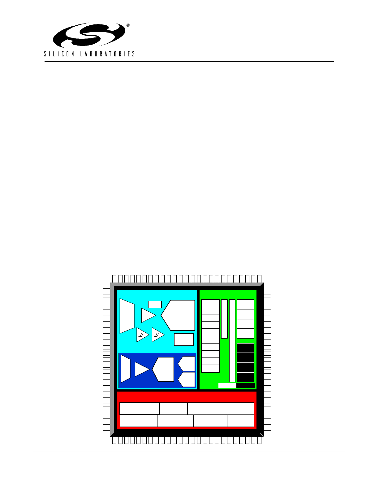
1. System Overview
The C8051F12x and C8051F13x device families are fully integrated mixed-signal System-on-a-Chip
MCUs with 64 digital I/O pins (100-pin TQFP) or 32 digital I/O pins (64-pin TQFP).
Highlighted features are listed below. Refer to Table 1.1 for specific product feature selection.
• High-Speed pipelined 8051-compatible CIP-51 microcontroller core (100 MIPS or 50 MIPS)
• In-system, full-speed, non-intrusive debug interface (on-chip)
• True 12 or 10-bit 100 ksps ADC with PGA and 8-channel analog multiplexer
• True 8-bit 500 ksps ADC with PGA and 8-channel analog multiplexer (C8051F12x Family)
• Two 12-bit DACs with programmable update scheduling (C8051F12x Family)
• 2-cycle 16 by 16 Multiply and Accumulate Engine (C8051F120/1/2/3 and C8051F130/1/2/3)
• 128 or 64 kB of in-system programmable Flash memory
• 8448 (8 k + 256) bytes of on-chip RAM
• External Data Memory Interface with 64 kB address space
• SPI, SMBus/I2C, and (2) UART serial interfaces implemented in hardware
• Five general purpose 16-bit Timers
• Programmable Counter/Timer Array with 6 capture/compare modules
• On-chip Watchdog Timer, V
Monitor, and Temperature Sensor
DD
With on-chip V
are truly stand-alone System-on-a-Ch ip solutions. All analog and digital peripherals are enabled/disabled
and configured by user firmware. The Flash memory can be reprogrammed even in-circuit, providing nonvolatile data storage, and also allowing field upgrades of the 8051 firmware.
On-board JTAG debug circuitry allows non-intrusive (uses no on-chip resources), full speed, in-circuit
debugging using the production MCU installed in the final application. This debug system supports inspection and modification of memory and registers, setting breakpoints, watchpoints, single stepping, run and
halt commands. All analog and digital peripherals are fully functional while debugging using JTAG.
Each MCU is specified for operation over the industrial temperature range (–45 to +85 °C). The Port I/O,
RST
, and JTAG pins are tolerant for input signals up to 5 V. The devices are available in 100-pin TQFP or
64-pin TQFP packaging. Table 1.1 lists the specific device features and package offerings for each part
number. Figure 1.1 through Figure 1.6 show functional block diagrams for each device.
monitor, Watchdog Timer, and clock oscillator, the C8051F12x and C8051F13x devices
DD
Rev. 1.4 19
C8051F120/1/2/3/4/5/6/7
C8051F130/1/2/3
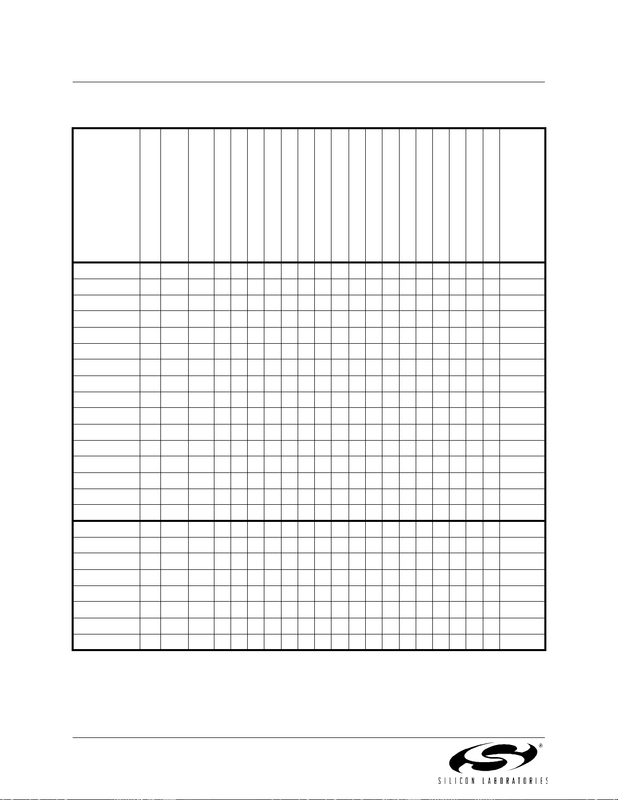
Table 1.1. Product Selection Guide
Ordering Part Number
C8051F120 100 128 k 8448
C8051F120-GQ 100 128 k 8448
C8051F121 100 128 k 8448
C8051F121-GQ 100 128 k 8448
C8051F122 100 128 k 8448
C8051F122-GQ 100 128 k 8448
C8051F123 100 128 k 8448
C8051F123-GQ 100 128 k 8448
C8051F124 50 128 k 8448 C8051F124-GQ 50 128 k 8448 C8051F125 50 128 k 8448 C8051F125-GQ 50 128 k 8448 C8051F126 50 128 k 8448 C8051F126-GQ 50 128 k 8448 C8051F127 50 128 k 8448 C8051F127-GQ 50 128 k 8448 C8051F130 100 128 k 8448
C8051F130-GQ 100 128 k 8448
C8051F131 100 128 k 8448
C8051F131-GQ 100 128 k 8448
C8051F132 100 64 k 8448
C8051F132-GQ 100 64 k 8448
C8051F133 100 64 k 8448
C8051F133-GQ 100 64 k 8448
MIPS (Peak)
Flash Memory
RAM
2-cycle 16 by 16 MAC
External Memory Interface
SMBus/I2C
SPI
UARTS
3333
3333
3333
3333
3333
3333
3333
3333
333
333
333
333
333
333
333
333
3333
3333
3333
3333
3333
3333
3333
3333
25364 8 - 8
25364 8 - 8
25332 8 - 8
25332 8 - 8
25364 - 8 8
25364 - 8 8
25332 - 8 8
25332 - 8 8
25364 8 - 8
25364 8 - 8
25332 8 - 8
25332 8 - 8
25364 - 8 8
25364 - 8 8
25332 - 8 8
25332 - 8 8
25364 - 8 25364 - 8 25332 - 8 25332 - 8 25364 - 8 25364 - 8 25332 - 8 25332 - 8 -
Timers (16-bit)
Programmable Counter Array
Digital Port I/O’s
12-bit 100ksps ADC Inputs
10-bit 100ksps ADC Inputs
8-bit 500ksps ADC Inputs
Voltage Reference
Temperature Sensor
DAC Resolution (bits)
DAC Outputs
Analog Comparators
33
33
33
33
33
33
33
33
33
33
33
33
33
33
33
33
33
33
33
33
33
33
33
33
Lead-Free (RoHS Compliant)
12 2 2 - 100TQFP
12 2 2
12 2 2 - 64TQFP
12 2 2
12 2 2 - 100TQFP
12 2 2
12 2 2 - 64TQFP
12 2 2
12 2 2 - 100TQFP
12 2 2
12 2 2 - 64TQFP
12 2 2
12 2 2 - 100TQFP
12 2 2
12 2 2 - 64TQFP
12 2 2
- - 2 - 100TQFP
--23100TQFP
- - 2 - 64TQFP
--2364TQFP
- - 2 - 100TQFP
--23100TQFP
- - 2 - 64TQFP
--2364TQFP
3
3
3
3
3
3
3
3
Package
100TQFP
64TQFP
100TQFP
64TQFP
100TQFP
64TQFP
100TQFP
64TQFP
20 Rev. 1.4

C8051F120/1/2/3/4/5/6/7
C8051F130/1/2/3
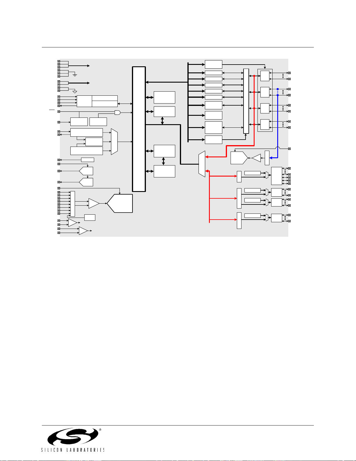
VDD
VDD
VDD
DGND
DGND
DGND
AV+
AV+
AGND
AGND
TCK
TMS
TDO
RST
MONEN
XTAL1
XTAL2
VREF
VREFD
DAC1
DAC0
VREF0
AIN0.0
AIN0.1
AIN0.2
AIN0.3
AIN0.4
AIN0.5
AIN0.6
AIN0.7
CP0+
CP0-
CP1+
CP1-
Port I/O
Digital Power
SFR Bus
Analog Power
8
Boundary Scan
TDI
JTAG
Logic
VDD
Monitor
External Oscillator
Circuit
Circuitry
Calibrated Internal
Oscillator
VREF
DAC1
(12-Bit)
DAC0
(12-Bit)
A
M
U
X
TEMP
SENSOR
CP0
CP1
Prog
Gain
PLL
Debug HW
WDT
System
Clock
100 ksps
(12-Bit)
Reset
ADC
0
5
1
C
o
r
e
256 byte
RAM
8 kB
XRAM
External D a ta
Memory Bus
128 kB
FLASH
64x4 byte
cache
Config.
UART0
UART1
SMBus
SPI Bus
PCA
Timers 0,
1, 2, 4
Timer 3/
RTC
P0, P1,
P2, P3
Latches
Crossbar
Config.
Bus Control
Address Bus
Data Bus
ADC
500 ksps
(8-Bit)
C
T
L
A
d
d
r
D
a
t
a
C
R
O
S
S
B
A
R
P4 Latch
P5 Latch
P6 Latch
P7 Latch
P0
Drv
P1
Drv
P2
Drv
P3
Drv
A
8:1
M
Prog
Gain
U
X
P4
DRV
P5
DRV
P6
DRV
P7
DRV
P0.0
P0.7
P1.0/AIN2.0
P1.7/AIN2.7
P2.0
P2.7
P3.0
P3.7
VREF2
P4.0
P4.4
P4.5/ALE
P4.6/RD
P4.7/WR
P5.0/A8
P5.7/A15
P6.0/A0
P6.7/A7
P7.0/D0
P7.7/D7
Figure 1.1. C8051F120/124 Block Diagram
Rev. 1.4 21

C8051F120/1/2/3/4/5/6/7
C8051F130/1/2/3
VDD
VDD
VDD
DGND
DGND
DGND
AV+
AGND
TCK
TMS
TDO
RST
MONEN
XTAL1
XTAL2
VREF
DAC1
DAC0
VREFA
AIN0.0
AIN0.1
AIN0.2
AIN0.3
AIN0.4
AIN0.5
AIN0.6
AIN0.7
CP0+
CP0CP1+
CP1-
Port I/O
Digital Power
SFR Bus
Analog Power
Boundary Scan
TDI
JTAG
Logic
VDD
Monitor
External Oscillator
Circuit
Circuitry
Calibrated Internal
Oscillator
VREF
DAC1
(12-Bit)
DAC0
(12-Bit)
A
M
U
X
TEMP
SENSOR
CP0
CP1
Prog
Gain
PLL
Debug HW
WDT
System
Clock
100 ksps
(12-Bit)
Reset
ADC
8
0
5
1
C
o
r
e
256 byte
RAM
8 kB
XRAM
External Data
Memory Bus
128 kB
FLASH
64x4 byte
cache
Config.
UART0
UART1
SMBus
SPI Bus
PCA
Timers 0,
1, 2, 4
Timer 3/
RTC
P0, P1,
P2, P3
Latches
Crossbar
Config.
Bus Control
Address Bus
Data Bus
ADC
500 ksps
(8-Bit)
C
T
L
A
d
d
r
D
a
t
a
C
R
O
S
S
B
A
R
P4 Latch
P5 Latch
P6 Latch
P7 Latch
AV+
VREFA
P0
Drv
P1
Drv
P2
Drv
P3
Drv
A
8:1
M
Prog
Gain
U
X
P4
DRV
P5
DRV
P6
DRV
P7
DRV
P0.0
P0.7
P1.0/AIN2.0
P1.7/AIN2.7
P2.0
P2.7
P3.0
P3.7
Figure 1.2. C8051F121/125 Block Diagram
22 Rev. 1.4
C8051F120/1/2/3/4/5/6/7
C8051F130/1/2/3
VDD
VDD
VDD
DGND
DGND
DGND
AV+
AV+
AGND
AGND
TCK
TMS
TDO
RST
MONEN
XTAL1
XTAL2
VREF
VREFD
DAC1
DAC0
VREF0
AIN0.0
AIN0.1
AIN0.2
AIN0.3
AIN0.4
AIN0.5
AIN0.6
AIN0.7
CP0+
CP0-
CP1+
CP1-
Port I/O
Digital Power
SFR Bus
Analog Power
8
Boundary Scan
TDI
JTAG
Logic
VDD
Monitor
Externa l Oscillator
Circuit
Circuitry
Calibrated Internal
Oscillator
VREF
DAC1
(12-Bit)
DAC0
(12-Bit)
A
M
U
X
TEMP
SENSOR
CP0
CP1
Prog
Gain
PLL
Debug HW
WDT
System
Clock
100 ksps
(10-Bit)
Reset
ADC
0
5
1
C
o
r
e
256 byte
RAM
8 kB
XRAM
External D a ta
Memory Bus
128 kB
FLASH
64x4 byte
cache
Config.
UART0
UART1
SMBus
SPI Bus
PCA
Timers 0,
1, 2, 4
Timer 3/
RTC
P0, P1,
P2, P3
Latches
Crossbar
Config.
Bus Control
Address Bus
Data Bus
ADC
500 ksps
(8-Bit)
C
T
L
A
d
d
r
D
a
t
a
C
R
O
S
S
B
A
R
P4 Latch
P5 Latch
P6 Latch
P7 Latch
P0
Drv
P1
Drv
P2
Drv
P3
Drv
A
8:1
M
Prog
Gain
U
X
P4
DRV
P5
DRV
P6
DRV
P7
DRV
P0.0
P0.7
P1.0/AIN2.0
P1.7/AIN2.7
P2.0
P2.7
P3.0
P3.7
VREF2
P4.0
P4.4
P4.5/ALE
P4.6/RD
P4.7/WR
P5.0/A8
P5.7/A15
P6.0/A0
P6.7/A7
P7.0/D0
P7.7/D7
Figure 1.3. C8051F122/126 Block Diagram
Rev. 1.4 23
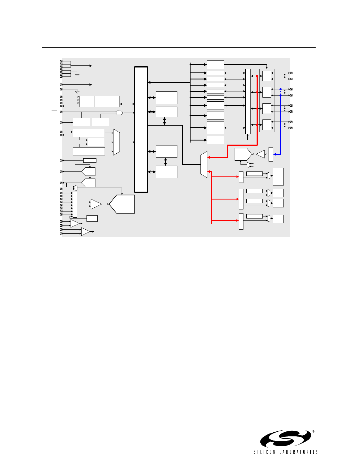
C8051F120/1/2/3/4/5/6/7
C8051F130/1/2/3
VDD
VDD
VDD
DGND
DGND
DGND
AV+
AGND
TCK
TMS
TDO
RST
MONEN
XTAL1
XTAL2
VREF
DAC1
DAC0
VREFA
AIN0.0
AIN0.1
AIN0.2
AIN0.3
AIN0.4
AIN0.5
AIN0.6
AIN0.7
CP0+
CP0-
CP1+
CP1-
Port I/O
Digital Power
SFR Bus
Analog Power
Boundary Scan
TDI
JTAG
Logic
VDD
Monitor
External Oscillator
Circuit
Circuitry
Calibrated Internal
Oscillator
VREF
DAC1
(12-Bit)
DAC0
(12-Bit)
A
M
U
X
TEMP
SENSOR
CP0
CP1
Prog
Gain
PLL
Debug HW
WDT
System
Clock
100 ksps
(10-Bit)
Reset
ADC
8
0
5
1
C
o
r
e
256 byte
RAM
8 kb
XRAM
External Data
Memory Bus
128 kb
FLASH
64x4 byte
cache
Config.
UART0
UART1
SMBus
SPI Bus
PCA
Timers 0,
1, 2, 4
Timer 3/
RTC
P0, P1,
P2, P3
Latches
Crossbar
Config.
Bus Control
Address Bus
Data Bus
ADC
500 ksps
(8-Bit)
C
T
L
A
d
d
r
D
a
t
a
C
R
O
S
S
B
A
R
P4 Latch
P5 Latch
P6 Latch
P7 Latch
AV+
VREFA
P0
Drv
P1
Drv
P2
Drv
P3
Drv
A
8:1
M
Prog
Gain
U
X
P4
DRV
P5
DRV
P6
DRV
P7
DRV
P0.0
P0.7
P1.0/AIN2.0
P1.7/AIN2.7
P2.0
P2.7
P3.0
P3.7
Figure 1.4. C8051F123/127 Block Diagram
24 Rev. 1.4
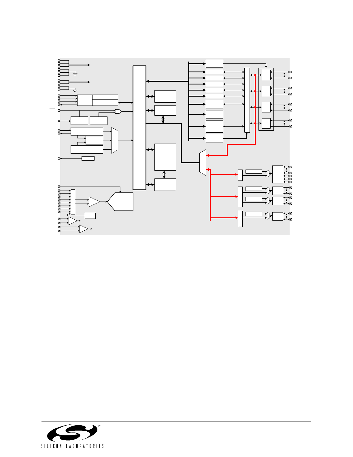
C8051F120/1/2/3/4/5/6/7
C8051F130/1/2/3
VDD
VDD
VDD
DGND
DGND
DGND
AV+
AV+
AGND
AGND
TCK
TMS
TDO
RST
MONEN
XTAL1
XTAL2
VREF
VREF0
AIN0.0
AIN0.1
AIN0.2
AIN0.3
AIN0.4
AIN0.5
AIN0.6
AIN0.7
CP0+
CP0-
CP1+
CP1-
Port I/O
Digital Power
SFR Bus
Analog Power
8
Boundary Scan
TDI
JTAG
Logic
VDD
Monitor
External Oscillator
Calibrated Inte rn al
Circuit
Circuitry
Oscillator
VREF
WDT
PLL
Debug HW
System
Clock
Reset
0
5
1
C
o
r
e
ADC
100ksps
(10-Bit)
CP0
A
M
U
X
CP1
TEMP
SENSOR
Prog
Gain
256 byte
RAM
8kbyte
XRAM
External D ata
Memory Bus
FLASH
128kbyte
(‘F130)
64kbyte
(‘F132)
64x4 byte
cache
Config.
UART0
UART1
SMBus
SPI Bus
PCA
Timers 0,
1, 2, 4
Timer 3/
RTC
P0, P1,
P2, P3
Latches
Crossbar
Config.
Bus Control
Address Bus
Data Bus
C
T
L
A
d
d
D
a
a
r
t
C
R
O
S
S
B
A
R
P4 Latch
P5 Latch
P6 Latch
P7 Latch
P0
Drv
P1
Drv
P2
Drv
P3
Drv
P4
DRV
P5
DRV
P6
DRV
P7
DRV
P0.0
P0.7
P1.0/AIN2.0
P1.7/AIN2.7
P2.0
P2.7
P3.0
P3.7
P4.0
P4.4
P4.5/ALE
P4.6/RD
P4.7/WR
P5.0/A8
P5.7/A15
P6.0/A0
P6.7/A7
P7.0/D0
P7.7/D7
Figure 1.5. C8051F130/132 Block Diagram
Rev. 1.4 25
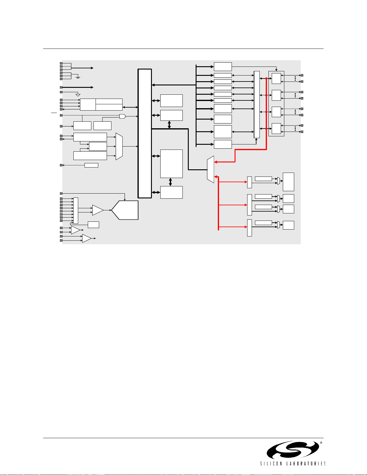
C8051F120/1/2/3/4/5/6/7
C8051F130/1/2/3
VDD
VDD
VDD
DGND
DGND
DGND
AV+
AGND
TCK
TMS
TDO
RST
MONEN
XTAL1
XTAL2
VREF
VREF0
AIN0.0
AIN0.1
AIN0.2
AIN0.3
AIN0.4
AIN0.5
AIN0.6
AIN0.7
CP0+
CP0-
CP1+
CP1-
Port I/O
Digital Power
SFR Bus
Analog Power
Boundary Scan
TDI
JTAG
Logic
VDD
Monitor
External Oscillator
Circuit
Circuitry
Calibrated Inte rn al
Oscillator
VREF
CP0
A
M
U
X
CP1
TEMP
SENSOR
Prog
Gain
Debug HW
WDT
PLL
System
Clock
100ksps
(10-Bit)
Reset
ADC
8
0
5
1
C
o
r
e
256 byte
RAM
8kbyte
XRAM
External D ata
Memory Bus
FLASH
128kbyte
(‘F131)
64kbyte
(‘F133)
64x4 byte
cache
Config.
UART0
UART1
SMBus
SPI Bus
PCA
Timers 0,
1, 2, 4
Timer 3/
RTC
P0, P1,
P2, P3
Latches
Crossbar
Config.
Bus Control
Address Bus
Data Bus
C
T
L
A
d
d
D
a
a
r
t
C
R
O
S
S
B
A
R
P4 Latch
P5 Latch
P6 Latch
P7 Latch
P0
Drv
P1
Drv
P2
Drv
P3
Drv
P4
DRV
P5
DRV
P6
DRV
P7
DRV
P0.0
P0.7
P1.0/AIN2.0
P1.7/AIN2.7
P2.0
P2.7
P3.0
P3.7
Figure 1.6. C8051F131/133 Block Diagram
26 Rev. 1.4

C8051F120/1/2/3/4/5/6/7
C8051F130/1/2/3
1.1. CIP-51™ Microcontroller Core
1.1.1. Fully 8051 Compatible
The C8051F12x and C8051F13x utilize Silicon Labs’ proprietary CIP-51 microcontroller core. The CIP-51
is fully compatible with the MCS-51™ instruction set; standard 803x/805x assemblers and compilers can
be used to develop software. The core has all the periphera l s include d with a standard 8052, including five
16-bit counter/timers, two full-duplex UARTs, 256 bytes of internal RAM, 128 byte Special Function Register (SFR) address space, and 8/4 byte-wide I/O Ports.
1.1.2. Improved Throughput
The CIP-51 employs a pipelined architectu re that grea tly increases its instruction throughput over the st andard 8051 architecture. In a standard 8051, all instructions except for MUL and DIV take 12 or 24 system
clock cycles to execute with a maximum system clock of 12-to-24 MHz. By contrast, the CIP-51 core executes 70% of its instructions in one or two system clock cycles, with only four instructions taking more than
four system clock cycles.
The CIP-51 has a total of 109 instructions. The table below shows the total number of instructions that
require each execution time.
Clocks to Execute 1 22/333/444/55 8
Number of Instructions 26 50 5 14 7 3 1 2 1
With the CIP-51's maximum system clock at 100 MHz, the C8051F120/1/2/3 and C8051F130/1/2/3 have a
peak throughput of 100 MIPS (the C8051F124/5/6/7 have a peak throughput of 50 MIPS).
Rev. 1.4 27
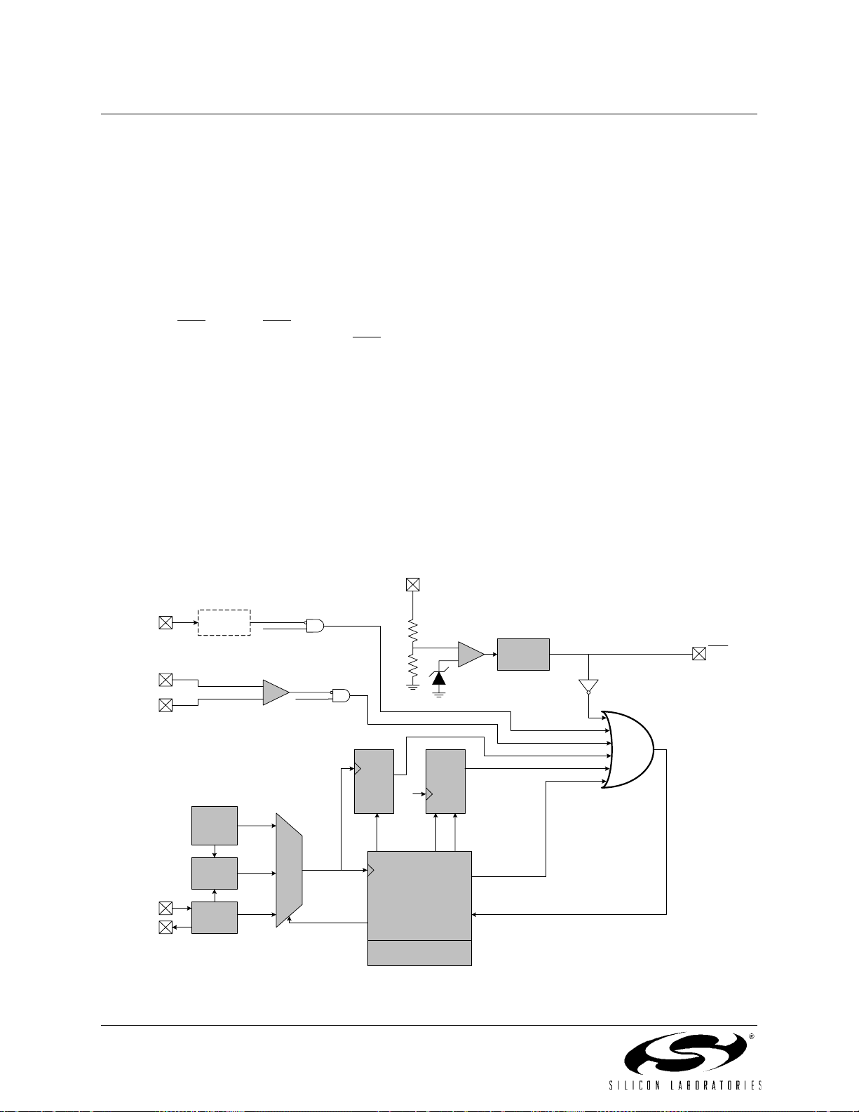
C8051F120/1/2/3/4/5/6/7
C8051F130/1/2/3
1.1.3. Additional Features
Several key enhancements are implemented in the CIP-51 core and peripherals to improve overall performance and ease of use in end applications.
The extended interrupt handler provides 20 interrupt sources into the CIP-51 (as opposed to 7 for the standard 8051), allowing the numerous analog and digital peripherals to interrupt the controller. An interrupt
driven system requires less intervention by the MCU, giving it more effective throughput. The extra interrupt sources are very useful when building multi-tasking, real-time systems.
There are up to seven reset sources for the MCU: an on-board V
monitor, a Watchdog Timer, a missing
DD
clock detector, a voltage level detection from Comparator0, a forced software reset, the CNVSTR0 input
pin, and the RST
nally generated POR to be output on the RST
Input pin may be disabled by the user in software; the V
pin. The RST pin is bi-directional, accommodating an external rese t, or allowing the inter-
pin. Each reset source except for the VDD monitor and Reset
monitor is enabled/disabled via th e MONEN
DD
pin. The Watchdog Timer may be permanently enabled in software after a power-on reset during MCU initialization.
The MCU has an internal, stand alone clock generator which is used by default as the system clock after
any reset. If desired, the clock source may be switched on the fly to the external oscillator , which can use a
crystal, ceramic resonator, capacitor, RC, or external clock source to generate the system clock. This can
be extremely useful in low power applications, allowing the MCU to run from a slow (power saving) external crystal source, while periodically switching to the 24.5 MH z internal oscillator as needed. Additionally,
an on-chip PLL is provided to achieve higher system clock speeds for increased throughput.
V
DD
(Port I/O)
CP0+
CP0-
XTAL1
XTAL2
Crossbar
Internal
Clock
Generator
PLL
Circuitry
OSC
CNVSTR
(CNVSTR
reset
enable)
Comparator0
+
-
(CP0
reset
enable)
System
Clock
Clock Select
Missing
Clock
Detector
(one-
shot)
EN
Enable
WDT
Enable
MCD
CIP-51
Microcontroller
Core
Extended Interrupt
Handler
EN
WDT
Supply
Monitor
+
-
PRE
WDT
Supply
Reset
Timeout
Strobe
Software Reset
System Reset
(wired-OR)
Reset
Funnel
RST
Figure 1.7. On-Board Clock and Reset
28 Rev. 1.4
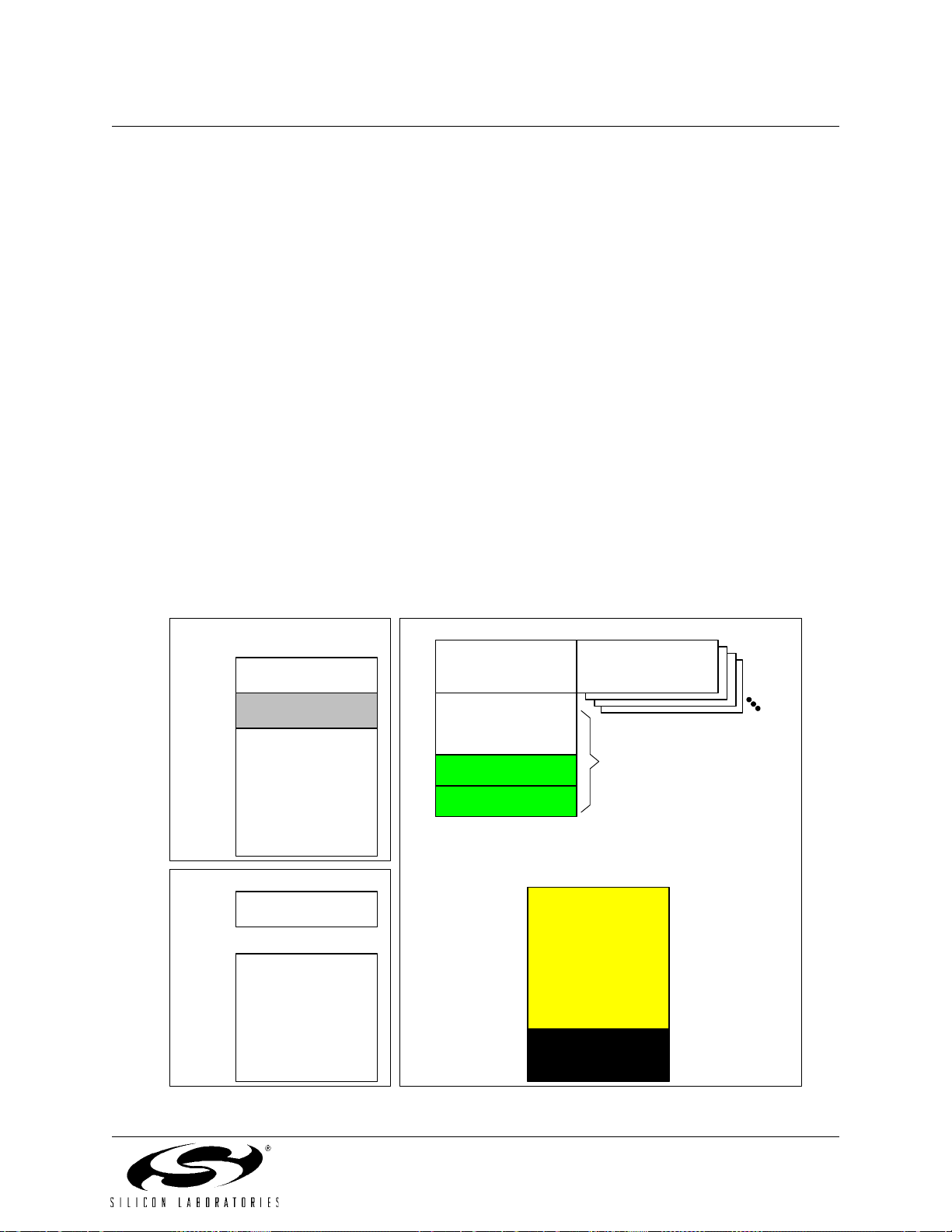
C8051F120/1/2/3/4/5/6/7
C8051F130/1/2/3
1.2. On-Chip Memory
The CIP-51 has a standard 8051 program and data address configuration. It includes 256 bytes of data
RAM, with the upper 128 bytes dual-mapped. Indirect addressing accesses the upper 128 bytes of general
purpose RAM, and direct addressing accesses the 128 byte SFR address space. The lower 128 bytes of
RAM are accessible via direct and indirect addressing. The first 32 bytes are addressable as four banks of
general purpose registers, and the next 16 bytes can be byte addressable or bit addressable.
The devices include an on-chip 8k byte RAM block and an external memory interf ace (EM IF) for acce ssing
off-chip data memory. The on-chip 8k byte block can be addressed over the entire 64k external data memory address range (overlapping 8k boundaries). External data memory address space can be mapped to
on-chip memory only, off-chip memor y only, or a combination of the two (addresses up to 8k directed to onchip, above 8k directed to EMIF). The EMIF is also configurable for multiplexed or non-multiplexed
address/data lines.
On the C8051F12x and C8051F130/1, the MCU’s program memory consists of 128 k bytes of banked
Flash memory. The 1024 bytes from addresses 0x1FC00 to 0x1FFFF are reserved. On the C8051F132/3,
the MCU’s program memory consists of 64 k bytes of Flash memory. This memory may be reprogrammed
in-system in 1024 byte sectors, and requires no special off-chip programming voltage.
On all devices, there are also two 128 byte sectors at addresses 0x20000 to 0x200FF, which may be used
by software for data storage. See Figure 1.8 for the MCU system memory map.
PROGRAM/DATA MEMORY
(FLASH)
C8051F120/1/2/3/4/5/6/7
C8051F130/1
0x200FF
0x20000
0x1FFFF
0x1FC00
0x1FBFF
0x00000
Scrachpad Memory
(DATA only)
RESERVED
FLASH
(In-System
Programmable in 1024
Byte Sectors)
C8051F132/3
0x200FF
0x20000
0x0FFFF
0x00000
Scrachpad Memory
(DATA only)
FLASH
(In-System
Programmable in 1024
Byte Sectors)
DATA MEMORY (RAM)
INTERNAL DATA ADDRESS SPACE
Upper 128 RAM
(Indirect Addressing
Only)
(Direct and Indirect
Addressing)
Bit Addressable
General Purpose
Registers
Special Function
Registers
(Direct Addressing Only)
Lower 128 RAM
(Direct and Indirect
Addressing)
EXTERNAL DATA ADDRESS SPACE
0xFFFF
Off-chip XRAM space
0x2000
0x1FFF
0x0000
XRAM - 8192 Bytes
(accessable using MOVX
instruction)
0
1
2
3
Up To
256 SFR Pages
Figure 1.8. On-Chip Memory Map
Rev. 1.4 29
C8051F120/1/2/3/4/5/6/7
C8051F130/1/2/3
1.3. JTAG Debug and Boundary Scan
JTAG boundary scan and debug circuitry is included which provides non-intrusive, full speed, in-circuit
debugging using the production part installed in the end application, via the four-pin JTAG interface. The
JTAG port is fully compliant to IEEE 1149.1, providing full boundary scan for test and manufacturing purposes.
Silicon Labs' debugging system supports inspection and modification of memory and registers, breakpoints, watchpoints, a stack monitor, and single stepping. No additional target RAM, program memory, timers, or communications channels are required. All the digital and analog peripherals are functional and
work correctly while debugging. All the peripherals (except for the ADC and SMBus) are stalled when the
MCU is halted, during single stepping, or at a breakpoint in order to keep them synchronized.
The C8051F120DK development kit provides all the hardware and software necessary to develop application code and perform in-circuit debugging with the C8051F12x or C8051F13x MCUs.
The kit includes a Windows (95 or later) development environment, a serial adapter for connecting to the
JTAG port, and a target application board with a C8051F120 MCU installed. All of the necessary communication cables and a wall-mount power supply are also supplied with the development kit. Silicon Labs’
debug environment is a vastly superior configuration for de veloping and debugging embedd ed applications
compared to standard MCU emulators, which use on-board "ICE Chips" and target cables and require the
MCU in the application board to be socketed. Silicon Labs' debug environment both increases ease of use
and preserves the performance of the precision, on-chip analog peripherals.
WINDOWS 95 OR LATE R
Figure 1.9. Development/In-System Debug Diagram
Silicon Labs Integrated
Development Environment
JTA G (x 4 ), V DD, G ND
Serial
Adapter
TARGET PCB
C8051
F12x/13x
30 Rev. 1.4
C8051F120/1/2/3/4/5/6/7
C8051F130/1/2/3
1.4. 16 x 16 MAC (Multiply and Accumulate) Engine
The C8051F120/1/2/3 and C8051F130/1/2/3 devices include a multiply and accumulate engine which can
be used to speed up many mathematical operations. MAC0 contains a 16-by-16 bit multiplier and a 40-bit
adder, which can perform integer or fractional multiply-accumulate and multiply operations on signed input
values in two SYSCLK cycles. A rounding engine provides a rounded 16-bit fractional result after an additional (third) SYSCLK cycle. MAC0 also contains a 1-bit arithmetic shifter that will left or right-shift the contents of the 40-bit accumulator in a single SYSCLK cycle.
MAC0 A Register
MAC0AH MAC0AL
MAC0FM
16 x 1 6 M u ltip ly
MAC0 B Register
MAC0BH MAC0BL
MAC0MS
1
0
0
40 bit Add
MAC0 Accumulator
MAC0OVR MAC0ACC3 MAC0ACC2 MAC0ACC1 MAC0ACC0
Rounding Engine1 bit Shift
Flag Logic
MAC0 Rounding Register
MAC0RNDH MAC0RNDL
MAC0MS
MAC0FM
MAC0SAT
MAC0CA
MAC0SD
MAC0SC
MAC0CF
MAC0STA
MAC0HO
MAC0SO
MAC0Z
MAC0N
Figure 1.10. MAC0 Block Diagram
Rev. 1.4 31

C8051F120/1/2/3/4/5/6/7
C8051F130/1/2/3
1.5. Programmable Digital I/O and Crossbar
The standard 8051 8-bit Ports (0, 1, 2, and 3) are available on the MCUs. The devices in the larger (100pin TQFP) packaging have 4 additional ports (4, 5, 6, and 7) for a total of 64 general-purpose port I/O. The
Port I/O behave like the standard 8051 with a few enhancements.
Each Port I/O pin can be configured as either a push-pull or open-drain output. Also, the "weak pullups"
which are normally fixed on an 8051 can be globally disabled, providing additional power saving capabilities for low-power applications.
Perhaps the most unique enhancement is the Digital Cr ossbar. This is a large digital switching network that
allows mapping of internal digital system resources to Port I/O pins on P0, P1, P2, and P3. (See
Figure 1.11) Unlike microcontrollers with standard multiplexed digital I/O, all combinations of functions are
supported.
The on-chip counter/timers, serial buses, HW interrupts, ADC Start of Conversion inputs, comparator outputs, and other digital signals in the controller can be configured to app ear on the Port I/O pins specified in
the Crossbar Control registers. This allows the user to select the exact mix of general purpose Port I/O and
digital resources needed for the particular application.
Highest
Priority
Lowest
Priority
Port
Latches
UART0
SPI
SMBus
UART1
PCA
Comptr.
Outputs
(Internal Digital Signals)
T0, T1,
T2, T2EX,
T4,T4EX
/INT0,
/INT1
/SYSCLK divided by 1,2,4, or 8
CNVSTR0/2
8
P0
(P0.0-P0.7)
8
P1
(P1.0-P1.7)
8
P2
(P2.0-P2.7)
8
P3
(P3.0-P3.7)
2
4
2
XBR0, XBR1,
XBR2, P1MDIN
Registers
Priority
2
7
2
Decoder
Digital
Crossbar
8
2
To Extern a l
Memory
Interface
(EMIF)
P0MDOUT, P1MDOUT,
P2MDOUT, P3MDOUT
Registers
8
8
8
8
P0
I/O
Cells
P1
I/O
Cells
P2
I/O
Cells
P3
I/O
Cells
To ADC2 Input
(‘F12x Only)
External
Pins
P0.0
P0.7
P1.0
P1.7
P2.0
P2.7
P3.0
P3.7
Highest
Priority
Lowest
Priority
Figure 1.11. Digital Crossbar Diagram
32 Rev. 1.4

C8051F120/1/2/3/4/5/6/7
C8051F130/1/2/3
1.6. Programmable Counter Array
An on-board Programmable Counter/Timer Array (PCA) is included in addition to the five 16-bit general
purpose counter/timers. The PCA consists of a dedicated 16-bit counter/timer time base with 6 programmable capture/compare modules. The timebase is clocked from one of six sources: the system clock
divided by 12, the system clo ck divided by 4, Timer 0 overflo w, an External Clock Input (ECI pin), th e system clock, or the external oscillator source divided by 8.
Each capture/compare module can be configured to operate in one of six modes: Edge-Triggered Capture,
Software Time r, High Speed Output, Frequency Output, 8-Bit Pulse Width Modulator, or 16-Bit Pulse Width
Modulator. The PCA Capture/Compare Module I/O and External Clock Input are routed to the MCU Port I/
O via the Digital Crossbar.
SYSCLK/12
SYSCLK/4
Timer 0 Overflow
ECI
SYSCLK
External Clock/8
PCA
CLOCK
MUX
16-Bit Counter/Timer
Capture/Compare
Module 1
CEX1
Capture/Compare
Module 2
CEX2
Capture/Compare
Module 3
CEX3
Capture/Compare
Module 4
CEX4
Capture/Compare
Module 5
CEX5
ECI
Capture/Compare
Module 0
CEX0
Crossbar
Port I/O
Figure 1.12. PCA Block Diagram
1.7. Serial Ports
Serial peripherals included on the devices are two Enhanced Full-Duplex UARTs, SPI Bus, and SMBus/
I2C. Each of the serial buses is fully implemented in hardware and makes extensive use of the CIP-51's
interrupts, thus requiring very little intervention by the CPU. The serial buses do not "share" resources
such as timers, interrupts, or Port I/O, so any or all of the serial buses may be used tog ether with any other.
Rev. 1.4 33

C8051F120/1/2/3/4/5/6/7
C8051F130/1/2/3
1.8. 12 or 10-Bit Analog to Digital Converter
All devices include either a 12 or 10-bit SAR ADC (ADC0) with a 9-channel input multiplexer and programmable gain amplifier . With a maximum thr oug hput of 100 ksps, the 12 and 10-bit ADCs offe r tru e 12-b it linearity with an INL of ±1LSB. The ADC0 voltage reference can be selected from an external VREF pin, or
(on the C8051F12x devices) the DAC0 output. On the 100-pin TQFP devices, ADC0 has it s own dedicate d
Voltage Reference input pin; on the 64-pin TQFP devices, the ADC0 shares a Voltage Reference input pin
with the 8-bit ADC2. The on-chip voltage reference may generate the voltage reference for other system
components or the on-chip ADCs via the VREF output pin.
The ADC is under full control of the CIP-51 microcontroller via its associated Special Function Registers.
One input channel is tied to an internal temperature sensor, while the other eight channels are available
externally. Each pair of the eight external input channels can be configured as either two single-ended
inputs or a single differential input. The system controller can also put the ADC into shutdown mode to
save power.
A programmable gain amplifier follows the analog multiplexer. The gain can be set in software from 0.5 to
16 in powers of 2. The gain stage can be especially useful when different ADC input channels have widely
varied input voltage signals, or when it is necessary to "zoom in" on a signal with a large DC offset (in differential mode, a DAC could be used to provide the DC offset).
Conversions can be started in four ways; a software command, an overflow of Timer 2, an overflow of
Timer 3, or an external signal input. This flexibility allows the start of conversion to be triggered by sof tware
events, external HW signals, or a periodic timer overflow signal. Conversion completions are indicated by a
status bit and an interrupt (if enabled). The resulting 10 or 12-bit data word is latched into two SFRs upon
completion of a conversion. The data can be right or left justified in these registers under software control.
Window Compare registers for the ADC data can be configured to interrupt the controller when ADC data
is within or outside of a specified range. The ADC can monitor a key voltage continuously in backgr ound
mode, but not interrupt the controller unless the converted data is within the specified window.
34 Rev. 1.4
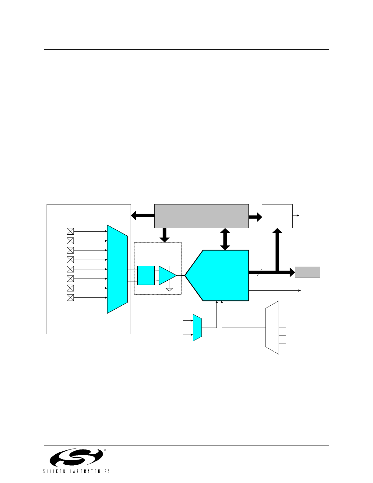
C8051F120/1/2/3/4/5/6/7
C8051F130/1/2/3
1.9. 8-Bit Analog to Digital Converter
The C8051F12x devices have an on-board 8-bit SAR ADC (ADC2) with an 8-channel inp ut multiplexer and
programmable gain amplifier. This ADC features a 500 ksps maximum throughput and true 8-bit linearity
with an INL of ±1LSB. Eight input pins are available for measurement. The ADC is under full control of the
CIP-51 microcontroller via the Special Function Registers. The ADC2 voltage reference is selected
between the analog power supply (AV+) and an external VREF pin. On the 100-pin TQFP devices, ADC2
has its own dedicated Voltage Reference input pin; on the 64-pin TQFP devices, ADC2 shares a Voltage
Reference input pin with ADC0. User software may put ADC2 into shutdown mode to save power.
A programmable gain amplifier follows the analog multiplexer. The gain stage can be especially useful
when different ADC input channels have widely varied inp ut voltage signals, or when it is necessary to
"zoom in" on a signal with a large DC offset (in differential mode, a DAC could be used to provide the DC
offset). The PGA gain can be set in software to 0.5, 1, 2, or 4.
A flexible conversion scheduling system allows ADC2 conversions to be initiated by software commands,
timer overflows, or an external input signal. ADC 2 conver sions may also be synchro nized with ADC0 software-commanded conversions. Conversion completions are indicated by a status bit and an interrupt (if
enabled), and the resulting 8-bit data word is latched into an SFR upon completion.
AIN2.0
AIN2.1
AIN2.2
AIN2.3
AIN2.4
AIN2.5
AIN2.6
AIN2.7
Analo g Multiple xer
8-to-1
AMUX
Configuration, Control, and Data Registers
Programmable Gain
Amp lifie r
AV+
+
X
-
8-Bit
SAR
ADC
8
Window
Compare
Logic
Window
Compare
Interrup t
ADC Data
Register
Conversion
Complete
Interrupt
External VREF
Pin
AV+
VREF
Start Conversion
Figure 1.14. 8-Bit ADC Diagram
Rev. 1.4 35
Write to AD2BUSY
Timer 3 Overflow
CNVSTR2 Input
Timer 2 Overflow
Write to AD0BUSY
(synchronized with
ADC0)

C8051F120/1/2/3/4/5/6/7
C8051F130/1/2/3
1.10. 12-bit Digital to Analog Converters
The C8051F12x devices have two integrated 12-bit Digital to Analog Converters (DACs). The MCU data
and control interface to each DAC is via the Special Function Registers. The MCU can place either or both
of the DACs in a low power shutdown mode.
The DACs are voltage output mode and include a flexible output scheduling mechanism. This scheduling
mechanism allows DAC output updates to be forced by a software write or scheduled on a Timer 2, 3, or 4
overflow. The DAC volt age refer ence is supplied from the dedicate d VREFD input pin on the 100-p in TQFP
devices or via the internal Voltage reference on the 64-pin TQFP devices. The DACs are especially useful
as references for the comparators or offset s for the differential inputs of the ADCs.
DAC0EN
DAC0H
Timer 3
Timer 4
Timer 2
DAC0MD1
DAC0MD0
DAC0DF2
DAC0CN
DAC0DF1
DAC0DF0
DAC0HDAC0L
8
8
8
8
Latch Latch
Dig. MUX
REF
12
AV+
DAC0
DAC0
AGND
DAC1EN
DAC1H
Timer 3
Timer 4
Timer 2
DAC1MD1
DAC1MD0
DAC1DF2
DAC1CN
DAC1DF1
DAC1DF0
8
DAC1HDAC1L
8
8
8
Latch Latch
REF
12
Dig. MUX
DAC1
Figure 1.15. DAC System Block Diagram
36 Rev. 1.4
AV+
DAC1
AGND

C8051F120/1/2/3/4/5/6/7
C8051F130/1/2/3
1.11. Analog Comparators
Two analog comparators with dedicated input pins are included on-chip. The comparators have software
programmable hysteresis and response time. Each comparator can g enera te an inte rrupt on a rising edg e,
falling edge, or both. The interrupts are capable of waking up the MCU from sleep mode, and Comparator
0 can be used as a reset source. The output st ate o f the comp ar ators can be polled in sof tware or r outed to
Port I/O pins via the Crossbar. The comp arators can b e progr ammed to a low power sh ut down mode whe n
not in use.
(Port I/O)
2 Comparators
CPn+
CPn-
CPn Output
+
CPn
-
CROSSBAR
SFR's
(Data
and
Control)
Figure 1.16. Comparator Block Diagram
CIP-51
and
Interrupt
Handler
Rev. 1.4 37

C8051F120/1/2/3/4/5/6/7
C8051F130/1/2/3
2. Absolute Maximum Ratings
Table 2.1. Absolute Maximum Ratings
Parameter Conditions Min Typ Max Units
Ambient temperature under bias
Storage Temperature
Voltage on any Pin (except V
Respect to DGND
Voltage on any Port I/O Pin or RST
DGND
Voltage on V
Maximum Total Current through V
and AGND
Maximum Output Current Sunk by any Port pin
Maximum Output Current Sunk by any other I/O pin
Maximum Output Current Sourced by any Port pin
Maximum Output Current Sourced by any other I/O
Pin
*Note: Stresses above those listed under “Absolute Maximum Ratings” may cause permanent damage to the device.
This is a stress rating only and functional operation of the devices at those or any other conditions above those
indicated in the operation listings of this specification is not implied. Exposure to maximum rating conditions for
extended periods may affect device reliability.
with Respect to DGND
DD
and Port I/O) with
DD
with Respect to
, AV+, DGND,
DD
*
–55 — 125 °C
–65 — 150 °C
–0.3 — V
–0.3 — 5.8 V
–0.3 — 4.2 V
——800mA
——100mA
—— 50mA
——100mA
—— 50mA
DD
0.3
+
V
38 Rev. 1.4

C8051F120/1/2/3/4/5/6/7
C8051F130/1/2/3
3. Global DC Electrical Characteristics
Table 3.1. Global DC Electrical Characteristics (C8051F120/1/2/3 and C8051F130/1/2/3)
–40 to +85 °C, 100 MHz System Clock unless otherwise specified.
Parameter Conditions Min Typ Max Units
Analog Supply Voltage
1
Analog Supply Current Internal REF, ADCs, DACs, Com-
Analog Supply Current with
analog sub-systems inactive
Analog-to-Digital Supply
Delta (|V
DD
–AV+|)
Digital Supply Voltage SYSCLK = 0 to 50 MHz
Digital Supply Current with
CPU active
Digital Supply Current with
CPU inactive (not accessing
Flash)
Digital Supply Current (shutdown)
Digital Supply RAM Data
Retention Voltage
SYSCLK (System Clock)
Specified Operating Temperature Range
Notes:
1.
Analog Supply AV+ must be greater than 1 V for VDD monitor to operate.
2. SYSCLK is the internal device clock. For operational speeds in excess of 30 MHz, SYSCLK must be derived
from the Phase-Locked Loop (PLL).
3. SYSCLK must be at least 32 kHz to enable debugging.
SYSCLK = 0 to 50 MHz
SYSCLK > 50 MHz
parators all active
Internal REF, ADCs, DACs, Com-
parators all disabled, oscillator
disabled
SYSCLK > 50 MHz
= 3.0 V , Clock = 100 MHz
V
DD
V
= 3.0 V , Clock = 50 MHz
DD
V
= 3.0 V, Clock = 1 MHz
DD
V
= 3.0 V, Clock = 32 kHz
DD
= 3.0 V , Clock = 100 MHz
V
DD
V
= 3.0 V , Clock = 50 MHz
DD
V
= 3.0 V, Clock = 1 MHz
DD
V
= 3.0 V, Clock = 32 kHz
DD
Oscillator not running
2,3
VDD, AV+ = 2.7 to 3.6 V
, AV+ = 3.0 to 3.6 V
V
DD
2.7
3.0
3.0
3.3
3.6
3.6
—1.7—mA
—0.2—µA
——0.5V
2.7
3.0
—65
3.0
3.3
3.6
3.6
—mA
35
1
33
—40
—mA
20
0.4
15
—0.4—µA
—1.5— V
0
0
—50
100
–40 — +85 °C
V
V
V
V
mA
mA
µA
mA
mA
µA
MHz
MHz
Rev. 1.4 39

C8051F120/1/2/3/4/5/6/7
C8051F130/1/2/3
Table 3.2. Global DC Electrical Characteristics (C8051F124/5/6/7)
–40 to +85 °C, 50 MHz System Clock unless oth erwise specified.
Parameter Conditions Min Typ Max Units
Analog Supply Voltage
1
Analog Supply Current Internal REF, ADC, DAC, Com-
parators all active
Analog Supply Current with
analog sub-systems inactive
Internal REF, ADC, DAC, Comparators all disabled, oscillator
disabled
Analog-to-Digital Supply
Delta (|V
DD
–AV+|)
Digital Supply Voltage
Digital Supply Current with
CPU active
Digital Supply Current with
CPU inactive (not accessing
Flash)
Digital Supply Current (shut-
V
=3.0V, Clock=50MHz
DD
V
= 3.0 V, Clock = 1 MHz
DD
V
=3.0V, Clock=32kHz
DD
V
=3.0V, Clock=50MHz
DD
V
= 3.0 V, Clock = 1 MHz
DD
V
=3.0V, Clock=32kHz
DD
Oscillator not running
down)
2.7 3.0 3.6 V
—1.7—mA
—0.2—µA
——0.5V
2.7 3.0 3.6 V
—35
1
33
—27
0.4
15
—mA
mA
µA
—mA
mA
µA
—0.4—µA
Digital Supply RAM Data
—1.5— V
Retention Voltage
SYSCLK (System Clock)
Specified Operating
2,3
0—50MHz
–40 — +85 °C
Temperature Range
Notes:
1.
Analog Supply AV+ must be greater than 1 V for VDD monitor to operate.
2. SYSCLK is the internal device clock. For operational speeds in excess of 30 MHz, SYSCLK must be derived
from the phase-locked loop (PLL).
3. SYSCLK must be at least 32 kHz to enable debuggin g.
40 Rev. 1.4
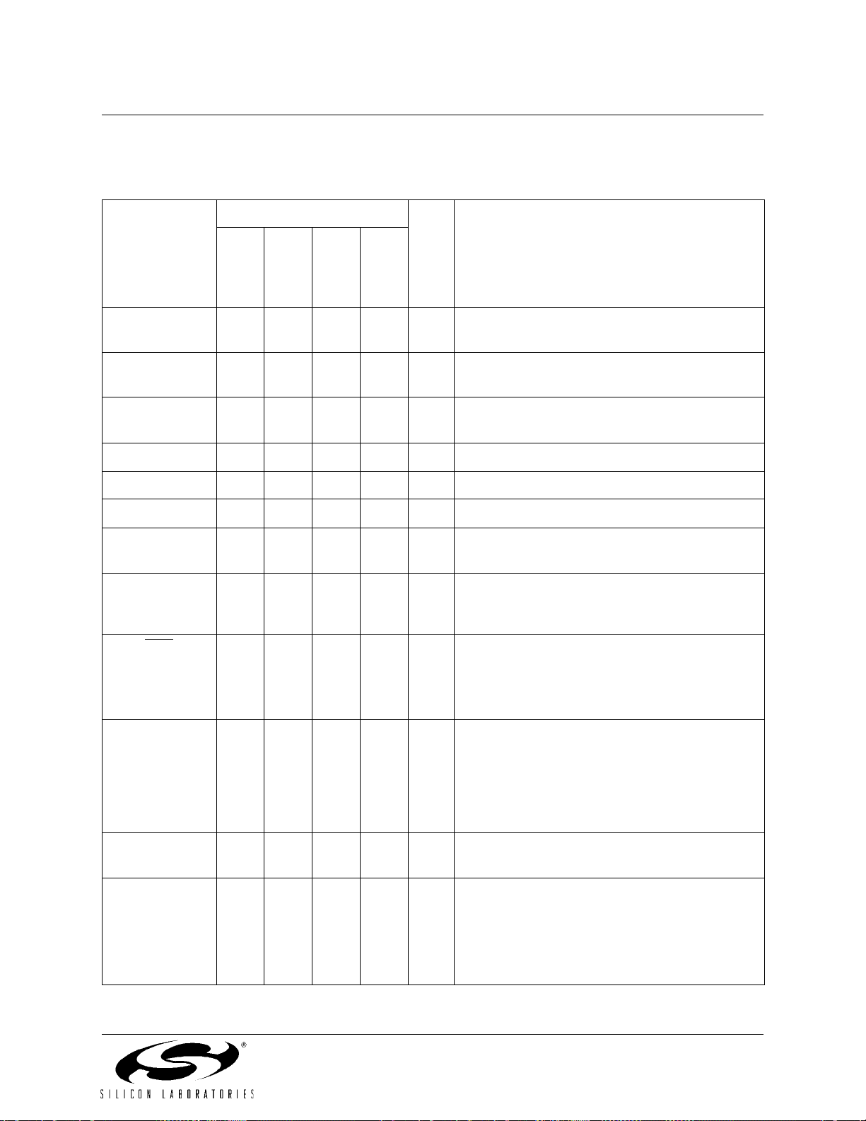
4. Pinout and Package Definitions
Table 4.1. Pin Definitions
Pin Numbers
C8051F120/1/2/3/4/5/6/7
C8051F130/1/2/3
Name
V
DD
DGND 38,
AV+ 11, 14 6 11, 14 6 Analog Supply Voltage. Must be tied to +2.7 to
AGND 10, 13 5 10, 13 5 Analog Ground. Must be tied to Ground.
TMS 1 58 1 5 8 D In JTAG Test Mode Select with internal pullup.
TCK 2 59 2 59 D In JTAG Test Clock with int ernal pullup.
TDI 3 60 3 60 D In JTAG Test Data Input with internal pullup. TDI is
TDO 4 61 4 61 D Out JTAG Test Data Output with internal pullup. Data
RST
‘F120
‘F122
‘F124
‘F126
64, 90
63, 89
‘F121
‘F123
‘F125
‘F127
37,
41, 57
40, 56
5 62 5 62 D I/O Device Reset. Open-drain output of internal VDD
24,
25,
‘F130
‘F132
37,
64, 90
38,
63, 89
‘F131
‘F133
24,
41, 57
25,
40, 56
Type Description
Digital Supply Voltage. Must be tied to +2.7 to
+3.6 V.
Digital Ground. Must be tied to Ground.
+3.6 V.
latched on the rising edge of TCK.
is shifted out on TDO on the falling edge of TCK.
TDO output is a tri-state driver.
monitor. Is driven low when V
MONEN is high. An external source can initiate
a system reset by driving this pin low.
DD
is < V
RST
and
XTAL1 26 17 26 17 A In Crystal Input. This pin is the return for the inter-
nal oscillator circuit for a crystal or ceramic resonator . For a precision internal clock, connect a
crystal or ceramic resonator from XTAL1 to
XTAL2. If overdriven by an external CMOS
clock, this becomes the system clock.
XTAL2 27 18 27 18 A Out Crystal Output. This pin is the excitation driver
for a crystal or ceramic resonator.
MONEN 28192819D InV
Rev. 1.4 41
Monitor Enable. When tied high, this pin
DD
enables the internal V
system reset when V
low, the internal V
This pin must be tied high or low.
monitor, which forces a
DD
is < V
DD
monitor is disabled.
DD
. When tied
RST

C8051F120/1/2/3/4/5/6/7
C8051F130/1/2/3
Table 4.1. Pin Definitions (Continued)
Pin Numbers
Name
VREF 1 2 7 12 7 A I/O Bandgap Voltage Reference Output
VREFA 8 A In ADC0 and ADC2 Voltage Reference Input.
VREF0 16 16 8 A In ADC0 Voltage Reference Input.
VREF2 17 17 A In ADC2 Voltage Reference Input.
VREFD 15 15 A In DAC Voltage Reference Input.
AIN0.0 18 9 18 9 A In ADC0 Input Channel 0 (See ADC0 S pe cification
AIN0.1 19 10 19 10 A In ADC0 Input Channel 1 (See ADC0 Specification
AIN0.2 20 11 20 11 A In ADC0 Input Channel 2 (See ADC0 Specification
AIN0.3 21 12 21 12 A In ADC0 Input Channel 3 (See ADC0 Specification
‘F120
‘F122
‘F124
‘F126
‘F121
‘F123
‘F125
‘F127
‘F130
‘F132
‘F131
‘F133
Type Description
(all devices).
DAC Voltage Reference Input
(C8051F121/3/5/7 only).
for complete description).
for complete description).
for complete description).
for complete description).
AIN0.4 22 13 22 13 A In ADC0 Input Channel 4 (See ADC0 Specification
for complete description).
AIN0.5 23 14 23 14 A In ADC0 Input Channel 5 (See ADC0 Specification
for complete description).
AIN0.6 24 15 24 15 A In ADC0 Input Channel 6 (See ADC0 Specification
for complete description).
AIN0.7 25 16 25 16 A In ADC0 Input Channel 7 (See ADC0 Specification
for complete description).
CP0+ 9 4 9 4 A In Comparator 0 Non-Inverting Input.
CP0- 8 3 8 3 A In Comparator 0 Inverting Input.
CP1+ 7 2 7 2 A In Comparator 1 Non-Inverting Input.
CP1– 6 1 6 1 A In Comparator 1 Inverting Input.
DAC0 100 64 A Out Digital to Analog Converter 0 Voltage Output.
(See DAC Specification for complete description).
42 Rev. 1.4
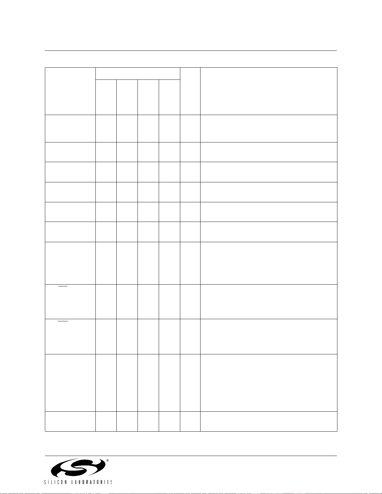
C8051F120/1/2/3/4/5/6/7
Table 4.1. Pin Definitions (Continued)
Pin Numbers
C8051F130/1/2/3
Name
DAC1 99 63 A Out Digital to Analog Converter 1 Voltage Output.
P0.0 62 55 62 55 D I/O Port 0.0. See Port Inp u t/O ut pu t se ctio n fo r c om-
P0.1 61 54 61 54 D I/O Port 0.1. See Port Inp u t/O ut pu t se ctio n fo r c om-
P0.2 60 53 60 53 D I/O Port 0.2. See Port Inp u t/O ut pu t se ctio n fo r c om-
P0.3 59 52 59 52 D I/O Port 0.3. See Port Inp u t/O ut pu t se ctio n fo r c om-
P0.4 58 51 58 51 D I/O Port 0.4. See Port Inp u t/O ut pu t se ctio n fo r c om-
ALE/P0.5 57 50 57 50 D I/O ALE Strobe for External Memory Address bus
‘F120
‘F122
‘F124
‘F126
‘F121
‘F123
‘F125
‘F127
‘F130
‘F132
‘F131
‘F133
Type Description
(See DAC Specification for complete description).
plete description.
plete description.
plete description.
plete description.
plete description.
(multiplexed mode)
Port 0.5
See Port Input/Output section for complete
description.
RD
/P0.6 56 49 56 49 D I/O /RD Strobe for External Memory Address bus
WR
/P0.7 55485548D I/O/WR Strobe for External Memory Address bus
AIN2.0/A8/P1.0 36 29 36 29 A In
D I/O
AIN2.1/A9/P1.1 35 28 35 28 A In
D I/O
Rev. 1.4 43
Port 0.6
See Port Input/Output section for complete
description.
Port 0.7
See Port Input/Output section for complete
description.
ADC2 Input Channel 0 (See ADC2 Specification
for complete description).
Bit 8 External Memory Address bus (Non-multiplexed mode)
Port 1.0
See Port Input/Output section for complete
description.
Port 1.1. See Port Input/Output section for complete description.

C8051F120/1/2/3/4/5/6/7
C8051F130/1/2/3
Table 4.1. Pin Definitions (Continued)
Pin Numbers
Name
AIN2.2/A10/P1.234273427A In
AIN2.3/A11/P1.3 33 26 33 26 A In
AIN2.4/A12/P1.432233223A In
AIN2.5/A13/P1.531223122A In
AIN2.6/A14/P1.630213021A In
AIN2.7/A15/P1.729202920A In
A8m/A0/P2.0 46 37 46 37 D I/O Bit 8 External Memory Address bus (Multiplexed
‘F120
‘F122
‘F124
‘F126
‘F121
‘F123
‘F125
‘F127
‘F130
‘F132
‘F131
‘F133
Type Description
Port 1.2. See Port Input/Output section for com-
D I/O
D I/O
D I/O
D I/O
D I/O
D I/O
plete description.
Port 1.3. See Port Input/Output section for com-
plete description.
Port 1.4. See Port Input/Output section for com-
plete description.
Port 1.5. See Port Input/Output section for com-
plete description.
Port 1.6. See Port Input/Output section for com-
plete description.
Port 1.7. See Port Input/Output section for com-
plete description.
mode)
Bit 0 External Memory Address bus (Non-multiplexed mode)
Port 2.0
See Port Input/Output section for complete
description.
A9m/A1/P2.145364536D I/OPort 2.1. See Port Input/Output section for com-
plete description.
A10m/A2/P2.2 44 35 44 35 D I/O Port 2.2. See Port Input/Outpu t se ctio n fo r com -
plete description.
A11m/A3/P2.3 43 34 43 34 D I/O Port 2.3. See Port Input/Output section for com-
plete description.
A12m/A4/P2.4 42 33 42 33 D I/O Port 2.4. See Port Input/Outpu t se ctio n fo r com -
plete description.
A13m/A5/P2.5 41 32 41 32 D I/O Port 2.5. See Port Input/Outpu t se ctio n fo r com -
plete description.
A14m/A6/P2.6 40 31 40 31 D I/O Port 2.6. See Port Input/Outpu t se ctio n fo r com -
plete description.
A15m/A7/P2.7 39 30 39 30 D I/O Port 2.7. See Port Input/Outpu t se ctio n fo r com -
plete description.
44 Rev. 1.4

C8051F120/1/2/3/4/5/6/7
Table 4.1. Pin Definitions (Continued)
Pin Numbers
C8051F130/1/2/3
Name
AD0/D0/P3.0 54 47 54 47 D I/O Bit 0 External Memory Address/Data bus (Multi-
AD1/D1/P3.153465346D I/OPort 3.1. See Port Input/Output section for com-
AD2/D2/P3.252455245D I/OPort 3.2. See Port Input/Output section for com-
AD3/D3/P3.351445144D I/OPort 3.3. See Port Input/Output section for com-
AD4/D4/P3.450435043D I/OPort 3.4. See Port Input/Output section for com-
AD5/D5/P3.549424942D I/OPort 3.5. See Port Input/Output section for com-
‘F120
‘F122
‘F124
‘F126
‘F121
‘F123
‘F125
‘F127
‘F130
‘F132
‘F131
‘F133
Type Description
plexed mode)
Bit 0 External Memory Data bus (Non-multiplexed mode)
Port 3.0
See Port Input/Output section for complete
description.
plete description.
plete description.
plete description.
plete description.
plete description.
AD6/D6/P3.648394839D I/OPort 3.6. See Port Input/Output section for com-
plete description.
AD7/D7/P3.747384738D I/OPort 3.7. See Port Input/Output section for com-
plete description.
P4.0 98 98 D I/O Port 4.0. See Port Input/Out pu t se ctio n fo r com-
plete description.
P4.1 97 97 D I/O Port 4.1. See Port Input/Out pu t se ctio n fo r com-
plete description.
P4.2 96 96 D I/O Port 4.2. See Port Input/Out pu t se ctio n fo r com-
plete description.
P4.3 95 95 D I/O Port 4.3. See Port Input/Out pu t se ctio n fo r com-
plete description.
P4.4 94 94 D I/O Port 4.4. See Port Input/Out pu t se ctio n fo r com-
plete description.
Rev. 1.4 45

C8051F120/1/2/3/4/5/6/7
C8051F130/1/2/3
Table 4.1. Pin Definitions (Continued)
Pin Numbers
Name
ALE/P4.5 93 93 D I/O ALE Strobe for External Memory Address bus
RD
/P4.6 92 92 D I/O /RD Strobe for External Memory Address bus
WR
/P4.7 91 91 D I/O /WR Strobe for External Memory Address bus
A8/P5.0 88 88 D I/O Bit 8 External Memory Address bus (Non-multi-
‘F120
‘F122
‘F124
‘F126
‘F121
‘F123
‘F125
‘F127
‘F130
‘F132
‘F131
‘F133
Type Description
(multiplexed mode)
Port 4.5
See Port Input/Output section for complete
description.
Port 4.6
See Port Input/Output section for complete
description.
Port 4.7
See Port Input/Output section for complete
description.
plexed mode)
Port 5.0
See Port Input/Output section for complete
description.
A9/P5.1 87 87 D I/O Port 5.1. See Port Input/Output section for com-
plete description.
A10/P5.2 86 86 D I/O Port 5.2. See Port Input/Output section for com-
plete description.
A11/P5.3 85 85 D I/O Port 5.3. See Port Input/Output section fo r com-
plete description.
A12/P5.4 84 84 D I/O Port 5.4. See Port Input/Output section for com-
plete description.
A13/P5.5 83 83 D I/O Port 5.5. See Port Input/Output section for com-
plete description.
A14/P5.6 82 82 D I/O Port 5.6. See Port Input/Output section for com-
plete description.
A15/P5.7 81 81 D I/O Port 5.7. See Port Input/Output section for com-
plete description.
46 Rev. 1.4

C8051F120/1/2/3/4/5/6/7
Table 4.1. Pin Definitions (Continued)
Pin Numbers
C8051F130/1/2/3
Name
A8m/A0/P6.0 80 80 D I/O Bit 8 External Memory Address bus (Multiplexed
A9m/A1/P6.1 79 79 D I/O Port 6.1. See Port Input/Output section for com-
A10m/A2/P6.2 78 78 D I/O Port 6.2. See Port Input/Output section for com-
A11m/A3/P6.3 77 77 D I/O Port 6.3. See Port Input/Output section for com-
A12m/A4/P6.4 76 76 D I/O Port 6.4. See Port Input/Output section for com-
A13m/A5/P6.5 75 75 D I/O Port 6.5. See Port Input/Output section for com-
‘F120
‘F122
‘F124
‘F126
‘F121
‘F123
‘F125
‘F127
‘F130
‘F132
‘F131
‘F133
Type Description
mode)
Bit 0 External Memory Address bus (Non-multiplexed mode)
Port 6.0
See Port Input/Output section for complete
description.
plete description.
plete description.
plete description.
plete description.
plete description.
A14m/A6/P6.6 74 74 D I/O Port 6.6. See Port Input/Output section for com-
plete description.
A15m/A7/P6.7 73 73 D I/O Port 6.7. See Port Input/Output section for com-
plete description.
AD0/D0/P7.0 72 72 D I/O Bit 0 External Memory Address/Data bus (Multi-
plexed mode)
Bit 0 External Memory Data bus (Non-multiplexed mode)
Port 7.0
See Port Input/Output section for complete
description.
AD1/D1/P7.1 71 71 D I/O Port 7.1. See Port Input/Output section for com-
plete description.
AD2/D2/P7.2 70 70 D I/O Port 7.2. See Port Input/Output section for com-
plete description.
AD3/D3/P7.3 69 69 D I/O Port 7.3. See Port Input/Output section for com-
plete description.
AD4/D4/P7.4 68 68 D I/O Port 7.4. See Port Input/Output section for com-
plete description.
Rev. 1.4 47
C8051F120/1/2/3/4/5/6/7
C8051F130/1/2/3
Table 4.1. Pin Definitions (Continued)
Pin Numbers
Name
AD5/D5/P7.5 67 67 D I/O Port 7.5. See Port Input/Output section for com-
AD6/D6/P7.6 66 66 D I/O Port 7.6. See Port Input/Output section for com-
AD7/D7/P7.7 65 65 D I/O Port 7.7. See Port Input/Output section for com-
NC 15,
‘F120
‘F122
‘F124
‘F126
‘F121
‘F123
‘F125
‘F127
‘F130
‘F132
17,
99,
100
‘F131
‘F133
63, 64 No Connection.
Type Description
plete description.
plete description.
plete description.
48 Rev. 1.4

C8051F120/1/2/3/4/5/6/7
C8051F130/1/2/3
DAC0
DAC1
P4.0
P4.1
P4.2
P4.3
P4.4
ALE/P4.5
/RD/P4.6
/WR/P4.7
VDD
DGND
A8/P5.0
A9/P5.1
A10/P5.2
A11/P5.3
A12/P5.4
A13/P5.5
A14/P5.6
A15/P5.7
A8m/A0/P6.0
A9m/A1/P6.1
A10m/A2/P6.2
A11m/A3/P6.3
A12m/A4/P6.4
TMS
TCK
TDI
TDO
/RST
CP1-
CP1+
CP0-
CP0+
AGND
AV+
VREF
AGND
AV+
VREFD
VREF0
VREF2
AIN0.0
AIN0.1
AIN0.2
AIN0.3
AIN0.4
AIN0.5
AIN0.6
AIN0.7
10
11
12
13
14
15
16
17
18
19
20
21
22
23
24
25
9998979695949392919089888786858483828180797877
100
1
2
3
4
5
6
7
8
9
C8051F120
C8051F122
C8051F124
C8051F126
76
75
A13m/A5/P6.5
74
A14m/A6/P6.6
73
A15m/A7/P6.7
72
AD0/D0/P7.0
71
AD1/D1/P7.1
70
AD2/D2/P7.2
69
AD3/D3/P7.3
68
AD4/D4/P7.4
67
AD5/D5/P7.5
66
AD6/D6/P7.6
65
AD7/D7/P7.7
64
VDD
63
DGND
62
P0.0
61
P0.1
60
P0.2
59
P0.3
58
P0.4
57
ALE/P0.5
56
/RD/P0.6
55
/WR/P0.7
54
AD0/D0/P3.0
53
AD1/D1/P3.1
52
AD2/D2/P3.2
51
AD3/D3/P3.3
262728293031323334353637383940
VDD
XTAL1
XTAL2
MONEN
AIN2.7/A15/P1.7
AIN2.6/A14/P1.6
AIN2.5/A13/P1.5
AIN2.4/A12/P1.4
AIN2.1/A9/P1.1
AIN2.3/A11/P1.3
AIN2.2/A10/P1.2
DGND
AIN2.0/A8/P1.0
41
424344454647484950
AD7/D7/P3.7
AD6/D6/P3.6
AD5/D5/P3.5
A9m/A1/P2.1
A15m/A7/P2.7
A14m/A6/P2.6
A13m/A5/P2.5
A12m/A4/P2.4
A11m/A3/P2.3
A8m/A0/P2.0
A10m/A2/P2.2
AD4/D4/P3.4
Figure 4.1. C8051F120/2/4/6 Pinout Diagram (TQFP-100)
Rev. 1.4 49
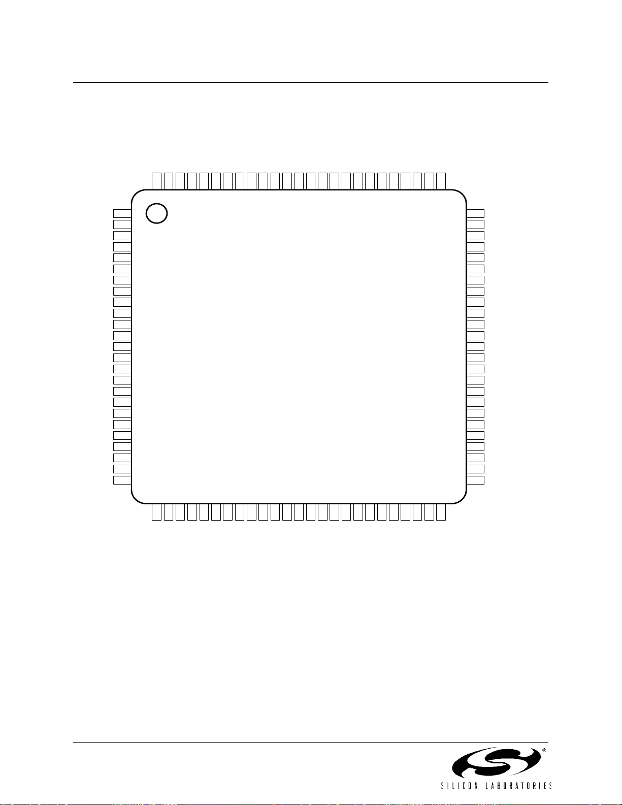
C8051F120/1/2/3/4/5/6/7
C8051F130/1/2/3
TMS
TCK
TDI
TDO
/RST
CP1-
CP1+
CP0-
CP0+
AGND
AV+
VREF
AGND
AV+
NC
VREF0
NC
AIN0.0
AIN0.1
AIN0.2
AIN0.3
AIN0.4
AIN0.5
AIN0.6
AIN0.7
10
11
12
13
14
15
16
17
18
19
20
21
22
23
24
25
NCNCP4.0
100
1
2
3
4
5
6
7
8
9
P4.1
P4.2
P4.3
P4.4
ALE/P4.5
/RD/P4.6
/WR/P4.7
VDD
DGND
A8/P5.0
A9/P5.1
A10/P5.2
A11/P5.3
A12/P5.4
A13/P5.5
A14/P5.6
A15/P5.7
A8m/A0/P6.0
A9m/A1/P6.1
A10m/A2/P6.2
A11m/A3/P6.3
9998979695949392919089888786858483828180797877
C8051F130
C8051F132
A12m/A4/P6.4
76
75
A13m/A5/P6.5
74
A14m/A6/P6.6
73
A15m/A7/P6.7
72
AD0/D0/P7.0
71
AD1/D1/P7.1
70
AD2/D2/P7.2
69
AD3/D3/P7.3
68
AD4/D4/P7.4
67
AD5/D5/P7.5
66
AD6/D6/P7.6
65
AD7/D7/P7.7
64
VDD
63
DGND
62
P0.0
61
P0.1
60
P0.2
59
P0.3
58
P0.4
57
ALE/P0.5
56
/RD/P0 .6
55
/WR/P 0 .7
54
AD0/D0/P3.0
53
AD1/D1/P3.1
52
AD2/D2/P3.2
51
AD3/D3/P3.3
262728293031323334353637383940
VDD
XTAL1
XTAL2
MONEN
AIN2.7/A15/P1.7
AIN2.6/A14/P1.6
AIN2.5/A13/P1.5
AIN2.4/A12/P1.4
AIN2.1/A9/P1.1
AIN2.3/A11/P1.3
AIN2.2/A10/P1.2
DGND
AIN2.0/A8/P1.0
A15m/A7/P2.7
Figure 4.2. C8051F130/2 Pinout Diagram (TQFP-100)
50 Rev. 1.4
41
424344454647484950
A9m/A1/P2.1
A14m/A6/P2.6
A13m/A5/P2.5
A12m/A4/P2.4
A11m/A3/P2.3
A8m/A0/P2.0
A10m/A2/P2.2
AD7/D7/P3.7
AD6/D6/P3.6
AD5/D5/P3.5
AD4/D4/P3.4

C8051F120/1/2/3/4/5/6/7
C8051F130/1/2/3
100
PIN 1
DESIGNATOR
D
D1
E1 E
1
A
A1
A2
b
D
D1
e
E
E1
L
MIN
(mm )
-
0.05
0.95
0.17
-
-
-
-
-
0.45
NOM
(mm)
-
-
1.00
0.22
16.00
14.00
0.50
16.00
14.00
0.60
MAX
(mm )
1.20
0.15
1.05
0.27
-
-
-
-
-
0.75
A2
e
A
L
b
A1
Figure 4.3. TQFP-100 Package Drawing
Rev. 1.4 51

C8051F120/1/2/3/4/5/6/7
C8051F130/1/2/3
DAC0
DAC1
/RST
TDO
TDI
TCK
TMS
64
63
62
61
60
59
58
VDD
57
DGND
56
P0.0
55
P0.1
54
P0.2
53
P0.3
52
P0.4
51
ALE/P0.5
50
/RD/P0.6
49
CP1-
CP1+
CP0-
CP0+
AGND
AV+
VREF
VREFA
AIN0.0
AIN0.1
AIN0.2
AIN0.3
AIN0.4
AIN0.5
AIN0.6
AIN0.7
1
2
3
4
5
6
7
8
9
10
11
12
13
14
15
16
17
18
19
C8051F121
C8051F123
C8051F125
C8051F127
20
21
22
23
24
25
26
27
28
29
30
31
32
48
/WR/P0.7
47
AD0/D0/P3.0
46
AD1/D1/P3.1
45
AD2/D2/P3.2
44
AD3/D3/P3.3
43
AD4/D4/P3.4
42
AD5/D5/P3.5
41
VDD
40
DGND
39
AD6/D6/P3.6
38
AD7/D7/P3.7
37
A8m/A0/P2.0
36
A9m/A1/P2.1
35
A10m/A2/P2.2
34
A11m/A3/P2.3
33
A12m/A4/P2.4
VDD
XTAL1
XTAL2
MONEN
AIN2.7/A15/P1.7
AIN2.6/A14/P1.6
AIN2.5/A13/P1.5
AIN2.4/A12/P1.4
DGND
Figure 4.4. C8051F121/3/5/7 Pinout Diagram (TQFP-64)
52 Rev. 1.4
AIN2.3/A11/P1.3
AIN2.2/A10/P1.2
A15m/A7/P2.7
A14m/A6/P2.6
AIN2.1/A9/P1.1
AIN2.0/A8/P1.0
A13m/A5/P2.5

NC
64
NC
63
/RST
62
TDO
61
TDI
60
TCK
59
TMS
58
C8051F120/1/2/3/4/5/6/7
C8051F130/1/2/3
VDD
DGND
P0.0
P0.1
P0.2
P0.3
P0.4
ALE/P0.5
/RD/P0.6
57
56
55
54
53
52
51
50
49
CP1-
CP1+
CP0-
CP0+
AGND
AV+
VREF
VREF0
AIN0.0
AIN0.1
AIN0.2
AIN0.3
AIN0.4
AIN0.5
AIN0.6
AIN0.7
10
11
12
13
14
15
16
1
2
3
4
5
6
7
8
9
17
18
19
C8051F131
C8051F133
20
21
22
23
24
25
26
27
28
29
30
31
32
48
/WR/P 0 .7
47
AD0/D0/P3.0
46
AD1/D1/P3.1
45
AD2/D2/P3.2
44
AD3/D3/P3.3
43
AD4/D4/P3.4
42
AD5/D5/P3.5
41
VDD
40
DGND
39
AD6/D6/P3.6
38
AD7/D7/P3.7
37
A8m/A0/P2.0
36
A9m/A1/P2.1
35
A10m/A2/P2.2
34
A11m/A3/P2.3
33
A12m/A4/P2.4
VDD
XTAL1
XTAL2
MONEN
AIN2.7/A15/P1.7
AIN2.6/A14/P1.6
AIN2.5/A13/P1.5
AIN2.4/A12/P1.4
DGND
A15m/A7/P2.7
A14m/A6/P2.6
AIN2.1/A9/P1.1
AIN2.3/A11/P1.3
AIN2.2/A10/P1.2
AIN2.0/A8/P1.0
A13m/A5/P2.5
Figure 4.5. C8051F131/3 Pinout Diagram (TQFP-64)
Rev. 1.4 53

C8051F120/1/2/3/4/5/6/7
C8051F130/1/2/3
D
D1
E1
MIN
(mm)
A
A1
0.05
A2
0.95
E
b
0.17
D
-
-
NOM
(mm )
-
-
1.00
0.22
12.00
MAX
(mm )
1.20
0.15
1.05
0.27
-
64
1
e
b
A1
Figure 4.6. TQFP-64 Package Drawing
D1
e
E
E1
L
-
-
-
-
0.45
10.00
0.50
12.00
10.00
0.60
-
-
-
-
0.75
54 Rev. 1.4
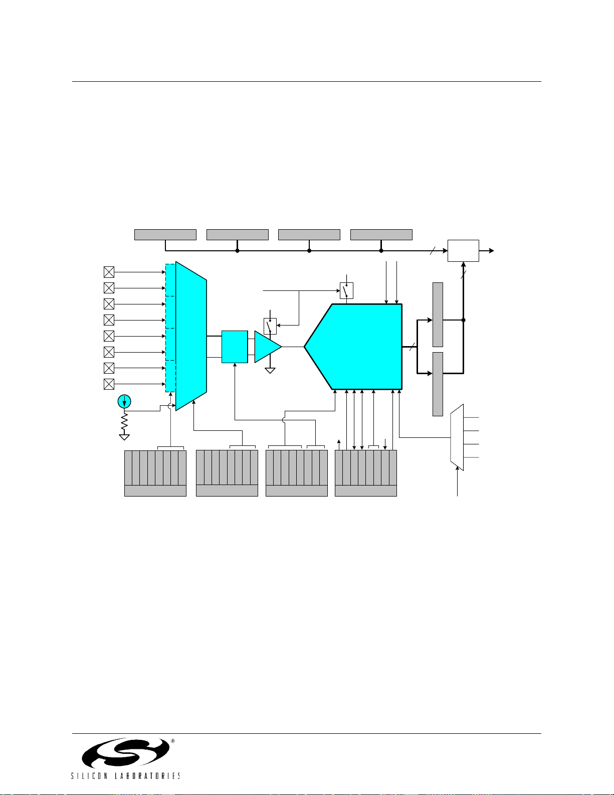
C8051F120/1/2/3/4/5/6/7
C8051F130/1/2/3
5. ADC0 (12-Bit ADC, C8051F120/1/4/5 Only)
The ADC0 subsystem for the C8051F120/1/4/5 consists of a 9-channel, configurable analog multiplexer
(AMUX0), a programmable gain amplifier (PGA0), and a 100 ksps, 12-bit successive-approximation-register ADC with integrated track-and-hold and Programmable Window Detector (see block diagram in
Figure 5.1). The AMUX0, PGA0, Data Conversion Modes, and Window Detector are all configurable under
software control via the Special Function Registers shown in Figure 5.1. The voltage reference used by
ADC0 is selected as described in
(ADC0, track-and-hold and PGA0) is enabled only when the AD0EN bit in the ADC0 Control register
(ADC0CN) is set to logic 1. The ADC0 subsystem is in low power shutdown when this bit is logic 0.
TEMP
+
+
+
+
-
9-to-1
AMUX
(SE or
DIFF)
AIN0.0
AIN0.1
AIN0.2
AIN0.3
AIN0.4
AIN0.5
AIN0.6
AIN0.7
SENSOR
AGND
Section “9. Voltage Reference” on page 113. The ADC0 subsystem
ADC0LTLADC0LTHADC0GTLADC0GTH
24
AD0EN
AV+
AV+
REF
SYSCLK
Comb.
Logic
12
AD0WINT
12-Bit
X
+
SAR
-
AGND
ADC
AD0CM
12
Start Conversion
ADC0L ADC0H
00
01
10
11
AD0BUSY (W)
Timer 3 Overflow
CNVSTR0
Timer 2 Overflow
AIN01IC
AIN23IC
AIN45IC
AIN67IC
AMX0CF
AMX0SL
AMX0AD0
AMX0AD1
AMX0AD2
AMX0AD3
AD0SC3
AD0SC4
ADC0CF
AD0SC1
AD0SC2
AMP0GN2
AD0SC0
AMP0GN0
AMP0GN1
AD0INT
AD0TM
AD0EN
ADC0CN
AD0WINT
AD0CM0
AD0CM1
AD0BUSY
AD0LJST
AD0CM
Figure 5.1. 12-Bit ADC0 Functional Block Diagram
5.1. Analog Multiplexer and PGA
Eight of the AMUX channels are available for external measurements while the ninth channel is internally
connected to an on-chip temperature sensor (temperature transfer function is shown in Figure 5.2). AMUX
input pairs can be programmed to operate in either differential or single-ended mode. This allows the user
to select the best measurement technique for each input channel, and even accommodates mode
changes "on-the-fly". The AMUX defaults to all single-ended inputs upon reset. There are two registers
associated with the AMUX: the Channel Selection register AMX0SL (SFR Definition 5.2), and the Configuration register AMX0CF (SFR Definition 5.1). The table in SFR Definition 5.2 shows AMUX functionality by
channel, for each possible configuration. The PGA amplifies the AMUX output signal by an amount determined by the states of the AMP0GN2-0 bits in the ADC0 Configuration register, ADC0CF (SFR Definition
5.3). The PGA can be software-programmed for gains of 0.5, 2, 4, 8 or 16. Gain defaults to unity on reset.
Rev. 1.4 55

C8051F120/1/2/3/4/5/6/7
C8051F130/1/2/3
The Temperature Sensor transfer function is shown in Figure 5.2. The output voltage (V
input when the Temperature Sensor is selected by bits AMX0AD3-0 in register AMX0SL; this voltage will
be amplified by the PGA according to the user-programm ed PGA settings. Typical values for the Slope and
Offset parameters can be found in Table 5.1.
Slope (V / deg C)
Offset (V at 0 Celsius)
) is the PGA
TEMP
Voltage
V
= (Slope x TempC) + Offset
TEMP
Temp
= (V
C
0-50 50 100
- Offset) / Slope
TEMP
Temperature (Celsius)
Figure 5.2. Typical Temperature Sensor Transfer Function
56 Rev. 1.4

C8051F120/1/2/3/4/5/6/7
C8051F130/1/2/3
5.2. ADC Modes of Operation
ADC0 has a maximum conversion speed of 100 ksps. The ADC0 conversion clock is derived from the system clock divided by the value held in the ADCSC bits of register ADC0CF.
5.2.1. Starting a Conversion
A conversion can be initiated in one of four ways, depending on the programmed states of the ADC0 Start
of Conversion Mode bits (AD0CM1, AD0CM0) in ADC0CN. Conversions may be initiated by:
1. Writing a ‘1’ to the AD0BUSY bit of ADC0CN;
2. A Timer 3 overflow (i.e. timed continuous conversions);
3. A rising edge detected on the external ADC convert start signal, CNVSTR0;
4. A Timer 2 overflow (i.e. timed continuous conversions).
The AD0BUSY bit is set to logic 1 during conversion and restored to logic 0 when conversion is complete.
The falling edge of AD0BUSY triggers an interrupt (when enabled) and sets the AD0INT interrupt flag
(ADC0CN.5). Converted data is available in the ADC0 data word MSB and LSB registers, ADC0H, ADC0 L.
Converted data can be either left or right justified in the ADC0H:ADC0L register pair (see example in
Figure 5.5) depending on the programmed state of the AD0LJST bit in the ADC0CN register.
When initiating conversions by writ ing a ‘1’ to AD0BUSY, the AD0INT bit should be polled to determine
when a conversion has completed (ADC0 interrupts may also be used). The recommended polling procedure is shown below.
Step 1. Write a ‘0’ to AD0INT;
Step 2. Write a ‘1’ to AD0BUSY;
Step 3. Poll AD0INT for ‘1’;
Step 4. Process ADC0 data.
When CNVSTR0 is used as a conversion start source, it must be enabled in th e crossbar, and the corresponding pin must be set to open-drain, high-impedance mode (see
page 235
for more details on Port I/O configuration).
Section “18. Port Input/Output” on
Rev. 1.4 57
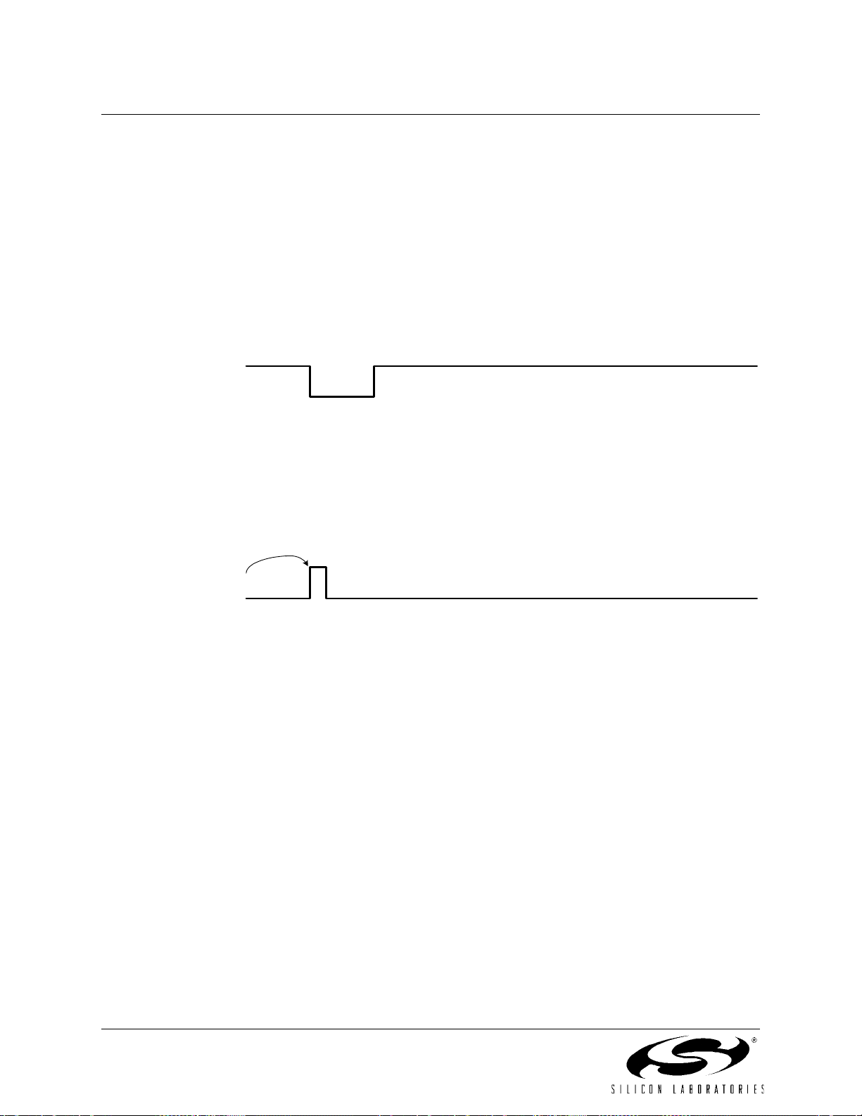
C8051F120/1/2/3/4/5/6/7
C8051F130/1/2/3
5.2.2. Tracking Modes
The AD0TM bit in register ADC0CN controls the ADC0 track-and-hold mode. In its default state, the ADC0
input is continuously tracked when a conversion is not in progress. When the AD0TM bit is logic 1, ADC0
operates in low-power track-and-hold mode. In this mode, each conversion is preceded by a tracking
period of 3 SAR clocks (after the start-of-conversion signal). When the CNVSTR0 signal is used to initiate
conversions in low-power tracking mode, ADC0 tra cks only when CNVSTR0 is low; conversion begins on
the rising edge of CNVSTR0 (see Figure 5.3). Tracking can also be disabled (shutdown) when the entire
chip is in low power standby or sleep modes. Low-power track-and-hold mode is also useful when AMUX
or PGA settings are frequently changed, to ensure that settling time requirements are met (see
“5.2.3. Settling Time Requirements” on page 59
).
A. ADC Timing for External Trigger Source
CNVSTR0
(AD0CM[1:0]=10)
12345678910111213141516
SAR Clocks
ADC0TM=1
Section
ADC0TM=0
Timer 2, Timer 3 Overflow;
Write '1' to AD0BUSY
(AD0CM[1:0]=00, 01, 11)
ADC0TM=1
ADC0TM=0
Figure 5.3. ADC0 Track and Conversion Example Timing
B. ADC Timing for Internal Trigger Sources
58 Rev. 1.4

C8051F120/1/2/3/4/5/6/7
C8051F130/1/2/3
5.2.3. Settling Time Requirements
A minimum tracking time is required before an accurate conversion can be performed. This tracking time is
determined by the ADC0 MUX resistance, the ADC0 sampling capacitance, any external source re sistance, and the accuracy required for the conversion. Figure 5.4 shows the equivalent ADC0 input circuits
for both Differential and Single-ended modes. Notice that the equivalent time constant for both input circuits is the same. The required settling time for a given settling accuracy (
Equation 5.1. When measuring the Temperature Sensor output,
R
TOTAL
minimum settling time of 1.5 µs is required after any MUX or PGA selection. Note that in low-power tracking mode, three SAR clocks are used for tracking at the start of ever y conversion. For most application s,
these three SAR clocks will meet the tracking requirements.
n
2
⎛⎞
------ -
t
×ln=
⎝⎠
SA
R
TOTALCSAMPLE
Equation 5.1. ADC0 Settling Time Requirements
Where:
SA is the settling accuracy, given as a fraction of an LSB (for example, 0.25 to settle within 1/4 LSB)
t is the required settling time in seconds
R
n is the ADC resolution in bits (12).
is the sum of the ADC0 MUX resistance and any external source resistance.
TOTAL
SA) may be approximated by
reduces to R
. An absolute
MUX
AIN0.x
AIN0.y
Differential Mode
MUX Select
R
= 5k
MUX
RC
= R
Input
MUX Select
* C
MUX
SAMPLE
R
= 5k
MUX
Figure 5.4. ADC0 Equivalent Input Circuits
C
C
SAMPLE
SAMPLE
= 10pF
= 10pF
Single-Ended Mode
MUX Select
AIN0.x
RC
Input
= R
MUX
R
* C
MUX
SAMPLE
= 5k
C
SAMPLE
= 10pF
Rev. 1.4 59

C8051F120/1/2/3/4/5/6/7
C8051F130/1/2/3
SFR Definition 5.1. AMX0CF: AMUX0 Configuration
SFR Page:
SFR Address:
R/W R/W R/W R/W R/W R/W R/W R/W Reset Value
Bit7 Bit6 Bit5 Bit4 Bit3 Bit2 Bit1 Bit0
Bits7–4: UNUSED. Read = 0000 b; Write = don’t care.
Bit3: AIN67IC: AIN0.6, AIN0.7 Input Pair Configuration Bit.
Bit2: AIN45IC: AIN0.4, AIN0.5 Input Pair Configuration Bit.
Bit1: AIN23IC: AIN0.2, AIN0.3 Input Pair Configuration Bit.
Bit0: AIN01IC: AIN0.0, AIN0.1 Input Pair Configuration Bit.
Note: The ADC0 Data Word is in 2’s complement format for channels configured as differential.
0
0xBA
- - - - AIN67IC AIN45IC AIN23IC AIN01IC 00000000
0: AIN0.6 and AIN0.7 are independent single-ended input s.
1: AIN0.6, AIN0.7 are (respectively) +, – differential input pair.
0: AIN0.4 and AIN0.5 are independent single-ended input s.
1: AIN0.4, AIN0.5 are (respectively) +, – differential input pair.
0: AIN0.2 and AIN0.3 are independent single-ended input s.
1: AIN0.2, AIN0.3 are (respectively) +, – differential input pair.
0: AIN0.0 and AIN0.1 are independent single-ended input s.
1: AIN0.0, AIN0.1 are (respectively) +, – differential input pair.
60 Rev. 1.4

C8051F120/1/2/3/4/5/6/7
C8051F130/1/2/3
SFR Definition 5.2. AMX0SL: AMUX0 Channel Select
SFR Page:
SFR Address:
R/W R/W R/W R/W R/W R/W R/W R/W Reset Value
0
0xBB
- - - - AMX0AD3 AMX0AD2 AMX0AD1 AMX0AD0 00000000
Bit7 Bit6 Bit5 Bit4 Bit3 Bit2 Bit1 Bit0
Bits7–4: UNUSED. Read = 0000 b; Write = don’t care.
Bits3–0: AMX0AD3–0: AMX0 Address Bits.
0000-1111b: ADC Inputs selected per chart below.
AMX0AD3–0
0000 0001 0010 0011 0100 0101 0110 0111 1xxx
AIN0.0 AIN0.1 AIN0.2 AIN0.3 AIN0.4 AIN0.5 AIN0.6 AIN0.7
+(AIN0.0)
–(AIN0.1)
AIN0.0 AIN0.1
+(AIN0.0)
–(AIN0.1)
AIN0.0 AIN0.1 AIN0.2 AIN0.3
+(AIN0.0)
–(AIN0.1)
AIN0.0 AIN0.1
+(AIN0.0)
–(AIN0.1)
AIN0.0 AIN0.1 AIN0.2 AIN0.3 AIN0.4 AIN0.5
+(AIN0.0)
–(AIN0.1)
AIN0.0 AIN0.1
+(AIN0.0)
–(AIN0.1)
AIN0.0 AIN0.1 AIN0.2 AIN0.3
+(AIN0.0)
–(AIN0.1)
AIN0.0 AIN0.1
+(AIN0.0)
–(AIN0.1)
AIN0.2 AIN0.3 AIN0.4 AIN0.5 AIN0.6 AIN0.7
+(AIN0.2)
–(AIN0.3)
+(AIN0.2)
–(AIN0.3)
AIN0.2 AIN0.3
+(AIN0.2)
–(AIN0.3)
+(AIN0.2)
–(AIN0.3)
AIN0.2 AIN0.3 AIN0.4 AIN0.5
+(AIN0.2)
–(AIN0.3)
+(AIN0.2)
–(AIN0.3)
AIN0.2 AIN0.3
+(AIN0.2)
–(AIN0.3)
+(AIN0.2)
–(AIN0.3)
AIN0.4 AIN0.5 AIN0.6 AIN0.7
AIN0.4 AIN0.5 AIN0.6 AIN0.7
+(AIN0.4)
–(AIN0.5)
+(AIN0.4)
–(AIN0.5)
+(AIN0.4)
–(AIN0.5)
+(AIN0.4)
–(AIN0.5)
AIN0.4 AIN0.5
AIN0.4 AIN0.5
+(AIN0.4)
–(AIN0.5)
+(AIN0.4)
–(AIN0.5)
+(AIN0.4)
–(AIN0.5)
+(AIN0.4)
–(AIN0.5)
AIN0.6 AIN0.7
AIN0.6 AIN0.7
AIN0.6 AIN0.7
AIN0.6 AIN0.7
+(AIN0.6)
–(AIN0.7)
+(AIN0.6)
–(AIN0.7)
+(AIN0.6)
–(AIN0.7)
+(AIN0.6)
–(AIN0.7)
+(AIN0.6)
–(AIN0.7)
+(AIN0.6)
–(AIN0.7)
+(AIN0.6)
–(AIN0.7)
+(AIN0.6)
–(AIN0.7)
AMX0CF Bits 3–0
0000
0001
0010
0011
0100
0101
0110
0111
1000
1001
1010
1011
1100
1101
1110
1111
TEMP
SENSOR
TEMP
SENSOR
TEMP
SENSOR
TEMP
SENSOR
TEMP
SENSOR
TEMP
SENSOR
TEMP
SENSOR
TEMP
SENSOR
TEMP
SENSOR
TEMP
SENSOR
TEMP
SENSOR
TEMP
SENSOR
TEMP
SENSOR
TEMP
SENSOR
TEMP
SENSOR
TEMP
SENSOR
Rev. 1.4 61

C8051F120/1/2/3/4/5/6/7
C8051F130/1/2/3
SFR Definition 5.3. ADC0CF: ADC0 Configuration
SFR Page:
SFR Address:
R/W R/W R/W R/W R/W R/W R/W R/W Reset Value
AD0SC4 AD0SC3 AD0SC2 AD0SC1 AD0SC0 AMP0GN2 AMP0GN1 AMP0GN0 11111000
Bit7 Bit6 Bit5 Bit4 Bit3 Bit2 Bit1 Bit0
Bits7–3: AD0SC4–0: ADC0 SAR Conversion Clock Period Bits.
Bits2–0: AMP0GN2–0: ADC0 Internal Amplifier Gain (PGA).
0
0xBC
The SAR Conversion clock is derived from system clock by the following equation, where
AD0SC refers to the 5-bit value held in AD0SC4-0, a nd CLK
SAR clock (Note: the ADC0 SAR Conversion Clock should be less than or equal to
2.5 MHz).
SYSCLK
AD0SC
When the AD0SC bits are equal to 00000b, the SAR Conversion clock is equal to SYSCLK
to facilitate faster ADC conversions at slower SYSCLK speeds.
000: Gain = 1
001: Gain = 2
010: Gain = 4
01 1: Gain = 8
10x: Gain = 16
11x: Gain = 0.5
-------------------------------2 C× LK
SAR0
1–= AD0SC 00000b>()
refers to the desired ADC0
SAR0
62 Rev. 1.4

C8051F120/1/2/3/4/5/6/7
C8051F130/1/2/3
SFR Definition 5.4. ADC0CN: ADC0 Control
SFR Page:
SFR Address:
R/W R/W R/W R/W R/W R/W R/W R/W Reset Value
AD0EN AD0TM AD0INT AD0BUSY AD0CM1 AD0CM0 AD0WINT AD0LJST 00000000
Bit7 Bit6 Bit5 Bit4 Bit3 Bit2 Bit1 Bit0
Bit7: AD0EN: ADC0 Enable Bit.
Bit6: AD0TM: ADC Track Mode Bit.
Bit5: AD0INT: ADC0 Conversion Complete Interrupt Flag.
Bit4: AD0BUSY: ADC0 Busy Bit.
Bits3–2: AD0CM1–0: ADC0 Start of Conversion Mode Select.
Bit1: AD0WINT: ADC0 Window Compare Interrupt Fla g.
Bit0: AD0LJST: ADC0 Left Justify Select.
0
0xE8 (bit addressa ble )
0: ADC0 Disabled. ADC0 is in low-power shutdown.
1: ADC0 Enabled. ADC0 is active and ready for data conversions.
0: When the ADC is enabled, tracking is continuous unless a conversion is in process.
1: Tracking Defined by ADCM1-0 bit s.
This flag must be cleared by software.
0: ADC0 has not completed a data conversion since the last time this flag was cleared .
1: ADC0 has completed a data conversion.
Read:
0: ADC0 Conversion is complete or a conversion is not currently in progress. AD0INT is set
to logic 1 on the falling edge of AD0BUSY.
1: ADC0 Conversion is in progress.
Write:
0: No Effect.
1: Initiates ADC0 Conversion if AD0CM1-0 = 00b.
If AD0TM = 0:
00: ADC0 conversion initiated on every write of ‘1’ to AD0BUSY.
01: ADC0 conversion initiated on overflow of Timer 3.
10: ADC0 conversion initiated on rising edge of external CNVSTR0.
11: ADC0 conversion initiated on overflow of Timer 2.
If AD0TM = 1:
00: Tracking starts with the write of ‘1’ to AD0BUSY and lasts for 3 SAR clocks, followed by
conversion.
01: Tracking started by the overflow of Timer 3 and lasts for 3 SAR clocks, followed by conversion.
10: ADC0 tracks only when CNVSTR0 input is logic low; conversion starts on rising
CNVSTR0 edge.
11: Tracking star ted by the overflow of Timer 2 and lasts for 3 SAR clocks, followed by conversion.
This bit must be cleared by software.
0: ADC0 Window Comparison Data match has not occurred since this flag was last cleared.
1: ADC0 Window Comparison Data match has occurred.
0: Data in ADC0H:ADC0L registers are right-justified.
1: Data in ADC0H:ADC0L registers are left-justified.
Rev. 1.4 63
C8051F120/1/2/3/4/5/6/7
C8051F130/1/2/3
SFR Definition 5.5. ADC0H: ADC0 Data Word MSB
SFR Page:
SFR Address:
R/W R/W R/W R/W R/W R/W R/W R/W Reset Value
Bit7 Bit6 Bit5 Bit4 Bit3 Bit2 Bit1 Bit0
Bits7–0: ADC0 Data Word High-Order Bits.
0
0xBF
00000000
For AD0LJST = 0: Bits 7–4 are the sign extension of Bit3 . Bits 3–0 are the upp er 4 bits of the
12-bit ADC0 Data Word.
For AD0LJST = 1: Bits 7–0 are the most-significant bits of the 12-bit ADC0 Data Word.
SFR Definition 5.6. ADC0L: ADC0 Data Word LSB
SFR Page:
SFR Address:
R/W R/W R/W R/W R/W R/W R/W R/W Reset Value
Bit7 Bit6 Bit5 Bit4 Bit3 Bit2 Bit1 Bit0
0
0xBE
00000000
Bits7–0: ADC0 Data Word Low-Order Bits.
For AD0LJST = 0: Bits 7–0 are the lower 8 bits of the 12-bit ADC0 Data Word.
For AD0LJST = 1: Bits 7–4 are the lower 4 bits of the 12-bit ADC0 Data Word. Bits 3–0 will
always read ‘0’.
64 Rev. 1.4

C8051F120/1/2/3/4/5/6/7
C8051F130/1/2/3
12-bit ADC0 Data Word appear s in the ADC0 Data Word Registers as follows:
ADC0H[3:0]:ADC0L[7:0], if AD0LJST = 0
(ADC0H[7:4] will be sign-extension of ADC0H.3 for a differential reading, otherwise
=
0000b).
ADC0H[7:0]:ADC0L[7:4], if AD0LJST = 1
(ADC0L[3:0] = 0000b).
Example: ADC0 Data Word Conversion Map , AIN0 .0 Input in Single-Ended Mode
(AMX0CF = 0x00, AMX0SL = 0x00)
AIN0.0–AGND
(Volts)
VREF x (4095/4096) 0x0FFF 0xFFF0
VREF / 2 0x0800 0x8000
VREF x (2047/4096) 0x07FF 0x7FF0
0 0x0000 0x0000
Example: ADC0 Data Word Conversion Map, AIN0.0 -AIN0.1 Differential Input Pair
(AMX0CF = 0x01, AMX0SL = 0x00)
AIN0.0–AIN0.1
(Volts)
VREF x (2047/2048) 0x07FF 0x7FF0
VREF / 2 0x0400 0x4000
VREF x (1/2048) 0x0001 0x0010
0 0x0000 0x0000
–VREF x (1/2048) 0xFFFF (–1d) 0xFFF0
–VREF / 2 0xFC00 (–1024d) 0xC000
–VREF 0xF800 (–2048d) 0x8000
For AD0LJST = 0:
Code Vin
× 2n×=
ADC0H:ADC0L
(AD0LJST = 0)
ADC0H:ADC0L
(AD0LJST = 0)
Gain
---------------
VREF
ADC0H:ADC0L
(AD0LJST = 1)
ADC0H:ADC0L
(AD0LJST = 1)
; ‘n’ = 12 for Single-Ended; ‘n’=11 for Differential.
Figure 5.5. ADC0 Data Word Example
Rev. 1.4 65
C8051F120/1/2/3/4/5/6/7
C8051F130/1/2/3
5.3. ADC0 Programmable Window Detector
The ADC0 Programmable Window Detector continuously compares th e ADC0 output to user-pr ogra mme d
limits, and notifies the system when an out-of-boun d condi tion is detected. This is especially effective in an
interrupt-driven system, saving code space and CPU bandwidth while delivering faster system response
times. The window detector interrupt flag (AD0WINT in ADC0CN) can also be used in polled mode. The
high and low bytes of the reference words are loaded into the ADC0 Greater-Than and ADC0 Less-Than
registers (ADC0GTH, ADC0GTL, ADC0LTH, and ADC0LTL). Reference comparisons are shown starting
on page 68. Notice that the window detector flag can be asserted when th e measur ed data is inside or outside the user-programmed limits, depending on the programming of the ADC0GTx and ADC0LTx registers.
SFR Definition 5.7. ADC0GTH: ADC0 Greater-Than Data High Byte
SFR Page:
SFR Address:
R/W R/W R/W R/W R/W R/W R/W R/W Reset Value
Bit7 Bit6 Bit5 Bit4 Bit3 Bit2 Bit1 Bit0
Bits7–0: High byte of ADC0 Greater-Than Data Word.
0
0xC5
SFR Definition 5.8. ADC0GTL: ADC0 Greater-Than Data Low Byte
SFR Page:
SFR Address:
R/W R/W R/W R/W R/W R/W R/W R/W Reset Value
Bit7 Bit6 Bit5 Bit4 Bit3 Bit2 Bit1 Bit0
Bits7–0: Low byte of ADC0 Greater-Tha n Da ta Word.
0
0xC4
11111111
11111111
66 Rev. 1.4
C8051F120/1/2/3/4/5/6/7
C8051F130/1/2/3
SFR Definition 5.9. ADC0LTH: ADC0 Less-Than Data High Byte
SFR Page:
SFR Address:
R/W R/W R/W R/W R/W R/W R/W R/W Reset Value
Bit7 Bit6 Bit5 Bit4 Bit3 Bit2 Bit1 Bit0
Bits7–0: High byte of ADC0 Less-Than Data Word.
0
0xC7
SFR Definition 5.10. ADC0LTL: ADC0 Less-Than Data Low Byte
SFR Page:
SFR Address:
R/W R/W R/W R/W R/W R/W R/W R/W Reset Value
Bit7 Bit6 Bit5 Bit4 Bit3 Bit2 Bit1 Bit0
Bits7–0: Low byte of ADC0 Less-Than Data Word.
0
0xC6
00000000
00000000
Rev. 1.4 67

C8051F120/1/2/3/4/5/6/7
C8051F130/1/2/3
Input Voltage
(AD0.0 - AGND)
REF x (4095/4096)
REF x (512/4096)
REF x (256/4096)
0
ADC Data
Word
0x0FFF
0x0201
0x0200
0x01FF
0x0101
0x0100
0x00FF
0x0000
AD0WINT
not affected
ADC0LTH:ADC0LTL
AD0WINT=1
ADC0GTH:ADC0GTL
AD0WINT
not affected
Given:
AMX0SL = 0x00, AMX0CF = 0x00
AD0LJST = ‘0’,
ADC0LTH:ADC0LTL = 0x0200,
ADC0GTH:ADC0GTL = 0x0100.
An ADC0 End of Conversion will cause an
ADC0 Window Compare Interrupt (AD0WINT
= ‘1’) if the resulting ADC0 Data Word is
< 0x0200 and > 0x0100.
Input Voltage
(AD0.0 - AGND)
REF x (4095/4096)
REF x (512/4096)
REF x (256/4096)
0
ADC Data
Word
0x0FFF
0x0201
0x0200
0x01FF
0x0101
0x0100
0x00FF
0x0000
AD0WINT=1
ADC0GTH:ADC0GTL
AD0WINT
not affected
ADC0LTH:ADC0LTL
AD0WINT=1
Given:
AMX0SL = 0x00, AMX0CF = 0x00,
AD0LJST = ‘0’,
ADC0LTH:ADC0LTL = 0x0100,
ADC0G TH:ADC0GTL = 0x0200.
An ADC0 End of Conversion will cause an
ADC0 Window Compare Interrupt (AD0WINT
= ‘1’) if the resulting ADC0 Data Word is
> 0x0200 or < 0x0100.
Figure 5.6. 12-Bit ADC0 Window Interrupt Example: Right Justified Single-Ended
Data
68 Rev. 1.4

C8051F120/1/2/3/4/5/6/7
C8051F130/1/2/3
Input Voltage
(AD0.0 - AD0 .1)
REF x (2047/2048)
REF x (256/2048)
REF x (-1/2048)
-REF
ADC Data
Word
0x07FF
0x0101
0x0100
0x00FF
0x0000
0xFFFF
0xFFFE
0xF800
AD0WINT
not affected
ADC0LTH:ADC0LTL
AD0WINT=1
ADC0GTH:ADC0GTL
AD0WINT
not affected
Given:
AMX0SL = 0x00, AMX0CF = 0x01,
AD0LJST = ‘0’,
ADC0LTH:ADC0LTL = 0x0100,
ADC0GTH:ADC0GTL = 0xFFFF.
An ADC0 End of Conversion will cause an
ADC0 Window Compare Interrupt (AD0WINT
= ‘1’) if the resulting ADC0 Data Word is
< 0x0100 and > 0xFFFF. (In 2s-complement
math, 0xFFFF = -1.)
Input Voltage
(AD0.0 - AD0 .1)
REF x (2047/2048)
REF x (256/2048)
REF x (-1/2048)
-REF
ADC Data
Word
0x07FF
0x0101
0x0100
0x00FF
0x0000
0xFFFF
0xFFFE
0xF800
AD0WINT=1
ADC0GTH:ADC0GTL
AD0WINT
not affected
ADC0LTH:ADC0LTL
AD0WINT=1
Given:
AMX0SL = 0x00, AMX0CF = 0x01,
AD0LJST = ‘0’,
ADC0LTH:ADC0LTL = 0xFFFF,
ADC0G TH:ADC0GTL = 0x0100.
An ADC0 End of Conversion will cause an
ADC0 Window Compare Interrupt (AD0WINT
= ‘1’) if the resulting ADC0 Data Word is
< 0xFFFF or > 0x0100. (In 2s-complement
math, 0xFFFF = -1.)
Figure 5.7. 12-Bit ADC0 Window Interrupt Example: Right Justified Differential
Data
Rev. 1.4 69
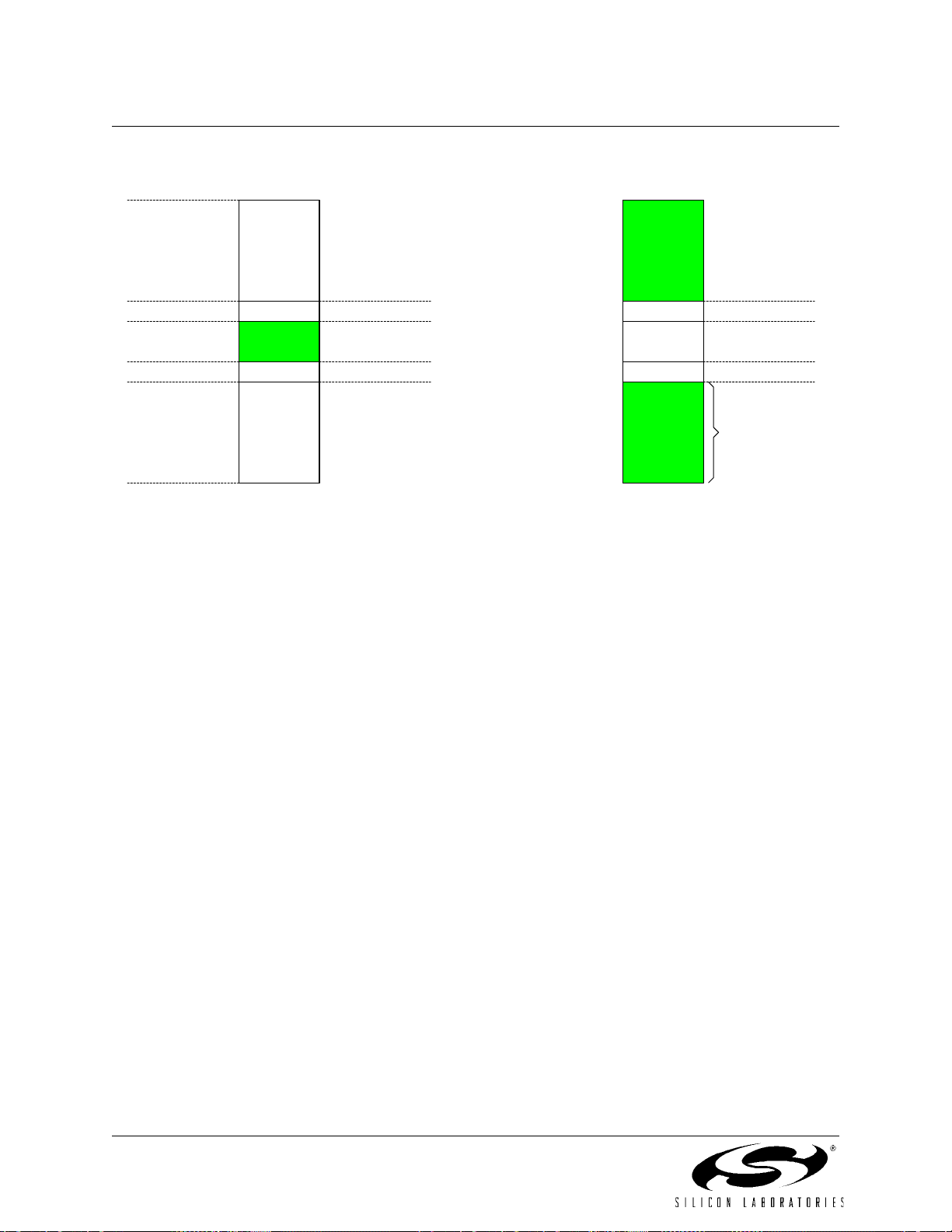
C8051F120/1/2/3/4/5/6/7
C8051F130/1/2/3
Input Voltage
(AD0.0 - AGND)
REF x (4095/4096)
REF x (512/4096)
REF x (256/4096)
0
ADC Data
Word
0xFFF0
0x2010
0x2000
0x1FF0
0x1010
0x1000
0x0FF0
0x0000
AD0WINT
not affected
ADC0LTH:ADC0LTL
AD0WINT=1
ADC0GTH:ADC0GTL
AD0WINT
not affected
Input Voltage
(AD0.0 - AGND)
REF x (4095/4096)
0
ADC Data
Word
0xFFF0
0x2010
0x2000
0x1FF0
0x1010
0x1000
0x0FF0
0x0000
AD0WINT=1
ADC0GTH:ADC0GTL
AD0WINT
not affected
ADC0LTH:ADC0LTL
AD0WINT=1
Figure 5.8. 12-Bit ADC0 Window Interrupt Example: Left Justified Single-Ended
Data
70 Rev. 1.4

C8051F120/1/2/3/4/5/6/7
C8051F130/1/2/3
Input Voltage
(AD0.0 - AD0.1)
REF x (2047/2048)
REF x (256/2048)
REF x (-1/2048)
-REF
ADC Data
Word
0x7FF0
0x1010
0x1000
0x0FF0
0x0000
0xFFF0
0xFFE0
0x8000
AD0WINT
not affected
ADC0LTH:ADC0LTL
AD0WINT=1
ADC0GTH:ADC0GTL
AD0WINT
not affected
Given:
AMX0SL = 0x00, AMX0CF = 0x01,
AD0LJST = ‘1’,
ADC0LTH:ADC0LTL = 0x1000,
ADC0GTH:ADC0GTL = 0xFFF0.
An ADC0 End of Conversion will cause an
ADC0 Window Compare Interrupt (AD0WINT
= ‘1’) if the resulting ADC0 Data Word is
< 0x1000 and > 0xFFF0. (2s-complement
math.)
Input Voltage
(AD0.0 - AD0.1)
REF x (2047/2048)
REF x (256/2048)
REF x (-1/2048)
-REF
ADC Data
Word
0x7FF0
0x1010
0x1000
0x0FF0
0x0000
0xFFF0
0xFFE0
0x8000
AD0WINT=1
ADC0GTH:ADC0GTL
AD0WINT
not affected
ADC0LTH:ADC0LTL
AD0WINT=1
Given:
AMX0SL = 0x00, AMX0CF = 0x01,
AD0LJST = ‘1’,
ADC0LTH:ADC0LTL = 0xFFF0,
ADC0G TH:ADC0GTL = 0x1000.
An ADC0 End of Conversion will cause an
ADC0 Window Compare Interrupt (AD0WINT
= ‘1’) if the resulting ADC0 Data Word is
< 0xFFF0 or > 0x1000. (2s-complement math.)
Figure 5.9. 12-Bit ADC0 Window Interrupt Example: Left Justified Differential Data
Rev. 1.4 71

C8051F120/1/2/3/4/5/6/7
C8051F130/1/2/3
Table 5.1. 12-Bit ADC0 Electrical Characteristics (C8051F120/1/4/5)
V
= 3.0 V, AV+ = 3.0 V, VREF = 2.40 V (REFBE = 0), PGA Gain = 1, –40 to +85 °C unless otherwise specified.
DD
Parameter Conditions Min Typ Max Units
DC Accuracy
Resolution 12 bits
Integral Nonlinearity — — ±1 LSB
Differential Nonlinearity Guaranteed Monotonic — — ±1 LSB
Offset Error — –3±1 — LSB
Full Scale Error Differential mode — –7±3 — LSB
Offset Temperature Coefficient — ±0.25 — ppm/°C
Dynamic Performance (10 kHz sine-wave input, 0 to 1 dB below Full Scale, 100 ksps
Signal-to-Noise Plus Distortion 66 — — dB
Total Harmonic Distortion
Up to the 5
th
harmonic
—–75— dB
Spurious-Free Dynamic Range — 80 — dB
Conversion Rate
SAR Clock Frequency — — 2.5 MHz
Conversion Time in SAR Clocks 16 — — clocks
Track/Hold Acquisition Time 1.5 — — µs
Throughput Rate — — 100 ksps
Analog Inputs
Input Voltage Range Single-ended operation 0 — VREF V
*Common-mode Voltage Range Differential operation AGND — AV+ V
Input Capacitance — 10 — pF
Temperature Sensor
Linearity
Offset (Temp = 0 °C) — 776 — mV
Offset Error
Slope — 2.86 — mV / °C
Slope Error
Power Supply Current
(AV+ supplied to ADC)
1
1, 2
2
(Temp = 0 °C) — ±8.5 — mV
Power Specifications
Operating Mode, 100 ksps
—±0.2— °C
— ±0.034 — mV / °C
—450900 µA
Power Supply Rejection — ±0.3 — mV/V
Notes:
1.
Includes ADC offset, gain, and linearity variations.
2. Represents one standard deviation from the mean.
72 Rev. 1.4

C8051F120/1/2/3/4/5/6/7
C8051F130/1/2/3
6. ADC0 (10-Bit ADC, C8051F122/3/6/7 and C8051F13x Only)
The ADC0 subsystem for the C8051F122/3/6/7 and C8051F13x consists of a 9-channel, configurable analog multiplexer (AMUX0), a programmable gain amplifier (PGA0), and a 100 ksps, 10-bit successiveapproximation-register ADC with integrated track-and-hold and Programmable Window Detector (see
block diagram in Figure 6.1). The AMUX0, PGA0, Data Conv ersion Modes, and Window Detect or are all
configurable under software control via the Special Function Registers shown in Figure 6.1. The voltage
reference used by ADC0 is selected as described in
ADC0 subsystem (ADC0, track-and-hold and PGA0) is enabled only when the AD0EN bit in the ADC0
Control register (ADC0CN) is set to logic 1. The ADC0 subsystem is in low power shutdown when this bit is
logic 0.
TEMP
+
+
+
+
-
9-to-1
AMUX
(SE or
DIFF)
X
AD0EN
AV+
+
-
AGND
AIN0.0
AIN0.1
AIN0.2
AIN0.3
AIN0.4
AIN0.5
AIN0.6
AIN0.7
SENSOR
AGND
Section “9. Voltage Reference” on page 113. The
ADC0LTLADC0LTHADC0GTLADC0GTH
20
AV+
REF
SYSCLK
Comb.
Logic
10
AD0WINT
10-Bit
SAR
ADC
AD0CM
10
Start Conversion
ADC0L ADC0H
00
01
10
11
AD0BUSY (W)
Timer 3 Overflow
CNVSTR0
Timer 2 Overflow
AIN01IC
AIN23IC
AIN45IC
AIN67IC
AMX0CF
AMX0SL
AMX0AD0
AMX0AD1
AMX0AD2
AMX0AD3
AD0SC3
AD0SC4
ADC0CF
AD0SC1
AD0SC2
AMP0GN2
AD0SC0
AMP0GN0
AMP0GN1
AD0INT
AD0TM
AD0EN
ADC0CN
AD0WINT
AD0CM0
AD0CM1
AD0BUSY
AD0LJST
AD0CM
Figure 6.1. 10-Bit ADC0 Functional Block Diagram
6.1. Analog Multiplexer and PGA
Eight of the AMUX channels are available for external measurements while the ninth channel is internally
connected to an on-chip temperature sensor (temperature transfer function is shown in Figure 6.2). AMUX
input pairs can be programmed to operate in either differential or single-ended mode. This allows the user
to select the best measurement technique for each input channel, and even accommodates mode
changes "on-the-fly". The AMUX defaults to all single-ended inputs upon reset. There are two registers
associated with the AMUX: the Channel Selection register AMX0SL (SFR Definition 6.2), and the Configuration register AMX0CF (SFR Definition 6.1). The table in SFR Definition 6.2 shows AMUX functionality by
channel, for each possible configuration. The PGA amplifies the AMUX output signal by an amount determined by the states of the AMP0GN2-0 bits in the ADC0 Configuration register, ADC0CF (SFR Definition
6.3). The PGA can be software-programmed for gains of 0.5, 2, 4, 8 or 16. Gain defaults to unity on reset.
Rev. 1.4 73
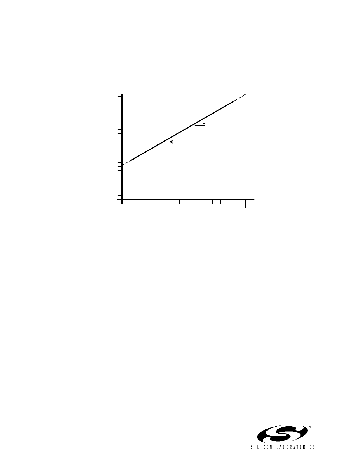
C8051F120/1/2/3/4/5/6/7
C8051F130/1/2/3
The Temperature Sensor transfer function is shown in Figure 6.2. The output voltage (V
input when the Temperature Sensor is selected by bits AMX0AD3-0 in register AMX0SL; this voltage will
be amplified by the PGA according to the user-programm ed PGA settings. Typical values for the Slope and
Offset parameters can be found in Table 6.1.
Slope (V / deg C)
Offset (V at 0 Celsius)
) is the PGA
TEMP
Voltage
V
= (Slope x TempC) + Offset
TEMP
Temp
= (V
C
0-50 50 100
- Offset) / Slope
TEMP
Temperature (Celsius)
Figure 6.2. Typical Temperature Sensor Transfer Function
74 Rev. 1.4

C8051F120/1/2/3/4/5/6/7
C8051F130/1/2/3
6.2. ADC Modes of Operation
ADC0 has a maximum conversion speed of 100 ksps. The ADC0 conversion clock is derived from the system clock divided by the value held in the ADCSC bits of register ADC0CF.
6.2.1. Starting a Conversion
A conversion can be initiated in one of four ways, depending on the programmed states of the ADC0 Start
of Conversion Mode bits (AD0CM1, AD0CM0) in ADC0CN. Conversions may be initiated by:
1. Writing a ‘1’ to the AD0BUSY bit of ADC0CN;
2. A Timer 3 overflow (i.e. timed continuous conversions);
3. A rising edge detected on the external ADC convert start signal, CNVSTR0;
4. A Timer 2 overflow (i.e. timed continuous conversions).
The AD0BUSY bit is set to logic 1 during conversion and restored to logic 0 when conversion is complete.
The falling edge of AD0BUSY triggers an interrupt (when enabled) and sets the AD0INT interrupt flag
(ADC0CN.5). Converted data is available in the ADC0 data word MSB and LSB registers, ADC0H, ADC0 L.
Converted data can be either left or right justified in the ADC0H:ADC0L register pair (see example in
Figure 6.5) depending on the programmed state of the AD0LJST bit in the ADC0CN register.
When initiating conversions by writ ing a ‘1’ to AD0BUSY, the AD0INT bit should be polled to determine
when a conversion has completed (ADC0 interrupts may also be used). The recommended polling procedure is shown below.
Step 1. Write a ‘0’ to AD0INT;
Step 2. Write a ‘1’ to AD0BUSY;
Step 3. Poll AD0INT for ‘1’;
Step 4. Process ADC0 data.
When CNVSTR0 is used as a conversion start source, it must be enabled in th e crossbar, and the corresponding pin must be set to open-drain, high-impedance mode (see
page 235
for more details on Port I/O configuration).
Section “18. Port Input/Output” on
Rev. 1.4 75

C8051F120/1/2/3/4/5/6/7
C8051F130/1/2/3
6.2.2. Tracking Modes
The AD0TM bit in register ADC0CN controls the ADC0 track-and-hold mode. In its default state, the ADC0
input is continuously tracked when a conversion is not in progress. When the AD0TM bit is logic 1, ADC0
operates in low-power track-and-hold mode. In this mode, each conversion is preceded by a tracking
period of 3 SAR clocks (after the start-of-conversion signal). When the CNVSTR0 signal is used to initiate
conversions in low-power tracking mode, ADC0 tra cks only when CNVSTR0 is low; conversion begins on
the rising edge of CNVSTR0 (see Figure 6.3). Tracking can also be disabled (shutdown) when the entire
chip is in low power standby or sleep modes. Low-power track-and-hold mode is also useful when AMUX
or PGA settings are frequently changed, to ensure that settling time requirements are met (see
“6.2.3. Settling Time Requirements” on page 77
).
A. ADC Timing for External Trigger Source
CNVSTR0
(AD0CM[1:0]=10)
12345678910111213141516
SAR Clocks
Section
ADC0TM=1
ADC0TM=0
Timer 2, Timer 3 Overflow;
Write '1' to AD0BUSY
(AD0CM[1:0]=00, 01, 11)
SAR Clocks
ADC0TM=1
SAR Clocks
ADC0TM=0
Figure 6.3. ADC0 Track and Conversion Example Timing
Low Power
or Convert
Track Or Convert Convert Track
Track Convert Low Power Mode
B. ADC Timing for Internal Trigger Sources
1234567891011121314151617 18 19
Low Power
or Convert
Track or
Convert
Track Convert Low Powe r M ode
12345678910111213141516
Convert Track
76 Rev. 1.4
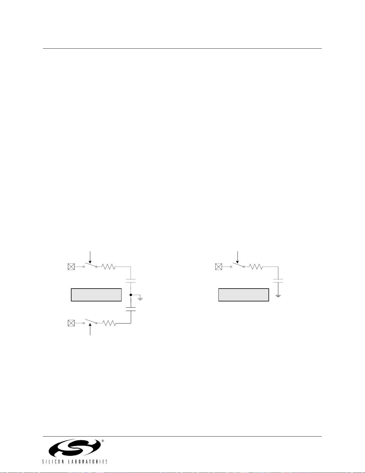
C8051F120/1/2/3/4/5/6/7
C8051F130/1/2/3
6.2.3. Settling Time Requirements
A minimum tracking time is required before an accurate conversion can be performed. This tracking time is
determined by the ADC0 MUX resistance, the ADC0 sampling capacitance, any external source re sistance, and the accuracy required for the conversion. Figure 6.4 shows the equivalent ADC0 input circuits
for both Differential and Single-ended modes. Notice that the equivalent time constant for both input circuits is the same. The required settling time for a given settling accuracy (
Equation 6.1. When measuring the Temperature Sensor output,
R
TOTAL
minimum settling time of 1.5 µs is required after any MUX or PGA selection. Note that in low-power tracking mode, three SAR clocks are used for tracking at the start of ever y conversion. For most application s,
these three SAR clocks will meet the tracking requirements.
n
2
⎛⎞
------ -
t
×ln=
⎝⎠
SA
R
TOTALCSAMPLE
Equation 6.1. ADC0 Settling Time Requirements
Where:
SA is the settling accuracy, given as a fraction of an LSB (for example, 0.25 to settle within 1/4 LSB)
t is the required settling time in seconds
R
n is the ADC resolution in bits (10).
is the sum of the ADC0 MUX resistance and any external source resistance.
TOTAL
SA) may be approximated by
reduces to R
. An absolute
MUX
AIN0.x
AIN0.y
Differential Mode
MUX Select
R
= 5k
MUX
RC
= R
Input
MUX Select
* C
MUX
SAMPLE
R
= 5k
MUX
Figure 6.4. ADC0 Equivalent Input Circuits
C
C
SAMPLE
SAMPLE
= 10pF
= 10pF
Single-Ended Mode
MUX Select
AIN0.x
RC
Input
= R
MUX
R
* C
MUX
SAMPLE
= 5k
C
SAMPLE
= 10pF
Rev. 1.4 77

C8051F120/1/2/3/4/5/6/7
C8051F130/1/2/3
SFR Definition 6.1. AMX0CF: AMUX0 Configuration
SFR Page:
SFR Address:
R/W R/W R/W R/W R/W R/W R/W R/W Reset Value
Bit7 Bit6 Bit5 Bit4 Bit3 Bit2 Bit1 Bit0
Bits7–4: UNUSED. Read = 0000b; Write = don’t care.
Bit3: AIN67IC: AIN0.6, AIN0.7 Input Pair Configuration Bit.
Bit2: AIN45IC: AIN0.4, AIN0.5 Input Pair Configuration Bit.
Bit1: AIN23IC: AIN0.2, AIN0.3 Input Pair Configuration Bit.
Bit0: AIN01IC: AIN0.0, AIN0.1 Input Pair Configuration Bit.
Note: The ADC0 Data Word is in 2’s complement format for channels configured as differential.
0
0xBA
- - - - AIN67IC AIN45IC AIN23IC AIN01IC 00000000
0: AIN0.6 and AIN0.7 are independent single-ended input s.
1: AIN0.6, AIN0.7 are (respectively) +, - differen tial input pair.
0: AIN0.4 and AIN0.5 are independent single-ended input s.
1: AIN0.4, AIN0.5 are (respectively) +, - differen tial input pair.
0: AIN0.2 and AIN0.3 are independent single-ended input s.
1: AIN0.2, AIN0.3 are (respectively) +, - differen tial input pair.
0: AIN0.0 and AIN0.1 are independent single-ended input s.
1: AIN0.0, AIN0.1 are (respectively) +, - differen tial input pair.
78 Rev. 1.4
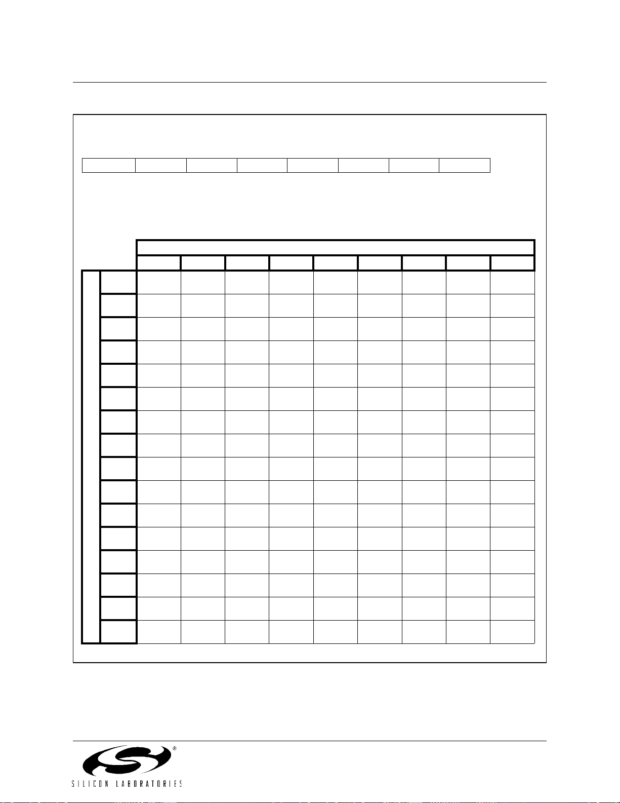
C8051F120/1/2/3/4/5/6/7
C8051F130/1/2/3
SFR Definition 6.2. AMX0SL: AMUX0 Channel Select
SFR Page:
SFR Address:
R/W R/W R/W R/W R/W R/W R/W R/W Reset Value
0
0xBB
- - - - AMX0AD3 AMX0AD2 AMX0AD1 AMX0AD0 00000000
Bit7 Bit6 Bit5 Bit4 Bit3 Bit2 Bit1 Bit0
Bits7–4: UNUSED. Read = 0000b; Write = don’t care.
Bits3–0: AMX0AD3–0: AMX0 Address Bits.
0000-1111b: ADC Inputs selected per chart below.
AMX0AD3-0
0000 0001 0010 0011 0100 0101 0110 0111 1xxx
AIN0.0 AIN0.1 AIN0.2 AIN0.3 AIN0.4 AIN0.5 AIN0.6 AIN0.7
+(AIN0.0)
–(AIN0.1)
AIN0.0 AIN0.1
+(AIN0.0)
–(AIN0.1)
AIN0.0 AIN0.1 AIN0.2 AIN0.3
+(AIN0.0)
–(AIN0.1)
AIN0.0 AIN0.1
+(AIN0.0)
–(AIN0.1)
AIN0.0 AIN0.1 AIN0.2 AIN0.3 AIN0.4 AIN0.5
+(AIN0.0)
–(AIN0.1)
AIN0.0 AIN0.1
+(AIN0.0)
–(AIN0.1)
AIN0.0 AIN0.1 AIN0.2 AIN0.3
+(AIN0.0)
–(AIN0.1)
AIN0.0 AIN0.1
+(AIN0.0)
–(AIN0.1)
AIN0.2 AIN0.3 AIN0.4 AIN0.5 AIN0.6 AIN0.7
+(AIN0.2)
–(AIN0.3)
+(AIN0.2)
–(AIN0.3)
AIN0.2 AIN0.3
+(AIN0.2)
–(AIN0.3)
+(AIN0.2)
–(AIN0.3)
AIN0.2 AIN0.3 AIN0.4 AIN0.5
+(AIN0.2)
–(AIN0.3)
+(AIN0.2)
–(AIN0.3)
AIN0.2 AIN0.3
+(AIN0.2)
–(AIN0.3)
+(AIN0.2)
–(AIN0.3)
AIN0.4 AIN0.5 AIN0.6 AIN0.7
AIN0.4 AIN0.5 AIN0.6 AIN0.7
+(AIN0.4)
–(AIN0.5)
+(AIN0.4)
–(AIN0.5)
+(AIN0.4)
–(AIN0.5)
+(AIN0.4)
–(AIN0.5)
AIN0.4 AIN0.5
AIN0.4 AIN0.5
+(AIN0.4)
–(AIN0.5)
+(AIN0.4)
–(AIN0.5)
+(AIN0.4)
–(AIN0.5)
+(AIN0.4)
–(AIN0.5)
AIN0.6 AIN0.7
AIN0.6 AIN0.7
AIN0.6 AIN0.7
AIN0.6 AIN0.7
+(AIN0.6)
–(AIN0.7)
+(AIN0.6)
–(AIN0.7)
+(AIN0.6)
–(AIN0.7)
+(AIN0.6)
–(AIN0.7)
+(AIN0.6)
–(AIN0.7)
+(AIN0.6)
–(AIN0.7)
+(AIN0.6)
–(AIN0.7)
+(AIN0.6)
–(AIN0.7)
AMX0CF Bits 3-0
0000
0001
0010
0011
0100
0101
0110
0111
1000
1001
1010
1011
1100
1101
1110
1111
TEMP
SENSOR
TEMP
SENSOR
TEMP
SENSOR
TEMP
SENSOR
TEMP
SENSOR
TEMP
SENSOR
TEMP
SENSOR
TEMP
SENSOR
TEMP
SENSOR
TEMP
SENSOR
TEMP
SENSOR
TEMP
SENSOR
TEMP
SENSOR
TEMP
SENSOR
TEMP
SENSOR
TEMP
SENSOR
Rev. 1.4 79

C8051F120/1/2/3/4/5/6/7
C8051F130/1/2/3
SFR Definition 6.3. ADC0CF: ADC0 Configuration
SFR Page:
SFR Address:
R/W R/W R/W R/W R/W R/W R/W R/W Reset Value
AD0SC4 AD0SC3 AD0SC2 AD0SC1 AD0SC0 AMP0GN2 AMP0GN1 AMP0GN0 11111000
Bit7 Bit6 Bit5 Bit4 Bit3 Bit2 Bit1 Bit0
Bits7–3: AD0SC4–0: ADC0 SAR Conversion Clock Period Bits.
Bits2–0: AMP0GN2–0: ADC0 Internal Amplifier Gain (PGA).
0
0xBC
SAR Conversion clock is derived from sy stem clock by the following equation, where
AD0SC refers to the 5-bit value held in AD0SC4-0, a nd CLK
SAR clock (Note: the ADC0 SAR Conversion Clock should be less than or equal to
2.5 MHz).
SYSCLK
AD0SC
When the AD0SC bits are equal to 00000b, the SAR Conversion clock is equal to SYSCLK
to facilitate faster ADC conversions at slower SYSCLK speeds.
000: Gain = 1
001: Gain = 2
010: Gain = 4
01 1: Gain = 8
10x: Gain = 16
11x: Gain = 0.5
-------------------------------2 C× LK
SAR0
1–= AD0SC 00000b>()
refers to the desired ADC0
SAR0
80 Rev. 1.4

C8051F120/1/2/3/4/5/6/7
C8051F130/1/2/3
SFR Definition 6.4. ADC0CN: ADC0 Control
SFR Page:
SFR Address:
R/W R/W R/W R/W R/W R/W R/W R/W Reset Value
AD0EN AD0TM AD0INT AD0BUSY AD0CM1 AD0CM0 AD0WINT AD0LJST 00000000
Bit7 Bit6 Bit5 Bit4 Bit3 Bit2 Bit1 Bit0
Bit7: AD0EN: ADC0 Enable Bit.
Bit6: AD0TM: ADC Track Mode Bit.
Bit5: AD0INT: ADC0 Conversion Complete Interrupt Flag.
Bit4: AD0BUSY: ADC0 Busy Bit.
Bits3–2: AD0CM1–0: ADC0 Start of Conversion Mode Select.
Bit1: AD0WINT: ADC0 Window Compare Interrupt Flag.
Bit0: AD0LJST: ADC0 Left Justify Select.
0
0xE8 (bit addressable)
0: ADC0 Disabled. ADC0 is in low-power shutdown.
1: ADC0 Enabled. ADC0 is active and ready for data conversions.
0: When the ADC is enabled, tracking is continuous unless a conversion is in process.
1: Tracking Defined by ADCM1-0 bits.
This flag must be cleared by software.
0: ADC0 has not completed a data conversion since the last time this flag was cleared.
1: ADC0 has completed a data conversion.
Read:
0: ADC0 Conversion is complete or a conversion is not currently in progre ss. AD0INT is set
to logic 1 on the falling edge of AD0BUSY.
1: ADC0 Conversion is in progress.
Write:
0: No Effect.
1: Initiates ADC0 Conversion if AD0CM1-0 = 00b.
If AD0TM = 0:
00: ADC0 conversion initiated on every write of ‘1’ to AD0BUSY.
01: ADC0 conversion initiated on overflow of Timer 3.
10: ADC0 conversion initiated on rising edge of external CNVSTR0.
11: ADC0 conversion initiated on overflow of Timer 2.
If AD0TM = 1:
00: Tracking starts with the write of ‘1’ to AD0BUSY and lasts for 3 SAR clocks, followed by
conversion.
01: Tracking started by the overflow of Timer 3 and lasts for 3 SAR clocks, followed by conversion.
10: ADC0 tracks only when CNVSTR0 input is logic low; conversion starts on rising
CNVSTR0 edge.
11: Tracking started by the overflow of Timer 2 and lasts for 3 SAR clocks, followed by conversion.
This bit must be cleared by software.
0: ADC0 Window Comparison Data match has not occur red sin ce th is flag wa s last clear ed .
1: ADC0 Window Comparison Data match has occurr ed.
0: Data in ADC0H:ADC0L registers are right-justified.
1: Data in ADC0H:ADC0L registers are left-justified.
Rev. 1.4 81

C8051F120/1/2/3/4/5/6/7
C8051F130/1/2/3
SFR Definition 6.5. ADC0H: ADC0 Data Word MSB
SFR Page:
SFR Address:
R/W R/W R/W R/W R/W R/W R/W R/W Reset Value
Bit7 Bit6 Bit5 Bit4 Bit3 Bit2 Bit1 Bit0
Bits7–0: ADC0 Data Word High-Order Bits.
0
0xBF
For AD0LJST = 0: Bits 7–4 are the sign extension of Bit3 . Bits 3–0 are the upp er 4 bits of the
10-bit ADC0 Data Word.
For AD0LJST = 1: Bits 7–0 are the most-significant bits of the 10-bit ADC0 Data Word.
SFR Definition 6.6. ADC0L: ADC0 Data Word LSB
SFR Page:
SFR Address:
R/W R/W R/W R/W R/W R/W R/W R/W Reset Value
Bit7 Bit6 Bit5 Bit4 Bit3 Bit2 Bit1 Bit0
Bits7–0: ADC0 Data Word Low-Order Bits.
0
0xBE
00000000
For AD0LJST = 0: Bits 7–0 are the lower 8 bits of the 10-bit ADC0 Data Word.
For AD0LJST = 1: Bits 7–4 are the lower 4 bits of the 10-bit ADC0 Data Word. Bits 3–0 will
always read ‘0’.
00000000
82 Rev. 1.4

C8051F120/1/2/3/4/5/6/7
C8051F130/1/2/3
10-bit ADC0 Data Word appear s in the ADC0 Data Word Registers as follows:
ADC0H[1:0]:ADC0L[7:0], if AD0LJST = 0
(ADC0H[7:2] will be sign-extension of ADC0H.1 for a differential reading, otherwise
=
000000b).
ADC0H[7:0]:ADC0L[7:6], if AD0LJST = 1
(ADC0L[5:0] = 00b).
Example: ADC0 Data Word Conversion Map , AIN0 .0 Input in Single-Ended Mode
(AMX0CF = 0x00, AMX0SL = 0x00)
AIN0.0–AGND
(Volts)
VREF x (1023/1024) 0x03FF 0xFFC0
VREF / 2 0x0200 0x8000
VREF x (511/1024) 0x01FF 0x7FC0
0 0x0000 0x0000
Example: ADC0 Data Word Conversion Map, AIN0.0 -AIN0.1 Differential Input Pair
(AMX0CF = 0x01, AMX0SL = 0x00)
AIN0.0–AIN0.1
(Volts)
VREF x (511/512) 0x01FF 0x7FC0
VREF / 2 0x0100 0x4000
VREF x (1/512) 0x0001 0x0040
0 0x0000 0x0000
–VREF x (1/512) 0xFFFF (–1d) 0xFFC0
–VREF / 2 0xFF00 (–256d) 0xC000
–VREF 0xFE00 (–512d) 0x8000
For AD0LJST = 0:
Code Vin
× 2n×=
ADC0H:ADC0L
(AD0LJST = 0)
ADC0H:ADC0L
(AD0LJST = 0)
Gain
---------------
VREF
ADC0H:ADC0L
(AD0LJST = 1)
ADC0H:ADC0L
(AD0LJST = 1)
; ‘n’ = 10 for Single-Ended; ‘n’= 9 for Differential.
Figure 6.5. ADC0 Data Word Example
Rev. 1.4 83

C8051F120/1/2/3/4/5/6/7
C8051F130/1/2/3
6.3. ADC0 Programmable Window Detector
The ADC0 Programmable Window Detector continuously compares th e ADC0 output to user-pr ogra mme d
limits, and notifies the system when an out-of-boun d condi tion is detected. This is especially effective in an
interrupt-driven system, saving code space and CPU bandwidth while delivering faster system response
times. The window detector interrupt flag (AD0WINT in ADC0CN) can also be used in polled mode. The
high and low bytes of the reference words are loaded into the ADC0 Greater-Than and ADC0 Less-Than
registers (ADC0GTH, ADC0GTL, ADC0LTH, and ADC0LTL). Reference comparisons are shown starting
on page 87. Notice that the window detector flag can be asserted when th e measur ed data is inside or outside the user-programmed limits, depending on the programming of the ADC0GTx and ADC0LTx registers.
SFR Definition 6.7. ADC0GTH: ADC0 Greater-Than Data High Byte
SFR Page:
SFR Address:
R/W R/W R/W R/W R/W R/W R/W R/W Reset Value
Bit7 Bit6 Bit5 Bit4 Bit3 Bit2 Bit1 Bit0
Bits7–0: High byte of ADC0 Greater-Than Data Word.
0
0xC5
SFR Definition 6.8. ADC0GTL: ADC0 Greater-Than Data Low Byte
SFR Page:
SFR Address:
R/W R/W R/W R/W R/W R/W R/W R/W Reset Value
Bit7 Bit6 Bit5 Bit4 Bit3 Bit2 Bit1 Bit0
Bits7–0: Low byte of ADC0 Greater-Tha n Da ta Word.
0
0xC4
11111111
11111111
84 Rev. 1.4

C8051F120/1/2/3/4/5/6/7
C8051F130/1/2/3
SFR Definition 6.9. ADC0LTH: ADC0 Less-Than Data High Byte
SFR Page:
SFR Address:
R/W R/W R/W R/W R/W R/W R/W R/W Reset Value
Bit7 Bit6 Bit5 Bit4 Bit3 Bit2 Bit1 Bit0
Bits7–0: High byte of ADC0 Less-Than Data Word.
0
0xC7
00000000
SFR Definition 6.10. ADC0LTL: ADC0 Less-Than Data Low Byte
SFR Page:
SFR Address:
R/W R/W R/W R/W R/W R/W R/W R/W Reset Value
Bit7 Bit6 Bit5 Bit4 Bit3 Bit2 Bit1 Bit0
Bits7–0: Low byte of ADC0 Less-Than Data Word.
0
0xC6
00000000
Rev. 1.4 85

C8051F120/1/2/3/4/5/6/7
C8051F130/1/2/3
Input Voltage
(AD0.0 - AGND)
REF x (1023/1024)
REF x (512/1024)
REF x (256/1024)
0
ADC Data
Word
0x03FF
0x0201
0x0200
0x01FF
0x0101
0x0100
0x00FF
0x0000
ADWINT
not affected
ADC0LTH:ADC0LTL
ADWINT=1
ADC0GTH:ADC0GTL
ADWINT
not affected
Given:
AMX0SL = 0x00, AMX0CF = 0x00
AD0LJST = ‘0’,
ADC0LTH:ADC0LTL = 0x0200,
ADC0GTH:ADC0GTL = 0x0100.
An ADC0 End of Conversion will cause an
ADC0 Window Compare Interrupt (AD0WINT
= ‘1’) if the resulting ADC0 Data Word is
< 0x0200 and > 0x0100.
Input Voltage
(AD0.0 - AGND)
REF x (1023/1024)
REF x (512/1024)
REF x (256/1024)
0
ADC Data
Word
0x03FF
0x0201
0x0200
0x01FF
0x0101
0x0100
0x00FF
0x0000
ADWINT=1
ADC0GTH:ADC0GTL
ADWINT
not affected
ADC0LTH:ADC0LTL
ADWINT=1
Given:
AMX0SL = 0x00, AMX0CF = 0x00,
AD0LJST = ‘0’,
ADC0LTH:ADC0LTL = 0x0100,
ADC0G TH:ADC0GTL = 0x0200.
An ADC0 End of Conversion will cause an
ADC0 Window Compare Interrupt (AD0WINT
= ‘1’) if the resulting ADC0 Data Word is
> 0x0200 or < 0x0100.
Figure 6.6. 10-Bit ADC0 Window Interrupt Example: Right Justified Single-Ended
Data
86 Rev. 1.4

C8051F120/1/2/3/4/5/6/7
C8051F130/1/2/3
Input Voltage
(AD0.0 - AD0.1)
REF x (511/512)
REF x (256/512)
REF x (-1/512)
-REF
ADC Data
Word
0x01FF
0x0101
0x0100
0x00FF
0x0000
0xFFFF
0xFFFE
0xFE00
ADWINT
not affected
ADC0LTH:ADC0LTL
ADWINT=1
ADC0GTH:ADC0GTL
ADWINT
not affected
Given:
AMX0SL = 0x00, AMX0CF = 0x01,
AD0LJST = ‘0’,
ADC0LTH:ADC0LTL = 0x0100,
ADC0GTH:ADC0GTL = 0xFFFF.
An ADC0 End of Conversion will cause an
ADC0 Window Compare Interrupt (AD0WINT
= ‘1’) if the resulting ADC0 Data Word is
< 0x0100 and > 0xFFFF. (In 2s-complement
math, 0xFFFF = -1.)
Input Voltage
(AD0.0 - AD0.1)
REF x (511/512)
REF x (256/512)
REF x (-1/512)
-REF
ADC Data
Word
0x01FF
0x0101
0x0100
0x00FF
0x0000
0xFFFF
0xFFFE
0xFE00
ADWINT=1
ADC0GTH:ADC0GTL
ADWINT
not affected
ADC0LTH:ADC0LTL
ADWINT=1
Given:
AMX0SL = 0x00, AMX0CF = 0x01,
AD0LJST = ‘0’,
ADC0LTH:ADC0LTL = 0xFFFF,
ADC0G TH:ADC0GTL = 0x0100.
An ADC0 End of Conversion will cause an
ADC0 Window Compare Interrupt (AD0WINT
= ‘1’) if the resulting ADC0 Data Word is
< 0xFFFF or > 0x0100. (In 2s-complement
math, 0xFFFF = -1.)
Figure 6.7. 10-Bit ADC0 Window Interrupt Example: Right Justified Differential
Data
Rev. 1.4 87

C8051F120/1/2/3/4/5/6/7
C8051F130/1/2/3
Input Voltage
(AD0.0 - AG ND)
REF x (1023/1024)
REF x (512/1024)
REF x (256/1024)
0
ADC Data
Word
0xFFC0
0x8040
0x8000
0x7FC0
0x4040
0x4000
0x3FC0
0x0000
ADWINT
not affected
ADC0LTH:ADC0LTL
ADWINT=1
ADC0GTH:ADC0GTL
ADWINT
not affected
Given:
AMX0SL = 0x00, AMX0CF = 0x00,
AD0LJST = ‘1’,
ADC0LTH:ADC0LTL = 0x2000,
ADC0GTH:ADC0GTL = 0x1000.
An ADC0 End of Conversion will cause an
ADC0 Window Compare Interrupt (AD0WINT
= ‘1’) if the resulting ADC0 Data Word is
< 0x2000 and > 0x1000.
Input Voltage
(AD0.0 - AGND)
REF x (1023/1024)
REF x (512/1024)
REF x (256/1024)
0
ADC Data
Word
0xFFC0
0x8040
0x8000
0x7FC0
0x4040
0x4000
0x3FC0
0x0000
ADWINT=1
ADC0GTH:ADC0GTL
ADWINT
not affected
ADC0LTH:ADC0LTL
ADWINT=1
Given:
AMX0SL = 0x00, AMX0CF = 0x00,
AD0LJST = ‘1’
ADC0LTH:ADC0LTL = 0x1000,
ADC0G TH:ADC0GTL = 0x2000.
An ADC0 End of Conversion will cause an
ADC0 Window Compare Interrupt (AD0WINT
= ‘1’) if the resulting ADC0 Data Word is
< 0x1000 or > 0x2000.
Figure 6.8. 10-Bit ADC0 Window Interrupt Example: Left Justified Single-Ended
Data
88 Rev. 1.4
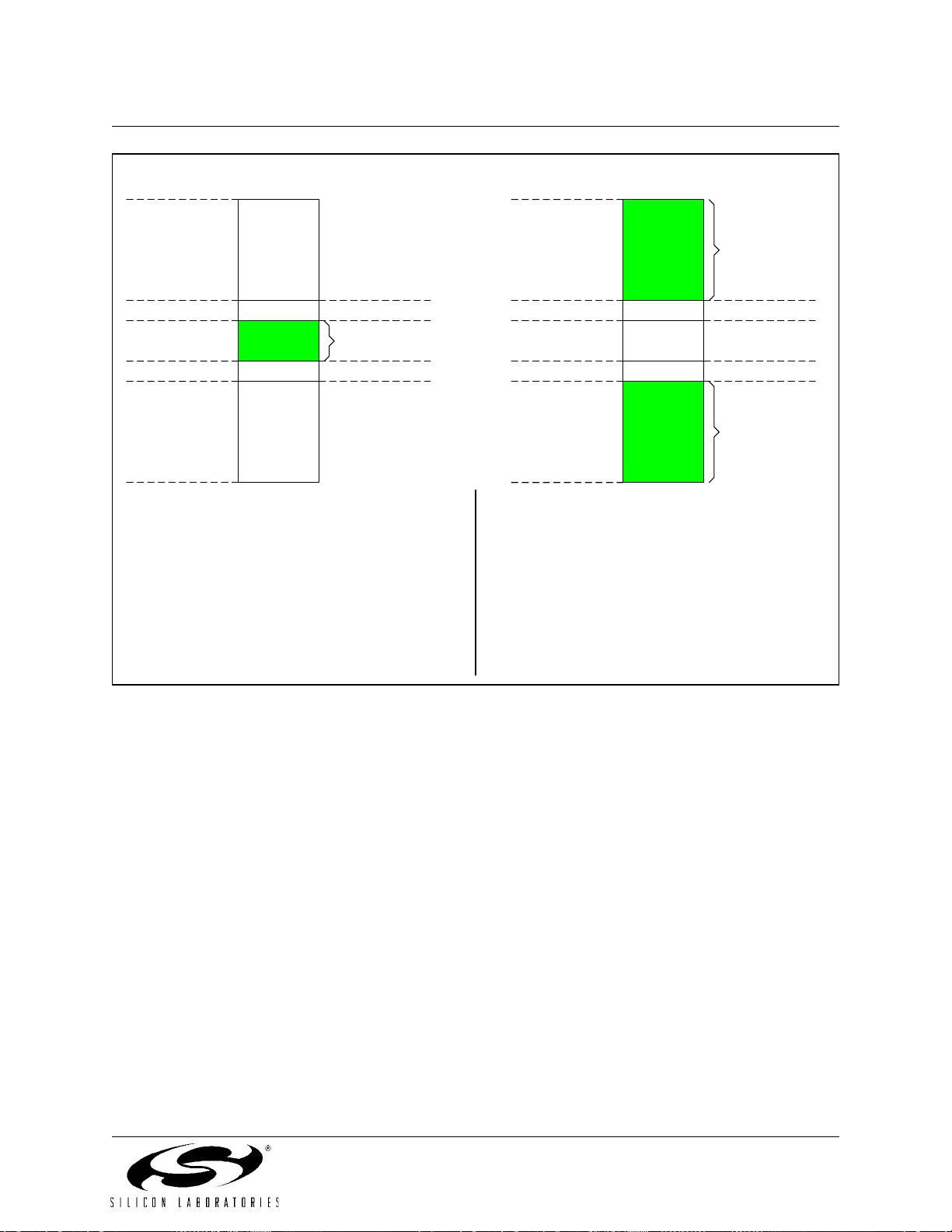
C8051F120/1/2/3/4/5/6/7
C8051F130/1/2/3
Input Voltage
(AD0.0 - AD0.1)
REF x (511/512)
REF x (128/512)
REF x (-1/512)
-REF
ADC Data
Word
0x7FC0
0x2040
0x2000
0x1FC0
0x0000
0xFFC0
0xFF80
0x8000
ADWINT
not affected
ADC0LTH:ADC0LTL
ADWINT=1
ADC0GTH:ADC0GTL
ADWINT
not affected
Given:
AMX0SL = 0x00, AMX0CF = 0x01,
AD0LJST = ‘1’,
ADC0LTH:ADC0LTL = 0x2000,
ADC0GTH:ADC0GTL = 0xFFC0.
An ADC0 End of Conversion will cause an
ADC0 Window Compare Interrupt (AD0WINT
= ‘1’) if the resulting ADC0 Data Word is
< 0x2000 and > 0xFFC0. (2s-complement
math.)
Input Voltage
(AD0.0 - AD0.1)
REF x (511/512)
REF x (128/512)
REF x (-1/512)
-REF
ADC Data
Word
0x7FC0
0x2040
0x2000
0x1FC0
0x0000
0xFFC0
0xFF80
0x8000
ADWINT=1
ADC0GTH:ADC0GTL
ADWINT
not affected
ADC0LTH:ADC0LTL
ADWINT=1
Given:
AMX0SL = 0x00, AMX0CF = 0x01,
AD0LJST = ‘1’,
ADC0LTH:ADC0LTL = 0xFFC0,
ADC0G TH:ADC0GTL = 0x2000.
An ADC0 End of Conversion will cause an
ADC0 Window Compare Interrupt (AD0WINT
= ‘1’) if the resulting ADC0 Data Word is
< 0xFFC0 or > 0x2000. (2s-complement
math.)
Figure 6.9. 10-Bit ADC0 Window Interrupt Example: Left Justified Differential Data
Rev. 1.4 89
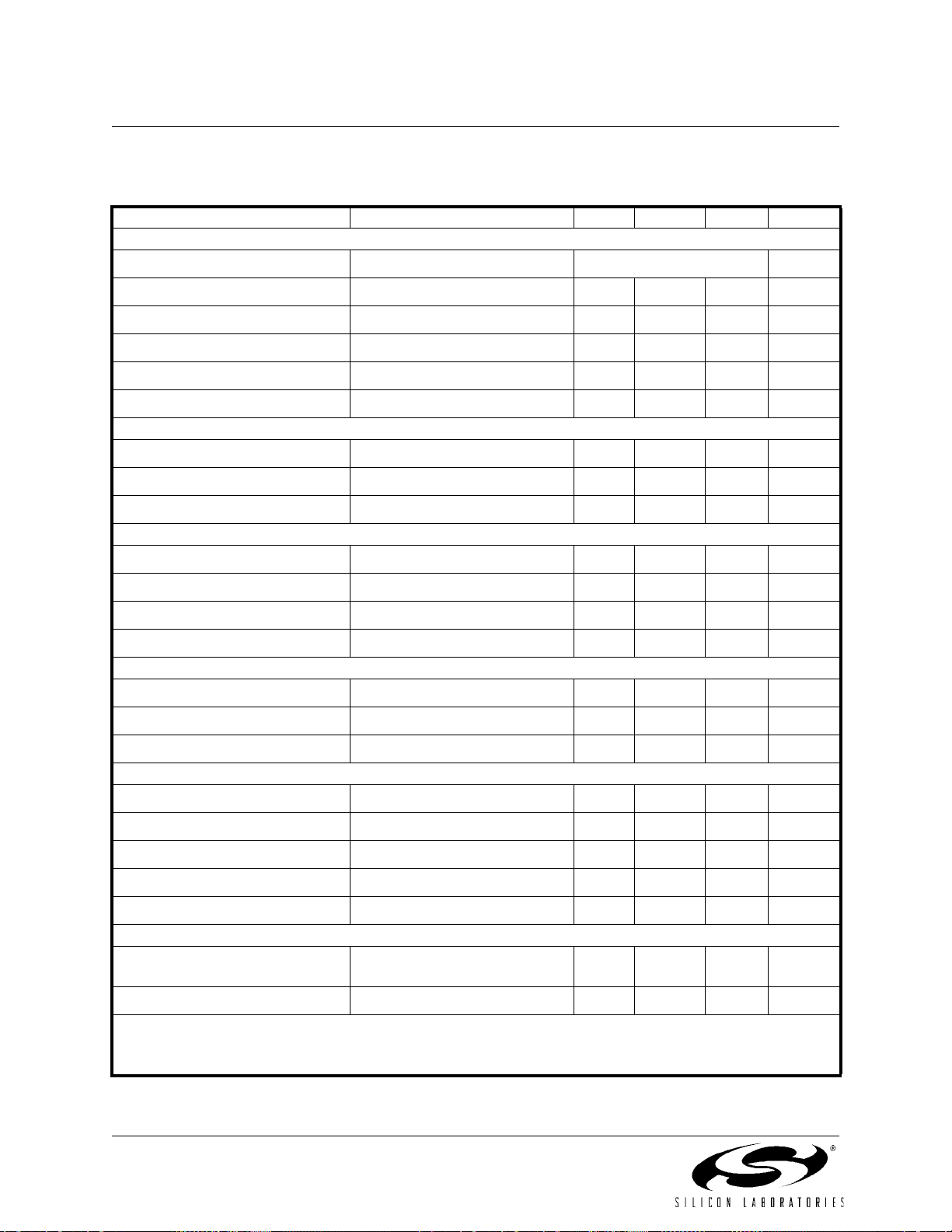
C8051F120/1/2/3/4/5/6/7
C8051F130/1/2/3
Table 6.1. 10-Bit ADC0 Electrical Characteristics (C8051F122/3/6/7 and C8051F13x)
V
= 3.0 V, AV+ = 3.0 V, VREF = 2.40 V (REFBE = 0), PGA Gain = 1, –40 to +85 °C unless otherwise specified.
DD
Parameter Conditions Min Typ Max Units
DC Accuracy
Resolution 10 bits
Integral Nonlinearity — — ±1 LSB
Differential Nonlinearity Guaranteed Monotonic — — ±1 LSB
Offset Error — ±0.5 — LSB
Full Scale Error Differential mode — –1.5±0.5 — LSB
Offset Temperature Coefficient — ±0.25 — ppm/°C
Dynamic Performance (10 kHz sine-wave input, 0 to 1 dB below Full Scale, 100 ksps
Signal-to-Noise Plus Distortion 59 — — dB
Total Harmonic Distortion
Spurious-Free Dynamic Range — 80 — dB
SAR Clock Frequency — — 2.5 MHz
Up to the 5
th
harmonic
Conversion Rate
— –70 — dB
Conversion Time in SAR Clocks 16 — — clocks
Track/Hold Acquisition Time 1.5 — — µs
Throughput Rate — — 100 ksps
Analog Inputs
Input Voltage Range Single-ended operation 0 — VREF V
*Common-mode Voltage Range Differential operation AGND — AV+ V
Input Capacitance — 10 — pF
Temperature Sensor
Linearity
Offset (Temp = 0 °C) — 776 — mV
Offset Error
Slope — 2.86 — mV/°C
Slope Error
Power Supply Current
(AV+ supplied to ADC)
Power Supply Rejection — ±0.3 — mV/V
Notes:
1
1,2
2
1.
Includes ADC offset, gain, and linearity variations.
2. Represents one standard deviation from the mean.
(Temp = 0 °C) — ±8.5 — mV
Power Specifications
Operating Mode, 100 ksps
—±0.2— °C
— ±0.034 — mV/°C
— 450 900 µA
90 Rev. 1.4
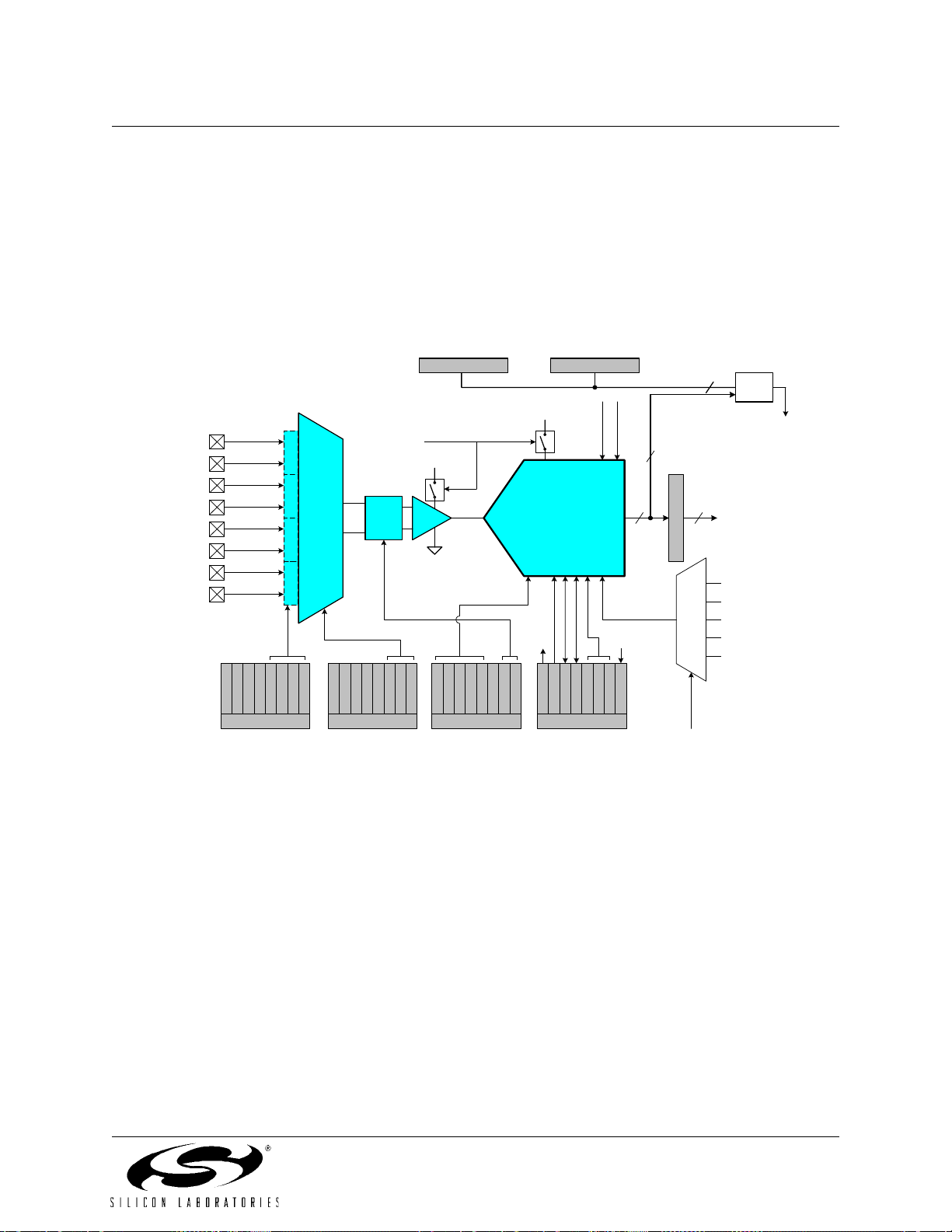
C8051F120/1/2/3/4/5/6/7
C8051F130/1/2/3
7. ADC2 (8-Bit ADC, C8051F12x Only)
The C8051F12x devices include a second ADC peripheral (ADC2), which consists of an 8-chan nel, configurable analog multiplexer , a programmable gain amplifier, and a 500 ksps, 8-bit successive-approximationregister ADC with integrated track-and-hold (see block diagram in Figure 7.1). ADC2 is fully configurable
under software control via the Special Function Registers shown in Figure 7.1. The ADC2 subsystem (8-bit
ADC, track-and-hold and PGA) is enabled only when the AD2EN bit in the ADC2 Control register
(ADC2CN) is set to logic 1. The ADC2 subsystem is in low power shutdown when this bit is logic 0. The
voltage reference used by ADC2 is selected as described in
page 113
.
AIN2.0 (P1.0)
AIN2.1 (P1.1)
AIN2.2 (P1.2)
AIN2.3 (P1.3)
AIN2.4 (P1.4)
AIN2.5 (P1.5)
AIN2.6 (P1.6)
AIN2.7 (P1.7)
PIN67IC
AMX2CF
PIN45IC
+
-
+
-
+
-
+
-
8-to-1
AMUX
PIN01IC
PIN23IC
AD2EN
AV+
+
X
-
AD2SC0
ADC
AMP2GN0
AMP2GN1
AGND
AMX2AD0
AMX2AD1
AMX2AD2
AMX2SL ADC2CN
AD2SC3
AD2SC4
ADC2CF
AD2SC1
AD2SC2
Section “9. Voltage Reference” on
AV+
ADC2LTHADC2GTH
REF
SYSCLK
8
16
Comp
8-Bit
SAR
AD2TM
AD2EN
AD2INT
AD2BUSY
Start Conversion
AD2CM
AD2WINT
AD2CM0
AD2CM1
AD2CM2
8
8
ADC2
000
001
010
011
1xx
AD2CM
Write to AD2BUSY
Timer 3 Overflow
CNVSTR2
Timer 2 Overflow
Write to AD0BUSY
(synchronized with
ADC0)
Dig
AD2WINT
Figure 7.1. ADC2 Functional Block Diagram
7.1. Analog Multiplexer and PGA
Eight ADC2 channels are available for measurement, as selected by the AMX2SL register (see SFR Definition 7.2). The PGA amplifies the ADC2 output signal by an amount determined by the states of the
AMP2GN2-0 bits in the ADC2 Configuration r e gist er, ADC2CF (SFR Definition 7. 3) . T h e PG A c an be s oftware-programmed for gains of 0.5, 1, 2, or 4. Gain defaults to 0.5 on reset.
Important Note: AIN2 pins also function a s Port 1 I/O pins, and must be configured as analog input s when
used as ADC2 inputs. To configure an AIN2 pin for analog input, set to ‘0’ the corresponding bit in register
P1MDIN. Port 1 pins selected as analog inputs are skipped by the Digital I/O Crossbar. See
“18.1.5. Configuring Port 1 Pins as Analog Inputs” on page 240
for more information on configuring
the AIN2 pins.
Rev. 1.4 91
Section

C8051F120/1/2/3/4/5/6/7
C8051F130/1/2/3
7.2. ADC2 Modes of Operation
ADC2 has a maximum conversion speed of 500 ksps. The ADC2 conversion clock (SAR2 clock) is a
divided version of the system clock, determined by the AD2SC bits in the ADC2CF register. The maximum
ADC2 conversion clock is 6 MHz.
7.2.1. Starting a Conversion
A conversion can be initiated in one of five w ays, de pending on the programmed states of the ADC2 Start
of Conversion Mode bits (AD2CM2-0) in ADC2CN. Conversions may be initiated by:
1. Writing a ‘1’ to the AD2BUSY bit of ADC2CN;
2. A Timer 3 overflow (i.e. timed continuous conversions);
3. A rising edge detected on the external ADC convert start signal, CNVSTR2;
4. A Timer 2 overflow (i.e. timed continuous conversions);
5. Writing a ‘1’ to the AD0BUSY of register ADC0CN (initiate conversion of ADC2 and ADC0 with
a single software command).
During conversion, the AD2BUSY bit is set to logic 1 and restored to 0 when conversion is complete. The
falling edge of AD2BUSY triggers an interrupt (when enabled) and sets the interrupt flag in ADC2CN. Converted data is available in the ADC2 data word, ADC2.
When a conversion is initiated by writing a ‘1’ to AD2BUSY , it is recommended to poll AD2INT to determine
when the conversion is complete. The recommended procedure is:
Step 1. Write a ‘0’ to AD2INT;
Step 2. Write a ‘1’ to AD2BUSY;
Step 3. Poll AD2INT for ‘1’;
Step 4. Process ADC2 data.
When CNVSTR2 is used as a conversion start source, it must be enabled in th e crossbar, and the corresponding pin must be set to open-drain, high-impedance mode (see
page 235
for more details on Port I/O configuration).
Section “18. Port Input/Output” on
7.2.2. Tracking Modes
The AD2TM bit in register ADC2CN controls the ADC2 track-and-hold mode. In its default state, the ADC2
input is continuously tracked, except when a conversion is in progress. When the AD2TM bit is logic 1,
ADC2 operates in low-power track-and-hold mode. In this mode, each conversion is preceded by a tracking period of 3 SAR clocks (after the start-of-conversion signal). When the CNV STR2 signal is us ed to initiate conversions in low-power tracking mode, ADC2 tracks only when CNVSTR2 is low; conversion
begins on the rising edge of CNVSTR2 (see Figure 7.2). Tracking can also be disabled (shutdown) when
the entire chip is in low power standby or sleep modes. Low-power Track-and-Hold mode is also useful
when AMUX or PGA settings are frequently changed, due to the settling time requirements described in
Section “7.2.3. Settling Time Requirements” on page 94.
92 Rev. 1.4
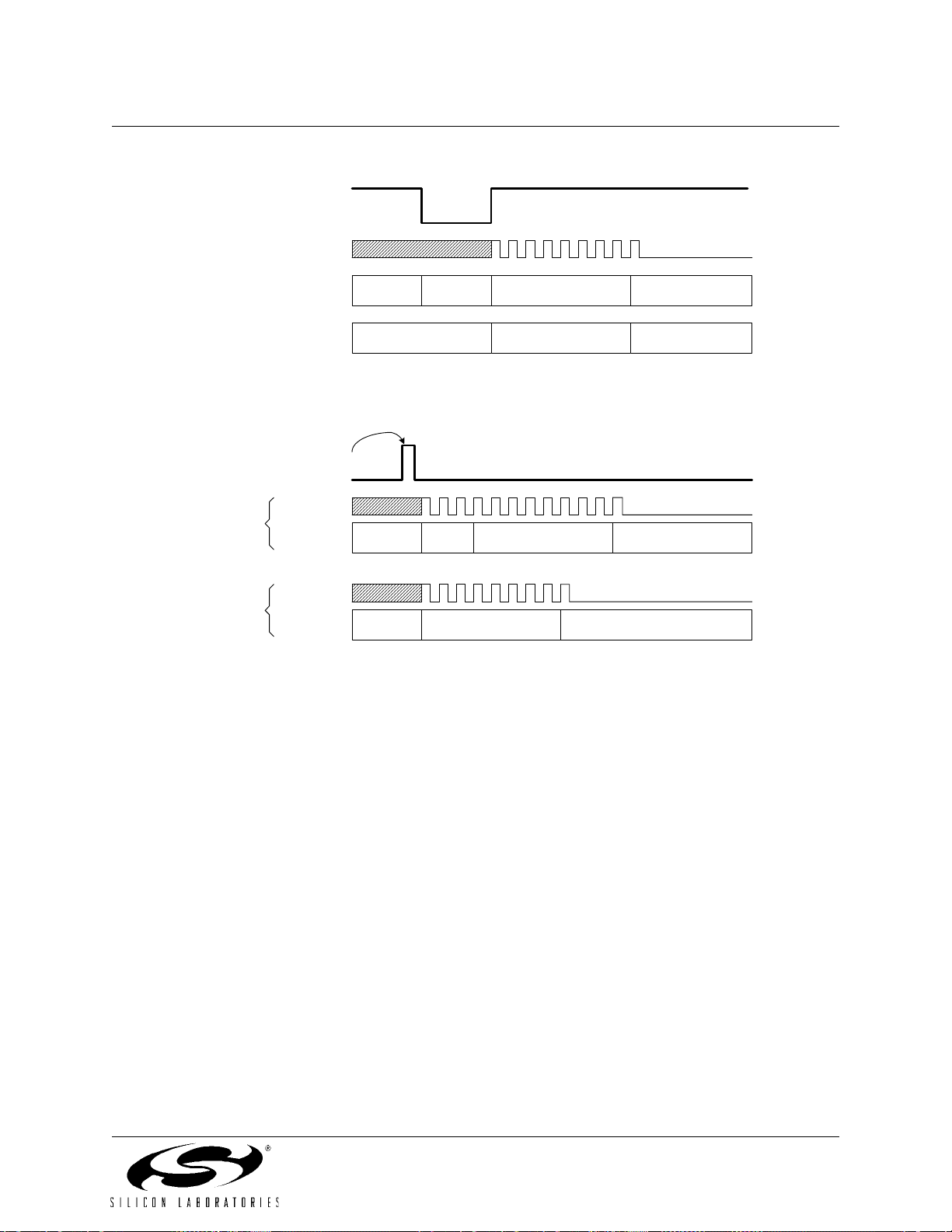
CNVSTR2
(AD2CM[2:0]=010)
SAR Clocks
C8051F120/1/2/3/4/5/6/7
C8051F130/1/2/3
A. ADC Timing for External Trigger Source
123456789
AD2TM=1
Write '1' to AD2BUSY,
Timer 3 Overflow,
Timer 2 Overflow,
Write '1' to AD0BUSY
(AD2CM[2:0]=000, 001, 011, 1xx)
SAR Clocks
AD2TM=1
SAR Clocks
AD2TM=0
Figure 7.2. ADC2 Track and Conversion Example Timing
Low Power
or Convert
Track or Convert Convert TrackAD2TM=0
Track Convert Low Power Mode
B. ADC Timing for Internal Trigger Source
123456789101112
Low Power
or Convert
Track or
Convert
Track Convert Low Power Mode
123456789
Convert Track
Rev. 1.4 93

C8051F120/1/2/3/4/5/6/7
C8051F130/1/2/3
94 Rev. 1.4

C8051F120/1/2/3/4/5/6/7
C8051F130/1/2/3
SFR Definition 7.1. AMX2CF: AMUX2 Configuration
SFR Page:
SFR Address:
R/W R/W R/W R/W R/W R/W R/W R/W Reset Value
Bit7 Bit6 Bit5 Bit4 Bit3 Bit2 Bit1 Bit0
Bits7–4: UNUSED. Read = 0000b; Write = don’t care.
Bit3: PIN67IC: AIN2.6, AIN2.7 Input Pair Configuration Bit.
Bit2: PIN45IC: AIN2.4, AIN2.5 Input Pair Configuration Bit.
Bit1: PIN23IC: AIN2.2, AIN2.3 Input Pair Configuration Bit.
Bit0: PIN01IC: AIN2.0, AIN2.1 Input Pair Configuration Bit.
Note: The ADC2 Data Word is in 2’s complement format for channels configured as differential.
2
0xBA
- - - - PIN67IC PIN45IC PIN23IC PIN01IC 00000000
0: AIN2.6 and AIN2.7 are independent single-ended inputs.
1: AIN2.6 and AIN2.7 are (respectively) +, – differential input pair.
0: AIN2.4 and AIN2.5 are independent single-ended inputs.
1: AIN2.4 and AIN2.5 are (respectively) +, – differential input pair.
0: AIN2.2 and AIN2.3 are independent single-ended inputs.
1: AIN2.2 and AIN2.3 are (respectively) +, – differential input pair.
0: AIN2.0 and AIN2.1 are independent single-ended inputs.
1: AIN2.0 and AIN2.1 are (respectively) +, – differential input pair.
Rev. 1.4 95

C8051F120/1/2/3/4/5/6/7
C8051F130/1/2/3
SFR Definition 7.2. AMX2SL: AMUX2 Channel Select
SFR Page:
SFR Address:
R/W R/W R/W R/W R/W R/W R/W R/W Reset Value
2
0xBB
- - - - AMX2AD2 AMX2AD1 AMX2AD0 00000000
Bit7 Bit6 Bit5 Bit4 Bit3 Bit2 Bit1 Bit0
Bits7–3: UNUSED. Read = 00000b; Write = don’t care.
Bits2–0: AMX2AD2–0: AMX2 Address Bits.
000-111b: ADC Inputs selected per chart below.
AMX2AD2–0
000 001 010 011 100 101 110 111
0000
0001
0010
0011
0100
0101
0110
0111
1000
1001
AMX2CF Bits 3–0
1010
1011
1100
1101
1110
1111
AIN2.0 AIN2.1 AIN2.2 AIN2.3 AIN2.4 AIN2.5 AIN2.6 AIN2.7
+(AIN2.0)
–(AIN2.1)
AIN2.0 AIN2.1
+(AIN2.0)
–(AIN2.1)
AIN2.0 AIN2.1 AIN2.2 AIN2.3
+(AIN2.0)
–(AIN2.1)
AIN2.0 AIN2.1
+(AIN2.0)
–(AIN2.1)
AIN2.0 AIN2.1 AIN2.2 AIN2.3 AIN2.4 AIN2.5
+(AIN2.0)
–(AIN2.1)
AIN2.0 AIN2.1
+(AIN2.0)
–(AIN2.1)
AIN2.0 AIN2.1 AIN2.2 AIN2.3
+(AIN2.0)
–(AIN2.1)
AIN2.0 AIN2.1
+(AIN2.0)
–(AIN2.1)
AIN2.2 AIN2.3 AIN2.4 AIN2.5 AIN2.6 AIN2.7
+(AIN2.2)
–(AIN2.3)
+(AIN2.2)
–(AIN2.3)
AIN2.2 AIN2.3
+(AIN2.2)
–(AIN2.3)
+(AIN2.2)
–(AIN2.3)
AIN2.2 AIN2.3 AIN2.4 AIN2.5
+(AIN2.2)
–(AIN2.3)
+(AIN2.2)
–(AIN2.3)
AIN2.2 AIN2.3
+(AIN2.2)
–(AIN2.3)
+(AIN2.2)
–(AIN2.3)
AIN2.4 AIN2.5 AIN2.6 AIN2.7
AIN2.4 AIN2.5 AIN2.6 AIN2.7
+(AIN2.4)
–(AIN2.5)
+(AIN2.4)
–(AIN2.5)
+(AIN2.4)
–(AIN2.5)
+(AIN2.4)
–(AIN2.5)
AIN2.4 AIN2.5
AIN2.4 AIN2.5
+(AIN2.4)
–(AIN2.5)
+(AIN2.4)
–(AIN2.5)
+(AIN2.4)
–(AIN2.5)
+(AIN2.4)
–(AIN2.5)
AIN2.6 AIN2.7
AIN2.6 AIN2.7
AIN2.6 AIN2.7
AIN2.6 AIN2.7
+(AIN2.6)
–(AIN2.7)
+(AIN2.6)
–(AIN2.7)
+(AIN2.6)
–(AIN2.7)
+(AIN2.6)
–(AIN2.7)
+(AIN2.6)
–(AIN2.7)
+(AIN2.6)
–(AIN2.7)
+(AIN2.6)
–(AIN2.7)
+(AIN2.6)
–(AIN2.7)
96 Rev. 1.4

C8051F120/1/2/3/4/5/6/7
A
C8051F130/1/2/3
SFR Definition 7.3. ADC2CF: ADC2 Configuration
SFR Page:
SFR Address:
R/W R/ W R/W R/W R/ W R/W R/W R /W Reset Value
AD2SC4 AD2SC3 AD2SC2 AD2SC1 AD2SC0 - AMP2GN1 AMP2GN0 11111000
Bit7 Bit6 Bit5 Bit4 Bit3 Bit2 Bit1 Bit0
Bits7–3: AD2SC4–0: ADC2 SAR Conversion Clock Period Bits.
Bit2: UNUSED. Read = 0b; Write = don’t care.
Bits1–0: AMP2GN1–0: ADC2 Internal Amplifier Gain (PGA).
2
0xBC
SAR Conversion clock is derived from sy stem clock by the following equation, where
AD2SC refers to the 5-bit value held in AD2SC4–0, and CLK
ADC2 SAR clock (Note: the ADC2 SAR Conversion Clock should be less than or equal to
6MHz).
SYSCLK
D2SC
00: Gain = 0.5
01: Gain = 1
10: Gain = 2
11: Gain = 4
---------------------- -
CLK
SAR2
1–=
refers to the desired
SAR2
Rev. 1.4 97

C8051F120/1/2/3/4/5/6/7
C8051F130/1/2/3
SFR Definition 7.4. ADC2CN: ADC2 Control
SFR Page:
SFR Address:
R/W R/W R/W R/W R/W R/W R/W R/W Reset Value
AD2EN AD2TM AD2INT AD2BUSY AD2CM2 AD2CM1 AD2CM0 AD2WINT 00000000
Bit7 Bit6 Bit5 Bit4 Bit3 Bit2 Bit1 Bit0
Bit7: AD2EN: ADC2 Enable Bit.
Bit6: AD2TM: ADC2 Track Mode Bit.
Bit5: AD2INT: ADC2 Conversion Complete Interrupt Flag.
Bit4: AD2BUSY: ADC2 Busy Bit.
Bits3–1: AD2CM2–0: ADC2 Start of Conversion Mode Select.
Bit0: AD2WINT: ADC2 Window Compare Interrupt Fla g.
2
0xE8 (bit addressable)
0: ADC2 Disabled. ADC2 is in low-power shutdown.
1: ADC2 Enabled. ADC2 is active and ready for data conversions.
0: Normal Track Mode: When ADC2 is enabled, tracking is continuous unless a conversion
is in process.
1: Low-power Track Mode: Tracking Defined by AD2CM2-0 bits (see below).
This flag must be cleared by software.
0: ADC2 has not completed a data conversion since the last time this flag was cleared .
1: ADC2 has completed a data conversion.
Read:
0: ADC2 Conversion is complete or a conversion is not currently in progress. AD2INT is set
to logic 1 on the falling edge of AD2BUSY.
1: ADC2 Conversion is in progress.
Write:
0: No Effect.
1: Initiates ADC2 Conversion if AD2CM2-0 = 000b
AD2TM = 0:
000: ADC2 conversion initiated on every write of ‘1’ to AD2BUSY.
001: ADC2 conversion initiated on overflow of Timer 3.
010: ADC2 conversion initiated on rising edge of external CNVSTR2.
01 1: ADC2 conversion initiated on overflow of Timer 2.
1xx: ADC2 conversion initiated on write of ‘1’ to AD0BUSY (synchronized with ADC0 software-commanded conversions).
AD2TM = 1:
000: Tracking initiated on write of ‘1’ to AD2BUSY for 3 SAR2 clocks, followed by conversion.
001: Tracking initiated on overflow of Timer 3 for 3 SAR2 clocks, followed by conversion.
010: ADC2 tracks only when CNVSTR2 input is logic low; conversion starts on rising
CNVSTR2 edge.
011: Tracking initiated on overflow of Timer 2 for 3 SAR2 clocks, followed by conversion.
1xx: Tracking initiated on write of ‘1’ to AD0BUSY an d lasts 3 SAR2 clocks, followed by conversion.
This bit must be cleared by software.
0: ADC2 Window Comparison Data match has not occurred since this flag was last cleared.
1: ADC2 Window Comparison Data match has occurred.
98 Rev. 1.4

C8051F120/1/2/3/4/5/6/7
C8051F130/1/2/3
SFR Definition 7.5. ADC2: ADC2 Data Word
SFR Page:
SFR Address:
R/W R/W R/W R/W R/W R/W R/W R/W Reset Value
Bit7 Bit6 Bit5 Bit4 Bit3 Bit2 Bit1 Bit0
Bits7–0: ADC2 Data Word.
2
0xBE
Single-Ended Example:
8-bit ADC Data Word appears in the ADC2 Data Word Register as follows:
Example: ADC2 Data Word Conversion Map, Single-Ended AIN2.0 Inpu t
(AMX2CF = 0x00; AMX2SL = 0x00)
AIN2.0–AGND
(Volts)
VREF * (255/256) 0xFF
VREF * (128/256) 0x80
VREF * (64/256) 0x40
00x00
ADC2
00000000
Gain
Code Vin
Differential Example:
8-bit ADC Data Word appears in the ADC2 Data Word Register as follows:
Example: ADC2 Data Word Conversion Map, Differential AIN2.0-AIN2.1 Input
(AMX2CF = 0x01; AMX2SL = 0x00)
AIN2.0–AIN2.1
(Volts)
VREF * (127/128) 0x7F
VREF * (64/128) 0x40
00x00
–VREF * (64/128) 0xC0 (-64d)
–VREF * (128/128) 0x80 (-128d)
Code Vin
---------------
× 256×=
VREF
Gain
------------------------ -
× 256×=
2 V× REF
ADC2
Figure 7.4. ADC2 Data Word Example
Rev. 1.4 99
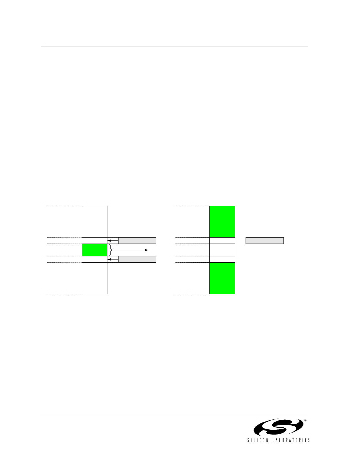
C8051F120/1/2/3/4/5/6/7
C8051F130/1/2/3
7.3. ADC2 Programmable Window Detector
The ADC2 Programmable Window Detector continuously compares th e ADC2 output to user-pr ogra mme d
limits, and notifies the system when a desired condition is detected. This is especially effective in an interrupt-driven system, saving code space and CPU bandwidth while delivering faster system response times.
The window detector interrupt flag (AD2WINT in register ADC2CN) can also be used in polled mode. The
ADC2 Greater-Than (ADC2GT) and Less-Than (ADC2LT) registers hold the comparison values. Example
comparisons for Differential and Single-ended modes are shown in Figure 7.6 and Figure 7.5, respectively.
Notice that the window detector flag can be programmed to indicate when measured data is inside or outside of the user-programmed limits, depending on the contents of the ADC2LT and ADC2GT registers.
7.3.1. Window Detector In Single-Ended Mode
Figure 7.5 shows two example window comparisons for Single-ended mode, with ADC2LT = 0x20 and
ADC2GT = 0x10. Notice that in Single-ended mode, the codes vary from 0 to VREF*(255/256) and are
represented as 8-bit unsigned integers. In the left example, an AD2WINT interrupt will be generated if the
ADC2 conversion word (ADC2) is within the range defined by ADC2GT and ADC2LT
(if 0x10
of the range defined by ADC2GT and ADC2LT (if ADC2
< ADC2 < 0x20). In the right example, and AD2WINT interrupt will be generated if ADC2 is outside
< 0x10 or ADC2 > 0x20).
Input Voltage
(AIN2.x - AG N D)
REF x (255/256)
REF x (32/256)
REF x (16/256)
0
0xFF
0x21
0x20
0x1F
0x11
0x10
0x0F
0x00
AD2WINT
not affected
ADC2LT
ADC2GT
AD2WINT
not affected
AD2WINT=1
Input Voltage
(AIN2.x - AGND)
REF x (255/256)
REF x (32/256)
REF x (16/256)
0
0xFF
0x21
0x20
0x1F
0x11
0x10
0x0F
0x00
Figure 7.5. ADC2 Window Compare Examples, Single-Ended Mode
ADC2GT
AD2WINT
not affected
100 Rev. 1.4
 Loading...