

Page 1
C8051F020/1/2/3
8K ISP FLASH MCU Family
ANALOG PERIPHERALS
- SAR ADC
• 12-Bit (C8051F020/1)
• 10-Bit (C8051F022/3)
• ± 1 LSB INL
• Programmable Throughput up to 100 ksps
• Up to 8 External Inputs; Programmable as Single-Ended or
Differential
• Programmable Amplifier Gain: 16, 8, 4, 2, 1, 0.5
• Data-Dependent Windowed Interrupt Generator
• Built-in Temperature Sensor (± 3°C)
- 8-bit ADC
• Programmable Throughput up to 500 ksps
• 8 External Inputs
• Programmable Amplifier Gain: 4, 2, 1, 0.5
- Two 12-bit DACs
• Can Synchronize Outputs to T im ers for Jitter-Free Wave-
form Generation
- Two Analog Comparators
- Voltage Reference
- Precision VDD Monitor/Brown-Out Detector
ON-CHIP JTAG DEBUG & BOUNDARY SCAN
- On-Chip Debug Circuitry Facilitates Full- Speed, Non-
Intrusive In-Circuit/In-System Debugging
- Provides Breakpoints, Single-Stepping, Watchpoints,
Stack Monitor; Inspect/Modify Memory and Registers
- Superior Performance to Emulation Systems Using ICE-
Chips, Target Pods, and Sockets
- IEEE1149.1 Compliant Boundary Scan
- Low-Cost, Complete Development Kit
HIGH SPEED 8051 µC CORE
- Pipelined Instruction Architecture; Executes 70% of
Instruction Set in 1 or 2 System Clocks
- Up to 25 MIPS Throughput with 25 MHz Clock
- 22 Vectored Interrupt Sources
MEMORY
- 4352 Bytes Internal Data RAM (4k + 256)
- 64k Bytes FLASH; In-System programmable in 512-byte
Sectors
- External 64k Byte Data Memory Interface (programma-
ble multiplexed or non-multiplexed modes)
DIGITAL PERIPHERALS
- 8 Byte-Wide Port I/O (C8051F020/2); 5V tolerant
- 4 Byte-Wide Port I/O (C8051F021/3); 5V tolerant
- Hardware SMBus™ (I
Two
UART Serial Ports Available Concurrently
2
C™ Compatible), SPI™, and
- Programmable 16-bit Counter/Timer Array with
5
Capture/Compare Modules
- 5 General Purpose 16-bit Counter/Timers
- Dedicated Watch-Dog Timer; Bi-directional Reset Pin
CLOCK SOURCES
- Internal Programmable Oscillator: 2-to-16 MHz
- External Oscillator: Crystal, RC, C, or Clock
- Real-Time Clock Mode using Timer 3 or PCA
SUPPLY VOLTAGE .......................... 2.7V TO 3.6V
- Typical Operating Current: 10 mA @ 20 MHz
- Multiple Power Saving Sleep and Shutdown Modes
100-Pin TQFP and 64-Pin TQFP Packages Available
Temperature Range: -40°C to +85°C
ANALOG PERIPHERALS
TEMP
AMUX
12-Bit
DAC
12-Bit
DAC
SENSOR
PGA
VREF
AMUX
10/12-bit
100ksps
ADC
PGA
+
-
VOLTAGE
COMPARATORS
500ksps
+
-
8-bit
ADC
HIGH-SPEED CONTROLLER CORE
8051 CPU
(25MIPS)
22
INTERRUPTS
64KB
ISP FLASH
DEBUG
CIRCUITRY
CIRCUIT
DIGITAL I/O
UART0
UART1
SMBus
SPI Bus
PCA
Timer 0
Timer 1
Timer 2
Timer 3
Timer 4
4352 B
SRAM
CLOCK
CROSSBAR
64 pin
SANITY
CONTROL
Port 0
Port 1
Port 2
Port 3
Port 4
Port 5
External Memory Interface
Port 6
Port 7
100 pin
JTAG
Preliminary Rev. 1.4 12/03 Copyright © 2003 by Silicon Laboratories C8051F020/1/2/3-DS14
This information applies to a product under development. Its characteristics and specifications are subject to change without notice.
Page 2

C8051F020/1/2/3
Notes
2 Rev. 1.4
Page 3

C8051F020/1/2/3
TABLE OF CONTENTS
1. SYSTEM OVERVIEW .........................................................................................................17
1.1. CIP-51™ Microcontroller Core ......................................................................................22
1.1.1. Fully 8051 Compatible ..........................................................................................22
1.1.2. Improved Throughput ............................................................................................22
1.1.3. Additional Features ................................................................................................23
1.2. On-Chip Memory ............................................................................................................24
1.3. JTAG Debug and Boundary Scan ...................................................................................25
1.4. Programmable Digital I/O and Crossbar .........................................................................26
1.5. Programmable Counter Array .........................................................................................27
1.6. Serial Ports.......................................................................................................................27
1.7. 12-Bit Analog to Digital Converter .................................................................................28
1.8. 8-Bit Analog to Digital Converter ...................................................................................29
1.9. Comparators and DACs................................................................................................... 30
2. ABSOLUTE MAXIMUM RATINGS..................................................................................31
3. GLOBAL DC ELECTRICAL CHARACTERISTICS ......................................................32
4. PINOUT AND PACKAGE DEFINITIONS........................................................................33
5. ADC0 (12-BIT ADC, C8051F020/1 ONLY) ........................................................................43
5.1. Analog Multiplexer and PGA.......................................................................................... 43
5.2. ADC Modes of Operation ...............................................................................................44
5.2.1. Starting a Conversion.............................................................................................44
5.2.2. Tracking Modes .....................................................................................................45
5.2.3. Settling Time Requirements ..................................................................................46
5.3. ADC0 Programmable Window Detector.........................................................................53
6. ADC0 (10-BIT ADC, C8051F022/3 ONLY) ........................................................................59
6.1. Analog Multiplexer and PGA.......................................................................................... 59
6.2. ADC Modes of Operation ...............................................................................................60
6.2.1. Starting a Conversion.............................................................................................60
6.2.2. Tracking Modes .....................................................................................................61
6.2.3. Settling Time Requirements ..................................................................................62
6.3. ADC0 Programmable Window Detector.........................................................................69
7. ADC1 (8-BIT ADC) ...............................................................................................................75
7.1. Analog Multiplexer and PGA.......................................................................................... 75
7.2. ADC1 Modes of Operation .............................................................................................76
7.2.1. Starting a Conversion.............................................................................................76
7.2.2. Tracking Modes .....................................................................................................76
7.2.3. Settling Time Requirements ..................................................................................78
8. DACS, 12-BIT VOLTAGE MODE......................................................................................83
8.1. DAC Output Scheduling..................................................................................................83
8.1.1. Update Output On-Demand ...................................................................................84
8.1.2. Update Output Based on Timer Overflow ............................................................. 84
8.2. DAC Output Scaling/Justification ...................................................................................84
9. VOLTAGE REFERENCE (C8051F020/2)..........................................................................91
Rev. 1.4 3
Page 4

C8051F020/1/2/3
10. VOLTAGE REFERENCE (C8051F021/3)..........................................................................93
11. COMPARATORS..................................................................................................................95
12. CIP-51 MICROCONTROLLER........................................................................................101
12.1. Instruction Set ................................................................................................................102
12.1.1. Instruction and CPU Timing ................................................................................102
12.1.2. MOVX Instruction and Program Memory...........................................................102
12.2. Memory Organization ...................................................................................................107
12.2.1. Program Memory ................................................................................................. 107
12.2.2. Data Memory .......................................................................................................108
12.2.3. General Purpose Registers ...................................................................................108
12.2.4. Bit Addressable Locations ...................................................................................108
12.2.5. Stack .................................................................................................................108
12.2.6. Special Function Registers...................................................................................109
12.2.7. Register Descriptions ........................................................................................... 113
12.3. Interrupt Handler ........................................................................................................... 116
12.3.1. MCU Interrupt Sources and Vectors ...................................................................116
12.3.2. External Interrupts ...............................................................................................116
12.3.3. Interrupt Priorities ................................................................................................118
12.3.4. Interrupt Latency..................................................................................................118
12.3.5. Interrupt Register Descriptions ............................................................................119
12.4. Power Management Modes ...........................................................................................125
12.4.1. Idle Mode ............................................................................................................. 125
12.4.2. Stop Mode ............................................................................................................125
13. RESET SOURCES ..............................................................................................................127
13.1. Power-on Reset ..............................................................................................................128
13.2. Power-fail Reset ............................................................................................................128
13.3. External Reset ................................................................................................................129
13.4. Software Forced Reset ...................................................................................................129
13.5. Missing Clock Detector Reset .......................................................................................129
13.6. Comparator0 Reset ........................................................................................................ 129
13.7. External CNVSTR Pin Reset......................................................................................... 129
13.8. Watchdog Timer Reset ..................................................................................................129
13.8.1. Enable/Reset WDT .............................................................................................. 130
13.8.2. Disable WDT .......................................................................................................130
13.8.3. Disable WDT Lockout .........................................................................................130
13.8.4. Setting WDT Interval...........................................................................................130
14. OSCILLATORS...................................................................................................................135
14.1. External Crystal Example ..............................................................................................138
14.2. External RC Example ....................................................................................................138
14.3. External Capacitor Example ..........................................................................................138
15. FLASH MEMORY ..............................................................................................................139
15.1. Programming The FLASH Memory .............................................................................139
15.2. Non-volatile Data Storage ............................................................................................. 140
15.3. Security Options ............................................................................................................ 140
16. EXTERNAL DATA MEMORY INTERFACE AND ON-CHIP XRAM.......................145
4 Rev. 1.4
Page 5

C8051F020/1/2/3
16.1. Accessing XRAM ..........................................................................................................145
16.1.1. 16-Bit MOVX Example .......................................................................................145
16.1.2. 8-Bit MOVX Example .........................................................................................145
16.2. Configuring the External Memory Interface ................................................................. 146
16.3. Port Selection and Configuration ..................................................................................146
16.4. Multiplexed and Non-multiplexed Selection.................................................................148
16.4.1. Multiplexed Configuration ..................................................................................148
16.4.2. Non-multiplexed Configuration........................................................................... 149
16.5. Memory Mode Selection ............................................................................................... 150
16.5.1. Internal XRAM Only ...........................................................................................150
16.5.2. Split Mode without Bank Select ..........................................................................150
16.5.3. Split Mode with Bank Select ............................................................................... 151
16.5.4. External Only ....................................................................................................... 151
16.6. Timing .......................................................................................................................151
16.6.1. Non-multiplexed Mode ........................................................................................153
16.6.1.1. 16-bit MOVX: EMI0CF[4:2] = ‘101’, ‘110’, or ‘111’................................ 153
16.6.1.2. 8-bit MOVX without Bank Select: EMI0CF[4:2] = ‘101’ or ‘111’. ........... 154
16.6.1.3. 8-bit MOVX with Bank Select: EMI0CF[4:2] = ‘110’. ..............................155
16.6.2. Multiplexed Mode................................................................................................156
16.6.2.1. 16-bit MOVX: EMI0CF[4:2] = ‘001’, ‘010’, or ‘011’................................ 156
16.6.2.2. 8-bit MOVX without Bank Select: EMI0CF[4:2] = ‘001’ or ‘011’. ........... 157
16.6.2.3. 8-bit MOVX with Bank Select: EMI0CF[4:2] = ‘010’. ..............................158
17. PORT INPUT/OUTPUT .....................................................................................................161
17.1. Ports 0 through 3 and the Priority Crossbar Decoder ....................................................163
17.1.1. Crossbar Pin Assignment and Allocation ............................................................163
17.1.2. Configuring the Output Modes of the Port Pins ..................................................164
17.1.3. Configuring Port Pins as Digital Inputs ............................................................... 165
17.1.4. External Interrupts (IE6 and IE7) ........................................................................165
17.1.5. Weak Pull-ups ......................................................................................................165
17.1.6. Configuring Port 1 Pins as Analog Inputs (AIN1.[7:0])...................................... 165
17.1.7. External Memory Interface Pin Assignments ......................................................166
17.1.8. Crossbar Pin Assignment Example......................................................................168
17.2. Ports 4 through 7 (C8051F020/2 only) ..........................................................................177
17.2.1. Configuring Ports which are not Pinned Out .......................................................177
17.2.2. Configuring the Output Modes of the Port Pins ..................................................177
17.2.3. Configuring Port Pins as Digital Inputs ............................................................... 178
17.2.4. Weak Pull-ups ......................................................................................................178
17.2.5. External Memory Interface ..................................................................................178
18. SYSTEM MANAGEMENT BUS / I2C BUS (SMBUS0) .................................................183
18.1. Supporting Documents .................................................................................................. 184
18.2. SMBus Protocol.............................................................................................................185
18.2.1. Arbitration............................................................................................................ 185
18.2.2. Clock Low Extension...........................................................................................185
18.2.3. SCL Low Timeout ............................................................................................... 186
18.2.4. SCL High (SMBus Free) Timeout .......................................................................186
Rev. 1.4 5
Page 6

C8051F020/1/2/3
18.3. SMBus Transfer Modes .................................................................................................187
18.3.1. Master Transmitter Mode ....................................................................................187
18.3.2. Master Receiver Mode .........................................................................................187
18.3.3. Slave Transmitter Mode.......................................................................................188
18.3.4. Slave Receiver Mode ...........................................................................................188
18.4. SMBus Special Function Registers ...............................................................................189
18.4.1. Control Register ................................................................................................... 189
18.4.2. Clock Rate Register .............................................................................................192
18.4.3. Data Register........................................................................................................193
18.4.4. Address Register .................................................................................................. 193
18.4.5. Status Register .....................................................................................................194
19. SERIAL PERIPHERAL INTERFACE BUS (SPI0) ........................................................197
19.1. Signal Descriptions ........................................................................................................198
19.1.1. Master Out, Slave In (MOSI) .............................................................................. 198
19.1.2. Master In, Slave Out (MISO) .............................................................................. 198
19.1.3. Serial Clock (SCK) ..............................................................................................198
19.1.4. Slave Select (NSS) ...............................................................................................198
19.2. SPI0 Operation ..............................................................................................................199
19.3. Serial Clock Timing ......................................................................................................200
19.4. SPI Special Function Registers .....................................................................................201
20. UART0 ..................................................................................................................................205
20.1. UART0 Operational Modes ..........................................................................................206
20.1.1. Mode 0: Synchronous Mode ................................................................................206
20.1.2. Mode 1: 8-Bit UART, Variable Baud Rate .........................................................207
20.1.3. Mode 2: 9-Bit UART, Fixed Baud Rate ..............................................................208
20.1.4. Mode 3: 9-Bit UART, Variable Baud Rate .........................................................209
20.2. Multiprocessor Communications...................................................................................210
20.3. Frame and Transmission Error Detection...................................................................... 211
21. UART1 ..................................................................................................................................215
21.1. UART1 Operational Modes ..........................................................................................216
21.1.1. Mode 0: Synchronous Mode ................................................................................216
21.1.2. Mode 1: 8-Bit UART, Variable Baud Rate .........................................................217
21.1.3. Mode 2: 9-Bit UART, Fixed Baud Rate ..............................................................218
21.1.4. Mode 3: 9-Bit UART, Variable Baud Rate .........................................................219
21.2. Multiprocessor Communications...................................................................................220
21.3. Frame and Transmission Error Detection...................................................................... 221
22. TIMERS................................................................................................................................225
22.1. Timer 0 and Timer 1 ......................................................................................................227
22.1.1. Mode 0: 13-bit Counter/Timer............................................................................. 227
22.1.2. Mode 1: 16-bit Counter/Timer............................................................................. 228
22.1.3. Mode 2: 8-bit Counter/Timer with Auto-Reload ................................................. 229
22.1.4. Mode 3: Two 8-bit Counter/Timers (Timer 0 Only) ...........................................230
22.2. Timer 2 .......................................................................................................................234
22.2.1. Mode 0: 16-bit Counter/Timer with Capture .......................................................235
22.2.2. Mode 1: 16-bit Counter/Timer with Auto-Reload ...............................................236
6 Rev. 1.4
Page 7

C8051F020/1/2/3
22.2.3. Mode 2: Baud Rate Generator ............................................................................. 237
22.3. Timer 3 .......................................................................................................................240
22.4. Timer 4 .......................................................................................................................243
22.4.1. Mode 0: 16-bit Counter/Timer with Capture .......................................................244
22.4.2. Mode 1: 16-bit Counter/Timer with Auto-Reload ...............................................245
22.4.3. Mode 2: Baud Rate Generator ............................................................................. 246
23. PROGRAMMABLE COUNTER ARRAY .......................................................................249
23.1. PCA Counter/Timer....................................................................................................... 250
23.2. Capture/Compare Modules ............................................................................................252
23.2.1. Edge-triggered Capture Mode ............................................................................. 253
23.2.2. Software Timer (Compare) Mode........................................................................254
23.2.3. High Speed Output Mode .................................................................................... 255
23.2.4. Frequency Output Mode ......................................................................................256
23.2.5. 8-Bit Pulse Width Modulator Mode ....................................................................257
23.2.6. 16-Bit Pulse Width Modulator Mode ..................................................................258
23.3. Register Descriptions for PCA0 .................................................................................... 259
24. JTAG (IEEE 1149.1)............................................................................................................265
24.1. Boundary Scan...............................................................................................................266
24.1.1. EXTEST Instruction ............................................................................................ 267
24.1.2. SAMPLE Instruction ...........................................................................................267
24.1.3. BYPASS Instruction ............................................................................................267
24.1.4. IDCODE Instruction ............................................................................................267
24.2. Flash Programming Commands ....................................................................................268
24.3. Debug Support ...............................................................................................................271
Rev. 1.4 7
Page 8

C8051F020/1/2/3
Notes
8 Rev. 1.4
Page 9

C8051F020/1/2/3
LIST OF FIGURES AND TABLES
1. SYSTEM OVERVIEW .........................................................................................................17
Table 1.1. Product Selection Guide ...................................................................................... 17
Figure 1.1. C8051F020 Block Diagram................................................................................. 18
Figure 1.2. C8051F021 Block Diagram................................................................................. 19
Figure 1.3. C8051F022 Block Diagram................................................................................. 20
Figure 1.4. C8051F023 Block Diagram................................................................................. 21
Figure 1.5. Comparison of Peak MCU Execution Speeds .....................................................22
Figure 1.6. On-Board Clock and Reset ..................................................................................23
Figure 1.7. On-Chip Memory Map ........................................................................................ 24
Figure 1.8. Development/In-System Debug Diagram ...........................................................25
Figure 1.9. Digital Crossbar Diagram ....................................................................................26
Figure 1.10. PCA Block Diagram............................................................................................ 27
Figure 1.11. 12-Bit ADC Block Diagram ................................................................................28
Figure 1.12. 8-Bit ADC Diagram ............................................................................................29
Figure 1.13. Comparator and DAC Diagram........................................................................... 30
2. ABSOLUTE MAXIMUM RATINGS..................................................................................31
Table 2.1. Absolute Maximum Ratings*.............................................................................. 31
3. GLOBAL DC ELECTRICAL CHARACTERISTICS ......................................................32
Table 3.1. Global DC Electrical Characteristics...................................................................32
4. PINOUT AND PACKAGE DEFINITIONS........................................................................33
Table 4.1. Pin Definitions .....................................................................................................33
Figure 4.1. TQFP-100 Pinout Diagram..................................................................................38
Figure 4.2. TQFP-100 Package Drawing...............................................................................39
Figure 4.3. TQFP-64 Pinout Diagram....................................................................................40
Figure 4.4. TQFP-64 Package Drawing.................................................................................41
5. ADC0 (12-BIT ADC, C8051F020/1 ONLY) ........................................................................43
Figure 5.1. 12-Bit ADC0 Functional Block Diagram............................................................ 43
Figure 5.2. Temperature Sensor Transfer Function ............................................................... 44
Figure 5.3. 12-Bit ADC Track and Conversion Example Timing .........................................45
Figure 5.4. ADC0 Equivalent Input Circuits ......................................................................... 46
Figure 5.5. AMX0CF: AMUX0 Configuration Register (C8051F020/1) .............................47
Figure 5.6. AMX0SL: AMUX0 Channel Select Register (C8051F020/1)............................ 48
Figure 5.7. ADC0CF: ADC0 Configuration Register (C8051F020/1) ..................................49
Rev. 1.4 9
Page 10

C8051F020/1/2/3
Figure 5.17. 12-Bit ADC0 Window Interrupt Example: Right Justified Differential Data.....55
Figure 5.18. 12-Bit ADC0 Window Interrupt Example: Left Justified Single-Ended Data.... 56
Figure 5.19. 12-Bit ADC0 Window Interrupt Example: Left Justified Differential Data .......57
Table 5.1. 12-Bit ADC0 Electrical Characteristics (C8051F020/1).....................................58
6. ADC0 (10-BIT ADC, C8051F022/3 ONLY) ........................................................................59
Figure 6.1. 10-Bit ADC0 Functional Block Diagram............................................................ 59
Figure 6.2. Temperature Sensor Transfer Function ............................................................... 60
Figure 6.3. 10-Bit ADC Track and Conversion Example Timing .........................................61
Figure 6.4. ADC0 Equivalent Input Circuits ......................................................................... 62
Figure 6.5. AMX0CF: AMUX0 Configuration Register (C8051F022/3) .............................63
Figure 6.6. AMX0SL: AMUX0 Channel Select Register (C8051F022/3)............................ 64
Figure 6.7. ADC0CF: ADC0 Configuration Register (C8051F022/3) ..................................65
Figure 6.8. ADC0CN: ADC0 Control Register (C8051F022/3) ...........................................66
Figure 6.9. ADC0H: ADC0 Data Word MSB Register (C8051F022/3) ...............................67
Figure 6.10. ADC0L: ADC0 Data Word LSB Register (C8051F022/3).................................67
Figure 6.11. ADC0 Data Word Example (C8051F022/3) .......................................................68
Figure 6.12. ADC0GTH: ADC0 Greater-Than Data High Byte Register (C8051F022/3) .....69
Figure 6.13. ADC0GTL: ADC0 Greater-Than Data Low Byte Register (C8051F022/3) ...... 69
Figure 6.14. ADC0LTH: ADC0 Less-Than Data High Byte Register (C8051F022/3) .......... 69
Figure 6.15. ADC0LTL: ADC0 Less-Than Data Low Byte Register (C8051F022/3) ...........69
Figure 6.16. 10-Bit ADC0 Window Interrupt Example: Right Justified Single-Ended Data . 70
Figure 6.17. 10-Bit ADC0 Window Interrupt Example: Right Justified Differential Data.....71
Figure 6.18. 10-Bit ADC0 Window Interrupt Example: Left Justified Single-Ended Data.... 72
Figure 6.19. 10-Bit ADC0 Window Interrupt Example: Left Justified Differential Data .......73
Table 6.1. 10-Bit ADC0 Electrical Characteristics (C8051F022/3).....................................74
7. ADC1 (8-BIT ADC) ...............................................................................................................75
Figure 7.1. ADC1 Functional Block Diagram ....................................................................... 75
Figure 7.2. ADC1 Track and Conversion Example Timing ..................................................77
Figure 7.3. ADC1 Equivalent Input Circuit ...........................................................................78
Figure 7.4. ADC1CF: ADC1 Configuration Register (C8051F020/1/2/3)............................79
Figure 7.5. AMX1SL: AMUX1 Channel Select Register (C8051F020/1/2/3) .....................79
Figure 7.6. ADC1CN: ADC1 Control Register (C8051F020/1/2/3) .....................................80
Figure 7.7. ADC1: ADC1 Data Word Register .....................................................................81
Figure 7.8. ADC1 Data Word Example .................................................................................81
Table 7.1. ADC1 Electrical Characteristics..........................................................................82
8. DACS, 12-BIT VOLTAGE MODE......................................................................................83
Figure 8.1. DAC Functional Block Diagram ......................................................................... 83
Figure 8.2. DAC0H: DAC0 High Byte Register ...................................................................85
Figure 8.3. DAC0L: DAC0 Low Byte Register ....................................................................85
Figure 8.4. DAC0CN: DAC0 Control Register ..................................................................... 86
Figure 8.5. DAC1H: DAC1 High Byte Register ...................................................................87
Figure 8.6. DAC1L: DAC1 Low Byte Register ....................................................................87
Figure 8.7. DAC1CN: DAC1 Control Register ..................................................................... 88
Table 8.1. DAC Electrical Characteristics............................................................................89
9. VOLTAGE REFERENCE (C8051F020/2)..........................................................................91
10 Rev. 1.4
Page 11

C8051F020/1/2/3
Figure 9.1. Voltage Reference Functional Block Diagram....................................................91
Figure 9.2. REF0CN: Reference Control Register ................................................................92
Table 9.1. Voltage Reference Electrical Characteristics ......................................................92
10. VOLTAGE REFERENCE (C8051F021/3)..........................................................................93
Figure 10.1. Voltage Reference Functional Block Diagram ...................................................93
Figure 10.2. REF0CN: Reference Control Register ................................................................ 94
Table 10.1. Voltage Reference Electrical Characteristics ......................................................94
11. COMPARATORS..................................................................................................................95
Figure 11.1. Comparator Functional Block Diagram .............................................................. 95
Figure 11.2. Comparator Hysteresis Plot .................................................................................96
Figure 11.3. CPT0CN: Comparator0 Control Register ...........................................................97
Figure 11.4. CPT1CN: Comparator1 Control Register ...........................................................98
Table 11.1. Comparator Electrical Characteristics .................................................................99
12. CIP-51 MICROCONTROLLER........................................................................................101
Figure 12.1. CIP-51 Block Diagram ......................................................................................101
Table 12.1. CIP-51 Instruction Set Summary.......................................................................103
Figure 12.2. Memory Map ..................................................................................................... 107
Table 12.2. Special Function Register (SFR) Memory Map ................................................109
Table 12.3. Special Function Registers ................................................................................109
Figure 12.3. SP: Stack Pointer ...............................................................................................113
Figure 12.4. DPL: Data Pointer Low Byte ............................................................................113
Figure 12.5. DPH: Data Pointer High Byte ........................................................................... 113
Figure 12.6. PSW: Program Status Word .............................................................................. 114
Figure 12.7. ACC: Accumulator ............................................................................................115
Figure 12.8. B: B Register ..................................................................................................... 115
Table 12.4. Interrupt Summary.............................................................................................117
Figure 12.9. IE: Interrupt Enable ...........................................................................................119
Figure 12.10. IP: Interrupt Priority ........................................................................................120
Figure 12.11. EIE1: Extended Interrupt Enable 1 ................................................................. 121
Figure 12.12. EIE2: Extended Interrupt Enable 2 ................................................................. 122
Figure 12.13. EIP1: Extended Interrupt Priority 1.................................................................123
Figure 12.14. EIP2: Extended Interrupt Priority 2.................................................................124
Figure 12.15. PCON: Power Control .....................................................................................126
13. RESET SOURCES ..............................................................................................................127
Figure 13.1. Reset Sources .................................................................................................... 127
Figure 13.2. Reset Timing .....................................................................................................128
Figure 13.3. WDTCN: Watchdog Timer Control Register ................................................... 131
Figure 13.4. RSTSRC: Reset Source Register....................................................................... 132
Table 13.1. Reset Electrical Characteristics .........................................................................133
14. OSCILLATORS...................................................................................................................135
Figure 14.1. Oscillator Diagram ............................................................................................ 135
Figure 14.2. OSCICN: Internal Oscillator Control Register ................................................. 136
Table 14.1. Internal Oscillator Electrical Characteristics .....................................................136
Figure 14.3. OSCXCN: External Oscillator Control Register ...............................................137
15. FLASH MEMORY ..............................................................................................................139
Rev. 1.4 11
Page 12

C8051F020/1/2/3
Table 15.1. FLASH Electrical Characteristics .....................................................................140
Figure 15.1. FLASH Program Memory Map and Security Bytes ......................................... 141
Figure 15.2. FLACL: FLASH Access Limit .........................................................................142
Figure 15.3. FLSCL: FLASH Memory Control .................................................................... 143
Figure 15.4. PSCTL: Program Store Read/Write Control .....................................................144
16. EXTERNAL DATA MEMORY INTERFACE AND ON-CHIP XRAM.......................145
Figure 16.1. EMI0CN: External Memory Interface Control .................................................147
Figure 16.2. EMI0CF: External Memory Configuration .......................................................147
Figure 16.3. Multiplexed Configuration Example .................................................................148
Figure 16.4. Non-multiplexed Configuration Example .........................................................149
Figure 16.5. EMIF Operating Modes.....................................................................................150
Figure 16.6. EMI0TC: External Memory Timing Control ....................................................152
Figure 16.7. Non-multiplexed 16-bit MOVX Timing ...........................................................153
Figure 16.8. Non-multiplexed 8-bit MOVX without Bank Select Timing............................ 154
Figure 16.9. Non-multiplexed 8-bit MOVX with Bank Select Timing .................................155
Figure 16.10. Multiplexed 16-bit MOVX Timing .................................................................156
Figure 16.11. Multiplexed 8-bit MOVX without Bank Select Timing ................................. 157
Figure 16.12. Multiplexed 8-bit MOVX with Bank Select Timing.......................................158
Table 16.1. AC Parameters for External Memory Interface.................................................159
17. PORT INPUT/OUTPUT .....................................................................................................161
Figure 17.1. Port I/O Cell Block Diagram .............................................................................161
Table 17.1. Port I/O DC Electrical Characteristics .............................................................. 161
Figure 17.2. Lower Port I/O Functional Block Diagram ....................................................... 162
Figure 17.3. Priority Crossbar Decode Table ........................................................................ 163
Figure 17.4. Priority Crossbar Decode Table ........................................................................ 166
Figure 17.5. Priority Crossbar Decode Table ........................................................................ 167
Figure 17.6. Crossbar Example: ............................................................................................ 169
Figure 17.7. XBR0: Port I/O Crossbar Register 0 .................................................................170
Figure 17.8. XBR1: Port I/O Crossbar Register 1 .................................................................171
Figure 17.9. XBR2: Port I/O Crossbar Register 2 .................................................................172
Figure 17.10. P0: Port0 Data Register ...................................................................................173
Figure 17.11. P0MDOUT: Port0 Output Mode Register.......................................................173
Figure 17.12. P1: Port1 Data Register ...................................................................................174
Figure 17.13. P1MDIN: Port1 Input Mode Register ............................................................. 174
Figure 17.14. P1MDOUT: Port1 Output Mode Register.......................................................175
Figure 17.15. P2: Port2 Data Register ...................................................................................175
Figure 17.16. P2MDOUT: Port2 Output Mode Register.......................................................175
Figure 17.17. P3: Port3 Data Register ...................................................................................176
Figure 17.18. P3MDOUT: Port3 Output Mode Register.......................................................176
Figure 17.19. P3IF: Port3 Interrupt Flag Register ................................................................. 177
Figure 17.20. P74OUT: Ports 7 - 4 Output Mode Register ...................................................179
Figure 17.21. P4: Port4 Data Register ...................................................................................180
Figure 17.22. P5: Port5 Data Register ...................................................................................180
Figure 17.23. P6: Port6 Data Register ...................................................................................181
Figure 17.24. P7: Port7 Data Register ...................................................................................181
12 Rev. 1.4
Page 13

C8051F020/1/2/3
18. SYSTEM MANAGEMENT BUS / I2C BUS (SMBUS0) .................................................183
Figure 18.1. SMBus0 Block Diagram ................................................................................... 183
Figure 18.2. Typical SMBus Configuration ..........................................................................184
Figure 18.3. SMBus Transaction ...........................................................................................185
Figure 18.4. Typical Master Transmitter Sequence............................................................... 187
Figure 18.5. Typical Master Receiver Sequence ...................................................................187
Figure 18.6. Typical Slave Transmitter Sequence ................................................................. 188
Figure 18.7. Typical Slave Receiver Sequence .....................................................................188
Figure 18.8. SMB0CN: SMBus0 Control Register ...............................................................191
Figure 18.9. SMB0CR: SMBus0 Clock Rate Register .......................................................... 192
Figure 18.10. SMB0DAT: SMBus0 Data Register ...............................................................193
Figure 18.11. SMB0ADR: SMBus0 Address Register..........................................................193
Figure 18.12. SMB0STA: SMBus0 Status Register ..............................................................194
Table 18.1. SMB0STA Status Codes and States .................................................................. 195
19. SERIAL PERIPHERAL INTERFACE BUS (SPI0) ........................................................197
Figure 19.1. SPI Block Diagram............................................................................................ 197
Figure 19.2. Typical SPI Interconnection ..............................................................................198
Figure 19.3. Full Duplex Operation .......................................................................................199
Figure 19.4. Data/Clock Timing Diagram ............................................................................. 200
Figure 19.5. SPI0CFG: SPI0 Configuration Register ............................................................201
Figure 19.6. SPI0CN: SPI0 Control Register ........................................................................ 202
Figure 19.7. SPI0CKR: SPI0 Clock Rate Register ................................................................203
Figure 19.8. SPI0DAT: SPI0 Data Register .......................................................................... 203
20. UART0 ..................................................................................................................................205
Figure 20.1. UART0 Block Diagram.....................................................................................205
Table 20.1. UART0 Modes ..................................................................................................206
Figure 20.2. UART0 Mode 0 Interconnect ............................................................................206
Figure 20.3. UART0 Mode 0 Timing Diagram .....................................................................206
Figure 20.4. UART0 Mode 1 Timing Diagram .....................................................................207
Figure 20.5. UART Modes 2 and 3 Timing Diagram............................................................ 208
Figure 20.6. UART Modes 1, 2, and 3 Interconnect Diagram .............................................. 209
Figure 20.7. UART Multi-Processor Mode Interconnect Diagram .......................................210
Table 20.2. Oscillator Frequencies for Standard Baud Rates ...............................................212
Figure 20.8. SCON0: UART0 Control Register ....................................................................213
Figure 20.9. SBUF0: UART0 Data Buffer Register.............................................................. 214
Figure 20.10. SADDR0: UART0 Slave Address Register ....................................................214
Figure 20.11. SADEN0: UART0 Slave Address Enable Register ........................................214
21. UART1 ..................................................................................................................................215
Figure 21.1. UART1 Block Diagram.....................................................................................215
Table 21.1. UART1 Modes ..................................................................................................216
Figure 21.2. UART1 Mode 0 Interconnect ............................................................................216
Figure 21.3. UART1 Mode 0 Timing Diagram .....................................................................216
Figure 21.4. UART1 Mode 1 Timing Diagram .....................................................................217
Figure 21.5. UART Modes 2 and 3 Timing Diagram............................................................ 218
Figure 21.6. UART Modes 1, 2, and 3 Interconnect Diagram .............................................. 219
Rev. 1.4 13
Page 14

C8051F020/1/2/3
Figure 21.7. UART Multi-Processor Mode Interconnect Diagram .......................................220
Table 21.2. Oscillator Frequencies for Standard Baud Rates ...............................................222
Figure 21.8. SCON1: UART1 Control Register ....................................................................223
Figure 21.9. SBUF1: UART1 Data Buffer Register.............................................................. 224
Figure 21.10. SADDR1: UART1 Slave Address Register ....................................................224
Figure 21.11. SADEN1: UART1 Slave Address Enable Register ........................................224
22. TIMERS................................................................................................................................225
Figure 22.1. CKCON: Clock Control Register ......................................................................226
Figure 22.2. T0 Mode 0 Block Diagram................................................................................ 228
Figure 22.3. T0 Mode 2 (8-bit Auto-Reload) Block Diagram ...............................................229
Figure 22.4. T0 Mode 3 (Two 8-bit Timers) Block Diagram ................................................230
Figure 22.5. TCON: Timer Control Register......................................................................... 231
Figure 22.6. TMOD: Timer Mode Register........................................................................... 232
Figure 22.7. TL0: Timer 0 Low Byte ....................................................................................233
Figure 22.8. TL1: Timer 1 Low Byte ....................................................................................233
Figure 22.9. TH0 Timer 0 High Byte ....................................................................................233
Figure 22.10. TH1: Timer 1 High Byte ................................................................................. 233
Figure 22.11. T2 Mode 0 Block Diagram.............................................................................. 235
Figure 22.12. T2 Mode 1 Block Diagram.............................................................................. 236
Figure 22.13. T2 Mode 2 Block Diagram.............................................................................. 237
Figure 22.14. T2CON: Timer 2 Control Register.................................................................. 238
Figure 22.15. RCAP2L: Timer 2 Capture Register Low Byte ..............................................239
Figure 22.16. RCAP2H: Timer 2 Capture Register High Byte ............................................. 239
Figure 22.17. TL2: Timer 2 Low Byte ..................................................................................239
Figure 22.18. TH2 Timer 2 High Byte ..................................................................................239
Figure 22.19. Timer 3 Block Diagram................................................................................... 240
Figure 22.20. TMR3CN: Timer 3 Control Register ..............................................................241
Figure 22.21. TMR3RLL: Timer 3 Reload Register Low Byte ............................................241
Figure 22.22. TMR3RLH: Timer 3 Reload Register High Byte ........................................... 242
Figure 22.23. TMR3L: Timer 3 Low Byte ............................................................................242
Figure 22.24. TMR3H: Timer 3 High Byte ........................................................................... 242
Figure 22.25. T4 Mode 0 Block Diagram.............................................................................. 244
Figure 22.26. T4 Mode 1 Block Diagram.............................................................................. 245
Figure 22.27. T4 Mode 2 Block Diagram.............................................................................. 246
Figure 22.28. T4CON: Timer 4 Control Register.................................................................. 247
Figure 22.29. RCAP4L: Timer 4 Capture Register Low Byte ..............................................248
Figure 22.30. RCAP4H: Timer 4 Capture Register High Byte ............................................. 248
Figure 22.31. TL4: Timer 4 Low Byte ..................................................................................248
Figure 22.32. TH4 Timer 4 High Byte ..................................................................................248
23. PROGRAMMABLE COUNTER ARRAY .......................................................................249
Figure 23.1. PCA Block Diagram.......................................................................................... 249
Figure 23.2. PCA Counter/Timer Block Diagram .................................................................250
Table 23.1. PCA Timebase Input Options............................................................................250
Figure 23.3. PCA Interrupt Block Diagram........................................................................... 252
Table 23.2. PCA0CPM Register Settings for PCA Capture/Compare Modules ..................252
14 Rev. 1.4
Page 15

C8051F020/1/2/3
Figure 23.4. PCA Capture Mode Diagram ............................................................................ 253
Figure 23.5. PCA Software Timer Mode Diagram................................................................ 254
Figure 23.6. PCA High Speed Output Mode Diagram ..........................................................255
Figure 23.7. PCA Frequency Output Mode ...........................................................................256
Figure 23.8. PCA 8-Bit PWM Mode Diagram ......................................................................257
Figure 23.9. PCA 16-Bit PWM Mode ...................................................................................258
Figure 23.10. PCA0CN: PCA Control Register .................................................................... 259
Figure 23.11. PCA0MD: PCA0 Mode Register .................................................................... 260
Figure 23.12. PCA0CPMn: PCA0 Capture/Compare Mode Registers ................................. 261
Figure 23.13. PCA0L: PCA0 Counter/Timer Low Byte ....................................................... 262
Figure 23.14. PCA0H: PCA0 Counter/Timer High Byte ......................................................262
Figure 23.15. PCA0CPLn: PCA0 Capture Module Low Byte ..............................................263
Figure 23.16. PCA0CPHn: PCA0 Capture Module High Byte .............................................263
24. JTAG (IEEE 1149.1)............................................................................................................265
Figure 24.1. IR: JTAG Instruction Register .......................................................................... 265
Table 24.1. Boundary Data Register Bit Definitions............................................................266
Figure 24.2. DEVICEID: JTAG Device ID Register ............................................................267
Figure 24.3. FLASHCON: JTAG Flash Control Register .....................................................269
Figure 24.4. FLASHADR: JTAG Flash Address Register ....................................................270
Figure 24.5. FLASHDAT: JTAG Flash Data Register.......................................................... 270
Rev. 1.4 15
Page 16

C8051F020/1/2/3
Notes
16 Rev. 1.4
Page 17

C8051F020/1/2/3
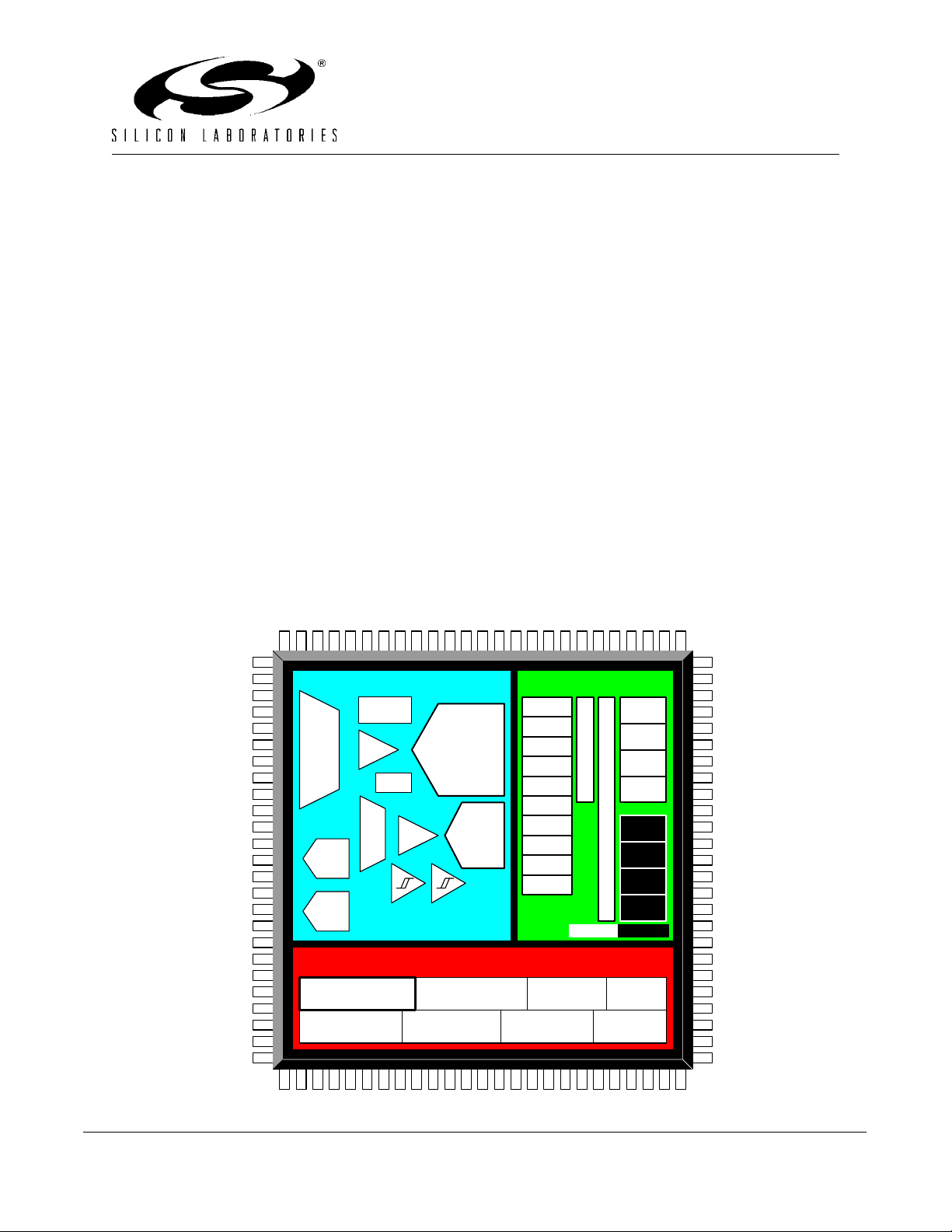
1. SYSTEM OVERVIEW
The C8051F020/1/2/3 devices are fully integrated mixed-signal System-on-a-Chip MCU s with 64 digital I/O pins
(C8051F020/2) or 32 digital I/O pins (C8051F021/3). Highlighted features are listed below; refer to
specific product feature selection.
• High-Speed pipelined 8051-compatible CIP-51 microcontroller core (up to 25 MIPS)
• In-system, full-speed, non-intrusive debug interface (on-chip)
• True 12-bit (C8051F020/1) or 10-bit (C8051F022/3) 100 ksps 8-channel ADC with PGA and analog multiplexer
• True 8-bit ADC 500 ksps 8-channel ADC with PGA and analog multiplexer
• Two 12-bit DACs with programmable update scheduling
• 64k bytes of in-system programmable FLASH memory
• 4352 (4096 + 256) bytes of on-chip RAM
• External Data Memory Interface with 64k byte address space
•SPI, SMBus/I2C, and (2) UART serial interfaces implemented in hardware
• Five general purpose 16-bit Timers
• Programmable Counter/Timer Array with five capture/compare modules
• On-chip Watchdog Timer , VDD Monitor, and T emperature Sensor
With on-chip VDD monitor, Watchdog Timer, and clock oscillator, the C8051F020/1/2/3 devices are truly stand-
alone System-on-a-Chip solutions. All analog and digital peripherals are enabled/disabled and configured by user
firmware. The FLASH memory can be reprogrammed even in-circuit, providin g non-volatile data storage, and also
allowing field upgrades of the 8051 firmware.
Table 1.1 for
On-board JTAG debug circuitry allows non-intrusive (uses no on-chip resources), full speed, in-circuit debugging
using the production MCU installed in the final application. This debug system supports inspection and modificati on
of memory and registers, setting breakpoints, watchpoints, single stepping, run and halt commands. All analog and
digital peripherals are fully functional while de bugging using JTAG.
Each MCU is specified for 2.7 V- t o - 3 . 6 V operation over the industrial temperature range (-45° C to +85° C). The
Port I/Os, /RST, and JTAG pins are tolerant for input signals up to 5
TQFP package (see block diagrams in
package (see block diagrams in Figure 1.2 and Figure 1.4).
Figure 1.1 and Figure 1.3). The C8051F021/3 are available in a 64-pin TQFP
V. The C8051F020/2 are available in a 100-pin
Tab le 1.1. Product Selection Guide
C
2
MIPS (Peak)
FLASH Memory
RAM
External Memory Interface
SMBus/I
SPI
UARTS
Tim ers (16 -b it)
Programmable Counter Array
Digital Port I/O’s
12-bit 100ksps ADC Inputs
10-bit 100ksps ADC Inputs
8-bit 500ksps ADC Inputs
Vol t a ge Refer e nce
Temperature Sensor
DAC Resolution (bits)
DAC Outputs
C8051F020 25 64k 4352
C8051F021 25 64k 4352
3 3 3
3 3 3
2 5
2 5
3
64 8 - 8
3
32 8 - 8
3 3
3 3
Analog Comparators
12 2 2 100TQFP
12 2 2 64TQFP
Package
C8051F022 25 64k 4352
C8051F023 25 64k 4352
3 3 3
3 3 3
2 5
2 5
3
64 - 8 8
3
32 - 8 8
Rev. 1.4 17
3 3
3 3
12 2 2 100TQFP
12 2 2 64TQFP
Page 18
C8051F020/1/2/3
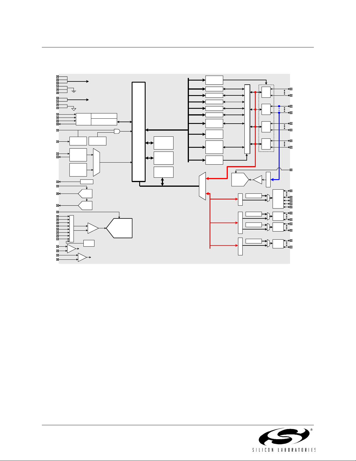
Figure 1.1. C8051F020 Block Diagram
VDD
VDD
VDD
DGND
DGND
DGND
AV+
AV+
AGND
AGND
TCK
TMS
TDI
TDO
/RST
MONEN
XTAL1
XTAL2
VREF
VREFD
DAC1
DAC0
VREF0
AIN0.0
AIN0.1
AIN0.2
AIN0.3
AIN0.4
AIN0.5
AIN0.6
AIN0.7
CP0+
CP0-
CP1+
CP1-
Digital Power
Analog Power
JTAG
Logic
VDD
Monitor
External
Oscillator
Circuit
Internal
Oscillator
A
M
U
X
CP0
CP1
VREF
DAC1
(12-Bit)
DAC0
(12-Bit)
TEMP
SENSOR
Prog
Gain
Boundary Scan
Debug HW
WDT
System
Clock
Reset
ADC
100ksps
(12-Bit)
8
0
5
1
C
o
r
e
SFR Bus
64kbyte
FLASH
256 byte
RAM
4kbyte
RAM
External Data Memory Bus
Port I/O
Config.
UART0
UART1
SMBus
SPI Bus
PCA
Timers 0,
1, 2, 4
Timer 3/
RTC
P0, P1,
P2, P3
Latches
Crossbar
Config.
Address Bus
Bus Control
Data Bus
ADC
500ksps
(8-Bit)
C
T
L
A
d
d
D
a
a
r
t
C
R
O
S
S
B
A
R
P4 Latch
P5 Latch
P6 Latch
P7 Latch
P0
Drv
P1
Drv
P2
Drv
P3
Drv
A
8:1
M
Prog
Gain
U
X
P4
DRV
P5
DRV
P6
DRV
P7
DRV
P0.0
P0.7
P1.0/AIN1.0
P1.7/AIN1.7
P2.0
P2.7
P3.0
P3.7
VREF1
P4.0
P4.4
P4.5/ALE
P4.6/RD
P4.7/WR
P5.0/A8
P5.7/A15
P6.0/A0
P6.7/A7
P7.0/D0
P7.7/D7
18 Rev. 1.4
Page 19
Figure 1.2. C8051F021 Block Diagram
C8051F020/1/2/3
VDD
VDD
VDD
DGND
DGND
DGND
AV+
AGND
TCK
TMS
TDI
TDO
/RST
MONEN
XTAL1
XTAL2
VREF
DAC1
DAC0
VREFA
AIN0.0
AIN0.1
AIN0.2
AIN0.3
AIN0.4
AIN0.5
AIN0.6
AIN0.7
CP0+
CP0-
CP1+
CP1-
Digital Power
Analog Power
VDD
Monitor
External
Oscillator
Circuit
Internal
Oscillator
A
M
U
X
CP0
JTAG
Logic
VREF
(12-Bit)
(12-Bit)
CP1
DAC1
DAC0
Boundary Scan
WDT
Prog
Gain
TEMP
SENSOR
Debug HW
System
Clock
Reset
ADC
100ksps
(12-Bit)
8
0
5
1
C
o
r
e
SFR Bus
64kbyte
FLASH
256 byte
RAM
4kbyte
RAM
External Data Memory Bus
Port I/O
Config.
UART0
UART1
SMBus
SPI Bus
PCA
Timers 0,
1, 2, 4
Timer 3/
RTC
P0, P1,
P2, P3
Latches
Crossbar
Config.
Address Bus
Bus Control
Data Bus
ADC
500ksps
(8-Bit)
C
T
L
A
d
d
r
D
a
t
a
C
R
O
S
S
B
A
R
P4 Latch
P5 Latch
P6 Latch
P7 Latch
AV+
VREFA
P0
Drv
P1
Drv
P2
Drv
P3
Drv
A
8:1
M
Prog
Gain
U
X
P4
DRV
P5
DRV
P6
DRV
P7
DRV
P0.0
P0.7
P1.0/AIN1.0
P1.7/AIN1.7
P2.0
P2.7
P3.0
P3.7
Rev. 1.4 19
Page 20
C8051F020/1/2/3
VDD
VDD
VDD
DGND
DGND
DGND
AV+
AV+
AGND
AGND
TCK
TMS
TDI
TDO
/RST
MONEN
XTAL1
XTAL2
VREF
VREFD
DAC1
DAC0
VREF0
AIN0.0
AIN0.1
AIN0.2
AIN0.3
AIN0.4
AIN0.5
AIN0.6
AIN0.7
CP0+
CP0-
CP1+
CP1-
Digital Power
Analog Power
JTAG
Logic
VDD
Monitor
External
Oscillator
Circuit
Internal
Oscillator
A
M
U
X
CP0
CP1
VREF
DAC1
(12-Bit)
DAC0
(12-Bit)
TEMP
SENSOR
Prog
Gain
Boundary Scan
Debug HW
WDT
System
Clock
Reset
ADC
100ksps
(10-Bit)
8
0
5
1
C
o
r
e
SFR Bus
64kbyte
FLASH
256 byte
RAM
4kbyte
RAM
Port I/O
Config.
UART0
UART1
SMBus
SPI Bus
PCA
Timers 0,
1, 2, 4
Timer 3/
RTC
P0, P1,
P2, P3
Latches
Crossbar
Config.
Address Bus
Bus Control
Data Bus
C
T
L
A
d
d
D
a
a
r
t
C
R
O
S
S
B
A
R
P4 Latch
P5 Latch
P6 Latch
P7 Latch
P0
Drv
P1
Drv
P2
Drv
P3
Drv
8:1
P4
DRV
P5
DRV
P6
DRV
P7
DRV
P0.0
P0.7
P1.0/AIN1.0
P1.7/AIN1.7
P2.0
P2.7
P3.0
P3.7
P4.0
P4.4
P4.5/ALE
P4.6/RD
P4.7/WR
P5.0/A8
P5.7/A15
P6.0/A0
P6.7/A7
P7.0/D0
P7.7/D7
20 Rev. 1.4
Page 21
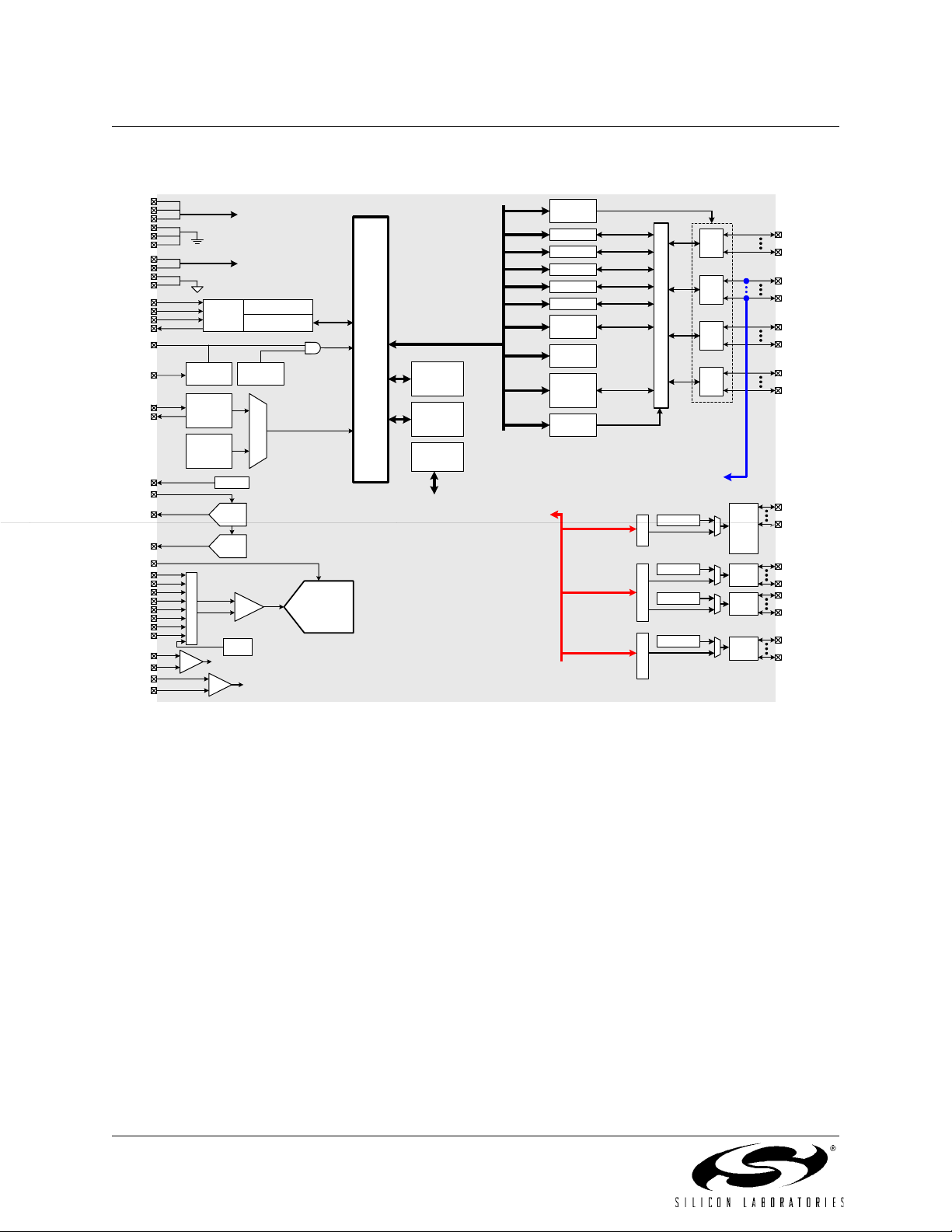
Figure 1.4. C8051F023 Block Diagram
C8051F020/1/2/3
VDD
VDD
VDD
DGND
DGND
DGND
AV+
AGND
TCK
TMS
TDI
TDO
/RST
MONEN
XTAL1
XTAL2
VREF
DAC1
DAC0
VREFA
AIN0.0
AIN0.1
AIN0.2
AIN0.3
AIN0.4
AIN0.5
AIN0.6
AIN0.7
CP0+
CP0-
CP1+
CP1-
Digital Power
Analog Power
VDD
Monitor
External
Oscillator
Circuit
Internal
Oscillator
A
M
U
X
CP0
JTAG
Logic
VREF
(12-Bit)
(12-Bit)
CP1
DAC1
DAC0
Boundary Scan
Debug HW
WDT
Prog
Gain
TEMP
SENSOR
System
Clock
Reset
ADC
100ksps
(10-Bit)
8
0
5
1
C
o
r
e
SFR Bus
64kbyte
FLASH
256 byte
RAM
4kbyte
RAM
External Data Memory Bus
Port I/O
Config.
UART0
UART1
SMBus
SPI Bus
PCA
Timers 0,
1, 2, 4
Timer 3/
RTC
P0, P1,
P2, P3
Latches
Crossbar
Config.
Bus Control
Address Bus
Data Bus
ADC
500ksps
(8-Bit)
C
T
L
A
d
d
r
D
a
t
a
C
R
O
S
S
B
A
R
P4 Latch
P5 Latch
P6 Latch
P7 Latch
AV+
VREFA
P0
Drv
P1
Drv
P2
Drv
P3
Drv
A
8:1
M
Prog
Gain
U
X
P4
DRV
P5
DRV
P6
DRV
P7
DRV
P0.0
P0.7
P1.0/AIN1.0
P1.7/AIN1.7
P2.0
P2.7
P3.0
P3.7
Rev. 1.4 21
Page 22
C8051F020/1/2/3
1.1. CIP-51™ Microcontroller Core
1.1.1. Fully 8051 Compatible
The C8051F020 family utilizes Silicon Labs' proprietary CIP-51 microcontroller core. The CIP-51 is fully compati-
ble with the MCS-51™ instruction set; standard 803x/805x assemblers and compilers can be used to develop soft-
ware. The core has all the peripherals included with a standard 8052, including five 16-bit counter/timers, two full-
duplex UARTs, 256
wide I/O Ports.
1.1.2. Improved Throughput
The CIP-51 employs a pipelined architecture that greatly increases its instruction throughput over the standard 8051
architecture. In a standard 8051, all instructions except for MUL and DIV take 12 or 24
cute with a maximum system clock of 12-to-24 MHz. By contrast, the CIP-51 core executes 70% of its instructions in
one or two system clock cycles, with only four instru ctions taking more than four system clock cycles.
The CIP-51 has a total of 109 instructions. The table below shows the total number of instructions that require each
execution time.
Clocks to Execute 1 2 2/3 3 3/4 4 4/5 5 8
bytes of internal RAM, 128 byte Special Function Register (SFR) address space, and 8/4 byte-
system clock cycles to exe-
Number of Instructions 26 50 5 14 7 3 1 2 1
With the CIP-51's maximum system clock at 25 MHz, it has a peak throughput of 25 MIPS. Figure 1.5 shows a com-
parison of peak throughputs of various 8 -bit microcontroller cores with their maximum system clocks.
Figure 1.5. Comparison of Peak MCU Execution Speeds
25
20
15
MIPS
10
5
Silicon Labs
CIP-51
(25MHz clk)
22 Rev. 1.4
Microchip
PIC17C75x
(33MHz clk)
Philips
80C51
(33MHz clk)
ADuC812
8051
(16MHz clk)
Page 23
C8051F020/1/2/3
1.1.3. Additional Features
The C8051F020 MCU family includes several key enhancements to the CIP-51 core an d peripherals to improve over-
all performance and ease of use in end applications.
The extended interrupt handler provides 22 interrupt sources into the CIP-51 (as opposed to 7 fo r th e st andard 8051),
allowing the numerous analog and digital peripherals to interrupt the controller. An interrupt driven system requires
less intervention by the MCU, giving it more effective throughput. The extra interrupt sources are very useful when
building multi-tasking, real-time systems.
There are up to seven reset sources for the MCU: an on-board VDD monitor, a Watchdog Timer, a missing clock
detector, a voltage level detection from Comparator0, a forced software reset, the CNVSTR input pin, and the /RST
pin. The /RST pin is bi-directional, accommodating an external reset, or allowing the internally generated POR to be
output on the /RST pin. Each reset source except for the VDD monitor and Reset Input pin may be disabled by the
user in software; the VDD monitor is enabled/disabled via the MONEN pin. The Watchdog Timer may be perma
nently enabled in software after a power-on reset during MCU initialization.
The MCU has an internal, stand alone clock generator which is used by default as the system clock after any reset. If
desired, the clock source may be switched on the fly to the external oscillator, which can use a crystal, ceramic reso
nator, capacitor, RC, or external clock source to generate the system clock. This can be extremely useful in low power
applications, allowing the MCU to run from a slow (power saving) external crystal source, while periodically switch
ing to the fast (up to 16 MHz) internal oscillator as needed.
-
-
-
(Port
I/O)
CP0+
CP0-
XTAL1
XTAL2
Crossbar
Internal
Clock
Generator
OSC
Figure 1.6. On-Board Clock and Reset
CNVSTR
(CNVSTR
reset
enable)
Comparator0
+
-
(CP0
reset
enable)
System
Clock
Clock Select
VDD
Missing
Clock
Detector
(one-
shot)
EN
MCD
WDT
Enable
CIP-51
Microcontroller
Core
WDT
EN
Enable
Supply
Monitor
+
-
PRE
WDT
Supply
Reset
Timeout
Strobe
Software Reset
System Reset
(wired-OR)
Reset
Funnel
/RST
Extended Interrupt
Handler
Rev. 1.4 23
Page 24
C8051F020/1/2/3
1.2. On-Chip Memory
The CIP-51 has a standard 8051 program and data address configuration . It includes 256 bytes of data RAM, with the
upper 128
addressing accesses the 128
rect addressing. The first 32 bytes are addressable as four banks of general purpose registers, and the next 16 bytes
can be byte addressable or bit addressable.
The CIP-51 in the C8051F020/1/2/3 MCUs additionally has an on-chip 4k byte RAM block and an external memory
interface (EMIF) for accessing off-chip data memory . The on-chip 4k
external data memory address range (overlapping 4k boundaries). External data memory address space can be
mapped to on-chip memory only, off-chip memory only, or a combination of the two (addresses up to 4k directed to
on-chip, above 4k directed to EMIF). The EMIF is also configurable for multiplexed or non-multipl exed address/data
lines.
The MCU’s program memory consists of 64k bytes of FLASH. This memory may be reprogrammed in-system in
512
0xFFFF are reserved for factory use. There is also a single 128
may be useful as a small table for software constants. See
bytes dual-mapped. Indirect addressing accesses the upper 128 bytes of general purpose RAM, and direct
byte SFR address space. The lower 128 bytes of RAM are accessible via direct and indi-
byte block can be addressed over the entire 64k
byte sectors, and requires no special off-chip programming voltage. The 512 bytes from addresses 0xFE00 to
byte sector at address 0x10000 to 0x1007F, which
Figure 1.7 for the MCU system memory map.
Figure 1.7. On-Chip Memory Map
PROGRAM/DATA MEMORY
(FLASH)
0x1007F
0x10000
0xFFFF
0xFE00
0xFDFF
0x0000
Scrachpad Memory
(DATA only)
RESERVED
FLASH
(In-System
Programmable in 512
Byte Sectors)
0xFF
0x80
0x7F
0x30
0x2F
0x20
0x1F
0x00
0xFFFF
DATA MEMORY (RAM)
INTERNAL DATA ADDRESS SPACE
Upper 128 RAM
(Indirect Addressing
Only)
(Direct and Indirect
Addressing)
Bit Addressable
General Purpose
Registers
Special Function
Register's
(Direct Addressing Only)
Lower 128 RAM
(Direct and Indirect
Addressing)
EXTERNAL DATA ADDRESS SPACE
Off-chip XRAM space
0x1000
0x0FFF
0x0000
24 Rev. 1.4
XRAM - 4096 Bytes
(accessable using MOVX
instruction)
Page 25
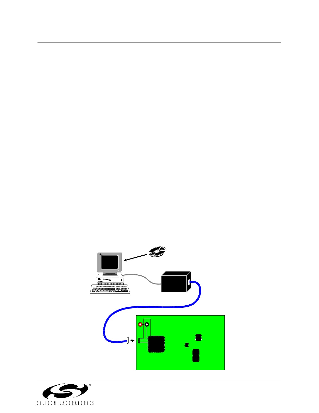
C8051F020/1/2/3
1.3. JTAG Debug and Boundary Scan
The C8051F020 family has on-chip JTAG boundary scan and debug circuitry that provides non-intrusive, full speed,
in-circuit debugging using the production part installed in the end application, via the four-pin JTAG interface. The
JTAG port is fully compliant to IEEE 1149.1, providing full boundary scan for test and manufacturing purposes.
Silicon Labs' debugging system supports inspection and m odification of memory and registers, breakpoints, watch-
points, a stack monitor, and single stepping. No additional target RAM, program memory, timers, or communicat ion s
channels are required. All the digital and analog peripherals are functional and work correctly while debugging. All
the peripherals (except for the ADC and SMBus) are stalled when the MCU is halted, during single stepping, or at a
breakpoint in order to keep them synchronized.
The C8051F020DK development kit provides all the hardware and software necessary to dev elop application code
and perform in-circuit debugging with the C8051F020/1/2/3 MCUs. The kit inclu des software with a developer's stu
dio and debugger, an integrated 8051 assembler, and an RS-232 to JTAG serial adapter . It also has a tar get application
board with the associated MCU installed, plus the RS-232 and JTAG cables, and wall-mount power supply. The
Development Kit requires a Windows 95/98/NT/ME/2000 computer with one available RS-232 serial port. As shown
in
Figure 1.8, the PC is connected via RS-232 to the Serial Adapter. A six-inch ribbon cable connects the Serial
Adapter to the user's application board, picking up the four JTAG pins and VDD and GND. The Serial Adapter takes
its power from the application board; it requires roughly 20
ficient power available from the target system, the provided power supply can be connected directly to the Serial
Adapter.
mA at 2.7-3.6 V. For applications where there is not suf-
-
Silicon Labs’ debug environment is a vastly superior con figuration for developing and debugging embedded applica-
tions compared to standard MCU emulators, which use on-board "ICE Chips" and target cables and require the MCU
in the application board to be socketed. Silicon Labs' debug environment both increases ease of use and preserves the
performance of the precision analog peripherals.
Figure 1.8. Development/In-System Debug Diagram
Silicon Labs Integrated
Development Environment
WINDOWS 95/98/NT/ME/2000
RS-232
Serial
Adapter
JTAG (x4), VDD, GND
C8051
F020
TARGET PCB
VDD GND
Rev. 1.4 25
Page 26
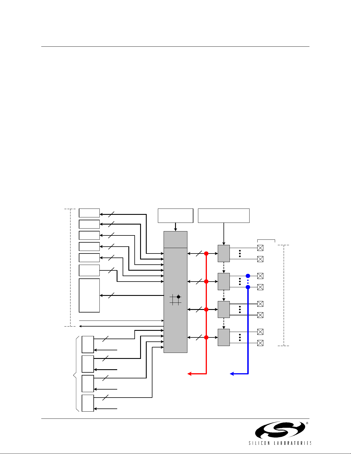
C8051F020/1/2/3
1.4. Programmable Digital I/O and Crossbar
The standard 8051 Ports (0, 1, 2, and 3) are available on the MCUs. The C8051F020/2 have 4 additional ports (4, 5,
6, and 7) for a total of 64 general-purpose port I/O. The Port I/O behave like the stand ard 8051 with a few enhance
ments.
Each Port I/O pin can be configured as either a push-pull or open-drain output. Also, the "weak pull-ups" which are
normally fixed on an 8051 can be globally disabled, providing additional power saving capabilities for low-power
applications.
Perhaps the most unique enhancement is the Digital Crossbar. This is essentially a large digital switching network
that allows mapping of internal digital system resources to Port I/O pins on P0, P1, P2, and P3. (See
Unlike microcontrollers with standard multiplexed digital I/O, all combinations of functions are supported .
The on-chip counter/timers, serial buses, HW interrupts, ADC Start of Conversion input, comparat or outputs, and
other digital signals in the controller can be configured to appear on the Port I/O pins specified in the Crossbar Con
trol registers. This allows the user to select the exact mix of general purpose Port I/O and digital resources needed for
the particular application.
Figure 1.9)
-
-
Highest
Priority
Lowest
Priority
Port
Latches
(Internal Digital Signals)
UART0
SPI
SMBus
UART1
PCA
Comptr.
Outputs
T0, T1,
T2, T2EX,
T4,T4EX
/INT0,
/INT1
/SYSCLK
CNVSTR
P0
P1
P2
P3
2
4
2
2
6
2
8
8
(P0.0-P0.7)
8
(P1.0-P1.7)
8
(P2.0-P2.7)
8
(P3.0-P3.7)
Figure 1.9. Digital Crossbar Diagram
XBR0, XBR1,
XBR2, P1MDIN
Registers
Priority
Decoder
Digital
Crossbar
To External
Memory
Interface
(EMIF)
P0MDOUT, P1MDOUT,
P2MDOUT, P3MDOUT
Registers
8
8
8
8
P0
I/O
Cells
P1
I/O
Cells
P2
I/O
Cells
P3
I/O
Cells
To
ADC1
Input
External
Pins
P0.0
P0.7
P1.0
P1.7
P2.0
P2.7
P3.0
P3.7
Highest
Priority
Lowest
Priority
26 Rev. 1.4
Page 27
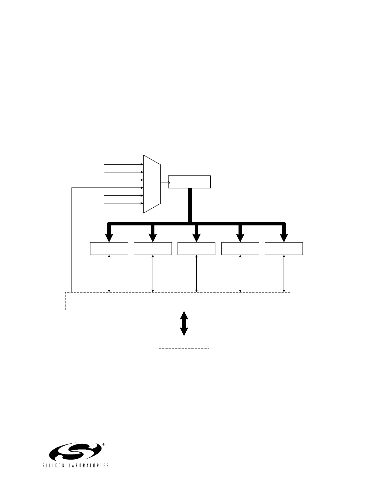
C8051F020/1/2/3
1.5. Programmable Counter Array
The C8051F020 MCU family includes an on-board Programmable Counter/Timer Array (PCA) in addition to the five
16-bit general purpose counter/timers. The PCA consists of a dedicated 16-bit counter/timer time base with 5 pro
grammable capture/compare modules. The timebase is clocked from one of six sources: the system clock divided by
12, the system clock divided by 4, Timer 0 overflow, an External Clock Input (ECI pin), the system clock, or the
external oscillator source divided by 8.
Each capture/compare module can be configured to operate in one of six modes: Edge-Triggered Capture, Software
Timer, High Speed Output, Frequency Output, 8-Bit Pulse Width Modulator, or 16-Bit Pulse Width Modulator. The
PCA Capture/Compare Module I/O and External Clock Input are routed to the MCU Port I/O via the Digital Cross
bar.
Figure 1.10. PCA Block Diagram
SYSCLK/12
SYSCLK/4
Timer 0 Overflow
ECI
SYSCLK
External Clock/8
PCA
CLOCK
MUX
16-Bit Counter/Timer
-
-
Capture/Compare
Module 1
CEX1
Capture/Compare
Module 2
CEX2
Capture/Compare
Module 3
CEX3
Capture/Compare
Module 4
CEX4
ECI
Capture/Compare
Module 0
CEX0
Crossbar
Port I/O
1.6. Serial Ports
The C8051F020 MCU Family includes two Enhanced Full-Duplex UARTs, SPI Bus, and SMBus/I2C. Each of the
serial buses is fully implemented in hardware and makes extensive use of the CIP-51's interrupts, thus requiring very
little intervention by the CPU. The serial buses do not "share" resources such as timers, interrupts, or Port I/O, so any
or all of the serial buses may be used together with any other.
Rev. 1.4 27
Page 28
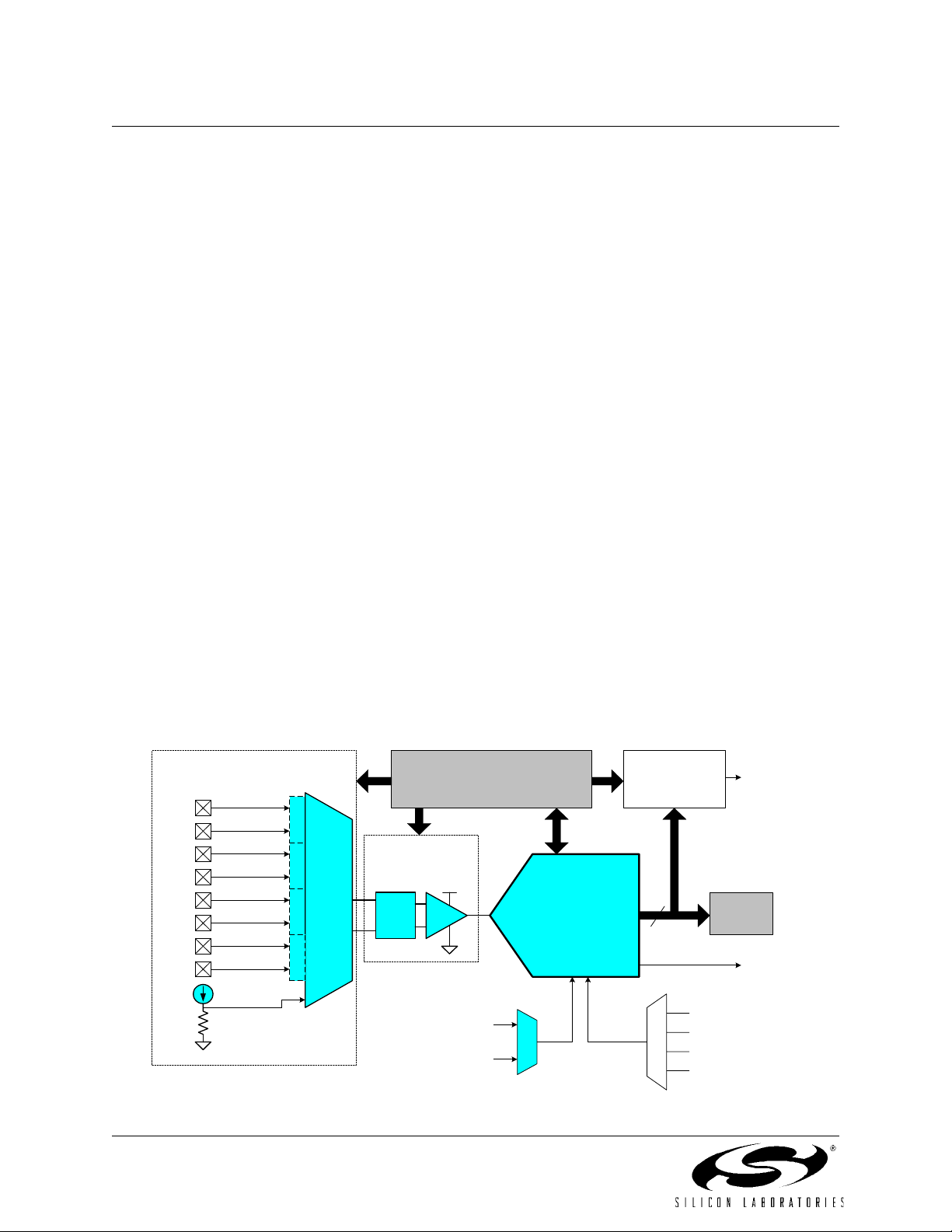
C8051F020/1/2/3
1.7. 12-Bit Analog to Digital Converter
The C8051F020/1 has an on-chip 12-bit SAR ADC (ADC0) with a 9-chann el input multiplexer and programmable
gain amplifier. W ith a maximum throughput of 100
C8051F022/3 devices include a 10-bit SAR ADC with similar specifications and configuration options. The ADC0
voltage reference is selected between the DAC0 output and an external VREF pin. O n C8051F0 20/2 devices, AD C0
has its own dedicated VREF0 input pin; on C8051F021/3 devices, the ADC0 shares the VREFA input pin with the 8-
bit ADC1. The on-chip 15
ppm/°C voltage reference may generate the voltage reference for other system components
or the on-chip ADCs via the VREF output p in.
The ADC is under full control of the CIP-51 microcontroller via its associated Special Function Registers. One input
channel is tied to an internal temperature sensor, while the other eight channels are available externally. Each pair of
the eight external input channels can be configured as either two single-ended inputs or a single differential input.
The system controller can also put the ADC into shutdown mode to save power.
A programmable gain amplifier follows the analog multiplexer. The gain can be set in software from 0.5 to 16 in
powers of 2. The gain stage can be especially useful when different ADC input channels have widely varied input
voltage signals, or when it is necessary to "zoom in" on a signal with a large DC offset (in differential mode, a DAC
could be used to provide the DC offset).
Conversions can be started in four ways; a software command, an overflow of Timer 2, an overflow of Timer 3, or an
external signal input. This flexibility allows the start of c onversion to be triggered by software events, external HW
signals, or a periodic timer overflow signal. Conversion completions are indicated by a status bit and an interrupt (i f
enabled). The resulting 10 or 12-bit data word is latched into two SFRs upon com pletion of a conversion. The data
can be right or left justified in these registers under software control.
ksps, the ADC offers true 12-bit accuracy with an INL of ±1LSB.
Window Compare registers for the ADC data can be configured to interrupt the controller when ADC data is within
or outside of a specified range. The ADC can monitor a key voltage continuously in background mode, but not inter
rupt the controller unless the converted data is within the specified window.
Figure 1.11. 12-Bit ADC Block Diagram
AIN0.0
AIN0.1
AIN0.2
AIN0.3
AIN0.4
AIN0.5
AIN0.6
AIN0.7
Analog Multiplexer
TEMP
SENSOR
AGND
+
-
+
-
+
-
+
-
9-to-1
AMUX
(SE or
DIFF)
Configuration, Control, and Data
Programmable Gain
Amplifie r
AV+
+
X
-
External VREF
DAC0 Output
Registers
Pin
12-Bit
SAR
ADC
VREF
Start
Conversion
Window Compare
Logic
12
Write to AD0BUSY
Timer 3 Overflow
CNVSTR
Timer 2 Overflow
Compare
ADC Data
Registers
Conversion
Complete
Window
Interrupt
Interrupt
-
28 Rev. 1.4
Page 29
C8051F020/1/2/3
1.8. 8-Bit Analog to Digital Converter
The C8051F020/1/2/3 has an on-board 8-bit SAR ADC (ADC1) with an 8-channel input multiplexer and program ma-
ble gain amplifier. This ADC features a 500 ksps maximum throughput and true 8-bit accuracy with an INL of
±1LSB. Eight input pins are available for measurement. The ADC is under full control of the CIP-51 microco ntroller
via the Special Function Registers. The ADC1 voltage reference is selected between the analog power supply (AV+)
and an external VREF pin. On C8051F020/2 devices, ADC1 has its o wn dedicated VREF1 input pin; on
C8051F021/3 devices, ADC1 shares the VREFA input pin with the 12/10-bit ADC0. User software may put ADC1
into shutdown mode to save power.
A programmable gain amplifier follows the analog multiplexer. The gain stage can be especially useful when differ-
ent ADC input channels have widely varied input voltage signals, or when it is necessary to "zoom in" on a signal
with a large DC offset (in differential mode, a DAC could be used to provide the DC offset). The PGA gain can be set
in software to 0.5, 1, 2, or 4.
A flexible conversion scheduling system allows ADC1 conversi ons to be initiated by software commands, timer
overflows, or an external input signal. ADC1 conversions may also be synchronized with ADC0 software-com
manded conversions. Conversion completions are indicated by a status bit and an interrupt (i f enabled), and the
resulting 8-bit data word is latched into an SFR upon completion.
Figure 1.12. 8-Bit ADC Diagram
-
AIN1.0
AIN1.1
AIN1.2
AIN1.3
AIN1.4
AIN1.5
AIN1.6
AIN1.7
Analog Multiplexer
8-to-1
AMUX
Configuration, Control, and Data Registers
Programmable Gain
Amplifier
AV+
+
X
-
External VREF
AV+
Pin
8-Bit
SAR
ADC
Start Conversion
VREF
Conversion
Complete
8
ADC Data
Register
Interrupt
Write to AD1BUSY
Timer 3 Overflow
CNVSTR Input
Timer 2 Overflow
Write to AD0BUSY
(synchronized with
ADC0)
Rev. 1.4 29
Page 30
C8051F020/1/2/3
1.9. Comparators and DACs
Each C8051F020/1/2/3 MCU has two 12-bit DACs and two comparators on chip. The MCU data and control inter-
face to each comparator and DAC is via the Special Function Registers. The MCU can place any DAC or comparator
in low power shutdown mode.
The comparators have software programmable hysteresis. Each comparator can generate an interrupt on its rising
edge, falling edge, or both; these interrupts are capable of waking up the MCU from sleep mode. The comparators'
output state can also be polled in software. The comparator outputs can be programmed to appear on the Port I/O pins
via the Crossbar.
The DACs are voltage output mode, and include a flexible output scheduling mechanism. This scheduling mecha-
nism allows DAC output updates to be forced by a software write or a Timer 2, 3, or 4 overflow. The DAC voltage
reference is supplied via the dedicated VREFD input pin on C8051F020/2 devices or via the internal voltage refer
ence on C8051F021/3 devices. The DACs are especially useful as references for the comparators or offsets for the
differential inputs of the ADC.
Figure 1.13. Comparator and DAC Diagram
-
(Port I/O)
(Port I/O)
CP0+
CP0-
CP1+
CP1-
DAC0
DAC1
CP0
CP1
+
CP0
-
+
CP1
-
REF
DAC0
REF
DAC1
CROSSBAR
CP0
CP1
SFR's
(Data
and
Cntrl)
CIP-51
and
Interrupt
Handler
30 Rev. 1.4
Page 31

2. ABSOLUTE MAXIMUM RATINGS
C8051F020/1/2/3
Tab le 2.1. Absolute Maximum Ratings
PARAMETER CONDITIONS MIN TYP MAX UNITS
Ambient temperature under bias -55 125 °C
Storage Temperature -65 150 °C
Voltage on any Pin (except VDD and Port I/O) with
respect to DGND
Voltage on any Port I/O Pin or /RST with respect to
DGND
Voltage on VDD with respect to DGND -0.3 4.2 V
Maximum Total current through VDD, AV+, DGND,
and AGND
Maximum output current sunk by any Port pin 100 mA
Maximum output current sunk by any other I/O pi n 50 mA
Maximum output current sourced by any Port pin 100 mA
Maximum output current sourced by any other I/O pin 50 mA
*
Stresses above those listed under “Absolute Maximum Ratings” may cause permanent damage to the device. This
is a stress rating only and functional operation of the devices at those or any other conditions above those indicated
in the operation listings of this specification is not implied. Exposure to maximum rating conditions for extended
periods may affect device reliability.
*
-0.3
-0.3 5.8 V
VDD +
0.3
800 mA
V
Rev. 1.4 31
Page 32

C8051F020/1/2/3
3. GLOBAL DC ELECTRICAL CHARACTERISTICS
Tab le 1.1. Global DC Electrical Characteristics
-40°C to +85°C, 25 MHz System Clock unless ot herwise specified.
PARAMETER CONDITIONS MIN TYP MAX UNITS
Analog Supply Voltag e
Analog Supply Current AV+=2.7 V, Internal REF, ADC,
DAC, Comparators all active
Analog Supply Current with
analog sub-systems inactive
Analog-to-Digital Supply Delta
(|VDD - AV+|)
Digital Supply Volt age 2.7 3.0 3.6 V
Digital Supply Current with
CPU active
Digital Supply Current with
CPU inactive (not accessing
FLASH)
Digital Supply Current (shut-
down)
Digital Supply RAM Data
Retention Voltage
AV+=2.7 V, Internal REF, ADC,
DAC, Comparators all disabled,
oscillator disabled, VDD Monitor
disabled
VDD=2.7 V, Clock=25 MHz
VDD=2.7 V, Clock=1 MHz
VDD=2.7 V, Clock=32 kHz
VDD=2.7 V, Clock=25 MHz
VDD=2.7 V, Clock=1 MHz
VDD=2.7 V, Clock=32 kHz
VDD=2.7 V, Oscillator not running,
VDD Monitor disabled
2.7
†
3.0 3.6 V
1.7 mA
0.2 µA
0.5 V
10
0.5
20
5
0.2
10
0.2 µA
1.5 V
mA
mA
µA
mA
mA
µA
Specified Operating Tempera-
ture Range
SYSCLK (system clock fre-
quency)
Tsysl (SYSCLK low time) 18 ns
Tsysh (SYSCLK high time) 18 ns
†
Analog Supply AV+ must be greater than 1 V for VDD monitor to operate.
‡
SYSCLK must be at least 32 kHz to enable debugging.
32 Rev. 1.4
-40 +85 °C
‡
0
25 MHz
Page 33

4. PINOUT AND PACKAGE DEFINITIONS
Tab le 4.1. Pin Definitions
Pin Numbers
C8051F020/1/2/3
Name
F022 F023
VDD 37, 64, 9024, 41,
57
DGND 38, 63, 8925, 40,
56
AV + 11, 14 6 Analog Supply Voltage. Must be tied to +2.7 to +3.6 V.
AGND 10, 13 5 Analog Ground. Must be tied to Ground.
TMS 1 58 D In JTAG Test Mode Select with internal pull-up.
TCK 2 59 D In JTAG Test Clock with internal pull-up.
TDI 3 60 D In JTAG Test Data Input with internal pull-up. TDI is latched on the
TDO 4 61 D Out JTAG Test Data Output with internal pull-up. Data is shifted out on
/RST 5 62 D I/O Device Reset. Open-d rain output of internal VDD monitor. Is driven
Type DescriptionF020 F021
Digital Supply Voltage. Must be tied to +2.7 to +3.6 V.
Digital Ground. Must be tied to Ground.
rising edge of TCK.
TDO on the falling edge of TCK. TDO output is a tri-state driver.
low when VDD is <2.7
can initiate a system reset by driving this pin low.
V and MONEN is high. An external source
XTAL1 26 17 A In Crystal Input. This pin is the return for the internal oscillator circuit
for a crystal or ceramic resonator. For a precision internal clock,
connect a crystal or ceramic resonator from XTAL1 to XTAL2. If
overdriven by an external CMOS clock, this becomes the system
clock.
XTAL2 27 18 A Out Crystal Output. This pin is the excitation driver for a crystal or
ceramic resonator.
MONEN 28 19 D In VDD Monitor Enable. When tied high, this pin enables the internal
VDD monitor, which forces a system reset when VDD is < 2.7
When tied low, the internal VDD monitor is disabled.
VREF 12 7 A I/O Bandgap Voltage Reference Output (all devices).
DAC Voltage Reference Input (F021/3 only).
VREFA 8 A In ADC0 and ADC1 Voltage Reference Input.
VREF0 16 A In ADC0 Voltage Reference Input.
VREF1 17 A In ADC1 Voltage Reference Input.
VREFD 15 A In DAC Voltage Reference Input.
V.
Rev. 1.4 33
Page 34

C8051F020/1/2/3
Pin Numbers
Table 4.1. Pin Definitions
Name
F022 F023
AIN0.0 18 9 A In ADC0 Input Channel 0 (See ADC0 Specification for complete
AIN0.1 19 10 A In ADC0 Input Channel 1 (See ADC0 Specificatio n for comp lete
AIN0.2 20 11 A In ADC0 Input Channel 2 (See ADC0 Specification for complete
AIN0.3 21 12 A In ADC0 Input Channel 3 (See ADC0 Specificatio n for comp lete
AIN0.4 22 13 A In ADC0 Input Channel 4 (See ADC0 Specificatio n for comp lete
AIN0.5 23 14 A In ADC0 Input Channel 5 (See ADC0 Specificatio n for comp lete
AIN0.6 24 15 A In ADC0 Input Channel 6 (See ADC0 Specificatio n for comp lete
AIN0.7 25 16 A In ADC0 Input Channel 7 (See ADC0 Specificatio n for comp lete
Type DescriptionF020 F021
description).
description).
description).
description).
description).
description).
description).
description).
CP0+ 9 4 A In Comparator 0 Non-Inverting Input.
CP0- 8 3 A In Comparator 0 Inverting Input.
CP1+ 7 2 A In Comparator 1 Non-Inverting Input.
CP1- 6 1 A In Comparator 1 Inverting Input.
DAC0 100 64 A Out Digital to Analog Converter 0 Voltage Output. (See DAC Specifica-
tion for complete description).
DAC1 99 63 A Out Digital to Analog Converter 1 Voltage Output. (See DAC Specifica-
tion for complete description).
P0.0 62 55 D I/O Port 0.0. See Port Input/O utput section for complete description.
P0.1 61 54 D I/O Port 0.1. See Port Input/O utput section for complete description.
P0.2 60 53 D I/O Port 0.2. See Port Input/O utput section for complete description.
P0.3 59 52 D I/O Port 0.3. See Port Input/O utput section for complete description.
P0.4 58 51 D I/O Port 0.4. See Port Input/O utput section for complete description.
ALE/P0.5 57 50 D I/O ALE Strobe for External Memory Address bus (multiplexed mode)
Port 0.5
See Port Input/Output section for complete description.
34 Rev. 1.4
Page 35

Pin Numbers
C8051F020/1/2/3
Table 4.1. Pin Definitions
Name
F022 F023
/RD/P0.6 56 49 D I/O /RD Strobe for External Memory Address bus
/WR/P0.7 55 48 D I/O /WR Strobe for External Memory Address bus
AIN1.0/A8/P1.0 36 29 A In
AIN1.1/A9/P1.1 35 28 A In
AIN1.2/A10/P1.2 34 27 A In
AIN1.3/A11/P1.3 33 26 A In
Type DescriptionF020 F021
D I/O
D I/O
D I/O
D I/O
Port 0.6
See Port Input/Output section for complete description.
Port 0.7
See Port Input/Output section for complete description.
ADC1 Input Channel 0 (See ADC1 Specification for complete
description).
Bit 8 External Memory Address bus (Non-multiplexed mode)
Port 1.0
See Port Input/Output section for complete description.
Port 1.1. See Port Input/Output section for complete description.
Port 1.2. See Port Input/Output section for complete description.
Port 1.3. See Port Input/Output section for complete description.
AIN1.4/A12/P1.4 32 23 A In
D I/O
AIN1.5/A13/P1.5 31 22 A In
D I/O
AIN1.6/A14/P1.6 30 21 A In
D I/O
AIN1.7/A15/P1.7 29 20 A In
D I/O
A8m/A0/P2.0 46 37 D I/O Bit 8 External Memory Address bus (Multiplexed mode)
A9m/A1/P2.1 45 36 D I/O Port 2.1. See Port Input/Output section for complete description.
A10m/A2/P2.2 44 35 D I/O Port 2.2. See Port Input/Output section for complete description .
A11m/A3/P2.3 43 34 D I/O Port 2.3. See Port Input/Output section for complete description .
A12m/A4/P2.4 42 33 D I/O Port 2.4. See Port Input/Output section for complete description .
A13m/A5/P2.5 41 32 D I/O Port 2.5. See Port Input/Output section for complete description .
Port 1.4. See Port Input/Output section for complete description.
Port 1.5. See Port Input/Output section for complete description.
Port 1.6. See Port Input/Output section for complete description.
Port 1.7. See Port Input/Output section for complete description.
Bit 0 External Memory Address bus (Non-multiplexed mode)
Port 2.0
See Port Input/Output section for complete description.
Rev. 1.4 35
Page 36

C8051F020/1/2/3
A14m/A6/P2.6 40 31 D I/O Port 2.6. See Port Input/Output section for complete description .
A15m/A7/P2.7 39 30 D I/O Port 2.7. See Port Input/Output section for complete description .
AD0/D0/P3.0 54 470 Tc(54)TjETEMC/Span <<03
D I/O
36 Rev. 1.4
Page 37

Pin Numbers
C8051F020/1/2/3
Table 4.1. Pin Definitions
Name
F022 F023
A11/P5.3 85 D I/O Port 5.3. See Port Input/Output section for complete description.
A12/P5.4 84 D I/O Port 5.4. See Port Input/Output section for complete description.
A13/P5.5 83 D I/O Port 5.5. See Port Input/Output section for complete description.
A14/P5.6 82 D I/O Port 5.6. See Port Input/Output section for complete description.
A15/P5.7 81 D I/O Port 5.7. See Port Input/Output section for complete description.
A8m/A0/P6.0 80 D I/O Bit 8 External Mem ory Address bus (Multiplexed mode)
A9m/A1/P6.1 79 D I/O Port 6.1. See Port Input/Output sect ion for complete description.
A10m/A2/P6.2 78 D I/O Port 6.2. See Port Input/Output section for complete description.
A11m/A3/P6.3 77 D I/O Port 6.3. See Port Input/Output section for complete description.
A12m/A4/P6.4 76 D I/O Port 6.4. See Port Input/Output section for complete description.
A13m/A5/P6.5 75 D I/O Port 6.5. See Port Input/Output section for complete description.
Type DescriptionF020 F021
Bit 0 External Memory Address bus (Non-multiplexed mode)
Port 6.0
See Port Input/Output section for complete description.
A14m/A6/P6.6 74 D I/O Port 6.6. See Port Input/Output section for complete description.
A15m/A7/P6.7 73 D I/O Port 6.7. See Port Input/Output section for complete description.
AD0/D0/P7.0 72 D I/O Bit 0 External Memory Address/Data bus (Multiplexed mode)
Bit 0 External Memory Data bus (Non-multiplexed mode)
Port 7.0
See Port Input/Output section for complete description.
AD1/D1/P7.1 71 D I/O Port 7.1. See Port Input/Output section for complete description.
AD2/D2/P7.2 70 D I/O Port 7.2. See Port Input/Output section for complete description.
AD3/D3/P7.3 69 D I/O Port 7.3. See Port Input/Output section for complete description.
AD4/D4/P7.4 68 D I/O Port 7.4. See Port Input/Output section for complete description.
AD5/D5/P7.5 67 D I/O Port 7.5. See Port Input/Output section for complete description.
AD6/D6/P7.6 66 D I/O Port 7.6. See Port Input/Output section for complete description.
AD7/D7/P7.7 65 D I/O Port 7.7. See Port Input/Output section for complete description.
Rev. 1.4 37
Page 38

C8051F020/1/2/3
DAC0
DAC1
P4.0
P4.1
9998979695949392919089888786858483828180797877
100
Figure 4.1. TQFP-100 Pinout Diagram
P4.2
P4.3
P4.4
ALE/P4.5
/RD/P4.6
/WR/P4.7
VDD
DGND
A8/P5.0
A9/P5.1
A10/P5.2
A11/P5.3
A12/P5.4
A13/P5.5
A14/P5.6
A15/P5.7
A8m/A0/P6.0
A9m/A1/P6.1
A10m/A2/P6.2
A11m/A3/P6.3
A12m/A4/P6.4
76
TMS
TCK
TDI
TDO
/RST
CP1-
CP1+
CP0-
CP0+
AGND
AV+
VREF
AGND
AV+
VREFD
VREF0
VREF1
AIN0.0
AIN0.1
AIN0.2
AIN0.3
AIN0.4
AIN0.5
AIN0.6
AIN0.7
1
2
3
4
5
6
7
8
9
10
11
12
13
14
15
16
17
18
19
20
21
22
23
24
25
262728293031323334353637383940
C8051F020
C8051F022
41
424344454647484950
75
A13m/A5/P6.5
74
A14m/A6/P6.6
73
A15m/A7/P6.7
72
AD0/D0/P7.0
71
AD1/D1/P7.1
70
AD2/D2/P7.2
69
AD3/D3/P7.3
68
AD4/D4/P7.4
67
AD5/D5/P7.5
66
AD6/D6/P7.6
65
AD7/D7/P7.7
64
VDD
63
DGND
62
P0.0
61
P0.1
60
P0.2
59
P0.3
58
P0.4
57
ALE/P0.5
56
/RD/P0.6
55
/WR/P0.7
54
AD0/D0/P3.0
53
AD1/D1/P3.1
52
AD2/D2/P3.2
51
AD3/D3/P3.3
VDD
XTAL1
XTAL2
MONEN
AIN1.7/A15/P1.7
AIN1.6/A14/P1.6
AIN1.5/A13/P1.5
AIN1.4/A12/P1.4
AIN1.1/A9/P1.1
AIN1.3/A11/P1.3
AIN1.2/A10/P1.2
DGND
AIN1.0/A8/P1.0
A15m/A7/P2.7
38 Rev. 1.4
AD5/D5/P3.5
A9m/A1/P2.1
A14m/A6/P2.6
A13m/A5/P2.5
A12m/A4/P2.4
A11m/A3/P2.3
A8m/A0/P2.0
A10m/A2/P2.2
AD7/D7/P3.7/IE7
AD4/D4/P3.4
AD6/D6/P3.6/IE6
Page 39

C8051F020/1/2/3
Figure 4.2. TQFP-100 Package Drawing
100
PIN 1
DESIGNATOR
D
D1
E1 E
1
A
A1
A2
b
D
D1
e
E
E1
MIN
(mm)
-
0.05
0.95
0.17
-
-
-
-
-
NOM
(mm)
-
-
1.00
0.22
16.00
14.00
0.50
16.00
14.00
MAX
(mm)
1.20
0.15
1.05
0.27
-
-
-
-
-
A2
e
A
b
A1
Rev. 1.4 39
Page 40
C8051F020/1/2/3
DAC0
DAC1
64
63
Figure 4.3. TQFP-64 Pinout Diagram
/RST
TDO
TDI
TCK
TMS
VDD
DGND
P0.0
P0.1
P0.2
P0.3
P0.4
62
61
60
59
58
57
56
55
54
53
52
51
ALE/P0.5
/RD/P0.6
50
49
CP1-
CP1+
CP0-
CP0+
AGND
AV+
VREF
VREFA
AIN0.0
AIN0.1
AIN0.2
AIN0.3
AIN0.4
AIN0.5
AIN0.6
AIN0.7
10
11
12
13
14
15
16
1
2
3
4
5
6
7
8
9
17
18
19
C8051F021
C8051F023
20
21
22
23
24
25
26
27
28
29
30
31
32
48
/WR/P0.7
47
AD0/D0/P3.0
46
AD1/D1/P3.1
45
AD2/D2/P3.2
44
AD3/D3/P3.3
43
AD4/D4/P3.4
42
AD5/D5/P3.5
41
VDD
40
DGND
39
AD6/D6/P3.6/IE6
38
AD7/D7/P3.7/IE7
37
A8m/A0/P2.0
36
A9m/A1/P2.1
35
A10m/A2/P2.2
34
A11m/A3/P2.3
33
A12m/A4/P2.4
VDD
XTAL1
XTAL2
MONEN
AIN1.7/A15/P1.7
AIN1.6/A14/P1.6
AIN1.5/A13/P1.5
AIN1.4/A12/P1.4
DGND
40 Rev. 1.4
AIN1.3/A11/P1.3
AIN1.1/A9/P1.1
AIN1.2/A10/P1.2
A15m/A7/P2.7
AIN1.0/A8/P1.0
A14m/A6/P2.6
A13m/A5/P2.5
Page 41

C8051F020/1/2/3
Figure 4.4. TQFP-64 Package Drawing
D
D1
64
PIN 1
DESIGNATOR
A2
MIN
(mm)
A
A1
0.05
E1
E
A2
b
0.95
0.17
D
D1
1
e
A
e
E
E1
b
A1
NOM
(mm)
-
0.22
-
12.00
-
10.00
-
0.50
-
12.00
-
10.00
MAX
(mm)
-
1.20
-
0.15
-
1.05
0.27
-
-
-
-
-
Rev. 1.4 41
Page 42

C8051F020/1/2/3
Notes
42 Rev. 1.4
Page 43

C8051F020/1
5. ADC0 (12-BIT ADC, C8051F020/1 ONLY)
The ADC0 subsystem for the C8051F020/1 consists of a 9-channel, configurable analog multiplexer (AMUX0), a
programmable gain amplifier (PGA0), and a 100
track-and-hold and Programmable Window Detector (see block diagram in
Conversion Modes, and Window Detector are all configurable under software control via the Special Function Regis-
ters shown in Figure 5.1. The voltage reference used by ADC0 is selected as described in Section “9. VOLTAGE
REFERENCE (C8051F020/2)” on page 91 for C8051F020/2 devices, or Section “10. VOLTAGE REFERENCE
(C8051F021/3)” on page 93 for C8051F021/3 devices. The ADC0 su bsystem (ADC0, track-and -hold and PGA0) is
enabled only when the AD0EN bit in the ADC0 Control reg ister (ADC0CN) is set to logic 1. The ADC0 subsystem is
in low power shutdown when this bit is logic 0.
Figure 5.1. 12-Bit ADC0 Functional Block Diagram
TEMP
+
-
+
-
+
-
+
-
9-to-1
AMUX
(SE or
DIFF)
X
AIN0
AIN1
AIN2
AIN3
AIN4
AIN5
AIN6
AIN7
SENSOR
AGND
ksps, 12-bit successive-approximation-register ADC with integrated
Figure 5.1). The AMUX0, PGA0, Data
ADC0LTLADC0LTHADC0GTLADC0GTH
24
AD0EN
AV+
AV+
Comb.
Logic
12
REF
SYSCLK
AD0WINT
12-Bit
+
SAR
-
AGND
ADC
AD0CM
12
Start Conversion
ADC0L ADC0H
00
AD0BUSY (W)
Timer 3 Overflow
01
10
CNVSTR
Timer 2 Overflow
11
AIN01IC
AIN23IC
AIN45IC
AIN67IC
AMX0CF
AMX0SL
AMX0AD0
AMX0AD1
AMX0AD2
AMX0AD3
AD0SC3
AD0SC4
ADC0CF
AD0SC1
AD0SC2
AD0SC0
AMP0GN1
AMP0GN2
AMP0GN0
AD0TM
AD0EN
ADC0CN
AD0CM1
AD0BUSY
AD0INT
AD0CM0
AD0LJST
AD0WINT
AD0CM
5.1. Analog Multiplexer and PGA
Eight of the AMUX channels are available for external measurements while the ninth channel is internally connected
to an on-chip temperature sensor (temperature transfer function is shown in
programmed to operate in either differential or single-ended mode. This allows the user to select the best measure-
ment technique for each input channel, and even accommodates mode changes "on-the-fly". The AMUX defaults to
all single-ended inputs upon reset. There are two registers associated with the AMUX: the Channel Selection register
AMX0SL (
Figure 5.6), and the Configuration register AMX0CF (Figure 5.7). The table in Figure 5.6 shows AMUX
functionality by channel, for each possible configuration. The PGA amplifies the AMUX output signal by an amount
determined by the states of the AMP0GN2-0 bits in the ADC0 Configuration register, ADC0CF (
PGA can be software-programmed for gains of 0.5, 2, 4, 8 or 16. Gain defaults to unity on reset.
Rev. 1.4 43
Figure 5.2). AMUX input pairs can be
Figure 5.7). The
Page 44

C8051F020/1
The T emperature Sensor transfer function is shown in Figure 5.2. The output voltage (V
) is the PGA input when
TEMP
the Temperature Sensor is selected by bits AMX0AD3-0 in register AMX0SL; this voltage will be amplified by the
PGA according to the user-programmed PGA settings.
Figure 5.2. Temperature Sensor Transfer Function
(Volts)
1.000
0.900
0.800
V
= 0.00286(TEMPC) + 0.776
0.700
0.600
0.500
0-50 50 100
TEMP
for PGA Gain = 1
(Celsius)
5.2. ADC Modes of Operation
ADC0 has a maximum conversion speed of 100 ksps. The ADC0 conversion clock is derived from the system clock
divided by the value held in the ADCSC bits of register ADC0CF.
5.2.1. Starting a Conversion
A conversion can be initiated in one of four ways, d epending on the programmed states of the ADC0 Start of Conver-
sion Mode bits (AD0CM1, AD0CM0) in ADC0CN. Conversions may be initiated by:
1. Writing a ‘1’ to the AD0BUSY bit of ADC0CN;
2. A Timer 3 overflow (i.e. timed continuous conversions);
3. A risi ng edge detected on the external ADC convert start signal, CNVSTR;
4. A Timer 2 overflow (i.e. timed continuous conversions).
The AD0BUSY bit is set to logic 1 during conversion and restored to logic 0 when conversion is complete. The fall-
ing edge of AD0BUSY triggers an interrupt (when enabled) and sets the AD0INT interrupt flag (ADC0CN.5). Con -
verted data is available in the ADC0 data word MSB and LSB registers, ADC0H, ADC0L. Converted data can be
either left or right justified in the ADC0H:ADC0L register pair (see example in
grammed state of the AD0LJST bit in the ADC0CN register.
When initiating conversions by writing a ‘1’ to A D0BUSY, the AD0INT bit should be polled to determine wh en a
conversion has completed (ADC0 interrupts may also be used). The recommended polling procedu re is shown below .
Step 1. Write a ‘0’ to AD0INT;
Step 2. Write a ‘1’ to AD0BUSY;
Step 3. Poll AD0INT for ‘1’;
Step 4. Process ADC0 data.
Figure 5.11) depending on the pro-
44 Rev. 1.4
Page 45

C8051F020/1
5.2.2. Tracking Modes
The AD0TM bit in register ADC0CN controls the ADC0 track-and-ho ld mode. In its default state, the ADC0 input is
continuously tracked when a conversion is not in progress. When the AD0TM bit i s logic 1, ADC0 operates in low -
power track-and-hold mode. In this mode, each conversion is preceded by a tracking period of 3 SAR clocks (after
the start-of-conversion signal). When the CNVSTR signal is used to initiate conversions in low-power tracking mode,
ADC0 tracks only when CNVSTR is low; conversion begins on the rising edge of CNVSTR (see
ing can also be disabled (shutdown) when the entire chip is in low power standby or sleep modes. Lo w-power track-
and-hold mode is also useful when AMUX or PGA settings are frequently changed, to ensure that settling time
requirements are met (see
Section “5.2.3. Settling Time Requirements” on page 46).
Figure 5.3. 12-Bit ADC Track and Conversion Example Timing
A. ADC Timing for External Trigger Source
(AD0STM[1:0]=10
CNVSTR
)
12345678910111213141516
SAR Clocks
Figure 5.3). Track-
ADC0TM=1
ADC0TM=0
Timer 2, Timer 3 Overflow;
Write '1' to AD0BUSY
(AD0STM[1:0]=00, 01, 11)
SAR Clocks
ADC0TM=1
SAR Clocks
ADC0TM=0
Low Power
or Convert
Track Or Convert Convert Track
Track Convert Low Power Mode
B. ADC Timing for Internal Trigger Sources
1234567891011121314151617 18 19
Low Power
or Convert
Track or
Convert
Track Convert Low Power Mode
12345678910111213141516
Convert Track
Rev. 1.4 45
Page 46

C8051F020/1
5.2.3. Settling Time Requirements
When the ADC0 input configuration is changed (i.e., a different MUX or PGA selection is made), a minimum settling
(or tracking) time is required before an accurate conversion can be performed. This settling time is determined by the
ADC0 MUX resistance, the ADC0 sampling capacitance, any external source resistance, and the accuracy required
for the conversion.
modes. Notice that the equivalent time constant for both inpu t circuits is the same. The required settling time for a
given settling accuracy (SA) may be approximated by
R
reduces to R
TOTAL
every conversion. For most applications, these three SAR clocks will meet the tracking requirements. See
on page 58 for absolute minimum settling/tracking time requirements.
Where:
SA is the settling accuracy, given as a fraction of an LSB (for example, 0.25 to settle within 1/4 LSB)
t is the required settling time in seconds
R
is the sum of the ADC0 MUX resistance and any external source resistance.
TOTAL
n is the ADC resolution in bits (12).
Figure 5.4 shows the equivalent ADC0 input circuits for both Differential and Single-ended
Equation 5.1. When measuring the Temperature Sensor output,
. Note that in low-power tracking mode, three SAR clocks are used for tracking at the start of
MUX
Table 5.1
Equation 5.1. ADC0 Settling Time Requirements
n
2
t
------ -
×ln=
SA
R
TOTALCSAMPLE
AIN0.x
AIN0.y
Figure 5.4. ADC0 Equivalent Input Circuits
Differential Mode
MUX Select
R
= 5k
MUX
RC
= R
MUX
* C
R
MUX
SAMP LE
= 5k
Input
MUX Select
C
SAMPLE
C
SAMPLE
= 10pF
= 10pF
Single-Ended Mode
MUX Select
AIN0.x
RC
Input
= R
MUX
R
* C
MUX
SAMPL E
= 5k
C
SAMPLE
= 10pF
46 Rev. 1.4
Page 47

C8051F020/1
Figure 5.5. AMX0CF: AMUX0 Configuration Register (C8051F020/1)
R/W R/W R/W R/W R/W R/W R/W R/W Reset Value
- - - - AIN67IC AIN45IC AIN23 IC AIN01IC 00000000
Bit7 Bit6 Bit5 Bit4 Bit3 Bit2 Bit1 Bit0 SFR Address:
Bits7-4: UNU SED. Read = 00 00b; Write = don’t care
Bit3: AIN67IC: AIN6, AIN7 Input Pair Configuration Bit
0: AIN6 and AIN7 are independent single-ended inputs
1: AIN6, AIN7 are (respectively) +, - differential input pair
Bit2: AIN45IC: AIN4, AIN5 Input Pair Configuration Bit
0: AIN4 and AIN5 are independent single-ended inputs
1: AIN4, AIN5 are (respectively) +, - differential input pair
Bit1: AIN23IC: AIN2, AIN3 Input Pair Configuration Bit
0: AIN2 and AIN3 are independent single-ended inputs
1: AIN2, AIN3 are (respectively) +, - differential input pair
Bit0: AIN01IC: AIN0, AIN1 Input Pair Configuration Bit
0: AIN0 and AIN1 are independent single-ended inputs
1: AIN0, AIN1 are (respectively) +, - differential input pair
0xBA
NOTE: The ADC0 Data Word is in 2’s complement format for channels configured as differential.
Rev. 1.4 47
Page 48

C8051F020/1
Figure 5.6. AMX0SL: AMUX0 Channel Select Register (C8051F020/1)
R/W R/W R/W R/W R/W R/W R/W R/W Reset Value
- - - - AMX0AD3 AM X0A D2 AMX0AD1 AMX0AD0 00000000
Bit7 Bit6 Bit5 Bit4 Bit3 Bit2 Bit1 Bit0 SFR Address:
Bits7-4: UNU SED. Read = 00 00b; Write = don’t care
Bits3-0: AMX0AD3 -0: AMX0 Address Bits
0000-1111b: ADC Inputs selected per chart below
AMX0AD3-0
0000 0001 0010 0011 0100 0101 0110 0111 1xxx
0000
0001
0010
0011
0100
0101
0110
0111
1000
1001
AMX0CF Bits 3-0
1010
1011
1100
1101
1110
1111
AIN0 AIN1 AIN2 AIN3 AIN4 AIN5 AIN6 AIN7
+(AIN0)
-(AIN1)
AIN0 AIN1
+(AIN0)
-(AIN1)
AIN0 AIN1 AIN2 AIN3
+(AIN0)
-(AIN1)
AIN0 AIN1
+(AIN0)
-(AIN1)
AIN0 AIN1 AIN2 AIN3 AIN4 AIN5
+(AIN0)
-(AIN1)
AIN0 AIN1
+(AIN0)
-(AIN1)
AIN0 AIN1 AIN2 AIN3
+(AIN0)
-(AIN1)
AIN0 AIN1
+(AIN0)
-(AIN1)
AIN2 AIN3 AIN4 AIN5 AIN6 AIN7
+(AIN2)
-(AIN3)
+(AIN2)
-(AIN3)
AIN2 AIN3
+(AIN2)
-(AIN3)
+(AIN2)
-(AIN3)
AIN2 AIN3 AIN4 AIN5
+(AIN2)
-(AIN3)
+(AIN2)
-(AIN3)
AIN2 AIN3
+(AIN2)
-(AIN3)
+(AIN2)
-(AIN3)
AIN4 AIN5 AIN6 AIN7
AIN4 AIN5 AIN6 AIN7
+(AIN4)
-(AIN5)
+(AIN4)
-(AIN5)
+(AIN4)
-(AIN5)
+(AIN4)
-(AIN5)
AIN4 AIN5
AIN4 AIN5
+(AIN4)
-(AIN5)
+(AIN4)
-(AIN5)
+(AIN4)
-(AIN5)
+(AIN4)
-(AIN5)
AIN6 AIN7
AIN6 AIN7
AIN6 AIN7
AIN6 AIN7
+(AIN6)
-(AIN7)
+(AIN6)
-(AIN7)
+(AIN6)
-(AIN7)
+(AIN6)
-(AIN7)
+(AIN6)
-(AIN7)
+(AIN6)
-(AIN7)
+(AIN6)
-(AIN7)
+(AIN6)
-(AIN7)
0xBB
TEMP
SENSOR
TEMP
SENSOR
TEMP
SENSOR
TEMP
SENSOR
TEMP
SENSOR
TEMP
SENSOR
TEMP
SENSOR
TEMP
SENSOR
TEMP
SENSOR
TEMP
SENSOR
TEMP
SENSOR
TEMP
SENSOR
TEMP
SENSOR
TEMP
SENSOR
TEMP
SENSOR
TEMP
SENSOR
48 Rev. 1.4
Page 49

C8051F020/1
A
Figure 5.7. ADC0CF: ADC0 Configuration Register (C8051F020/1)
R/W R/W R/W R/W R/W R/W R/W R/W Reset Value
AD 0SC 4 AD 0S C3 AD 0S C2 AD 0S C1 AD 0S C0 AM P0 GN 2 A MP0 GN 1 A MP0 GN 0 111110 00
Bit7 Bit6 Bit5 Bit4 Bit3 Bit2 Bit1 Bit0 SFR Address:
0xBC
Bits7-3: AD0 SC4 -0: ADC0 SAR Conv ersion Clock Period Bits
SAR Conversion clock is derived from system clock by the followi ng equation, where AD0SC refers
to the 5-bit value held in AD0SC4-0, and CLK
T able 5.1 on page 58 for SAR clock setting requirements.
D0SC
Bits2-0: AMP0GN2-0 : ADC0 Internal Amplifier Gain (PGA)
000: Gain = 1
001: Gain = 2
010: Gain = 4
011: Gain = 8
10x: Gain = 16
11x: Gain = 0.5
SYSCLK
---------------------- -1–=
CLK
SAR0
refers to the desired ADC0 SAR clock. See
SAR0
Rev. 1.4 49
Page 50

C8051F020/1
Figure 5.8. ADC0CN: ADC0 Control Register (C8051F020/1)
R/W R/W R/W R/W R/W R/W R/W R/W Reset Value
AD0EN AD0TM AD0INT AD0BUSY AD0CM1 AD0CM0 AD0WINT AD0LJST 00000000
Bit7 Bit6 Bit5 Bit4 Bit3 Bit2 Bit1 Bit0 SFR Address:
(bit addressable)
Bit7: AD0EN: ADC0 Enable Bit.
0: ADC0 Disabled. ADC0 is in low-power shutdown.
1: ADC0 Enabled. ADC0 is active and ready for data conversions.
Bit6: AD0TM: ADC Track Mode Bit
0: When the ADC is enabled, tracking is continuous unless a conversion is in process
1: Tracking Defined by ADSTM1-0 bits
Bit5: AD0INT: ADC0 Conversion Complete Interrupt Flag.
This flag must be cleared by software.
0: ADC0 has not completed a data conversion since the last time this flag was cleared.
1: ADC0 has completed a data conversion.
Bit4: AD0BUSY: ADC0 Busy Bit.
Read:
0: ADC0 Conversion is complete or a conversion is not currently in progress. AD0INT is set to
logic 1 on the falling edge of AD0BUSY.
1: ADC0 Conversion is in progress.
Write:
0: No Effect.
1: Initiates ADC0 Conversion if AD0STM1-0 = 00b
Bit3-2: AD0CM1-0: ADC0 Start of Conversion Mode Select.
If AD0TM = 0:
00: ADC0 conversion initiated on every write of ‘1’ t o AD0BUSY.
01: ADC0 conversion initiated on over flow of Timer 3.
10: ADC0 conversion initiated on rising edge of external CNVSTR.
11: ADC0 conversion initiated on overflow of Timer 2.
If AD0TM = 1:
00: Tracking starts with the write of ‘1’ to AD0BUSY and lasts for 3 SAR clocks, followed by con-
version.
01: Tracking started by the overflow of Timer 3 and last for 3 SAR clocks, followed by conversion.
10: ADC0 tracks only when CNVSTR input is logic low; conversion starts on rising CNVSTR edge.
11: Tracking started by the overflow of Timer 2 and last for 3 SAR clocks, followed by conversion.
Bit1: AD0WINT: ADC0 Window Compare Interrupt Flag.
This bit must be cleared by software.
0: ADC0 Window Comparison Data match has not occurred since this flag was last cleared.
1: ADC0 Window Comparison Data match has occurred.
Bit0: AD0LJST: ADC0 Left Justify Select.
0: Data in ADC0H:ADC0L registers are right-justified.
1: Data in ADC0H:ADC0L registers are left-justified.
0xE8
50 Rev. 1.4
Page 51

C8051F020/1
Figure 5.9. ADC0H: ADC0 Data Word MSB Register (C8051F020/1)
R/W R/W R/W R/W R/W R/W R/W R/W Reset Value
Bit7 Bit6 Bit5 Bit4 Bit3 Bit2 Bit1 Bit0 SFR Address:
Bits7-0: ADC0 Data Word High-Order Bits.
For AD0LJST = 0: Bits 7-4 are the sign extension of Bit3. Bits 3-0 are the upper 4 bits of the 12-bit
ADC0 Data Word.
For AD0LJST = 1: Bits 7-0 are the most-significant bits of the 12-bit ADC0 Data Word.
Figure 5.10. ADC0L: ADC0 Data Word LSB Register (C8051F020/1)
R/W R/W R/W R/W R/W R/W R/W R/W Reset Value
Bit7 Bit6 Bit5 Bit4 Bit3 Bit2 Bit1 Bit0 SFR Address:
00000000
0xBF
00000000
0xBE
Bits7-0: ADC0 Data Word Low-Order Bits.
For AD0LJST = 0: Bits 7-0 are the lower 8 bits of the 12-bit ADC0 Data Word.
For AD0LJST = 1: Bits 7-4 are the lower 4 bits of the 12-bit ADC0 Data Word. Bits3-0 will always
read ‘0’.
Rev. 1.4 51
Page 52

C8051F020/1
Figure 5.11. ADC0 Data Word Example (C8051F020/1)
12-bit ADC0 Data Word appears in the ADC0 Data Word Registers as follows:
ADC0H[3:0]:ADC0L[7:0], if AD0LJST = 0
(ADC0H[7:4] will be sign-extension of ADC0H.3 for a differential reading, otherwise =
0000b).
ADC0H[7:0]:ADC0L[7:4], if AD0LJST = 1
(ADC0L[3:0] = 0000b).
Example: ADC0 Data Word Conversion Map, AIN0 Input in Single-Ended Mode
(AMX0CF = 0x00, AMX0SL = 0x00)
AIN0-AGND (Volts)
VREF * (4095/4096) 0x0FFF 0xFFF0
VREF / 2 0x0800 0x8000
VREF * (2047/4096) 0x07FF 0x7FF0
0 0x0000 0x0000
ADC0H:ADC0L
(AD0LJST = 0)
ADC0H:ADC0L
(AD0LJST = 1)
Example: ADC0 Data Word Conversion Map, AIN0-AIN1 Differential Input Pair
(AMX0CF = 0x01, AMX0SL = 0x00)
AIN0-AGND (Volts)
VREF * (2047/2048) 0x07FF 0x7FF0
VREF / 2 0x0400 0x4000
VREF * (1/2048) 0x0001 0x0010
0 0x0000 0x0000
-VREF * (1/2048) 0xFFFF (-1d) 0xFFF0
-VREF / 2 0xFC00 (-1024d) 0xC000
-VREF 0xF800 (-2048d) 0x8000
For AD0LJST = 0:
Code Vin
× 2n×=
ADC0H:ADC0L
(AD0LJST = 0)
Gain
---------------
VREF
; ‘n’ = 12 for Single-Ended; ‘n’=11 for Differential.
ADC0H:ADC0L
(AD0LJST = 1)
52 Rev. 1.4
Page 53

C8051F020/1
5.3. ADC0 Programmable Window Detector
The ADC0 Programmable Window Detector continuously compares the ADC0 output to user-programmed limits,
and notifies the system when an out-of-bound condition is detected. This is especially effective in an interrupt-driven
system, saving code space and CPU bandwidth while delivering faster system response times. The window detector
interrupt flag (AD0WINT in ADC0CN) can also be used in polled mode. The high and low bytes of the reference
words are loaded into the ADC0 Greater-Than and ADC0 Less-Than registers (ADC0GTH, ADC0GTL, ADC0LTH,
and ADC0LTL). Reference comparisons are shown starting on
asserted when the measured data is inside or outside the user-programmed limits, depending on the programming of
the ADC0GTx and ADC0LTx registers.
Figure 5.12. ADC0GTH: ADC0 Greater-Than Data High Byte Register (C8051F020/1)
R/W R/W R/W R/W R/W R/W R/W R/W Reset Value
Bit7 Bit6 Bit5 Bit4 Bit3 Bit2 Bit1 Bit0 SFR Address:
Bits7-0: High byte of ADC0 Greater-Than Data Word.
page 54. Notice that the window detector flag can be
11111111
0xC5
Figure 5.13. ADC0GTL: ADC0 Greater-Than Data Low Byte Register (C8051F020/1)
R/W R/W R/W R/W R/W R/W R/W R/W Reset Value
11111111
Bit7 Bit6 Bit5 Bit4 Bit3 Bit2 Bit1 Bit0 SFR Address:
0xC4
Bits7-0: Low byte of ADC0 Greater-Than Data Word.
Figure 5.14. ADC0LTH: ADC0 Less-Than Data High Byte Register (C8051F020/1)
R/W R/W R/W R/W R/W R/W R/W R/W Reset Value
00000000
Bit7 Bit6 Bit5 Bit4 Bit3 Bit2 Bit1 Bit0 SFR Address:
0xC7
Bits7-0: High byte of ADC0 Less-Than Data Word.
Figure 5.15. ADC0LTL: ADC0 Less-Than Data Low Byte Register (C8051F020/1)
R/W R/W R/W R/W R/W R/W R/W R/W Reset Value
00000000
Bit7 Bit6 Bit5 Bit4 Bit3 Bit2 Bit1 Bit0 SFR Address:
0xC6
Bits7-0: Low byte of ADC0 Less-Than Data Word.
Rev. 1.4 53
Page 54

C8051F020/1
Figure 5.16. 12-Bit ADC0 Window Interrupt Example: Right Justified Single-Ended Data
Input Voltage
(AD0 - AGND)
REF x (4095/4096)
REF x (512/4096)
REF x (256/4096)
0
ADC Data
Word
0x0FFF
0x0201
0x0200
0x01FF
0x0101
0x0100
0x00FF
0x0000
AD0WINT
not affected
ADC0LTH:ADC0LTL
AD0WINT=1
ADC0GTH:ADC0GTL
AD0WINT
not affected
Given:
AMX0SL = 0x00, AMX0CF = 0x00
AD0LJST = ‘0’,
ADC0LTH:ADC0LTL = 0x0200,
ADC0GTH:ADC0GTL = 0x0100.
An ADC0 End of Conversion will cause an ADC0
Window Compare Interrupt (AD0WINT = ‘1’) if
the resulting ADC0 Data Word is < 0x0200 and
> 0x0100.
Input Voltage
(AD0 - AGND)
REF x (4095/4096)
REF x (512/4096)
REF x (256/4096)
0
ADC Data
Word
0x0FFF
0x0201
0x0200
0x01FF
0x0101
0x0100
0x00FF
0x0000
AD0WINT=1
ADC0GTH:ADC0GTL
AD0WINT
not affected
ADC0LTH:ADC0LTL
AD0WINT=1
Given:
AMX0SL = 0x00, AMX0CF = 0x00,
AD0LJST = ‘0’,
ADC0LTH:ADC0LTL = 0x0100,
ADC0GTH:ADC0GTL = 0x0200.
An ADC0 End of Conversion will cause an ADC0
Window Compare Interrupt (AD0WINT = ‘1’) if
the resulting ADC0 Data Word is > 0x0200 or
< 0x0100.
54 Rev. 1.4
Page 55

C8051F020/1
Figure 5.17. 12-Bit ADC0 Window Interrupt Example: Right Justified Differential Data
Input Voltage
(AD0 - AD1)
REF x (2047/2048)
REF x (256/2048)
REF x (-1/2048)
-REF
ADC Data
Word
0x07FF
0x0101
0x0100
0x00FF
0x0000
0xFFFF
0xFFFE
0xF800
AD0WINT
not affected
ADC0LTH:ADC0LTL
AD0WINT=1
ADC0GTH:ADC0GTL
AD0WINT
not affected
Given:
AMX0SL = 0x00, AMX0CF = 0x01,
AD0LJST = ‘0’,
ADC0LTH:ADC0LTL = 0x0100,
ADC0GTH:ADC0GTL = 0xFFFF.
An ADC0 End of Conversion will cause an ADC0
Window Compare Interrupt (AD0WINT = ‘1’) if
the resulting ADC0 Data Word is < 0x0100 and
> 0xFFFF. (In two’s-complement math,
0xFFFF = -1.)
Input Voltage
(AD0 - AD1)
REF x (2047/2048)
REF x (256/2048)
REF x (-1/2048)
-REF
ADC Data
Word
0x07FF
0x0101
0x0100
0x00FF
0x0000
0xFFFF
0xFFFE
0xF800
AD0WINT=1
ADC0GTH:ADC0GTL
AD0WINT
not affected
ADC0LTH:ADC0LTL
AD0WINT=1
Given:
AMX0SL = 0x00, AMX0CF = 0x01,
AD0LJST = ‘0’,
ADC0LTH:ADC0LTL = 0xFFFF,
ADC0GTH:ADC0GTL = 0x0100.
An ADC0 End of Conversion will cause an ADC0
Window Compare Interrupt (AD0WINT = ‘1’) if
the resulting ADC0 Data Word is < 0xFFFF or
> 0x0100. (In two’s-complement math,
0xFFFF = -1.)
Rev. 1.4 55
Page 56

C8051F020/1
Figure 5.18. 12-Bit ADC0 Window Interrupt Example: Left Justified Single-Ended Data
Input Voltage
(AD0 - AGND)
REF x (4095/4096)
REF x (512/4096)
REF x (256/4096)
0
ADC Data
Word
0xFFF0
0x2010
0x2000
0x1FF0
0x1010
0x1000
0x0FF0
0x0000
AD0WINT
not affected
ADC0LTH:ADC0LTL
AD0WINT=1
ADC0GTH:ADC0GTL
AD0WINT
not affected
Given:
AMX0SL = 0x00, AMX0CF = 0x00,
AD0LJST = ‘1’,
ADC0LTH:ADC0LTL = 0x2000,
ADC0GTH:ADC0GTL = 0x1000.
An ADC0 End of Conversion will cause an ADC0
Window Compare Interrupt (AD0WINT = ‘1’) if
the resulting ADC0 Data Word is < 0x2000 and
> 0x1000.
Input Voltage
(AD0 - AGND)
REF x (4095/4096)
REF x (512/4096)
REF x (256/4096)
0
ADC Data
Word
0xFFF0
0x2010
0x2000
0x1FF0
0x1010
0x1000
0x0FF0
0x0000
AD0WINT=1
ADC0GTH:ADC0GTL
AD0WINT
not affected
ADC0LTH:ADC0LTL
AD0WINT=1
Given:
AMX0SL = 0x00, AMX0CF = 0x00,
AD0LJST = ‘1’
ADC0LTH:ADC0LTL = 0x1000,
ADC0GTH:ADC0GTL = 0x2000.
An ADC0 End of Conversion will cause an ADC0
Window Compare Interrupt (AD0WINT = ‘1’) if
the resulting ADC0 Data Word is < 0x1000 or
> 0x2000.
56 Rev. 1.4
Page 57

C8051F020/1
Figure 5.19. 12-Bit ADC0 Window Interrupt Example: Left Justified Differential Data
Input Voltage
(AD0 - AD1)
REF x (2047/2048)
REF x (256/2048)
REF x (-1/2048)
-REF
ADC Data
Word
0x7FF0
0x1010
0x1000
0x0FF0
0x0000
0xFFF0
0xFFE0
0x8000
AD0WINT
not affected
ADC0LTH:ADC0LTL
AD0WINT=1
ADC0GTH:ADC0GTL
AD0WINT
not affected
Given:
AMX0SL = 0x00, AMX0CF = 0x01,
AD0LJST = ‘1’,
ADC0LTH:ADC0LTL = 0x1000,
ADC0GTH:ADC0GTL = 0xFFF0.
An ADC0 End of Conversion will cause an ADC0
Window Compare Interrupt (AD0WINT = ‘1’) if
the resulting ADC0 Data Word is < 0x1000 and
> 0xFFF0. (Two’s-complement math.)
Input Voltage
(AD0 - AD1)
REF x (2047/2048)
REF x (256/2048)
REF x (-1/2048)
-REF
ADC Data
Word
0x7FF0
0x1010
0x1000
0x0FF0
0x0000
0xFFF0
0xFFE0
0x8000
AD0WINT=1
ADC0GTH:ADC0GTL
AD0WINT
not affected
ADC0LTH:ADC0LTL
AD0WINT=1
Given:
AMX0SL = 0x00, AMX0CF = 0x01,
AD0LJST = ‘1’,
ADC0LTH:ADC0LTL = 0xFFF0,
ADC0GTH:ADC0GTL = 0x1000.
An ADC0 End of Conversion will cause an ADC0
Window Compare Interrupt (AD0WINT = ‘1’) if
the resulting ADC0 Data Word is < 0xFFF0 or
> 0x1000. (Two’s-co mpl emen t math.)
Rev. 1.4 57
Page 58

C8051F020/1
Tab le 5.1. 12-Bit ADC0 Electrical Characteristics (C8051F020/1)
VDD = 3.0V, AV+ = 3.0V, VREF = 2.40V (REFBE=0), PGA Gain = 1, -40°C to +85°C unless otherwise specified
PARAMETER CONDITIONS MIN TY P MAX UNITS
DC ACCURACY
Resolution 12 bits
Integral Nonlinearity ±1 LSB
Differential Nonlinearity Guaranteed Monotonic ±1 LSB
Offset Error -3±1 LSB
Full Scale Error Differential mode -7±3 LSB
Offset Temperature Coefficient ±0.25 ppm/°C
DYNAMIC PERFORMANCE (10 kHz sine-wave input, 0 to 1 dB below Full Scale, 100 ksps
Signal-to-Noise Plus Distortion 66 dB
Total Harmonic Distortion
Spurious-Free Dynamic Range 80 dB
CONVERSION RATE
SAR Clock Frequency 2.5 MHz
Conversion Time in SAR Clocks 16 clocks
Track/Hold Acquisition Time 1.5 µs
Throughput Rate 100 ksps
ANALOG INPUTS
Input Voltage Rang e Single-ended operation 0 VREF V
*Common-mode Voltage Range Differential operation AGND AV + V
Input Capacitance 10 pF
TEMPERATURE SENSOR
Nonlinearity -1.0 +1.0 °C
Absolute Accuracy ±3 °C
Gain PGA Gain = 1 2.86 mV/°C
Offset PGA Gain = 1, Temp = 0°C 0.776 V
POWER SPECIFICATIONS
Power Supply Current (AV+ sup-
plied to ADC)
Power Supply Rejection ±0.3 mV/V
Up to the 5th harmonic
Operating Mode, 100 ksps 450 900 µA
-75 dB
58 Rev. 1.4
Page 59

C8051F022/3
6. ADC0 (10-BIT ADC, C8051F022/3 ONLY)
The ADC0 subsystem for the C8051F022/3 consists of a 9-channel, configurable analog multiplexer (AMUX0), a
programmable gain amplifier (PGA0), and a 100
track-and-hold and Programmable Window Detector (see block diagram in
Conversion Modes, and Window Detector are all configurable under software control via the Special Function Regis-
ters shown in Figure 6.1. The voltage reference used by ADC0 is selected as described in Section “9. VOLTAGE
REFERENCE (C8051F020/2)” on page 91 for C8051F020/2 devices, or Section “10. VOLTAGE REFERENCE
(C8051F021/3)” on page 93 for C8051F021/3 devices. The ADC0 su bsystem (ADC0, track-and -hold and PGA0) is
enabled only when the AD0EN bit in the ADC0 Control reg ister (ADC0CN) is set to logic 1. The ADC0 subsystem is
in low power shutdown when this bit is logic 0.
Figure 6.1. 10-Bit ADC0 Functional Block Diagram
TEMP
+
-
+
-
+
-
+
-
9-to-1
AMUX
(SE or
DIFF)
X
AIN0
AIN1
AIN2
AIN3
AIN4
AIN5
AIN6
AIN7
SENSOR
AGND
ksps, 10-bit successive-approximation-register ADC with integrated
Figure 6.1). The AMUX0, PGA0, Data
ADC0LTLADC0LTHADC0GTLADC0GTH
20
AD0EN
AV+
AV+
Comb.
Logic
10
REF
SYSCLK
AD0WINT
10-Bit
+
SAR
-
AGND
ADC
AD0CM
10
Start Conversion
ADC0L ADC0H
00
AD0BUSY (W)
Timer 3 Overflow
01
10
CNVSTR
Timer 2 Overflow
11
AIN01IC
AIN23IC
AIN45IC
AIN67IC
AMX0CF
AMX0SL
AMX0AD0
AMX0AD1
AMX0AD2
AMX0AD3
AD0SC3
AD0SC4
ADC0CF
AD0SC1
AD0SC2
AD0SC0
AMP0GN1
AMP0GN2
AMP0GN0
AD0TM
AD0EN
ADC0CN
AD0CM1
AD0BUSY
AD0INT
AD0CM0
AD0LJST
AD0WINT
AD0CM
6.1. Analog Multiplexer and PGA
Eight of the AMUX channels are available for external measurements while the ninth channel is internally connected
to an on-chip temperature sensor (temperature transfer function is shown in
programmed to operate in either differential or single-ended mode. This allows the user to select the best measure-
ment technique for each input channel, and even accommodates mode changes "on-the-fly". The AMUX defaults to
all single-ended inputs upon reset. There are two registers associated with the AMUX: the Channel Selection register
AMX0SL (
Figure 6.6), and the Configuration register AMX0CF (Figure 6.7). The table in Figure 6.6 shows AMUX
functionality by channel, for each possible configuration. The PGA amplifies the AMUX output signal by an amount
determined by the states of the AMP0GN2-0 bits in the ADC0 Configuration register, ADC0CF (
PGA can be software-programmed for gains of 0.5, 2, 4, 8 or 16. Gain defaults to unity on reset.
Rev. 1.4 59
Figure 6.2). AMUX input pairs can be
Figure 6.7). The
Page 60

C8051F022/3
The T emperature Sensor transfer function is shown in Figure 6.2. The output voltage (V
) is the PGA input when
TEMP
the Temperature Sensor is selected by bits AMX0AD3-0 in register AMX0SL; this voltage will be amplified by the
PGA according to the user-programmed PGA settings.
Figure 6.2. Temperature Sensor Transfer Function
(Volts)
1.000
0.900
0.800
V
= 0.00286(TEMPC) + 0.776
0.700
0.600
0.500
0-50 50 100
TEMP
for PGA Gain = 1
(Celsius)
6.2. ADC Modes of Operation
ADC0 has a maximum conversion speed of 100 ksps. The ADC0 conversion clock is derived from the system clock
divided by the value held in the ADCSC bits of register ADC0CF.
6.2.1. Starting a Conversion
A conversion can be initiated in one of four ways, d epending on the programmed states of the ADC0 Start of Conver-
sion Mode bits (AD0CM1, AD0CM0) in ADC0CN. Conversions may be initiated by:
1. Writing a ‘1’ to the AD0BUSY bit of ADC0CN;
2. A Timer 3 overflow (i.e. timed continuous conversions);
3. A risi ng edge detected on the external ADC convert start signal, CNVSTR;
4. A Timer 2 overflow (i.e. timed continuous conversions).
The AD0BUSY bit is set to logic 1 during conversion and restored to logic 0 when conversion is complete. The fall-
ing edge of AD0BUSY triggers an interrupt (when enabled) and sets the AD0INT interrupt flag (ADC0CN.5). Con -
verted data is available in the ADC0 data word MSB and LSB registers, ADC0H, ADC0L. Converted data can be
either left or right justified in the ADC0H:ADC0L register pair (see example in
grammed state of the AD0LJST bit in the ADC0CN register.
When initiating conversions by writing a ‘1’ to A D0BUSY, the AD0INT bit should be polled to determine wh en a
conversion has completed (ADC0 interrupts may also be used). The recommended polling procedu re is shown below .
Step 1. Write a ‘0’ to AD0INT;
Step 2. Write a ‘1’ to AD0BUSY;
Step 3. Poll AD0INT for ‘1’;
Step 4. Process ADC0 data.
Figure 6.11) depending on the pro-
60 Rev. 1.4
Page 61

C8051F022/3
6.2.2. Tracking Modes
The AD0TM bit in register ADC0CN controls the ADC0 track-and-ho ld mode. In its default state, the ADC0 input is
continuously tracked when a conversion is not in progress. When the AD0TM bit i s logic 1, ADC0 operates in low -
power track-and-hold mode. In this mode, each conversion is preceded by a tracking period of 3 SAR clocks (after
the start-of-conversion signal). When the CNVSTR signal is used to initiate conversions in low-power tracking mode,
ADC0 tracks only when CNVSTR is low; conversion begins on the rising edge of CNVSTR (see
ing can also be disabled (shutdown) when the entire chip is in low power standby or sleep modes. Lo w-power track-
and-hold mode is also useful when AMUX or PGA settings are frequently changed, to ensure that settling time
requirements are met (see
Section “6.2.3. Settling Time Requirements” on page 62).
Figure 6.3. 10-Bit ADC Track and Conversion Example Timing
A. ADC Timing for External Trigger Source
(AD0STM[1:0]=10
CNVSTR
)
12345678910111213141516
SAR Clocks
Figure 6.3). Track-
ADC0TM=1
ADC0TM=0
Timer 2, Timer 3 Overflow;
Write '1' to AD0BUSY
(AD0STM[1:0]=00, 01, 11)
SAR Clocks
ADC0TM=1
SAR Clocks
ADC0TM=0
Low Power
or Convert
Track Or Convert Convert Track
Track Convert Low Power Mode
B. ADC Timing for Internal Trigger Sources
1234567891011121314151617 18 19
Low Power
or Convert
Track or
Convert
Track Convert Low Power Mode
12345678910111213141516
Convert Track
Rev. 1.4 61
Page 62

C8051F022/3
6.2.3. Settling Time Requirements
When the ADC0 input configuration is changed (i.e., a different MUX or PGA selection is made), a minimum settling
(or tracking) time is required before an accurate conversion can be performed. This settling time is determined by the
ADC0 MUX resistance, the ADC0 sampling capacitance, any external source resistance, and the accuracy required
for the conversion.
modes. Notice that the equivalent time constant for both inpu t circuits is the same. The required settling time for a
given settling accuracy (SA) may be approximated by
R
reduces to R
TOTAL
every conversion. For most applications, these three SAR clocks will meet the settling time requirements. See
Table 6.1 on page 74 for minimum settling/tracking time requirements.
Where:
SA is the settling accuracy, given as a fraction of an LSB (for example, 0.25 to settle within 1/4 LSB)
t is the required settling time in seconds
R
is the sum of the ADC0 MUX resistance and any external source resistance.
TOTAL
n is the ADC resolution in bits (10).
Figure 6.4 shows the equivalent ADC0 input circuits for both Differential and Single-ended
Equation 6.1. When measuring the Temperature Sensor output,
. Note that in low-power tracking mode, three SAR clocks are used for tracking at the start of
MUX
Equation 6.1. ADC0 Settling Time Requirements
n
2
t
------ -
×ln=
SA
R
TOTALCSAMPLE
AIN0.x
AIN0.y
Figure 6.4. ADC0 Equivalent Input Circuits
Differential Mode
MUX Select
R
= 5k
MUX
RC
= R
MUX
* C
R
MUX
SAMP LE
= 5k
Input
MUX Select
C
SAMPLE
C
SAMPLE
= 10pF
= 10pF
Single-Ended Mode
MUX Select
AIN0.x
RC
Input
= R
MUX
R
* C
MUX
SAMPL E
= 5k
C
SAMPLE
= 10pF
62 Rev. 1.4
Page 63

C8051F022/3
Figure 6.5. AMX0CF: AMUX0 Configuration Register (C8051F022/3)
R/W R/W R/W R/W R/W R/W R/W R/W Reset Value
- - - - AIN67IC AIN45IC AIN23 IC AIN01IC 00000000
Bit7 Bit6 Bit5 Bit4 Bit3 Bit2 Bit1 Bit0 SFR Address:
Bits7-4: UNU SED. Read = 00 00b; Write = don’t care
Bit3: AIN67IC: AIN6, AIN7 Input Pair Configuration Bit
0: AIN6 and AIN7 are independent single-ended inputs
1: AIN6, AIN7 are (respectively) +, - differential input pair
Bit2: AIN45IC: AIN4, AIN5 Input Pair Configuration Bit
0: AIN4 and AIN5 are independent single-ended inputs
1: AIN4, AIN5 are (respectively) +, - differential input pair
Bit1: AIN23IC: AIN2, AIN3 Input Pair Configuration Bit
0: AIN2 and AIN3 are independent single-ended inputs
1: AIN2, AIN3 are (respectively) +, - differential input pair
Bit0: AIN01IC: AIN0, AIN1 Input Pair Configuration Bit
0: AIN0 and AIN1 are independent single-ended inputs
1: AIN0, AIN1 are (respectively) +, - differential input pair
0xBA
NOTE: The ADC0 Data Word is in 2’s complement format for channels configured as differential.
Rev. 1.4 63
Page 64

C8051F022/3
Figure 6.6. AMX0SL: AMUX0 Channel Select Register (C8051F022/3)
R/W R/W R/W R/W R/W R/W R/W R/W Reset Value
- - - - AMX0AD3 AM X0A D2 AMX0AD1 AMX0AD0 00000000
Bit7 Bit6 Bit5 Bit4 Bit3 Bit2 Bit1 Bit0 SFR Address:
Bits7-4: UNU SED. Read = 00 00b; Write = don’t care
Bits3-0: AMX0AD3 -0: AMX0 Address Bits
0000-1111b: ADC Inputs selected per chart below
AMX0AD3-0
0000 0001 0010 0011 0100 0101 0110 0111 1xxx
0000
0001
0010
0011
0100
0101
0110
0111
1000
1001
AMX0CF Bits 3-0
1010
1011
1100
1101
1110
1111
AIN0 AIN1 AIN2 AIN3 AIN4 AIN5 AIN6 AIN7
+(AIN0)
-(AIN1)
AIN0 AIN1
+(AIN0)
-(AIN1)
AIN0 AIN1 AIN2 AIN3
+(AIN0)
-(AIN1)
AIN0 AIN1
+(AIN0)
-(AIN1)
AIN0 AIN1 AIN2 AIN3 AIN4 AIN5
+(AIN0)
-(AIN1)
AIN0 AIN1
+(AIN0)
-(AIN1)
AIN0 AIN1 AIN2 AIN3
+(AIN0)
-(AIN1)
AIN0 AIN1
+(AIN0)
-(AIN1)
AIN2 AIN3 AIN4 AIN5 AIN6 AIN7
+(AIN2)
-(AIN3)
+(AIN2)
-(AIN3)
AIN2 AIN3
+(AIN2)
-(AIN3)
+(AIN2)
-(AIN3)
AIN2 AIN3 AIN4 AIN5
+(AIN2)
-(AIN3)
+(AIN2)
-(AIN3)
AIN2 AIN3
+(AIN2)
-(AIN3)
+(AIN2)
-(AIN3)
AIN4 AIN5 AIN6 AIN7
AIN4 AIN5 AIN6 AIN7
+(AIN4)
-(AIN5)
+(AIN4)
-(AIN5)
+(AIN4)
-(AIN5)
+(AIN4)
-(AIN5)
AIN4 AIN5
AIN4 AIN5
+(AIN4)
-(AIN5)
+(AIN4)
-(AIN5)
+(AIN4)
-(AIN5)
+(AIN4)
-(AIN5)
AIN6 AIN7
AIN6 AIN7
AIN6 AIN7
AIN6 AIN7
+(AIN6)
-(AIN7)
+(AIN6)
-(AIN7)
+(AIN6)
-(AIN7)
+(AIN6)
-(AIN7)
+(AIN6)
-(AIN7)
+(AIN6)
-(AIN7)
+(AIN6)
-(AIN7)
+(AIN6)
-(AIN7)
0xBB
TEMP
SENSOR
TEMP
SENSOR
TEMP
SENSOR
TEMP
SENSOR
TEMP
SENSOR
TEMP
SENSOR
TEMP
SENSOR
TEMP
SENSOR
TEMP
SENSOR
TEMP
SENSOR
TEMP
SENSOR
TEMP
SENSOR
TEMP
SENSOR
TEMP
SENSOR
TEMP
SENSOR
TEMP
SENSOR
64 Rev. 1.4
Page 65

Figure 6.7. ADC0CF: ADC0 Configuration Register (C8051F022/3)
Bits7-3: AD0 SC4 -0: ADC0 SAR Conv ersion Clock Period Bits
SAR Conversion clock is derived from system clock by the followi ng equation, where AD0SC refers
to the 5-bit value held in AD0SC4-0, and CLK
T able 6.1 on page 74 for SAR clock setting requirements.
refers to the desired ADC0 SAR clock. See
SAR0
C8051F022/3
Rev. 1.4 65
Page 66

C8051F022/3
Figure 6.8. ADC0CN: ADC0 Control Register (C8051F022/3)
R/W R/W R/W R/W R/W R/W R/W R/W Reset Value
AD0EN AD0TM AD0INT AD0BUSY AD0CM1 AD0CM0 AD0WINT AD0LJST 00000000
Bit7 Bit6 Bit5 Bit4 Bit3 Bit2 Bit1 Bit0 SFR Address:
(bit addressable)
Bit7: AD0EN: ADC0 Enable Bit.
0: ADC0 Disabled. ADC0 is in low-power shutdown.
1: ADC0 Enabled. ADC0 is active and ready for data conversions.
Bit6: AD0TM: ADC Track Mode Bit
0: When the ADC is enabled, tracking is continuous unless a conversion is in process
1: Tracking Defined by ADSTM1-0 bits
Bit5: AD0INT: ADC0 Conversion Complete Interrupt Flag.
This flag must be cleared by software.
0: ADC0 has not completed a data conversion since the last time this flag was cleared.
1: ADC0 has completed a data conversion.
Bit4: AD0BUSY: ADC0 Busy Bit.
Read:
0: ADC0 Conversion is complete or a conversion is not currently in progress. AD0INT is set to
logic 1 on the falling edge of AD0BUSY.
1: ADC0 Conversion is in progress.
Write:
0: No Effect.
1: Initiates ADC0 Conversion if AD0STM1-0 = 00b
Bit3-2: AD0CM1-0: ADC0 Start of Conversion Mode Select.
If AD0TM = 0:
00: ADC0 conversion initiated on every write of ‘1’ t o AD0BUSY.
01: ADC0 conversion initiated on over flow of Timer 3.
10: ADC0 conversion initiated on rising edge of external CNVSTR.
11: ADC0 conversion initiated on overflow of Timer 2.
If AD0TM = 1:
00: Tracking starts with the write of ‘1’ to AD0BUSY and lasts for 3 SAR clocks, followed by con-
version.
01: Tracking started by the overflow of Timer 3 and last for 3 SAR clocks, followed by conversion.
10: ADC0 tracks only when CNVSTR input is logic low; conversion starts on rising CNVSTR edge.
11: Tracking started by the overflow of Timer 2 and last for 3 SAR clocks, followed by conversion.
Bit1: AD0WINT: ADC0 Window Compare Interrupt Flag.
This bit must be cleared by software.
0: ADC0 Window Comparison Data match has not occurred since this flag was last cleared.
1: ADC0 Window Comparison Data match has occurred.
Bit0: AD0LJST: ADC0 Left Justify Select.
0: Data in ADC0H:ADC0L registers are right-justified.
1: Data in ADC0H:ADC0L registers are left-justified.
0xE8
66 Rev. 1.4
Page 67

C8051F022/3
Figure 6.9. ADC0H: ADC0 Data Word MSB Register (C8051F022/3)
R/W R/W R/W R/W R/W R/W R/W R/W Reset Value
Bit7 Bit6 Bit5 Bit4 Bit3 Bit2 Bit1 Bit0 SFR Address:
Bits7-0: ADC Data Word High-Order Bits.
For ADLJST = 0: Bits 7-2 are the sign extension of Bit1. Bits 1-0 are the upper 2 bits of the 10-bit
ADC Data Word.
For ADLJST = 1: Bits 7-0 are the most-significant bits of the 10-bit ADC Data Word.
Figure 6.10. ADC0L: ADC0 Data Word LSB Register (C8051F022/3)
R/W R/W R/W R/W R/W R/W R/W R/W Reset Value
Bit7 Bit6 Bit5 Bit4 Bit3 Bit2 Bit1 Bit0 SFR Address:
00000000
0xBF
00000000
0xBE
Bits7-0: ADC Data Word Low-Order Bits.
For ADLJST = 0: Bits 7-0 are the lower 8 bits of the 10-bit ADC Data Word.
For ADLJST = 1: Bits 7-6 are the lower 2 bits of the 10-bit ADC Data Word. Bits 5-0 will always
read ‘0’.
Rev. 1.4 67
Page 68

C8051F022/3
Figure 6.11. ADC0 Data Word Example (C8051F022/3)
10-bit ADC Data Word appears in the ADC Data Word Registers as follows:
ADC0H[1:0]:ADC0L[7:0], if ADLJST = 0
(ADC0H[7:2] will be sign-extension of ADC0H.1 for a differential reading, otherwise =
000000b).
ADC0H[7:0]:ADC0L[7:6], if ADLJST = 1
(ADC0L[5:0] = 000000b).
Example: ADC Data Word Conversion Map, AIN0 Input in Single-Ended Mode
(AMX0CF = 0x00, AMX0SL = 0x00)
AIN0-AGND (Volts)
VREF * (1023/1024) 0x03FF 0xFFC0
VREF / 2 0x0200 0x8000
VREF * (511/1024) 0x01FF 0x7FC0
0 0x0000 0x0000
ADC0H:ADC0L
(ADLJST = 0)
ADC0H:ADC0L
(ADLJST = 1)
Example: ADC Data Word Conversion Map, AIN0-AIN1 Differential Input Pair
(AMX0CF = 0x01, AMX0SL = 0x00)
AIN0-AGND (Volts)
VREF * (511/512) 0x01FF 0x7FC0
VREF / 2 0x0100 0x4000
VREF * (1/512) 0x0001 0x0040
0 0x0000 0x0000
-VREF * (1/512) 0xFFFF (-1) 0xFFC0
-VREF / 2 0xFF00 (-256) 0xC000
-VREF 0xFE00 (-512) 0x8000
ADLJST = 0:
Code Vin
× 2n×=
ADC0H:ADC0L
(ADLJST = 0)
Gain
---------------
VREF
; ‘n’ = 10 for Single-Ended; ‘n’=9 for Differential.
ADC0H:ADC0L
(ADLJST = 1)
68 Rev. 1.4
Page 69

C8051F022/3
6.3. ADC0 Programmable Window Detector
The ADC0 Programmable Window Detector continuously compares the ADC0 output to user-programmed limits,
and notifies the system when an out-of-bound condition is detected. This is especially effective in an interrupt-driven
system, saving code space and CPU bandwidth while delivering faster system response times. The window detector
interrupt flag (AD0WINT in ADC0CN) can also be used in polled mode. The high and low bytes of the reference
words are loaded into the ADC0 Greater-Than and ADC0 Less-Than registers (ADC0GTH, ADC0GTL, ADC0LTH,
and ADC0LTL). Reference comparisons are shown starting on
asserted when the measured data is inside or outside the user-programmed limits, depending on the programming of
the ADC0GTx and ADC0LTx registers.
Figure 6.12. ADC0GTH: ADC0 Greater-Than Data High Byte Register (C8051F022/3)
R/W R/W R/W R/W R/W R/W R/W R/W Reset Value
Bit7 Bit6 Bit5 Bit4 Bit3 Bit2 Bit1 Bit0 SFR Address:
Bits7-0: High byte of ADC0 Greater-Than Data Word.
page 70. Notice that the window detector flag can be
11111111
0xC5
Figure 6.13. ADC0GTL: ADC0 Greater-Than Data Low Byte Register (C8051F022/3)
R/W R/W R/W R/W R/W R/W R/W R/W Reset Value
11111111
Bit7 Bit6 Bit5 Bit4 Bit3 Bit2 Bit1 Bit0 SFR Address:
0xC4
Bits7-0: Low byte of ADC0 Greater-Than Data Word.
Figure 6.14. ADC0LTH: ADC0 Less-Than Data High Byte Register (C8051F022/3)
R/W R/W R/W R/W R/W R/W R/W R/W Reset Value
00000000
Bit7 Bit6 Bit5 Bit4 Bit3 Bit2 Bit1 Bit0 SFR Address:
0xC7
Bits7-0: High byte of ADC0 Less-Than Data Word.
Figure 6.15. ADC0LTL: ADC0 Less-Than Data Low Byte Register (C8051F022/3)
R/W R/W R/W R/W R/W R/W R/W R/W Reset Value
00000000
Bit7 Bit6 Bit5 Bit4 Bit3 Bit2 Bit1 Bit0 SFR Address:
0xC6
Bits7-0: Low byte of ADC0 Less-Than Data Word.
Rev. 1.4 69
Page 70
C8051F022/3
Figure 6.16. 10-Bit ADC0 Window Interrupt Example: Right Justified Single-Ended Data
Input Voltage
(AD0 - AGND)
REF x (1023/1024)
REF x (512/1024)
REF x (256/1024)
0
ADC Data
Word
0x03FF
0x0201
0x0200
0x01FF
0x0101
0x0100
0x00FF
0x0000
ADWINT
not affected
ADC0LTH:ADC0LTL
ADWINT=1
ADC0GTH:ADC0GTL
ADWINT
not affected
Given:
AMX0SL = 0x00, AMX0CF = 0x00, ADLJST = 0,
ADC0LTH:ADC0LTL = 0x0200,
ADC0GTH:ADC0GTL = 0x0100.
An ADC End of Conversion will cause an ADC
Window Compare Interrupt (ADWINT=1) if the
resulting ADC Data Word is < 0x0200 and
> 0x0100.
Input Voltage
(AD0 - AGND)
REF x (1023/1024)
REF x (512/1024)
REF x (256/1024)
0
ADC Data
Word
0x03FF
0x0201
0x0200
0x01FF
0x0101
0x0100
0x00FF
0x0000
ADWINT=1
ADC0GTH:ADC0GTL
ADWINT
not affected
ADC0LTH:ADC0LTL
ADWINT=1
Given:
AMX0SL = 0x00, AMX0CF = 0x00, ADLJST = 0,
ADC0LTH:ADC0LTL = 0x0100,
ADC0GTH:ADC0GTL = 0x0200.
An ADC End of Conversion will cause an ADC
Window Compare Interrupt (ADWINT=1) if the
resulting ADC Data Word is > 0x0200 or < 0x0100.
70 Rev. 1.4
Page 71

C8051F022/3
Figure 6.17. 10-Bit ADC0 Window Interrupt Example: Right Justified Differential Data
Input Voltage
(AD0 - AD1)
REF x (511/512)
REF x (256/512)
REF x (-1/512)
-REF
ADC Data
Word
0x01FF
0x0101
0x0100
0x00FF
0x0000
0xFFFF
0xFFFE
0xFE00
ADWINT
not affected
ADC0LTH:ADC0LTL
ADWINT=1
ADC0GTH:ADC0GTL
ADWINT
not affected
Given:
AMX0SL = 0x00, AMX0CF = 0x01, ADLJST = 0,
ADC0LTH:ADC0LTL = 0x0100,
ADC0GTH:ADC0GTL = 0xFFFF.
An ADC End of Conversion will cause an ADC
Window Compare Interrupt (ADWINT=1) if the
resulting ADC Data Word is < 0x0100 and
> 0xFFFF. (In two’s-complement math,
0xFFFF = -1.)
Input Voltage
(AD0 - AD1)
REF x (511/512)
REF x (256/512)
REF x (-1/512)
-REF
ADC Data
Word
0x01FF
0x0101
0x0100
0x00FF
0x0000
0xFFFF
0xFFFE
0xFE00
ADWINT=1
ADC0GTH:ADC0GTL
ADWINT
not affected
ADC0LTH:ADC0LTL
ADWINT=1
Given:
AMX0SL = 0x00, AMX0CF = 0x01, ADLJST = 0,
ADC0LTH:ADC0LTL = 0xFFFF,
ADC0GTH:ADC0GTL = 0x0100.
An ADC End of Conversion will cause an ADC
Window Compare Interrupt (ADWINT=1) if the
resulting ADC Data Word is < 0xFFFF or
> 0x0100. (In two’s-complement math,
0xFFFF = -1.)
Rev. 1.4 71
Page 72

C8051F022/3
Figure 6.18. 10-Bit ADC0 Window Interrupt Example: Left Justified Single-Ended Data
Input Voltage
(AD0 - AGND)
REF x (1023/1024)
REF x (512/1024)
REF x (256/1024)
0
ADC Data
Word
0xFFC0
0x8040
0x8000
0x7FC0
0x4040
0x4000
0x3FC0
0x0000
ADWINT
not affected
ADC0LTH:ADC0LTL
ADWINT=1
ADC0GTH:ADC0GTL
ADWINT
not affected
Given:
AMX0SL = 0x00, AMX0CF = 0x00, ADLJST = 1,
ADC0LTH:ADC0LTL = 0x8000,
ADC0GTH:ADC0GTL = 0x4000.
An ADC End of Conversion will cause an ADC
Window Compare Interrupt (ADWINT=1) if the
resulting ADC Data Word is < 0x8000 and
> 0x4000.
Input Voltage
(AD0 - AGND)
REF x (1023/1024)
REF x (512/1024)
REF x (256/1024)
0
ADC Data
Word
0xFFC0
0x8040
0x8000
0x7FC0
0x4040
0x4000
0x3FC0
0x0000
ADWINT=1
ADC0GTH:ADC0GTL
ADWINT
not affected
ADC0LTH:ADC0LTL
ADWINT=1
Given:
AMX0SL = 0x00, AMX0CF = 0x00, ADLJST = 1,
ADC0LTH:ADC0LTL = 0x4000,
ADC0GTH:ADC0GTL = 0x8000.
An ADC End of Conversion will cause an ADC
Window Compare Interrupt (ADWINT=1) if the
resulting ADC Data Word is < 0x4000 or > 0x8000.
72 Rev. 1.4
Page 73

C8051F022/3
Figure 6.19. 10-Bit ADC0 Window Interrupt Example: Left Justified Differential Data
Input Voltage
(AD0 - AD1)
REF x (511/512)
REF x (128/512)
REF x (-1/512)
-REF
ADC Data
Word
0x7FC0
0x2040
0x2000
0x1FC0
0x0000
0xFFC0
0xFF80
0x8000
ADWINT
not affected
ADC0LTH:ADC0LTL
ADWINT=1
ADC0GTH:ADC0GTL
ADWINT
not affected
Given:
AMX0SL = 0x00, AMX0CF = 0x01, ADLJST = 1,
ADC0LTH:ADC0LTL = 0x2000,
ADC0GTH:ADC0GTL = 0xFFC0.
An ADC End of Conversion will cause an ADC
Window Compare Interrupt (ADWINT=1) if the
resulting ADC Data Word is < 0x2000 and
> 0xFFC0. (Two’s-complement math.)
Input Voltage
(AD0 - AD1)
REF x (511/512)
REF x (128/512)
REF x (-1/512)
-REF
ADC Data
Word
0x7FC0
0x2040
0x2000
0x1FC0
0x0000
0xFFC0
0xFF80
0x8000
ADWINT=1
ADC0GTH:ADC0GTL
ADWINT
not affected
ADC0LTH:ADC0LTL
ADWINT=1
Given:
AMX0SL = 0x00, AMX0CF = 0x01, ADLJST = 1,
ADC0LTH:ADC0LTL = 0xFFC0,
ADC0GTH:ADC0GTL = 0x2000.
An ADC End of Conversion will cause an ADC
Window Compare Interrupt (ADWINT=1) if the
resulting ADC Data Word is < 0xFFC0 or
> 0x2000. (Two’s-co mpl emen t math.)
Rev. 1.4 73
Page 74

C8051F022/3
Tab le 6.1. 10-Bit ADC0 Electrical Characteristics (C8051F022/3)
VDD = 3.0V, AV+ = 3.0V, VREF = 2.40V (REFBE=0), PGA Gain = 1, -40°C to +85°C unless otherwise specified
PARAMETER CONDITIONS MIN TYP MAX UNITS
DC ACCURACY
Resolution 10 bits
Integral Nonlinearity ±1 LSB
Differential Nonlinearity Guaranteed Monotonic ±1 LSB
Offset Error ±0.5 LSB
Full Scale Error Differential mode -1.5±0.5 LSB
Offset Temperature Coefficient ±0.25 ppm/°C
DYNAMIC PERFORMANCE (10 kHz sine-wave input, 0 to 1 dB below Full Scale, 100 ksps
Signal-to-Noise Plus Distortion 59 dB
Total Harmonic Distortion
Spurious-Free Dynamic Range 80 dB
CONVERSION RATE
SAR Clock Frequency 2.5 MHz
Conversion Time in SAR Clocks 16 clocks
Track/Hold Acquisition Time 1.5 µs
Throughput Rate 100 ksps
ANALOG INPUTS
Input Voltage Rang e Single-ended operation 0 VREF V
*Common-mode Voltage Range Differential operation AGND AV + V
Input Capacitance 10 pF
TEMPERATURE SENSOR
Nonlinearity -1.0 +1.0 °C
Absolute Accuracy ±3 °C
Gain PGA Gain = 1 2.86 mV/°C
Offset PGA Gain = 1, Temp = 0°C 0.776 V
POWER SPECIFICATIONS
Power Supply Current (AV+ sup-
plied to ADC)
Power Supply Rejection ±0.3 mV/V
Up to the 5th harmonic
Operating Mode, 100 ksps 450 900 µA
-70 dB
74 Rev. 1.4
Page 75

C8051F020/1/2/3
7. ADC1 (8-BIT ADC)
The ADC1 subsystem for the C8051F020/1/2/3 consists of an 8-channel, configurable analog multiplexer (AMUX1),
a programmable gain amplifier (PGA1), and a 500
grated track-and-hold (see block diagram in Figure 7.1). The AMUX1, PGA1, and Data Conversion Modes, are all
configurable under software control via the Special Function Registers shown in Figure 7.1. The ADC1 subsystem
(8-bit ADC, track-and-hold and PGA) is enabled only when the AD1EN bit in the ADC1 Control register (A DC1CN)
is set to logic 1. The ADC1 subsystem is in low power shutdown when this bit is logic 0. The voltage reference used
by ADC1 is selected as described in
Section “9. VOLTAGE REFERENCE (C8051F020/2)” on page 91 for
C8051F020/2 devices, or Section “10. VOLTAGE REFERENCE (C8051F021/3)” on page 93 for C8051F021/3
devices.
Figure 7.1. ADC1 Functional Block Diagram
AIN1.0 (P1.0)
AIN1.1 (P1.1)
AIN1.2 (P1.2)
AIN1.3 (P1.3)
AIN1.4 (P1.4)
AIN1.5 (P1.5)
AIN1.6 (P1.6)
AIN1.7 (P1.7)
8-to-1
AMUX
X
ksps, 8-bit successive-approximation-register ADC with inte-
AV+
AD1EN
AV+
SYSCLK
REF
8-Bit
+
SAR
-
AGND
ADC
8
Start Conversion
AD1CM
ADC1
000
001
010
011
1xx
Write to AD1BUSY
Timer 3 Overflow
CNVSTR
Timer 2 Overflow
Write to AD0BUSY
(synchronized with
ADC0)
AMX1AD0
AMX1AD1
AMX1AD2
AMX1SL ADC1CN
AD1SC3
AD1SC4
ADC1CF
AD1SC2
AD1SC1
AD1SC0
AMP1GN0
AMP1GN1
AD1EN
AD1TM
AD1CM0
AD1CM1
AD1CM2
AD1BUSY
AD1INT
AD1CM
7.1. Analog Multiplexer and PGA
Eight ADC1 channels are available for measurement, as selected by the AMX1SL register (see Figure 7.5). The PGA
amplifies the ADC1 output signal by an amount determined by the states of the AMP1GN2-0 bits in the ADC1 Con-
figuration register, ADC1CF (Figure 7.4). The PGA can be software-programmed for gains of 0.5, 1, 2, or 4. Gain
defaults to 0.5 on reset.
Important Note: AIN1 pins also function as Port 1 I/O pins, an d must be configured as analog inputs wh en used as
ADC1 inputs. To configure an AIN1 pin for analog input, set to ‘0’ the corresponding bit in register P1MDIN. Port 1
pins selected as analog inputs are skipped by the Digital I/O Crossbar. See
as Analog Inputs (AIN1.[7:0])” on page 165 for more information on configuring the AIN1 pins.
Rev. 1.4 75
Section “17.1.6. Configuring Port 1 Pins
Page 76

C8051F020/1/2/3
7.2. ADC1 Modes of Operation
ADC1 has a maximum conversion speed of 500 ksps. The ADC1 conversion clock (SA R1 clock) is a divided version
of the system clock, determined by the AD1SC bits in the ADC1CF register (system clock divided by (AD1SC + 1)
for 0
≤ AD1SC ≤ 31). The maximum ADC1 conversion clock is 6 MHz.
7.2.1. Starting a Conversion
A conversion can be initiated in one of five ways, depending on the programmed states of the ADC1 Start of Conver-
sion Mode bits (AD1CM2-0) in register ADC1CN. Conversions may be initiated by:
1. Writing a ‘1’ to the AD1BUSY bit of ADC1CN;
2. A Timer 3 overflow (i.e. timed continuous conversions);
3. A risi ng edge detected on the external ADC convert start signal, CNVSTR;
4. A Timer 2 overflow (i.e. timed continuous conversions);
5. Writing a ‘1’ to the AD0BUSY of register ADC0CN (initiate conversion of AD C1 and ADC0 with a
single software command).
During conversion, the AD1BUSY bit is set to logic 1 and restored to 0 when conversion is complete. The falling
edge of AD1BUSY triggers an interrupt (when enabled) and sets the interrupt flag in A DC1CN. Converted data is
available in the ADC1 data word, ADC1.
When a conversion is initiated by writing a ‘1’ to AD1BUSY, it is recommended to poll AD1INT to determine when
the conversion is complete. The recommended procedure is:
Step 1. Write a ‘0’ to AD1INT;
Step 2. Write a ‘1’ to AD1BUSY;
Step 3. Poll AD1INT for ‘1’;
Step 4. Process ADC1 data.
7.2.2. Tracking Modes
The AD1TM bit in register ADC1CN controls the ADC1 track-and-ho ld mode. In its default state, the ADC1 input is
continuously tracked, except when a conversion is in progress. When the AD1TM bit is logic 1, ADC1 operates in
low-power track-and-hold mode. In this mode, each conversion is preceded by a tracking period of 3 SAR clocks
(after the start-of-conversion signal). When the CNVSTR signal is used to initiate conversions in low-power tracking
mode, ADC1 tracks only when CNVSTR is low; conversion begins on the rising edge of CNVSTR (see
Tracking can also be disabled (shutdown) when the entire chip is in low power standby or sleep modes. Low-power
Track-and-Hold mode is also useful when AMUX or PGA settings are frequently changed, due to the settling time
requirements described in
Section “7.2.3. Settling Time Requirements” on page 78.
Figure 7.2).
76 Rev. 1.4
Page 77

C8051F020/1/2/3
Figure 7.2. ADC1 Track and Conversion Example Timing
A. ADC Timing for External Trigger Source
(AD1CM[2:0]=010)
CNVSTR
123456789
SAR1 Clocks
AD1TM=1
Write '1' to AD1BUSY,
Timer 3 Overflow,
Timer 2 Overflow,
Write '1' to AD0BUSY
(AD1CM[2:0]=000, 001, 011, 1xx)
SAR1 Clocks
AD1TM=1
SAR1 Clocks
AD1TM=0
Low Power
or Convert
Track or Convert Convert TrackAD1TM=0
Track Convert Low Power Mode
B. ADC Timing for Internal Trigger Source
123456789101112
Low Power
or Convert
Track or
Convert
Track Convert Low Power Mode
123456789
Convert Track
Rev. 1.4 77
Page 78

C8051F020/1/2/3
7.2.3. Settling Time Requirements
When the ADC1 input configuration is changed (i.e., a different MUX or PGA selection), a minimum settling (or
tracking) time is required before an accurate conversion can be performed. This settling time is determined by the
ADC1 MUX resistance, the ADC1 sampling capacitance, any external source resistance, and the accuracy required
for the conversion.
settling accuracy (SA) may be approximated by Equation 7.1. Note that in low-power tracking mode, three SAR1
clocks are used for tracking at the start of every conversion. For most applications, these three SAR1 clocks will meet
the tracking requirements.
Where:
SA is the settling accuracy, given as a fraction of an LSB (for example, 0.25 to settle within 1/4 LSB)
t is the required tracking time in seconds
R
is the sum of the ADC1 MUX resistance and any external source resistance.
TOTAL
n is the ADC resolution in bits (8).
Figure 7.3 shows the equivalent ADC1 input circuit. The required ADC1 settling ti me fo r a given
See Table 7.1 for absolute minimum settling time requirements.
Equation 7.1. ADC1 Settling Time Requirements
n
2
t
------ -
SA
R
×ln=
TOTALCSAMPLE
Figure 7.3. ADC1 Equivalent Input Circuit
MUX Select
AIN1.x
R
= 5k
MUX
C
= 10pF
SAMPLE
RC
= R
MUX
* C
SAMP LE
Input
78 Rev. 1.4
Page 79

C8051F020/1/2/3
A
Figure 7.4. ADC1CF: ADC1 Configuration Register (C8051F020/1/2/3)
R/W R/W R/W R/W R/W R/W R/W R/W Reset Value
AD 1SC 4 AD 1S C3 AD 1S C2 AD 1S C1 AD 1S C0 - AM P1 GN 1 AM P1 GN 0 111110 00
Bit7 Bit6 Bit5 Bit4 Bit3 Bit2 Bit1 Bit0 SFR Address:
Bits7-3: AD1 SC4 -0: ADC1 SAR Conv ersion Clock Period Bits
SAR Conversion clock is derived from system clock by the followi ng equation, where AD1SC refers
to the 5-bit value held in AD1SC4-0. SAR conversion clock requirements are given in Table 7.1.
D1SC
Bit2: UNUSED. Read = 0b. Write = don’t care.
Bits1-0: AMP1GN1-0 : ADC1 Internal Amplifier Gain (PGA)
00: Gain = 0.5
01: Gain = 1
10: Gain = 2
11: Gain = 4
SYSCLK
---------------------- -1–=
CLK
SAR1
0xAB
Figure 7.5. AMX1SL: AMUX1 Channel Select Register (C8051F020/1/2/3)
R/W R/W R/W R/W R/W R/W R/W R/W Reset Value
- - - - - AMX1A D2 AMX1AD1 AMX1AD0 00000000
Bit7 Bit6 Bit5 Bit4 Bit3 Bit2 Bit1 Bit0 SFR Address:
Bits7-3: UNU SED. Read = 00 000b; Write = don’t care
Bits2-0: AMX1AD2 -0: AMX1 Address Bits
000-111b: ADC1 Inputs selected as follows:
000: AIN1.0 selected
001: AIN1.1 selected
010: AIN1.2 selected
011: AIN1.3 selected
100: AIN1.4 selected
101: AIN1.5 selected
110: AIN1.6 selected
111: AIN1.7 selected
0xAC
Rev. 1.4 79
Page 80

C8051F020/1/2/3
Figure 7.6. ADC1CN: ADC1 Control Register (C8051F020/1/2/3)
R/W R/W R/W R/W R/W R/W R/W R/W Reset Value
AD1EN AD1TM AD1INT AD1BUSY AD1CM2 AD1CM1 AD1CM0 - 00000000
Bit7 Bit6 Bit5 Bit4 Bit3 Bit2 Bit1 Bit0 SFR Address:
Bit7: AD1EN: ADC1 Enable Bit.
0: ADC1 Disabled. ADC1 is in low-power shutdown.
1: ADC1 Enabled. ADC1 is active and ready for data conversions.
Bit6: AD1TM: ADC1 Track Mode Bit.
0: Normal Track Mode: When ADC1 is enabled, tracking is continuous unless a conversion is in pro-
cess.
1: Low-power Track Mode: Tracking Defined by AD1STM2-0 bits (see below).
Bit5: AD1INT: ADC1 Conversion Complete Interrupt Flag.
This flag must be cleared by software.
0: ADC1 has not completed a data conversion since the last time this flag was cleared.
1: ADC1 has completed a data conversion.
Bit4: AD1BUSY: ADC1 Busy Bit.
Read:
0: ADC1 Conversion is complete or a conversion is not currently in progress. AD1INT is set to logic
1 on the falling edge of AD1BUSY.
1: ADC1 Conversion is in progress.
Write:
0: No Effect.
1: Initiates ADC1 Conversion if AD1STM2-0 = 000b
Bit3-1: AD1CM2-0: ADC1 Start of Conversion Mode Select.
AD1TM = 0:
000: ADC1 conversion initiated on every write of ‘1’ to AD1BUSY.
001: ADC1 conversion initiated on overflow of Timer 3.
010: ADC1 conversion initiated on rising edge of external CNVSTR.
011: ADC1 conversion initiated on overflow of Timer 2.
1xx: ADC1 conversion initiated on write of ‘1’ to AD0BUSY (synchronized with ADC0 software-
commanded conversions).
AD1TM = 1:
000: Tracking initiated on write of ‘1’ to AD1BUSY and lasts 3 SAR1 clocks, followed by conver-
sion.
001: Tracking initiated on overflow of Timer 3 and lasts 3 SAR1 clocks, followed by conversion.
010: ADC1 tracks only when CNVSTR input is logic low; conversion starts on rising CNV STR edge.
011: Tracking initiated on overflow of Timer 2 and lasts 3 SAR1 clocks, followed by conversion.
1xx: Tracking initiated on write of ‘1’ to AD0BUSY and lasts 3 SAR1 clocks, followed by conver-
sion.
Bit0: UNUSED. Read = 0b. Write = don’t care.
0xAA
80 Rev. 1.4
Page 81

C8051F020/1/2/3
Figure 7.7. ADC1: ADC1 Data Word Register
R/W R/W R/W R/W R/W R/W R/W R/W Reset Value
Bit7 Bit6 Bit5 Bit4 Bit3 Bit2 Bit1 Bit0 SFR Address:
Bits7-0: ADC1 Data Word.
Figure 7.8. ADC1 Data Word Example
8-bit ADC Data Word appears in the ADC1 Data Word Register as follows:
Example: ADC1 Data Word Conversion Map, AIN1.0 Input
(AMX1SL = 0x00)
AIN1.0-AGND
(Volts)
VREF * (255/256) 0xFF
VREF / 2 0x80
VREF * (127/256) 0x7F
00x00
ADC1
00000000
0x9C
Code Vin
Gain
---------------
× 256×=
VREF
Rev. 1.4 81
Page 82

C8051F020/1/2/3
Tab le 7.1. ADC1 Electrical Characteristics
VDD = 3.0 V, AV + = 3 . 0 V, VREF1 = 2.40 V (REFBE=0), PGA1 = 1, -40°C to +85°C unless otherwise specified
PARAMETER CONDITIONS MIN TY P MAX UNITS
DC ACCURACY
Resolution 8 bits
Integral Nonlinearity ±1 LSB
Differential Nonlinearity Guaranteed Monotonic ±1 LSB
Offset Error 0.5±0.3 LSB
Full Scale Error Differential mode -1±0.2 LSB
Offset Temperature Coefficient TBD ppm/°C
DYNAMIC PERFORMANCE (10 kHz sine-wave input, 0 to 1 dB below Full Scale, 500 ksps
Signal-to-Noise Plus Distortion 45 47 dB
Total Harmonic Distortion
Spurious-Free Dynamic Range 52 dB
CONVERSION RATE
SAR Conversion Clock 6 MHz
Conversion Time in SAR Clocks 8 clocks
Track/Hold Acquisition Time 300 ns
Throughput Rate 500 ksps
ANALOG INPUTS
Input Voltage Rang e 0 VREF V
Input Capacitance 10 pF
POWER SPECIFICATIONS
Power Supply Current (AV+ sup-
plied to ADC1)
Power Supply Rejection ±0.3 mV/V
Up to the 5th harmonic
Operating Mode, 500 ksps 420 900 µA
-51 dB
82 Rev. 1.4
Page 83

C8051F020/1/2/3
8. DACS, 12-BIT VOLTAGE MODE
Each C8051F020/1/2/3 device includes two on-chip 12-b it voltage-mode Digital-to-Analog Converters (DACs).
Each DAC has an output swing of 0V to (VREF-1LSB) for a corresponding input code range of 0x000 to 0xFFF. The
DACs may be enabled/disabled via their corresponding control registers, DAC0CN and DAC1CN. While disabled,
the DAC output is maintained in a high-impedance state, and the DAC supply current falls to 1
age reference for each DAC is supplied at the VREFD pin (C8051F020/2 devices) or the V REF pin (C8051F021/3
devices). Note that the VREF pin on C8051F021/ 3 devices may be driven by the internal voltage reference or an
external source. If the internal voltage reference is used it must be enabled in order for the DAC outputs to be valid.
See
Section “9. VOLTAGE REFERENCE (C8051F020/2)” on page 91 or Section “10. VOLTAGE REFER-
ENCE (C8051F021/3)” on page 93 for more information on configuring the voltage reference for the DA Cs.
8.1. DAC Output Scheduling
Each DAC features a flexible output update mechanism which allows for seamless full-scale changes and supports
jitter-free updates for waveform generation. The following examples are written in terms of DAC0, but DAC1 opera
tion is identical. Note that reads from DAC0L return pre-latch data, meaning the value read is the same as the last
value written to this register, not the value at the DAC0L latch. Reads from DAC0H always return the value at the
DAC0H latch.
Figure 8.1. DAC Functional Block Diagram
µA or less. The volt-
-
DAC0EN
DAC0MD1
DAC0MD0
DAC0DF2
DAC0CN
DAC0DF1
DAC0DF0
DAC1EN
DAC1MD1
DAC1MD0
DAC1DF2
DAC1CN
DAC1DF1
DAC1DF0
DAC0H
Timer 3
Timer 4
Timer 2
REF
AV+
Timer 3
Latch Latch
Timer 4
Latch Latch
8
12
DAC0
Dig. MUX
8
Timer 2
REF
8
12
DAC1
Dig. MUX
8
AGND
AV+
AGND
DAC0
DAC1
8
DAC0HDAC0L
8
DAC1H
8
DAC1HDAC1L
8
Rev. 1.4 83
Page 84

C8051F020/1/2/3
8.1.1. Update Output On-Demand
In its default mode (DAC0CN.[4:3] = ‘00’) the DAC0 output is u pdated “on-demand” on a write to t he high-byte of
the DAC0 data register (DAC0H). It’s important to note that writes to DAC0L are held, and have no effect on the
DAC0 output until a write to DAC0H takes place. If writing a full 12-bit word to the DAC data registers, the 12-bit
data word is written to the low byte (DAC0L) and high byte (DAC0 H) data registers. Data is latched into DAC0 after
a write to the corresponding DAC0H register, so the write sequence should be DAC0L followed by DAC0H if the
full 12-bit resolution is required. The DAC can be used in 8-bit mode by initializing DAC0L to the desired value (typ
ically 0x00), and writing data to only DAC0H (also see Section 8.2 for information on fo rmatting the 12-bit DAC
data word within the 16-bit SFR space).
8.1.2. Update Output Based on Timer Overflow
Similar to the ADC operation, in which an ADC conversion can be in itiated by a timer overflow independently of the
processor, the DAC outputs can use a Timer overflow to schedule an output update event. This feature is useful in
systems where the DAC is used to generate a waveform of a defined sampling rate by eliminating the effects of vari
able interrupt latency and instruction execution on t he timing of the DAC output. When the DAC0MD b its
(DAC0CN.[4:3]) are set to ‘01’, ‘10’ , or ‘11’, writes to both DAC data registers (DAC0L and DAC0H) are held until
an associated Timer overflow event (Timer
DAC0H:DAC0L contents are copied to the DAC input latches allowing the DAC output to change to the new value.
3, Timer 4, or Timer 2, respectively) occurs, at which time the
-
-
8.2. DAC Output Scaling/Justification
In some instances, input data should be shifted prior to a DAC0 write operation to properly ju stify data within the
DAC input registers. This action would typically require one or more l oad and shift operations, adding software over
head and slowing DAC throughput. To alleviate this problem, the data-formatting feature provides a means for the
user to program the orientation of the DAC0 data word within data registers DAC0H and DAC0L. The three
DAC0DF bits (DAC0CN.[2:0]) allow the user to specify one of five data word orientations as shown in the DAC0CN
register definition.
DAC1 is functionally the same as DAC0 described above. The electrical specifications for both DAC0 and DAC1 are
given in
Table 8.1.
-
84 Rev. 1.4
Page 85

C8051F020/1/2/3
Figure 8.2. DAC0H: DAC0 High Byte Register
R/W R/W R/W R/W R/W R/W R/W R/W Reset Value
Bit7 Bit6 Bit5 Bit4 Bit3 Bit2 Bit1 Bit0 SFR Address:
Bits7-0: DAC0 Data Word Most Significant Byte.
Figure 8.3. DAC0L: DAC0 Low Byte Register
R/W R/W R/W R/W R/W R/W R/W R/W Reset Value
Bit7 Bit6 Bit5 Bit4 Bit3 Bit2 Bit1 Bit0 SFR Address:
Bits7-0: DAC0 Data Word Least Significant Byte.
00000000
0xD3
00000000
0xD2
Rev. 1.4 85
Page 86
C8051F020/1/2/3
Figure 8.4. DAC0CN: DAC0 Control Register
R/W R/W R/W R/W R/W R/W R/W R/W Reset Value
DAC0EN - - DAC0MD1 DAC0MD0 DAC0DF2 DAC0DF1 D AC0DF0 00000000
Bit7 Bit6 Bit5 Bit4 Bit3 Bit2 Bit1 Bit0 SFR Address:
Bit7: DAC0EN: DAC0 Enable Bit.
0: DAC0 Disabled. DAC0 Output pin is disabled; DAC0 is in low-power shutdown mode.
1: DAC0 Enabled. DAC0 Output pin is active; DAC0 is operational.
Bits6-5: UNU SED. Read = 00 b; Write = don’t care.
Bits4-3: DAC0MD1-0: DA C0 Mode Bits.
00: DAC output updates occur on a write to DAC0H.
01: DAC output updates occur on Timer 3 overflow.
10: DAC output updates occur on Timer 4 overflow.
11: DAC output updates occur on Timer 2 overflow.
Bits2-0: DAC0DF2-0 : DAC0 Data Format Bits:
000: The most significant nibble of the DAC0 Data Word is in DAC0H[3:0], while the least
significant byte is in DAC0L.
DAC0H DAC0L
MSB LSB
0xD4
001: The most significant 5-bits of the DAC0 Data Word is in DAC0H[4:0], while the least
significant 7-bits are in DAC0L[7:1].
DAC0H DAC0L
MSB LSB
010: The most significant 6-bits of the DAC0 Data Word is in DAC0H[5:0], while the least
significant 6-bits are in DAC0L[7:2].
DAC0H DAC0L
MSB LSB
011: The most significant 7-bits of the DAC0 Data Word is in DAC0H[6:0], while the least
significant 5-bits are in DAC0L[7:3].
DAC0H DAC0L
MSB LSB
1xx: The most significant 8-bits of the DAC0 Data Word is in DAC0H[7:0], while the least
significant 4-bits are in DAC0L[7:4].
DAC0H DAC0L
MSB LSB
86 Rev. 1.4
Page 87

C8051F020/1/2/3
Figure 8.5. DAC1H: DAC1 High Byte Register
R/W R/W R/W R/W R/W R/W R/W R/W Reset Value
Bit7 Bit6 Bit5 Bit4 Bit3 Bit2 Bit1 Bit0 SFR Address:
Bits7-0: DAC1 Data Word Most Significant Byte.
Figure 8.6. DAC1L: DAC1 Low Byte Register
00000000
0xD6
Rev. 1.4 87
Page 88

C8051F020/1/2/3
Figure 8.7. DAC1CN: DAC1 Control Register
R/W R/W R/W R/W R/W R/W R/W R/W Reset Value
DAC1EN - - DAC1MD1 DAC1MD0 DAC1DF2 DAC1DF1 D AC1DF0 00000000
Bit7 Bit6 Bit5 Bit4 Bit3 Bit2 Bit1 Bit0 SFR Address:
Bit7: DAC1EN: DAC1 Enable Bit.
0: DAC1 Disabled. DAC1 Output pin is disabled; DAC1 is in low-power shutdown mode.
1: DAC1 Enabled. DAC1 Output pin is active; DAC1 is operational.
Bits6-5: UNU SED. Read = 00 b; Write = don’t care.
Bits4-3: DAC1MD1-0: DA C1 Mode Bits:
00: DAC output updates occur on a write to DAC1H.
01: DAC output updates occur on Timer 3 overflow.
10: DAC output updates occur on Timer 4 overflow.
11: DAC output updates occur on Timer 2 overflow.
Bits2-0: DAC1 DF2: DAC 1 Data Format Bits:
000: The most significant nibble of the DAC1 Data Word is in DAC1H[3:0], while the least
significant byte is in DAC1L.
DAC1H DAC1L
MSB LSB
0xD7
001: The most significant 5-bits of the DAC1 Data Word is in DAC1H[4:0], while the least
significant 7-bits are in DAC1L[7:1].
DAC1H DAC1L
MSB LSB
010: The most significant 6-bits of the DAC1 Data Word is in DAC1H[5:0], while the least
significant 6-bits are in DAC1L[7:2].
DAC1H DAC1L
MSB LSB
011: The most significant 7-bits of the DAC1 Data Word is in DAC1H[6:0], while the least
significant 5-bits are in DAC1L[7:3].
DAC1H DAC1L
MSB LSB
1xx: The most significant 8-bits of the DAC1 Data Word is in DAC1H[7:0], while the least
significant 4-bits are in DAC1L[7:4].
DAC1H DAC1L
MSB LSB
88 Rev. 1.4
Page 89

C8051F020/1/2/3
Tab le 8.1. DAC Electrical Characteristics
VDD = 3.0 V, AV + = 3 . 0 V, VREF = 2.40 V (REFBE = 0), No Output Load unless otherwise specified
PARAMETER CONDITIONS MIN TYP MAX UNITS
STATIC PERFORMANCE
Resolution 12 bits
Integral Nonlinearity ±2 LSB
Differential Nonlinearity ±1 LSB
Output Noise No Output Filter
100 kHz Output Filter
10 kHz Output Filter
Offset Error Data Word = 0x014 ±3 ±30 mV
Offset Tempco 6 ppm/°C
Gain Error ±20 ±60 mV
Gain-Error Tempco 10 ppm/°C
VDD Power Supply Rejection
Ratio
Output Impedance in Shutdown
Mode
Output Sink Current 300 µA
Output Short-Circuit Current Data Word = 0xFFF 15 mA
DYNAMIC PERFORMANCE
Voltage Output Slew Rate Load = 40pF 0.44 V/µs
Output Settling Time to 1/2 LSB Load = 40pF , Output swing from code
Output Voltage Swing 0 VREF-
Startup Time 10 µs
ANALOG OUTPUTS
Load Regulation IL = 0.01mA to 0.3mA at code 0xFFF 60 pp m
DACnEN = 0 100 kΩ
0xFFF to 0x014
250
128
41
-60 dB
10 µs
1LSB
µVrms
V
POWER CONSUMPTION (each DAC)
Power Supply Current (AV+ sup-
plied to DAC)
Data Word = 0x7FF 110 400 µA
Rev. 1.4 89
Page 90

C8051F020/1/2/3
Notes
90 Rev. 1.4
Page 91

C8051F020/1/2/3
9. VOLTAGE REFERENCE (C8051F020/2)
The voltage reference circuit offers full flexibility in operating the ADC and DAC modules. Three voltage reference
input pins allow each ADC and the two DACs to reference an external voltage reference or the on-chip voltage refer
ence output. ADC0 may also reference the DAC0 output internally, and ADC1 may reference the analog power sup-
ply voltage, via the VREF multiplex ers shown in Figure 9.1.
The internal voltage reference circuit consists of a 1.2 V, 1 5 pp m/°C (typical) bandgap voltage reference generator
and a gain-of-two output buffer amplifier. The internal reference may be routed via the VREF pin to external system
components or to the voltage reference input pins shown in
recommended from the VREF pin to AGND, as shown in Figure 9.1. See Ta b l e 9.1 for voltage reference specifica-
tions.
The Reference Control Register, REF0CN (defined in Figure 9.2) enables/disables the internal reference generator
and selects the reference inputs for ADC0 and ADC1. The BIASE bit in REF0CN enables the on-board reference
generator while the REFBE bit enables the gain-of-two buffer amplifier which drives th e VREF pin. When disabled,
the supply current drawn by the bandgap and buffer amplifier falls to less than 1
buffer amplifier enters a high impedance state. If the internal bandgap is used as the reference voltage generator,
BIASE and REFBE must both be set to logic 1. If the internal reference is not used, REFBE may be set to logic 0.
Note that the BIASE bit must be set to logic 1 if either DAC or ADC is used, regardless of whether the voltage refer
ence is derived from the on-chip reference or supplied by an off-chip source. If neither the ADC nor the DAC are
being used, both of these bits can be set to logic 0 to conserve p ower. Bits AD0VRS and AD1VRS select the ADC0
and ADC1 voltage reference sources, respectively. The electrical specifications for the Voltage Reference circuit are
given in
Table 9.1.
Figure 9.1. Bypass capacitors of 0.1 µF and 4.7 µF are
µA (typical) and the output of the
-
-
External
Voltage
Reference
Circuit
VDD
R1
DGND
4.7µF0.1
Recommended Bypass
Capacitors
µ
F
VREF1
VREF0
VREFD
VREF
DAC0
Ref
DAC1
AV+
1
0
Ref
ADC0
ADC1
0
1
x2
Ref
Rev. 1.4 91
Page 92

C8051F020/1/2/3
The temperature sensor connects to the highest order input of the ADC0 input multiplex er (see Section “5.1. Analog
Multiplexer and PGA” on page 43 for C8051F020/1 devices, or Section “6.1. Analog Multiplexer and PGA” on
page 59 for C8051F022/3 devices). The TEMPE bit within REF0CN enables and disables the temperature sensor.
While disabled, the temperature sensor defaults to a high impedance state and any A/D measurements performed on
the sensor while disabled result in undefined data.
Figure 9.2. REF0CN: Reference Control Register
R/W R/W R/W R/W R/W R/W R/W R/W Reset Value
- - - AD0VRS AD1VRS TEMPE BIASE REFBE 0 0000 000
Bit7 Bit6 Bit5 Bit4 Bit3 Bit2 Bit1 Bit0 SFR Address:
0xD1
Bits7-5: UNU SED. Read = 00 0b; Write = don’t care.
Bit4: AD0VRS: ADC0 Voltage Reference Select
0: ADC0 voltage reference from VREF0 pin.
1: ADC0 voltage reference from DAC0 output.
Bit3: AD1VRS: ADC1 Voltage Reference Select
0: ADC1 voltage reference from VREF1 pin.
1: ADC1 voltage reference from AV+.
Bit2: TEMPE: Temperatu re Sensor Enable Bit.
0: Internal Temperature Sensor Off.
1: Internal Temperature Sensor On.
Bit1: BIASE: ADC/DAC Bias Generator Enable Bit. (Must be ‘1’ if using ADC or DAC).
0: Internal Bias Generator Off.
1: Internal Bias Generator On.
Bit0: REFBE: Internal Reference Buffer Enable Bit.
0: Internal Reference Buffer Off.
1: Internal Reference Buffer On. Internal voltage reference is driven on the VREF pin.
Tab le 9.1. Voltage Reference Electrical Characteristics
VDD = 3.0 V, AV + = 3 . 0 V, -40°C to +85°C unless otherwise specified
PARAMETER CONDITIONS MIN TYP MAX UNITS
INTERNAL REFERENCE (REFBE = 1)
Output Voltage 25°C ambient 2.36 2.43 2.48 V
VREF Short-Circuit Current 30 mA
VREF Temperature Coefficient 15 ppm/°C
Load Regulation Load = 0 to 200 µA to AGND 0.5 ppm/µA
VREF Turn-on Time 1 4.7µF tantalum, 0.1µF ceramic bypass 2 ms
VREF Turn-on Time 2 0.1µF ceramic bypass 20 µs
VREF Turn-on Time 3 no bypass cap 10 µs
EXTERNAL REFERENCE (REFBE = 0)
Input Voltage Rang e 1.00 (AV+) -
0.3
Input Current 0 1 µA
92 Rev. 1.4
V
Page 93

C8051F020/1/2/3
10. VOLTAGE REFERENCE (C8051F021/3)
The internal voltage reference circuit consists of a 1.2 V, 1 5 pp m/°C (typical) bandgap voltage reference generator
and a gain-of-two output buffer amplifier. The internal reference may be routed via the VREF pin to external system
components or to the VREFA input pin shown in
mended from the VREF pin to AGND, as shown in Figure 10.1. See Table 10.1 for voltage reference specifications.
The VREFA pin provides a voltage reference input for ADC0 and ADC1. ADC0 may al so reference the DAC0 out -
put internally, and ADC1 may reference the analog power supply voltage, via the VREF multiplexers shown in
Figure 10.1.
The Reference Control Register, REF0CN (defined in Figure 10.2) enables/disables the internal reference generator
and selects the reference inputs for ADC0 and ADC1. The BIASE bit in REF0CN enables the on-board reference
generator while the REFBE bit enables the gain-of-two buffer amplifier which drives th e VREF pin. When disabled,
the supply current drawn by the bandgap and buffer amplifier falls to less than 1
buffer amplifier enters a high impedance state. If the internal bandgap is used as the reference voltage generator,
BIASE and REFBE must both be set to 1 ( t his includes any time a DAC is used). If the internal reference is not used,
REFBE may be set to logic 0. Note that the BIASE bit must be set to logic 1 if either ADC is used, regardless of
whether the voltage reference is derived from the on-chip reference or su pplied by an off-chip source. If neither the
ADC nor the DAC are being used, both of these bits can be set to logic 0 to conserve power. Bits AD0VRS and
AD1VRS select the ADC0 and ADC1 voltage reference sources, respectively. The electrical specifications for the
Voltage Reference are given in
Ta bl e 10.1.
Figure 10.1. Bypass capacitors of 0.1 µF and 4.7 µF are recom-
µA (typical) and the output of the
External
Voltage
Reference
Circuit
Figure 10.1. Voltage Reference Functional Block Diagram
REF0CN
BIASE
REFBE
TEMPE
AD1VRS
AD0VRS
ADC1
Ref
ADC0
Ref
BIASE
EN
1.2V
Band-Gap
VDD
R1
DGND
4.7µF0.1
Recommended Bypass
Capacitors
µ
F
VREFA
VREF
AV+
1
0
0
1
DAC0
Ref
DAC1
x2
REFBE
Bias to
ADCs,
DACs
Rev. 1.4 93
Page 94

C8051F020/1/2/3
The temperature sensor connects to the highest order input of the ADC0 input multiplex er (see Section “5.1. Analog
Multiplexer and PGA” on page 43 for C8051F020/1 devices, or Section “6.1. Analog Multiplexer and PGA” on
page 59 for C8051F022/3 devices). The TEMPE bit within REF0CN enables and disables the temperature sensor.
While disabled, the temperature sensor defaults to a high impedance state and any A/D measurements performed on
the sensor while disabled result in undefined data
Figure 10.2. REF0CN: Reference Control Register
R/W R/W R/W R/W R/W R/W R/W R/W Reset Value
- - - AD0VRS AD1VRS TEMPE BIASE REFBE 0 0000 000
Bit7 Bit6 Bit5 Bit4 Bit3 Bit2 Bit1 Bit0 SFR Address:
Bits7-5: UNU SED. Read = 00 0b; Write = don’t care.
Bit4: AD0VRS: ADC0 Voltage Reference Select
0: ADC0 voltage reference from VREFA pin.
1: ADC0 voltage reference from DAC0 output.
Bit3: AD1VRS: ADC1 Voltage Reference Select
0: ADC1 voltage reference from VREFA pin.
1: ADC1 voltage reference from AV+.
Bit2: TEMPE: Temperatu re Sensor Enable Bit.
0: Internal Temperature Sensor Off.
1: Internal Temperature Sensor On.
Bit1: BIASE: ADC/DAC Bias Generator Enable Bit. (Must be ‘1’ if using ADC or DAC).
0: Internal Bias Generator Off.
1: Internal Bias Generator On.
Bit0: REFBE: Internal Reference Buffer Enable Bit.
0: Internal Reference Buffer Off.
1: Internal Reference Buffer On. Internal voltage reference is driven on the VREF pin.
.
0xD1
Tab le 10.1. Voltage Reference Electrical Characteristics
VDD = 3.0 V, AV + = 3 . 0 V, -40°C to +85°C unless otherwise specified
PARAMETER CONDITIONS MIN TYP MAX UNITS
INTERNAL REFERENCE (REFBE = 1)
Output Voltage 25°C ambient 2.36 2.43 2.48 V
VREF Short-Circuit Current 30 mA
VREF Temperature Coefficient 15 ppm/°C
Load Regulation Load = 0 to 200 µA to AGND 0.5 ppm/µA
VREF Turn-on Time 1 4.7µF tantalum, 0.1µF ceramic bypass 2 ms
VREF Turn-on Time 2 0.1µF ceramic bypass 20 µs
VREF Turn-on Time 3 no bypass cap 10 µs
EXTERNAL REFERENCE (REFBE = 0)
Input Voltage Rang e 1.00 (AV+) -
0.3
Input Current 0 1 µA
94 Rev. 1.4
V
Page 95

C8051F020/1/2/3
11. COMPARATORS
Each MCU includes two on-board voltage comparators as shown in Figure 11. 1. The inputs of each Comparator are
available at the package pins. The output of each comparator is optionally available at the package pins via the I/O
crossbar. When assigned to package pins, each comparator output can be programmed to operate in open drain or
push-pull modes. See
details.
The hysteresis of each comparator is software-programmable via its respective Comparator control register (CP T0CN
and CPT1CN for Comparator0 and Comparator1, respectively). The user can program both the amount of hysteresis
voltage (referred to the input voltage) and the positive and negative-going symmetry of this hysteresis around the
threshold voltage. The output of the comparator can be polled in software, or can be used as an interrupt source. Each
comparator can be individually enabled or disabled (shutdown). When disabled, the comparator output (if assigned to
a Port I/O pin via the Crossbar) defaults to the logic low st ate, its interrupt capability is suspended and its supply cur
rent falls to less than 1 µA. Comparator inputs can be externally driven from -0.25 V to (AV+) + 0.25 V without dam-
age or upset.
The Comparator0 hysteresis is programmed using bits 3-0 in the Comparator0 Cont rol Register CPT0CN (shown in
Figure 11.1 ). The amount of negative hysteresis voltage is determined by the settings of the CP0HY N bits; In a simi-
lar way, the amount of positive hysteresis is determined by the setting the CP0HYP bits. See Table 11.1 on page 99
for hysteresis level specifications.
Section “17. PORT INPUT/OUTPUT” on page 161 for Crossbar and port initialization
-
Comparator interrupts can be generated on rising-edge and/or falling-edge output transitions. (For int errupt enable
and priority control, see
Section “12.3. Interrupt Handler” on page 116). The CP0FIF flag is set upon a
Comparator0 falling-edge interrupt, and the CP0RIF flag is set upon the Comparator0 rising-edge interrupt. Once set,
these bits remain set until cleared by software. The Output State of Comparator0 can be obtained at any time by read
ing the CP0OUT bit. Comparator0 is enabled by setting the CP0EN bit to logic 1, and is disabled by clearing this bit
Figure 11.1. Comparator Functional Block Diagram
CP0EN
CP0+
CP0-
CP1+
CP1-
CPT0CN
CPT1CN
CP0OUT
CP0RIF
CP0FIF
CP0HYP1
CP0HYP0
CP0HYN1
CP0HYN0
CP1EN
CP1OUT
CP1RIF
CP1FIF
CP1HYP1
CP1HYP0
CP1HYN1
CP1HYN0
AV+
Reset
Decision
Tree
+
-
AGND
AV+
+
-
AGND
SET
SET
D
D
Q
Q
CLR
CLR
(SYNCHRONIZER)
SET
SET
D
D
Q
Q
CLR
CLR
(SYNCHRONIZER)
Q
Crossbar
Q
Interrupt
Handler
Q
Crossbar
Q
Interrupt
Handler
-
Rev. 1.4 95
Page 96

C8051F020/1/2/3
Figure 11.2. Comparator Hysteresis Plot
VIN+
VIN-
CP0+
CP0-
+
CP0
_
OUT
CIRCUIT CONFIGURATION
Positive Hysteresis Voltage
(Programmed with CP0HYP Bits)
INPUTS
VIN-
VIN+
V
OH
Negative Hysteresis Voltage
(Programmed by CP0HYN Bits)
OUTPUT
V
OL
Negative Hysteresis
Disabled
Positive Hysteresis
Disabled
Maximum
Positive H ysteresis
to logic 0. Comparator0 can also be programmed as a reset source; for details, see Section “13.6. Comparator0
Reset” on page 129.
Maximum
Negative Hysteresis
The operation of Comparator1 is identical to that of Comparator0, though Comparator1 may not be configured as a
reset source. Comparator1 is controlled by the CPT1CN Register (
Figure 11. 4). The complete electrical specifications
for the Comparators are given in Ta b le 11 .1.
96 Rev. 1.4
Page 97

C8051F020/1/2/3
Figure 11.3. CPT0CN: Comparator0 Control Register
R/W R/W R/W R/W R/W R/W R/W R/W Reset Value
CP0EN CP0OUT CP0RIF CP0FIF CP0HYP1 CP0HYP0 CP0HYN1 CP0HYN0 00000000
Bit7 Bit6 Bit5 Bit4 Bit3 Bit2 Bit1 Bit0 SFR Address:
0x9E
Bit7: CP0EN: Comparator0 Enable Bit.
0: Comparator0 Disabled.
1: Comparator0 Enabled.
Bit6: CP0OUT: Comparator0 Output State Flag.
0: Voltage on CP0+ < CP0-.
1: Voltage on CP0+ > CP0-.
Bit5: CP0RIF: Comparator0 Rising-Edge Interrupt Flag.
0: No Comparator0 Rising Edge Interrupt has occurred since this flag was last cleared.
1: Comparator0 Rising Edge Interrupt has occurred.
Bit4: CP0FIF: Comparator0 Falling-Edge Interrupt Flag.
0: No Comparator0 Falling-Edge Interrupt has occurred since this flag was last cleared.
1: Comparator0 Falling-Edge Interrupt has occurred.
Bits3-2: CP0HYP1-0: Comparator0 Po sitive Hysteresis Control Bits.
00: Positive Hysteresis Disabled.
01: Positive Hysteresis = 2 mV.
10: Positive Hysteresis = 4 mV.
11: Positive Hysteresis = 10 mV.
Bits1-0: CP0HYN 1-0 : Comparator0 Negative Hysteresis Control Bits.
00: Negative Hysteresis Disabled.
01: Negative Hysteresis = 2 mV.
10: Negative Hysteresis = 4 mV.
11: Negative Hysteresis = 10 mV.
Rev. 1.4 97
Page 98

C8051F020/1/2/3
Figure 11.4. CPT1CN: Comparator1 Control Register
R/W R/W R/W R/W R/W R/W R/W R/W Reset Value
CP1EN CP1OUT CP1RIF CP1FIF CP1HYP1 CP1HYP0 CP1HYN1 CP1HYN0 00000000
Bit7 Bit6 Bit5 Bit4 Bit3 Bit2 Bit1 Bit0 SFR Address:
Bit7: CP1EN: Comparator1 Enable Bit.
0: Comparator1 Disabled.
1: Comparator1 Enabled.
Bit6: CP1OUT: Comparator1 Output State Flag.
0: Voltage on CP1+ < CP1-.
1: Voltage on CP1+ > CP1-.
Bit5: CP1RIF: Comparator1 Rising-Edge Interrupt Flag.
0: No Comparator1 Rising Edge Interrupt has occurred since this flag was last cleared.
1: Comparator1 Rising Edge Interrupt has occurred.
Bit4: CP1FIF: Comparator1 Falling-Edge Interrupt Flag.
0: No Comparator1 Falling-Edge Interrupt has occurred since this flag was last cleared.
1: Comparator1 Falling-Edge Interrupt has occurred.
Bits3-2: CP1HYP1-0: Comparator1 Po sitive Hysteresis Control Bits.
00: Positive Hysteresis Disabled.
01: Positive Hysteresis = 2 mV.
10: Positive Hysteresis = 4 mV.
11: Positive Hysteresis = 10 mV.
Bits1-0: CP1HYN 1-0 : Comparator1 Negative Hysteresis Control Bits.
00: Negative Hysteresis Disabled.
01: Negative Hysteresis = 2 mV.
10: Negative Hysteresis = 4 mV.
11: Negative Hysteresis = 10 mV.
0x9F
98 Rev. 1.4
Page 99

C8051F020/1/2/3
Tab le 11.1. Comparator Electrical Characteristics
VDD = 3.0 V, AV + = 3 . 0 V, -40°C to +85°C unless otherwise specified
PARAMETER CONDITIONS MIN TY P MAX UNITS
Response Time 1 CP+ - CP- = 100 mV 4 µs
Response Time 2 CP+ - CP- = 10 mV 12 µs
Common-Mode Rejection Ratio 1.5 4 mV/V
Positive Hysteresis 1 CPnH YP1-0 = 00 0 1 mV
Positive Hysteresis 2 CPnH YP1-0 = 01 2 4.5 7 mV
Positive Hysteresis 3 CPnH YP1-0 = 10 4 9 13 mV
Positive Hysteresis 4 CPnH YP1-0 = 11 10 17 25 mV
Negative Hysteresis 1 CPnHYN1-0 = 00 0 1 mV
Negative Hysteresis 2 CPnHYN1-0 = 01 2 4.5 7 mV
Negative Hysteresis 3 CPnHYN1-0 = 10 4 9 13 mV
Negative Hysteresis 4 CPnHYN1-0 = 11 10 17 25 mV
Inverting or Non-Inverting Input
Voltage Range
Input Capacitance 7 pF
Input Bias Current -5 0.001 +5 nA
Input Offset Voltage -10 +10 mV
POWER SUPPLY
Power-up Time CPnEN from 0 to 1 20 µs
Power Supply Rejection 0.1 1 mV/V
Supply Current Operating Mode (each comparator) at DC 1.5 10 µA
-0.25 (AV+)
+ 0.25
V
Rev. 1.4 99
Page 100

C8051F020/1/2/3
Notes
100 Rev. 1.4
 Loading...