

Page 1

SOFTWARE UART EXAMPLES
AN115
Relevant Devices
This application note applies to the following
devices:
C8051F000, C8051F001, C8051F002,
C8051F005, C8051F006, C8051F010,
C8051F011, C8051F012, C8051F012,
C8051F015, C8051F016, C8051F017,
C8051F220, C8051F221, C8051F226,
C8051F230, C8051F231, C8051F236.
Introduction
This application note presents a discussion about
software UART implementation on C8051Fxxx
devices. Two complete examples are given: a C
program using the PCA as the baud rate source, and
an assembly program using Timer 0 as the baud
rate source.
Implementation Options
The essential trade-off to consider when implementing a software UART (SW UART) is between
hardware usage and speed/efficiency. Designs that
utilize more hardware are likely to consume less
CPU bandwidth and allow higher bit rates. This
trade-off is discussed below.
Baud Rate Sources
An interrupt must be generated for each bit that is
transferred; at a full-duplex 115.2 kbps, that’s an
interrupt every 4.3 µs. The method of generating
these interrupts (baud rate source) determines to a
large extent how much overhead the implementation consumes. Available options include: 8-bit
timers, 16-bit timers, and the Programmable
Counter Array (PCA). Note that for full-duplex
operation, two baud rate sources are required (one
each for transmit and receive).
Key Features
The two software examples were designed to
closely mimic the hardware UART while still preserving hardware resources and CPU bandwidth.
The following is a list of key features found in both
examples:
• An interface similar to the hardware UART,
with user-level transmit and receive interrupts.
• Interrupt or polled mode access support.
• Full-duplex communication up to 57.6 kbps
using an 18.432 MHz clock source.
• State-based, interrupt-driven implementation,
requiring minimal CPU overhead.
• Minimal hardware usage:
- ‘C’ example uses two PCA modules.
- Assembly example uses Timer 0 in Mode 3.
The use of 8-bit timers allows one of the 16-bit
hardware timers to be used for both transmit and
receive baud rate generation. Timer 0 offers this
capability in Mode 3. Note that when Timer 0 is in
this mode, Timer 1 functionality is reduced; however, Timer 1 may still provide baud rate generation for the hardware UART (HW UART). Using
8-bit timers preserves hardware resources, but does
introduce some overhead and latency issues. These
issues are discussed in Example 2.
An alternative to the above solution is the use of
16-bit auto-reload timers. In this case two of the 16
bit hardware timers are occupied by the SW UART-
-one for transmit and one for receive. Any of the
available timers will suffice, but the auto-reload
feature on Timer 2 and Timer 3 reduces overhead,
and eliminates any interrupt latency issues. Additionally, 16-bit timers support a wider range of
baud rates.
Rev. 1.1 12/03 Copyright © 2003 by Silicon Laboratories AN115
Page 2

AN115
The Programmable Counter Array (PCA) also provides an excellent solution for the SW UART, as
demonstrated in the provided ‘C’ example. The
PCA consists of a dedicated 16-bit counter/timer
and five 16-bit capture/compare modules. Each of
these modules may be configured to trigger an
interrupt when the PCA counter matches the associated compare module’s contents. Since the PCA
counter runs uninterrupted, this solution avoids the
problem of accumulated interrupt latency. The
PCA implementation is not available on
C8051F2xx devices.
Additional Considerations
Each of the above timer sources may be clocked by
SYSCLK or an external signal. In the provided
examples, baud rate sources are clocked by
SYSCLK, which is derived from an external
18.432 MHz crystal. Any baud rate/crystal fre-
quency combination is allowed, though software
overhead limits the maximum baud rate-toSYSCLK ratio.
START bit detection is also a concern for the SW
UART receiver. C8051F00x and C8051F01x
devices offer many external interrupt sources, several of which can be configured to detect falling
edges. Both example programs utilize external
interrupts for START detection.
Program Structure
In software timer mode, the PCA can generate an
interrupt when the PCA counter matches a value in
of one of the compare modules. Since the PCA
counter runs uninterrupted, the modules can be
updated each bit time to accurately produce the
next bit time. In addition, the PCA offers a capture
function that is useful in START bit detection.
The PCA modules may be routed via the crossbar
to external signals. These signals (called CEXn for
module n) can be used to trigger PCA counter captures. This feature is exploited in the SW UART
receiver. START bit recognition is accomplished
with module 0 configured to capture the PCA
counter contents upon a falling edge on the RX pin.
This function offers two benefits: (1) START bit
detection is easily accomplished; and (2) since the
capture is performed immediately as the edge is
detected, the bit sample timing is immune to interrupt latency.
Implementation
The transmit and receive operations for Example 1
are implemented as two independent state
Example 1: Programmable Counter Array Implementation
Example 1 uses two PCA modules to generate the
receive and transmit baud rates (modules 0 and 1,
respectively). The modules are configured in software timer mode to generate baud rate interrupts.
An introduction to the PCA can be found in
AN007.
2 Rev. 1.1
Page 3
AN115
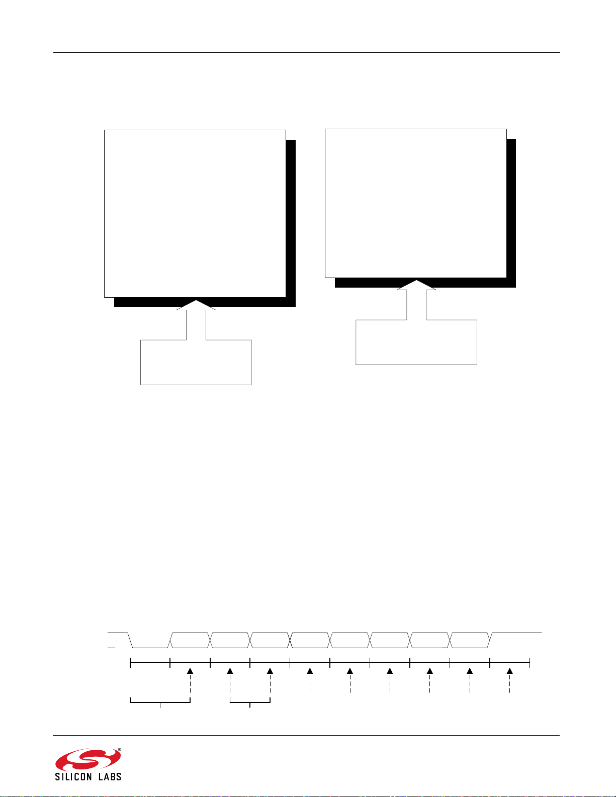
Figure 1. T ransmit and Receive State Machines
State 0
: Transmit START bit.
- Drop TX pin as START condition.
- Update Baud Rate source for next bit time.
- Increment state variable.
State 1-9
:Transmit Bit.
- Shift LSB of Transmit Data onto TX pin.
- Shift STOP bit into MSB of Transmit Data.
- Update Baud Rate source for next bit time.
- Increment state variable.
State 10
: STOP bit transmitted.
- Indicate Transmit complete.
- Trigger user-level interrupt if enabled.
- Reset Transmitter to Idle state.
Transmit State Machine
Interrupt Sources
State 0
: Start bit detected.
- Load Baud Rate source f or 3/2 bit time.
- Increment state variable.
State 1-8
: Bit Received.
- Shift value of RX pin into RX shift register.
- Update Baud Rate source for next bit time.
- Increment state variable.
State 9
: Capture STOP bit.
- Indicate Receive complete.
- Trigger user-level interrupt if enabled.
- Reset Receiver to Idle state.
Receive State Machine
Interrupt Sources
1) User (begin TX)
2) Bit Time Generator
1) START detection
2) Bit Time Generator
Figure 2. SW UART Bit Timing
D1D0 D2 D3 D4 D5 D6 D7
START
BIT
MARK
STOP
BIT
BIT TIMES
BIT SAMPLING
SPACE
3/2 Bit-Time 1 Bit-Time
machines in the PCA ISR. The state machines are
illustrated in Figure 1.
Receive State Machine
When the SW UART is initialized, the PCA
module 0 is configured for negative-edge capture
mode. Its input, CEX0, is routed via the crossbar to
a GPIO pin (P0.2, SW_RX). With the state
machine in State 0, an interrupt is generated when a
falling edge is detected on SW_RX. Since the module is in capture mode, the contents of the PCA
counter are loaded into the module 0 capture registers. Note that this value is independent of interrupt
latency. Module 0 is switched to software timer
mode after the START bit is detected, and 3/2 bittime is added to the module 0 capture register. The
extra 1/2 bit-time is used only after the start bit is
detected, so that sampling will occur during the
middle of the next bit period (see Figure 2). When
the PCA counter reaches the value held in the
module 0 capture registers, the first bit-sampling
interrupt (LSB in this case) occurs.
States 1-8 execute on module match interrupts. In
each state, bits are sampled from SW_RX and
shifted into the RXSHIFT variable. The PCA
module 0 contents are updated in each state to provide the next bit-time interrupt (1 bit time is added
Rev. 1.1 3
Page 4
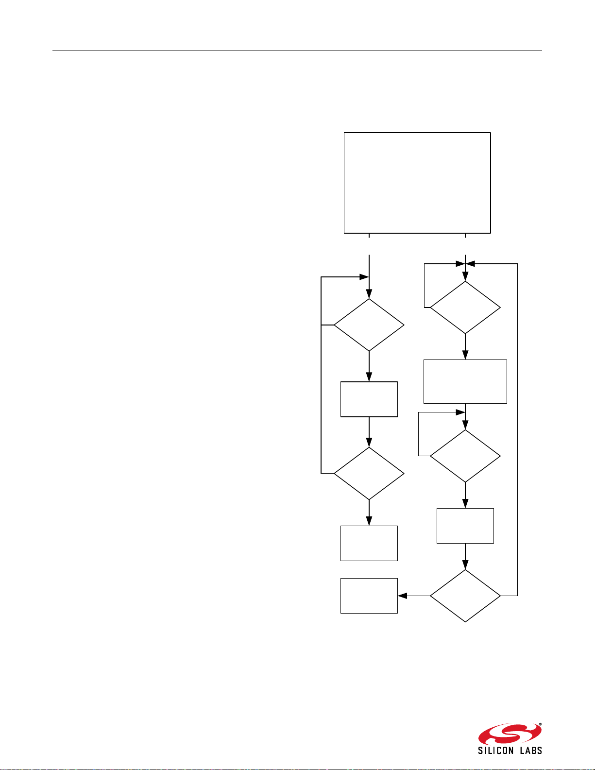
AN115
1) Read RDR.
2) Clear SRI
SRI
1
0
To Receive
STXBSY
1) Write data to TDR.
2) Set CCF1 to
initiate transmit.
3) Set STXBSY
STI
1
0
0
1
To Transmit
Done?
End RX
No
Yes
Done?
NoYes
End TX
Initialization
1) Define SYSCLK and desired
BAUD_RATE.
2) Call SW_UART_INIT.
3) Set SES if user-level interrupt
support is desired.
4) Set SREN to enable th e SW UART
receiver.
5) Call SW_UART_ENABLE.
1) Clear STI
Figure 3. Example 1 User-Level Polled
Mode Interface
to the compare registers). The state variable is also
incremented.
State 9 captures the STOP bit, posts SRI, and
returns the receiver to Idle state.
Transmit State Machine
A user initiates a transmit by forcing a PCA
module 1 interrupt (setting CCF1=1). In State 0,
the TX pin is forced low to generate the START
condition. The PCA counter is read, and this value
plus one bit-time is loaded into to the module 1
capture registers. Note that a few SYSCLKs will
pass between the time the START bit is generated
and when the PCA counter is read. This is the only
instance in Example 1 where interrupt latency
affects the bit time. The effect is negligible (worst
case ~ 1/16 bit-time for 57.6 kbps and an
18.432 MHz SYSCLK).
States 1-9 are executed on module match interrupts. In each state, a bit is shifted out of the LSB
of TDR, and a ‘1’ shifted in the MSB of TDR to
represent the STOP bit. One bit time is added to the
PCA module 1 capture registers to generate the
next bit time. After 9 shifts, the data byte + STOP
bit have been transmitted. The Transmit Complete
indicator (STI) is set, the Transmit Busy indicator
(STXBSY) is cleared, and the TX state variable is
reset.
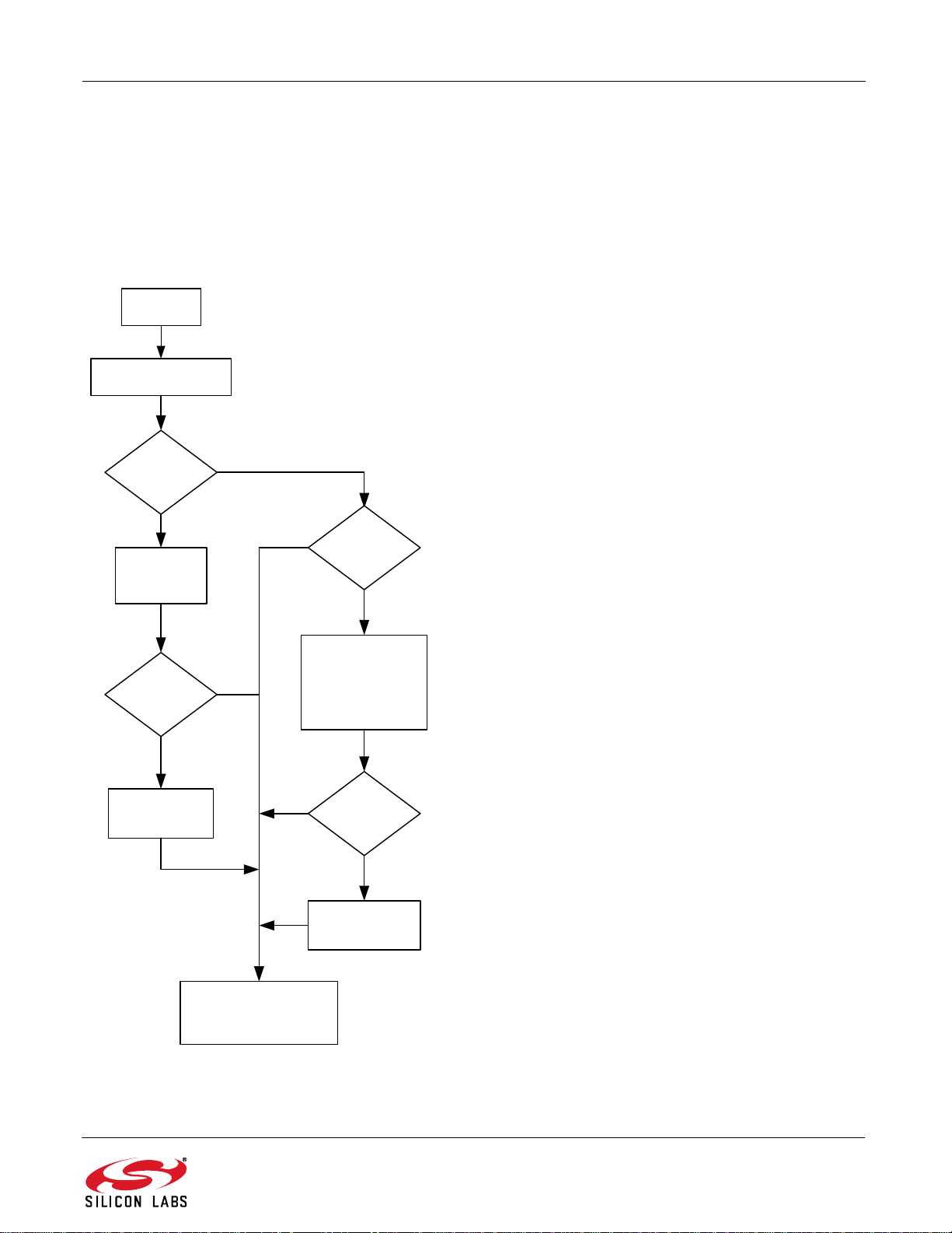
procedure for Example 1 is shown in Figure 3.
Program Interface
The SW UART supports both polled and interruptdriven interfacing. Polled support is configured by
disabling user-level interrupts (SES=0). The transmit and receive indicators (STI and SRI, respectively) can then be polled for transfer completions.
The initialization and polled mode programming
4 Rev. 1.1
The initialization routine, SW_UART_INIT, configures the PCA, interrupts, and state variables for
Page 5
AN115
Figure 4. Example 1 User-Level
Interrupt Mode Interface
Exit ISR
STI || SRI 1) Re-trigger IE7
1
0
1) Read RDR.
2) Clear SRI
SRI
1
0
IE7 Interrupt
STI
1) Clear STI
2) Write new data to
TDR
3) Set CCF1 to
initate transmit.
4) Set STXBSY
Clear IE7 Interrupt
Flag
1
0
Figure 5. Example 1 Test
Configuration
P0.0 (HW_TX)
P0.3 (SW_RX)
P0.1 (HW_RX)
P0.2 (SW_TX)
use in the SW UART. The SW_UART_ENABLE
routine enables the SW UART. The SREN bit must
be set to enable the receiver. Note that the
TIME_COUNT constant is calculated by the software from the BAUD_RATE and SYSCLK constants.
If user-level interrupt support is enabled (SES=1),
an IE7 interrupt is generated each time a transmit
or receive is completed. As with the hardware
UART, user software must check the transmit/
receive complete flags to determine the source of
the interrupt. In the event that a transmit and
receive are completed simultaneously, the user
software will receive only one interrupt. The IE7
ISR must be capable of handling this situation. T w o
options are available: (1) service both transmit and
receive in the same ISR execution, or (2) service
one (STI or SRI) and force an interrupt so that the
ISR is called again to service the other. The second
option is recommended to minimize ISR execution
time.
Test code is provided to interface the SW UART
with the HW UART. Connect jumper wires as
shown in Figure 5.
To use the software in interrupt mode, set SES=1.
The programming procedure for interrupt mode is
shown in Figure 4.
The test code routines configure and enable the
HW UART in Mode 1 using Timer 1 as the baud
rate source. Timer 1 is also configured. Different
baud rates and crystals may be tested by changing
the BAUD_RATE and SYSCLK constants. Both
HW and SW UART baud rate counts are calculated
by the software from these constants. The testing
routines transmit 15 characters in both directions.
Rev. 1.1 5
Page 6

AN115
T o test the SW UART in polled mode, comment the
line
; INTERRUPT_TEST();
and uncomment the line
POLLED_TEST();
Reverse the above steps to test the SW UART in
interrupt mode. Uncomment the line
INTERRUPT_TEST();
And comment the line
; POLLED_TEST();
The longest states in Example 2 require 113
SYSCLKs (TX States 1-9). For an 18.432 MHz
crystal, a SW UART transmit or receive operation
will require a worst case 6 µs per bit transferred
(113*T
bandwidth for a transmit or receive (70% for fullduplex). For the Example 1 software compiled with
the Keil compiler, the full-duplex overhead may be
approximated by the following equation:
FD Overhead(%) ~ = BAUD_RATE/81,000
SYSCLK
). At 57.6 kbps, that’s ~35% of CPU
With Timer 0 in Mode 3, Timer 1 may not set the
TF1 flag, generate an interrupt, or be clocked by
external signals. However, Timer 1 may still operate as a baud rate generator for the HW UART if
configured in Mode 2 (8-bit timer w/auto-reload).
While Timer 0 is in Mode 3, Timer 1 may be
enabled/disabled through its mode settings. Timer
1 is disabled in Mode 3, and enabled in all other
modes.
With Timer 1 as the HW UART baud rate source,
this solution is perhaps the most efficient use of
hardware resources. The downside is increased
software overhead (relative to the 16-bit timer solution). Timer 0 Mode 3 does not offer auto-reload
capabilities; the manual timer reload requires a 16bit move in each interrupt service routine (ISR)
iteration. In addition, interrupt latency will affect
the bit-time accuracy. A correction constant can be
factored into the timer preload values to compensate for typical interrupt latency, but variations in
interrupt latency are unaccounted for.
Slower baud rates may require more than 8-bits of
timer counts for each bit time. With SYSCLK at
18.432 MHz and Timer 0 in SYSCLK/1 mode,
baud rates below 72 kbps require more than 256
timer counts. Available options include:
Per the above equation, baud rates above 80 kbps
are not supported for full duplex operation. The
overhead penalty is only incurred while the SW
UART is performing a transfer. The code listing
begins on page 10.
Example 2: 8-Bit Timer Implementation
In Example1 the SW UART uses Timer0 in
Mode 3. In this mode, Timer 0 is split into two 8bit timers: one is used for transmitting and one for
receiving. TL0 is used as the receive timer; TH0 is
used as the transmit timer.
6 Rev. 1.1
1) Use Timer 0 in SYSCLK/12 mode. Slower baud
rates may be achieved with 8 bits, but standard
baud rate/SYSCLK combinations are more difficult
to obtain.
2) Use Timer 0 in SYSCLK/1 mode, and keep an
upper timer byte manually in the timer ISR. Note
that this method will generate an interrupt every
256 SYSCLKs for each transmit and receive,
regardless of the baud rate (an interrupt each time
the lower 8-bits overflow). The Example 2 software demonstrates option #2.
Program Structure
The transmit and receive operations for Example 2
are implemented as two independent state
Page 7

AN115
machines in the Timer 0 and Timer 1 ISRs (see
Figure 1 on page 3). The Timer 0 ISR is used to
manage the receive state machine; the Timer 1 ISR
manages the transmit state machine. The /INT0
ISR starts the receive state machine, but is disabled
when the receive state is non-zero.
The SW UART receiver captures the START bit
using an external interrupt source, /INT0, configured for active-low edge-sensitive input. The /INT0
interrupt is enabled when waiting for a START bit,
and disabled during transfers. /INT0 is routed to the
GPIO pins via the crossbar. Details on crossbar
configuration can be found in AN001.
Since all timer loading is performed manually in
the ISR, interrupt latency must be compensated for.
A ‘slop constant’ is subtracted from each timer preload value to adjust for this interrupt latency and
code executed between the timer overflow and the
operation of reloading the new timer values. These
constants are independent of the SYSCLK frequency or baud rate; however, they do not account
for variations in interrupt latency.
Implementation
NOTE: For this discussion, assume the baud rate is
slow enough that the 8-bit timers are not sufficient.
The direct RAM bytes labeled BCRHI and BCTHI
are used to manually keep the upper bytes for the
receive and transmit timers, respectively.
Transmit State Machine
When the SW UART is initialized and enabled, the
TX interrupt is set pending but still disabled. The
user initiates the transfer by enabling the transmit
interrupt (Note that TH0, the upper byte of
Timer 0, generates the TX interrupts).
In State 0, the TX pin is asserted low to produce the
START condition, and the timer is loaded with 1 bit
time to produce the next interrupt.
mov TH0, #-LOW(TX_BT);
Notice that BCTHI is loaded with the unsigned bittime high byte, but TH0 is loaded with the negative
of the bit-time low byte. This is because Timer 0
(as all hardware timers) is an up-counter, while
BCTHI counts down. TH0 will overflow and generate an interrupt as it overflows from 0xFF to
0x00; BCTHI is decremented upon each interrupt,
and indicates a bit time when it equals zero.
For States 1-9, one state is executed each time
BCTHI reaches zero. In each State, the LSB of the
Transmit data register (TDR) is shifted onto the TX
pin. The TX timer is loaded with 1 bit time, and a
‘1’ is shifted into the MSB of TDR to represent the
STOP bit in State 9 (TDR should hold 0xFF after
the transfer is complete).
State 10 sets the Transmit Complete indicator
(STI), clears the Transmit Busy indicator
(STXBSY), and triggers an IE7 interrupt if userlevel interrupt support is enabled.
Receive State Machine
In State 0, /INT0 is used as the RX input (configured falling-edge active, HIGH priority). An /INT0
interrupt means a START condition has been
detected. The /INT0 ISR loads the RX timer (TL0
+ BCRHI) with 3/2 bit-time (see Figure 2). BCRHI
is decremented each time TL0 overflows.
States 1-8 execute when BCRHI reaches zero. In
each state, the SW_RX pin is sampled and shifted
into the LSB of the RXSHIFT variable. The RX
timer is also reloaded to generate the next sampling
time. State 9 captures the STOP bit, but framing
error detection is not provided (the STOP bit polarity is not checked). If user-level interrupts are
enabled, this state enables and triggers the IE7
interrupt.
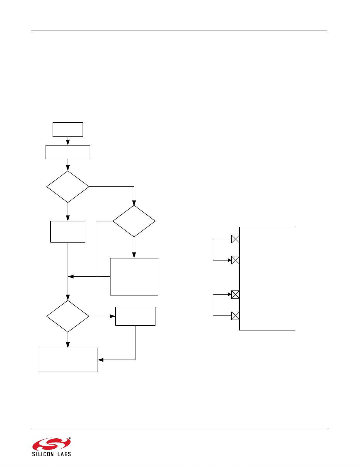
Program Interface
; Load high byte into BCTHI
mov BCTHI, #HIGH(TX_BT);
; Load low byte into TH0
Example 2 supports both polled and interrupt
driven interfacing. The initialization ritual and programming procedure for polled mode is shown in
Rev. 1.1 7
Page 8
AN115
Figure 6. Example 2 User-Level Polled
Mode Interface
Initialization
1) Define TIME_COUNT according to
desired baud rate and SYSCLK.
2) Call SW_UART_INIT .
3) Set SES if user-level interrupt
support is desired.
4) Set SREN to enable the SW UART
receiver.
5) Call SW_UART_ENABLE.
1) Read RDR.
2) Clear SRI
SRI
1
0
To Receive
STXBSY
1) Write data to TDR.
2) Set ETI to initiate
transmit.
3) Set STXBSY
STI
1
0
1) Clear STI
0
1
To Transmit
Done?
End RX
End TX Done?
NoYes
Yes
No
Figure 6. The TIME_COUNT constant must be
explicitly defined in this example.
8 Rev. 1.1
Page 9
AN115
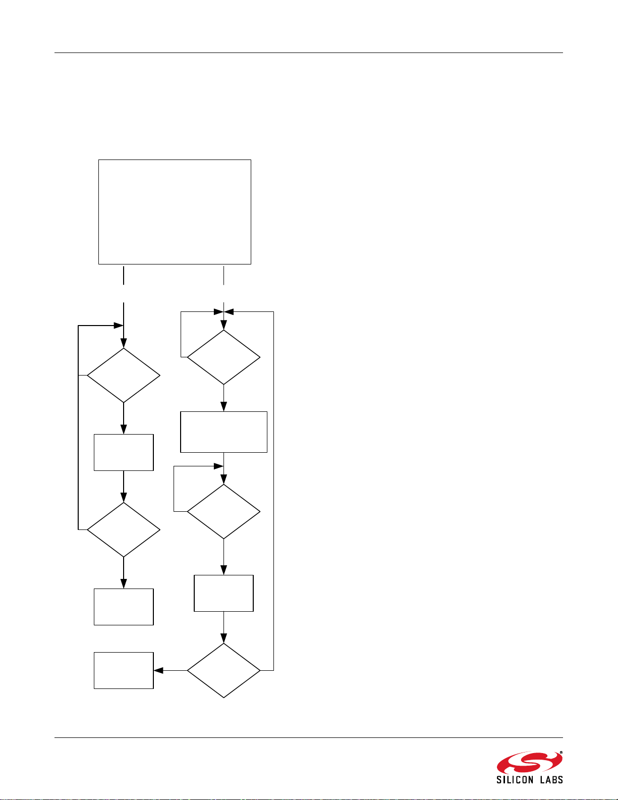
Figure 7. Example 2 User-Level
Interrupt Interface
Exit ISR
STI
1) Re-trigger IE7
1
0
1) Read RDR.
2) Clear SRI
SRI
1
0
IE7 Interrupt
STI
1) Clear STI
2) Write new data to
TDR
3) Set ETI to initate
transmit.
4) Set STXBSY
SRI
1) Re-trigger IE7
1
0
Clear IE7 Interrupt Flag
0
1
Figure 7 shows the IE7 ISR programming sequence
for interrupt mode. Note that the receive operation
is serviced first, since it is the most sensitive to
latency.
one function and re-triggers itself to service the
other.
T est code is provided. To test the polled mode code,
in the MAIN routine uncomment the line
ajmp PolledRX_PolledTX
and comment the line
; ajmp InterruptRX_InterruptTX
To run the interrupt mode test code, reverse the
above steps. Comment the line
; ajmp PolledRX_PolledTX
and uncomment the line
ajmp InterruptRX_InterruptTX
Adding a jumper wire between SW_GPIO_TX and
SW_GPIO_RX provides quick and easy evaluation
of the SW UART. Note that this evaluation method
is only useful with the interrupt mode test code.
To handle the situation of a transmit and receive
completing simultaneously, this example services
With a SYSCLK of 18.432 MHz, the software
given in Example 2 operates in full-duplex at a
maximum of 57.6 kbps. The code listing begins on
page 21.
Rev. 1.1 9
Page 10

AN115
//-----------------------------------------------------------------------------------//
// Copyright 2003 Cygnal, Inc.
//
// FILE NAME: AN015_1.c
// TARGET DEVICE: C8051F00x, C8051F01x
// CREATED ON: 03/10/01
// CREATED BY: JS
//
// Software UART program, using PCA as baud rate source.
// PCA module 0 is used as receive baud rate source and START detector. For START
// detection, module 0 is configured in negative-edge capture mode. For all other
// SW_UART operations, module 0 is configured as a software timer. Module match
// interrupts are used to generate the baud rate. Module 1 generates the transmit
// baud rate in software timer mode.
// Code assumes an external crystal is attached between the XTAL1 and XTAL2 pins.
// The frequency of the external crystal should be defined in the SYSCLK constant.
//
// INITIALIZATION PROCEDURE:
// 1) Define SYSCLK according to external crystal frequency.
// 2) Define desired BAUD_RATE.
// 3) Call SW_UART_INIT().
// 4) Set SREN to enable SW_UART receiver.
// 5) Set SES only if user-level interrupt support is desired.
// 6) Call SW_UART_ENABLE().
//
// TO TRANSMIT:
// 1) Poll STXBSY for zero.
// 2) Write data to TDR.
// 3) Set CCF1 to initiate transmit.
// 4) STI will be set upon transmit completion. An IE7 interrupt is generated if
// user-level interrupts are enabled.
//
// TO RECEIVE:
// 1) If in polled mode, poll SRI. If in interrupt mode, check SRI in IE7 Interrupt
// Service Routine.
// 2) Read data from RDR.
//
// Test code is included, for both polled and interrupt mode. Test code assumes
// the HW_UART pins and SW_UART pins are connected externally:
// P0.0 (HW_UART TX) -> P0.3 (SW_UART RX)
// P0.1 (HW_UART RX) -> P0.2 (SW_UART TX)
//
// To use the test code in polled mode, comment out the call to the INTERRUPT_TEST()
// at the bottom of the main routine, and uncomment the call to POLLED_TEST(). To
// test the interrupt mode, comment out the POLLED_TEST() call and uncomment the
// INTERRUPT_TEST() call.
//
// The test routines configure the HW_UART to operate with Timer 1 as the baud rate
// source. The Timer 1 preload values are auto-calculated from the SYSCLK and BAUD_RATE
// constants.
//
//----------------------------------------------------------------------------------// Includes
//----------------------------------------------------------------------------------#include <c8051f000.h> // SFR declarations
//----------------------------------------------------------------------------------// Global CONSTANTS
10 Rev. 1.1
Page 11

AN115
//-----------------------------------------------------------------------------------
#define BAUD_RATE 57600 // User-definable SW_UART baud rate
#define SYSCLK 18432000 // System clock derived from
// 18.432MHz XTL
#define TIME_COUNT SYSCLK/BAUD_RATE/4 // Number of PCA counts for one
// bit-time. (PCA configured to count
// SYSCLK/4)
#define TH_TIME_COUNT TIME_COUNT*3/2 // 3/2 bit-time, for use after receiving
// a START bit. RX should be LOW for one
// bit-time after the edge of the START,
// and the first bit sample starts in
// the middle of the next bit-time.
#define HW_TIME_COUNT SYSCLK/BAUD_RATE/16 // Time count for HW_UART baud rate
// generation. Auto-calculated from the
// SYSCLK and BAUD_RATE constants
// defined above.
//----------------------------------------------------------------------------------//Global VARIABLES
//-----------------------------------------------------------------------------------
bit SRI; // SW_UART Receive Complete Indicator
bit STI; // SW_UART Transmit Complete Indicator
bit STXBSY; // SW_UART TX Busy flag
bit SREN; // SW_UART RX Enable
bit SES; // SW_UART User-level Interrupt
// Support Enable
sbit SW_RX = P0^2; // SW_UART Receive pin
sbit SW_TX = P0^3; // SW_UART Transmit pin
char TDR; // SW_UART TX Data Register
char RDR; // SW_UART RX Data Register (latch)
// Test Variables
char k, m; // Test indices.
char idata SW_BUF[20]; // SW_UART test receive buffer.
bit HW_DONE; // HW transfer complete flag
// (15 characters transmitted.)
bit SW_DONE; // SW transfer complete flag
// (15 characters transmitted.)
//-----------------------------------------------------------------------------------// Function PROTOTYPES
//------------------------------------------------------------------------------------
void SW_UART_INIT(); // SW_UART initialization routine
void SW_UART_ENABLE(); // SW_UART enable routine
void PCA_ISR(); // SW_UART interrupt service routine
void INTERRUPT_TEST(void); // SW_UART test routine (interrupt mode)
void POLLED_TEST(void); // SW_UART test routine (polled mode)
void USER_ISR(void); // SW_UART test interrupt service
// routine
void HW_UART_INIT(void); // HW_UART initialization and setup
Rev. 1.1 11
Page 12

AN115
// routine
void HW_UART_ISR(void); // HW_UART interrupt service routine
//-----------------------------------------------------------------------------------// MAIN Routine
//-----------------------------------------------------------------------------------// - Disables Watchdog Timer
// - Configures external crystal; switches SYSCLK to external crystal when stable.
// - Configures crossbar and ports.
// - Initializes and enables SW_UART.
// - Calls Test Routines.
//
void MAIN (void){
int delay; // Delay counter.
OSCXCN = 0x66; // Enable external crystal
WDTCN = 0xDE; // disable watchdog timer
WDTCN = 0xAD;
// Port Setup
XBR0 = 0x0C; // HW_UART routed to pins P0.0 and P0.1;
// CEX0 routed to pin P0.2.
XBR2 = 0x40; // Enable crossbar, pull-ups enabled.
PRT0CF = 0x09; // P0.0 (HW TX), and P0.3 (SW TX)
// configured for push-pull output.
delay=256; // Delay >1 ms before polling XTLVLD.
while(delay--);
while (!(OSCXCN & 0x80)); // Wait until external crystal has
// started.
OSCICN = 0x0C; // Switch to external oscillator
OSCICN = 0x88; // Disable internal oscillator; enable
// missing clock detector.
POLLED_TEST(); // Call Polled mode SW_UART test
// routine.
// INTERRUPT_TEST(); // Call Interrupt mode SW_UART test
// routine.
while(1); // Spin forever
}
//-----------------------------------------------------------------------------------// Functions
//------------------------------------------------------------------------------------
//-----------------------------------------------------------------------------------// INTERRUPT_TEST: SW_UART Interrupt Mode Test
// Test code to transmit and receive 15 characters to/from the HW_UART (in interrupt
// mode), with SW_UART in interrupt mode.
// - Initializes and enables the SW_UART & HW_UART
// - Clears all test variables & counters
// - Transfers 15 characters from HW to SW_UART, and 15 characters from SW to HW_UART,
// simultaneously.
//
void INTERRUPT_TEST(void){
12 Rev. 1.1
Page 13

SW_UART_INIT(); // Initialize SW_UART
SW_UART_ENABLE(); // Enable SW_UART
SREN = 1; // Enable SW_UART Receiver
SES = 1; // User-level interrupt support enabled.
HW_UART_INIT(); // Configure HW_UART for testing
// routine.
k=m=0; // Clear user ISR counters.
HW_DONE=0; // Clear transfer complete indicators
SW_DONE=0; //
IE |= 0x10; // Enable HW_UART interrupts
STI = 1; // Indicate transmit complete to
// initiate first transfer.
EIE2 |= 0x20; // Start SW_TX by enabling
PRT1IF |= 0x80; // and forcing an IE7 interrupt
TI = 1; // Initiate a HW_UART transmit
// by forcing TX interrupt.
while(!(HW_DONE&SW_DONE)); // Wait for transfers to finish.
}
AN115
//-----------------------------------------------------------------------------------// POLLED_TEST: SW_UART Polled Mode Test
// Test code to transmit and receive 15 characters to/from the HW_UART, with SW_UART
// in polled mode.
// - Initializes and enables the SW_UART & HW_UART
// - Clears all test variables & counters
// - Sends 15 characters from the HW_UART to be received by SW_UART.
// - Sends 15 characters from the SW_UART to be received by the HW_UART.
//
void POLLED_TEST(void){
SW_UART_INIT(); // Initialize SW_UART
SW_UART_ENABLE(); // Enable SW_UART
SREN = 1; // Enable SW_UART Receiver
SES = 0; // Disable user-level interrupt support.
HW_UART_INIT(); // Configure HW_UART for testing
// routine.
k=m=0; // Clear test counter variables.
HW_DONE = 0; // Clear transfer complete indicators
SW_DONE = 0; //
IE |= 0x10; // Enable HW_UART interrupts.
TI = 1; // Initiate a HW_UART transmit
// by forcing TX interrupt.
// Receive 15 characters with SW_UART; transmit with HW_UART.
while(SREN){ // Run while SW_UART Receiver
// is enabled.
if (SRI){ // If Receive Complete:
SR = 0; // Clear receive flag.
SW_BUF[k++] = RDR; // Read receive buffer.
if (k==15) // If 15 characters have been received:
SREN = 0; // Disable SW_UART Receiver.
Rev. 1.1 13
Page 14

AN115
} // Indicate 15 characters received
}
// Transmit 15 characters with SW_UART; receive with HW_UART.
while(STXBSY); // Poll Busy flag.
STXBSY = 1; // Claim SW_UART Transmitter
TDR=m++; // Load TX data.
CCF1=1; // Initiate first SW_UART TX
// by forcing a PCA module 1 interrupt.
while(!SW_DONE){ // SW_UART transmitting here
// HW_UART receiving.
if (STI){ // If Transmit Complete:
STI = 0; // Clear transmit flag.
if (m<16){ // Transmit 15 characters.
STXBSY = 1; // Claim SW_UART Transmitter
TDR = m++; // Transmit, increment variable.
CCF1 = 1; // Force module 1 interrupt to
} // initiate TX.
else // If this is 15th character,
SW_DONE=1; // Indicate last character transmitted.
}
}
}
//-----------------------------------------------------------------------------------// HW_UART_INIT: HW_UART Initialization Routine
// Sets up HW_UART for use in SW_UART testing.
// - HW_UART in Mode 1
// - Timer 1 used as baud rate source, clocked by SYSCLK.
//
void HW_UART_INIT(void) {
PCON |= 0x80; // SMOD=1 (HW_UART uses Timer 1 overflow
// with no divide down).
TMOD = 0x20; // Configure Timer 1 for use by HW_UART
CKCON |= 0x10; // Timer 1 derived from SYSCLK
TH1 = -HW_TIME_COUNT; // Timer 1 initial value
TL1 = -HW_TIME_COUNT; // Timer 1 reload value
TR1 = 1; // Start Timer 1
RI=0; // Clear HW_UART receive and transmit
TI=0; // complete indicators.
SCON = 0x50; // Configure HW_UART for Mode 1,
// receiver enabled.
}
//-----------------------------------------------------------------------------------// SW_UART_INIT: SW_UART initialization routine
// Prepares SW_UART for use.
// - Configures PCA: Module 0 in negative capture mode; module 1 in software
// timer mode; PCA time base = SYSCLK/4; PCA interrupt disabled; PCA counter
// disabled.
// - Clears pending PCA module 0 and 1 interrupts
// - Resets TX and RX state variables
//
14 Rev. 1.1
Page 15

AN115
void SW_UART_INIT(void){
PCA0CPM0 = 0x10; // Module 0 in negative capture mode;
// module 0 interrupt disabled.
PCA0CPM1 = 0x48; // Module 1 in software timer mode;
// module 1 interrupt disabled.
PCA0CN = 0; // Leave PCA disabled
PCA0MD = 0x02; // PCA timebase = SYSCLK/4; PCA counter
// interrupt disabled.
CCF0 = 0; // Clear pending PCA module 0 and
CCF1 = 0; // module 1 capture/compare interrupts.
SRI = 0; // Clear Receive complete flag.
STI = 0; // Clear Transmit complete flag.
SW_TX = 1; // TX line initially high.
STXBSY = 0; // Clear SW_UART Busy flag
}
//-----------------------------------------------------------------------------------// SW_UART_ENABLE: SW_UART Enable Routine
// Enables SW_UART for use.
// - Enables PCA module 0 interrupts
// - Enables PCA module 1 interrupts
// - Starts PCA counter.
//
void SW_UART_ENABLE(void){
PCA0CPM0 |= 0x01; // Enable module 0 (receive) interrupts.
PCA0CPM1 |= 0x01; // Enable module 1 (transmit)
// interrupts.
CR = 1; // Start PCA counter.
EIE1 |= 0x08; // Enable PCA interrupts
EA = 1; // Globally enable interrupts
}
//-----------------------------------------------------------------------------------// Interrupt Service Routines
//-----------------------------------------------------------------------------------//
// PCA_ISR: PCA Interrupt Service Routine.
// This ISR is triggered by both transmit and receive functions, for each bit that
// is transmitted or received.
// - Checks module 0 interrupt flag (CCF0); if set, services receive state.
// - Checks module 1 interrupt flag (CCF1); if set, services transmit state.
//
void PCA_ISR(void) interrupt 9 {
static char SUTXST = 0; // SW_UART TX state variable
static char SURXST = 0; // SW_UART RX state variable
static unsigned char RXSHIFT; // SW_UART RX Shift Register
unsigned int PCA_TEMP; // Temporary storage variable for
Rev. 1.1 15
Page 16

AN115
// manipulating PCA module
// high & low bytes.
// Check receive interrupt flag first; service if CCF0 is set.
if (CCF0){
CCF0 = 0; // Clear interrupt flag.
switch (SURXST){
// State 0: START bit received.
// In this state, a negative edge on SW_TX has caused the interrupt,
// meaning a START has been detected and the PCA0CP0 registers have
// captured the value of PCA0.
// - Check for receive enable and good START bit
// - Switch PCA module 0 to software timer mode
// - Add 3/2 bit time to module 0 capture registers to sample LSB.
// - Increment RX state variable.
case 0:
if (SREN & ~SW_RX){ // Check for receive enable and a good
// START bit.
PCA_TEMP = (PCA0CPH0 << 8); // Read module 0 contents into
PCA_TEMP |= PCA0CPL0; // PCA_TEMP.
PCA_TEMP += TH_TIME_COUNT; // Add 3/2 bit times to PCA_TEMP
PCA0CPL0 = PCA_TEMP; // Restore PCA0CPL0 and PCA0CPH0
PCA0CPH0 = (PCA_TEMP >> 8); // with the updated value
PCA0CPM0 = 0x49; // Change module 0 to software
// timer mode, interrupts enabled.
SURXST++; // Update RX state variable.
}
break;
// States 1-8: Bit Received
// - Sample SW_RX pin
// - Shift new bit into RXSHIFT
// - Add 1 bit time to module 0 capture registers
// - Increment RX state variable
case 1:
case 2:
case 3:
case 4:
case 5:
case 6:
case 7:
case 8:
RXSHIFT = RXSHIFT >> 1; // Shift right 1 bit
if (SW_RX) // If SW_RX=1,
RXSHIFT |= 0x80; // shift '1' into RXSHIFT MSB
PCA_TEMP = (PCA0CPH0 << 8); // Read module 0 contents into
PCA_TEMP |= PCA0CPL0; // PCA_TEMP.
PCA_TEMP += TIME_COUNT; // Add 1 bit time to PCA_TEMP
PCA0CPL0 = PCA_TEMP; // Restore PCA0CPL0 and PCA0CPH0
16 Rev. 1.1
Page 17

PCA0CPH0 = (PCA_TEMP >> 8); // with the updated value
SURXST++; // Update RX state variable.
break;
// State 9: 8-bits received, Capture STOP bit.
// - Move RXSHIFT into RDR.
// - Set SRI (indicate receive complete).
// - Prepare module 0 for next transfer.
// - Reset RX state variable.
// - Trigger IE7 if user-level interrupt support is enabled.
case 9:
RDR = RXSHIFT; // Move received data to receive
// register.
SRI = 1; // Set receive complete indicator.
PCA0CPM0 = 0x11; // Switch module 0 to negative capture
// mode; interrupt enabled for START
// detection.
SURXST = 0; // Reset RX state variable.
if (SES){ // If user-level interrupt support
// enabled
EIE2 |= 0x20; // Enable IE7.
PRT1IF |= 0x80; // Trigger IE7.
}
break;
AN115
}
}
// Check Transmit interrupt; service if CCF1 is set.
else if (CCF1){
CCF1 = 0; // Clear interrupt flag
switch (SUTXST){
// State 0: Transmit Initiated.
// Here, the user has loaded a byte to transmit into TDR, and set the
// module 1 interrupt to initiate the transfer.
// - Transmit START bit (drop SW_TX)
// - Read PCA0, add one bit time, & store in module 1 capture registers
// for first bit.
// - Increment TX state variable.
case 0:
SW_TX = 0; // Drop TX pin as START bit.
PCA_TEMP = PCA0L; // Read PCA counter value into
PCA_TEMP |= (PCA0H << 8); // PCA_TEMP.
PCA_TEMP += TIME_COUNT; // Add 1 bit time.
PCA0CPL1 = PCA_TEMP; // Store updated match value into
PCA0CPH1 = (PCA_TEMP >> 8); // module 1 capture/compare registers.
PCA0CPM1 |= 0x48; // Enable module 1 software timer.
Rev. 1.1 17
Page 18

AN115
SUTXST++; // Update TX state variable.
break;
// States 1-9: Transmit Bit.
// - Output LSB of TDR onto TX
// - Shift TDR 1 bit right.
// - Shift a '1' into MSB of TDR for STOP bit in State 9.
// - Add 1 bit time to module 1 capture register
case 1:
case 2:
case 3:
case 4:
case 5:
case 6:
case 7:
case 8:
case 9:
SW_TX = (TDR & 0x01); // Output LSB of TDR onto SW_TX pin.
TDR >>= 1; // Shift TDR right 1 bit.
TDR |= 0x80; // Shift '1' into MSB of TDR for
// STOP bit in State 9.
PCA_TEMP = (PCA0CPH1 << 8); // Read module 1 contents into
PCA_TEMP |= PCA0CPL1; // PCA_TEMP.
PCA_TEMP += TIME_COUNT; // Add 1 bit time to PCA_TEMP
PCA0CPL1 = PCA_TEMP; // Restore PCA0CPL1 and PCA0CPH1
PCA0CPH1 = (PCA_TEMP >> 8); // with the updated value
SUTXST++; // Update TX state variable.
break;
// State 10: Last bit has been transmitted. Transmit STOP bit
// and end transfer.
// - Transmit STOP bit
// - Set TX Complete indicator, clear Busy flag
// - Reset TX state
// - Prepare module 1 for next transfer.
// - Trigger IE7 interrupt if user-level interrupts enabled.
case 10:
STI = 1; // Indicate TX complete.
SUTXST = 0; // Reset TX state.
SW_TX = 1; // SW_TX should remain high.
PCA0CPM1 = 0x01; // Disable module 1 software timer;
// leave interrupt enabled for next
// transmit.
if (SES){ // If user-level interrupt support
// enabled:
EIE2 |= 0x20; // Enable IE7.
PRT1IF |= 0x80; // Trigger IE7.
}
STXBSY = 0; // SW_UART TX free.
break;
}
18 Rev. 1.1
Page 19

AN115
}
}
//-----------------------------------------------------------------------------------// USER_ISR: User SW_UART Interrupt Service Routine (IE7 ISR)
// If interrupt-mode test code is enabled, this ISR
// transmits 15 characters and receives 15 characters. This routine is triggered each
// time a SW_UART transmit or receive is completed.
// - Checks receive complete indicator, and services.
// - Checks transmit complete indicator, and services.
// - Checks for transmits or receives that completed during the ISR; if so, triggers the
// interrupt again.
//
void USER_ISR(void) interrupt 19 { // IE7 Interrupt Service Routine
PRT1IF &= ~(0x80); // Clear IE7 interrupt flag
if (SRI){ // If Receive Complete:
SRI = 0; // Clear receive flag.
SW_BUF[k++] = RDR; // Read receive buffer.
if (k==15){ // If 15 characters have been received:
SREN=0; // Disable SW_UART Receiver.
} // Indicate 15 characters received.
}
else if (STI){ // If Transmit Complete:
STI = 0; // Clear transmit flag.
if (m<15){ // If less than 15 characters:
STXBSY = 1; // Claim SW_UART Transmitter.
TDR = m++; // Increment variable, transmit.
CCF1 = 1; // Force module 1 interrupt to initiate
} // TX
else
SW_DONE=1; // Indicate last character transmitted.
}
if (STI|SRI) // If SRI or STI is set, re-trigger
PRT1IF |= 0x80; // interrupt to service.
}
//-----------------------------------------------------------------------------------// HW_UART_ISR: Hardware UART Interrupt Service Routine
// Transmits characters from 1 to 15, and receives 15 characters.
// - Checks receive interrupt, and services.
// - Checks transmit interrupt, and services.
//
void HW_UART_ISR(void) interrupt 4 {
static char i=0; // Transmit data variable.
static char j=0; // Receive data index.
static idata char HW_BUF[20]; // Receive data buffer.
if (RI){ // If Receive Complete:
RI=0; // Clear receive flag
HW_BUF[j++] = SBUF; // Read receive buffer
if (j==15) // If 15 characters received:
REN=0; // Disable HW_UART receiver.
Rev. 1.1 19
Page 20

AN115
}
else if (TI){ // If Transmit Complete:
TI = 0; // Clear transmit flag
if (i<15) // If characters left to transmit:
SBUF=i++; // Increment variable, transmit.
else // If 15 characters transmitted,
HW_DONE=1; // Indicate HW TX finished.
}
}
// End of Example 1, Software UART with PCA
20 Rev. 1.1
Page 21

;----------------------------------------------------------------------------; Cygnal, INC.
;
;
; FILE NAME : AN015_2.ASM
; TARGET MCU : C8051F0xx
; DESCRIPTION : Example source code for a software UART
;
; IMPLEMENTATION NOTES:
; - uses Timer0 in Mode3 (two 8-bit timers)
; - Timer0 run/overflow is used for RX state machine
; - Timer1 overflow is used for TX state machine
; - 8N1, no Framing error detection
; - uses IE7 as user-level interrupt
; - uses single-byte PC offset for state table implementation
; - uses /INT0 falling as START bit detect (primitive START bit verification)
;
;-----------------------------------------------------------------------------
;----------------------------------------------------------------------------; EQUATES
;-----------------------------------------------------------------------------
$MOD8F000
AN115
; SW UART constants
SW_TX_GPIO EQU P0.4 ; SW UART TX GPIO pin (can be any GPIO pin)
SW_RX_GPIO EQU P0.2 ; SW UART RX GPIO pin (must be /INT0)
TIME_COUNT EQU 320
; Note: 320 is the limit for reliable
; FD operation...
; FOR SYSCLK = 18.432 MHz:
; 115200 = 160
; 57600 = 320
; 38400 = 480
; 19200 = 960
; 9600 = 1920
; 4800 = 3840
; 2400 = 7680
TX_CORR EQU 41 ; (41) Timer preload correction value in
; cycles for TX
RX_CORR EQU 47 ; (47) Timer preload correction value in
; cycles for RX
THALF_CORR EQU 113 ; (113)Timer preload correction value for
; 3/2 RX
TX_BT EQU TIME_COUNT - TX_CORR; actual 16-bit bit counter cycle value
; TX
RX_BT EQU TIME_COUNT - RX_CORR; actual 16-bit bit counter cycle value
; RX
THALF_BT EQU TIME_COUNT*3/2 - THALF_CORR ; actual 16-bit 1.5 bit cycle value
; RX
RX_BUFSIZE EQU 16 ; size of RX buffer in chars
;----------------------------------------------------------------------------; VARIABLES
;-----------------------------------------------------------------------------
Rev. 1.1 21
Page 22

AN115
BSEG
org 0h
SRI: DBIT 1 ; SW UART Receive complete flag
STI: DBIT 1 ; SW UART Transmit complete flag
STXBSY: DBIT 1 ; SW UART TX BSY flag
SREN: DBIT 1 ; SW UART RX Enable
SES: DBIT 1 ; SW UART user-Interrupt Support Enable
DSEG at 30h
TDR: DS 1 ; SW UART TX data register
RDR: DS 1 ; SW UART RX data register
RXSHIFT: DS 1 ; SW UART RX shift register
SURXST: DS 1 ; SW UART RX state variable
SUTXST: DS 1 ; SW UART TX state variable
BCRHI: DS 1 ; MSB of 16-bit bit timer for SW UART RX
BCTHI: DS 1 ; MSB of 16-bit bit timer for SW UART TX
;test variables
RX_TAIL: DS 1 ; write pointer to RX message buffer
TX_VAL: DS 1 ; value to transmit
;------------------; Indirect address space variables
ISEG at 80h
RX_BUF: DS RX_BUFSIZE ; RX message buffer
;------------------; STACK
STACK_TOP: DS 1 ; placeholder in symbol table for
; beginning of hardware stack
;----------------------------------------------------------------------------; MACRO DEFINITIONS
;-----------------------------------------------------------------------------
;----------------------------------------------------------------------------; RESET AND INTERRUPT VECTOR TABLE
;-----------------------------------------------------------------------------
CSEG
org 00h
ljmp Reset ; RESET initialization vector
org 03h
ljmp INT0_ISR ; Software UART RX START bit detect
org 0bh
ljmp Timer0_ISR ; Software UART RX state machine interrupt
org 1bh
ljmp Timer1_ISR ; Software UART TX state machine interrupt
org 9bh
ljmp IE7_ISR ; user-level Software UART interrupt
22 Rev. 1.1
Page 23

;----------------------------------------------------------------------------; MAIN PROGRAM CODE
;-----------------------------------------------------------------------------
org 0B3h
Main:
ajmp PolledRX_PolledTX ; leave one of these lines uncommented
; ajmp InterruptRX_InterruptTX; leave one of these lines uncommented
sjmp $ ; spin forever...
;----------------------------------------------------------------------------; MAIN SUBROUTINES
;-----------------------------------------------------------------------------
;----------------------------------------------------------------------------; PolledRX_PolledTX
;----------------------------------------------------------------------------; This routine demonstrates polled access to the SW UART.
;
; The transmitter transmits a sequence from $00 to $ff
;
; The receiver receives characters and stores them in a circular buffer.
;
PolledRX_PolledTX:
acall SW_UART_Init ; initialize SW UART (leave in a
; disabled state)
AN115
setb SREN ; enable SW UART receiver
clr SES ; disable user-level interrupt
; support
acall SW_UART_Enable ; enable SW UART
; transmit message -- polled mode
jb STXBSY, $ ; wait for SW TX available
; transmit chars $00 to $ff
clr a
TX_LOOP: setb STXBSY ; claim SW UART Transmitter
mov TDR, a ; write char to transmit data reg
setb ET1 ; initiate SW TX operation
inc a ; set next value to write
jnb STI, $ ; wait for TX complete
clr STI ; clear TX complete indicator
jnz TX_LOOP
TX_LOOP_END:
mov RX_TAIL, #RX_BUF ; initialize TAIL pointer
; receive message -- polled mode
RX_LOOP: mov r0, RX_TAIL ; indirect address to write character to
jnb SRI, $ ; wait for RX character
clr SRI ; clear RX complete indicator
mov @r0, RDR ; store it
inc RX_TAIL ; advance TAIL pointer
mov a, RX_TAIL ; handle TAIL wrapping
add a, #-(RX_BUF + RX_BUFSIZE)
Rev. 1.1 23
Page 24

AN115
jnc RX_LOOP
mov RX_TAIL, #RX_BUF ; wrap TAIL
sjmp RX_LOOP ; repeat forever...
;----------------------------------------------------------------------------; InterruptRX_InterruptTX
;----------------------------------------------------------------------------; This routine demonstrates interrupt access to the SW UART.
;
; The receiver receives characters and stores them in a circular buffer.
; Both the transmit and receive routines are located in the IE7_ISR handler.
;
InterruptRX_InterruptTX:
acall SW_UART_Init ; initialize SW UART (leave in a
; disabled state)
setb SES ; Enable user-level interrupt support
setb SREN ; Enable SW UART receiver
mov RX_TAIL, #RX_BUF ; initialize TAIL pointer
acall SW_UART_Enable ; enable SW UART
setb STI ; kick-start SW UART transmitter
orl EIE2, #00100000b ; by enabling IE7
orl PRT1IF, #10000000b ; and activating IE7
sjmp $
;----------------------------------------------------------------------------; INTERRUPT VECTORS
;----------------------------------------------------------------------------;----------------------------------------------------------------------------; Reset Interrupt Vector
;
; This routine initializes the device and all peripherals and variables.
; - External oscillator started (SYSCLK will be switched to external osc.
; once XTLVLD goes high)
; - Watchdog timer is disabled
; - Crossbar and GPIO output modes are defined
; - H/W stack pointer is initialized
; - interrupt priorities and enables are initialized here
; - /INT0
; - Timer0
; - Timer1
Reset:
mov OSCXCN, #01100110b ; Enable Crystal osc., divide by 1 mode
; XFCN = '110' for 18.432 MHz crystal
; External oscillator will be selected
; below after XTLVLD has gone high
; indicating that the external osc
; has started and settled (several
; hundred microseconds from now).
mov WDTCN, #0deh ; disable watchdog timer
mov WDTCN, #0adh
24 Rev. 1.1
Page 25

OSC_WAIT:
AN115
; set up Crossbar and Port I/O
mov XBR0, #00000100b ; enable HW UART on P0.0 (TX), P0.1 (RX)
mov XBR1, #10000100b ; enable /INT0 on P0.2; /SYSCLK on P0.3
mov XBR2, #01000000b ; enable crossbar w/ pull-ups enabled
orl PRT0CF, #00011101b ; enable P0.0, 0.2, 0.3, and 0.4 as push-pull
; P0.4 is SW UART TX pin
; P0.2 is SW UART RX pin
orl PRT1CF, #01000000b ; enable P1.6 (LED on target board) as
; push-pull
mov SP, #STACK_TOP ; init stack pointer to end of allocated RAM
; Wait >1 ms before checking external crystal for stability
clr a
mov r0, a ; Clear r0
djnz r0, $ ; Delay ~380 µs
djnz r0, $ ; Delay ~380 µs
djnz r0, $ ; Delay ~380 µs
mov a, OSCXCN ; spin here until crystal osc is stable
jnb acc.7, OSC_WAIT
orl OSCICN, #00001000b ; Select external osc. as
; system clock source
anl OSCICN, #NOT(00000100b); Disable internal oscillator
orl OSCICN, #10000000b ; Enable missing clock detector
; this must be done AFTER
; selecting external osc as system
; clock source
setb EA ; enable GLOBAL interrupts
ljmp Main
;----------------------------------------------------------------------------; Timer0_ISR / INT0_ISR
;
; These interrupts start and drive the SW UART receive state machine
;
SWRX_STATE_TABLE: ; each table entry is 1 byte
DB SWRX_S0 - SWRX_STATE_TABLE ; IDLE / START detect
DB SWRX_S1 - SWRX_STATE_TABLE ; b0
DB SWRX_S2 - SWRX_STATE_TABLE ; b1
DB SWRX_S3 - SWRX_STATE_TABLE ; b2
DB SWRX_S4 - SWRX_STATE_TABLE ; b3
DB SWRX_S5 - SWRX_STATE_TABLE ; b4
DB SWRX_S6 - SWRX_STATE_TABLE ; b5
DB SWRX_S7 - SWRX_STATE_TABLE ; b6
DB SWRX_S8 - SWRX_STATE_TABLE ; b7
DB SWRX_S9 - SWRX_STATE_TABLE ; STOP bit capture
INT0_ISR:
Timer0_ISR:
push PSW ; resource preservation
push acc
Rev. 1.1 25
Page 26

AN115
mov a, BCRHI ; if BCRHI is non-zero, we need to roll
; through the timer again...
jz SWRX_PROCESS_STATE
dec BCRHI
ajmp Timer0_ISR_EXIT
SWRX_PROCESS_STATE:
push DPH ; resource preservation
push DPL
mov a, SURXST ; read state offset from table
mov DPTR, #SWRX_STATE_TABLE
movc a, @A+DPTR ; 'a' now contains state offset (PC)
jmp @A+DPTR ; execute state
Timer0_ISR_END: ; ALL RX states return here
pop DPL ; resource restoration
pop DPH
Timer0_ISR_EXIT:
pop acc ; resource restoration
pop PSW
reti
;SWRX_S0: RX IDLE state
; At this point, a falling edge has been detected on /INT0.
; We first check to see if the SW UART receiver is enabled. If it is, we check
; once to see if the RX pin is still low (START bit valid). If it is, we set up
; Timer0 to count for 3/2 bit time in order to capture the LSB. Here, we also
; disable /INT0 interrupts.
; - Check for SREN = '1': IF '1':
; - Load TL0 with 3/2 bit time value
; - Start Timer
; - Enable TF0 interrupt
; - Disable /INT0 interrupt
; - INC state variable to S1
; - IF SREN = '0' (SW UART RX disabled)
; - exit gracefully, next state is S0
;
SWRX_S0:
jnb SREN, SWRX_S0_END ; Check to see if SW UART RX is enabled
; if not, exit and remain at IDLE state
jb SW_RX_GPIO, SWRX_S0_END; check to see if START bit is good
clr EX0 ; disable /INT0
clr TR0 ; Stop Timer0 (low)
clr TF0 ; Clear any pending interrupts
mov BCRHI, #HIGH(THALF_BT); set Timer0 (low) + BCRHI for 1.5 bit
mov TL0, #-LOW(THALF_BT); times from now (we assume the start
; bit is good)
setb ET0 ; enable Timer0 interrupts
setb TR0 ; Start Timer0L
inc SURXST ; next state is SWRX_S1 (we assume START bit
; is good)
26 Rev. 1.1
Page 27

SWRX_S0_END:
ajmp Timer0_ISR_END
;SWRX_S1 thru SWRX_S8: Capture b0..b7
; At this point, we've determined that the START bit is valid, and we're going to
; query RX_GPIO at bit intervals, shifting the results into RXSHIFT.
; - If BCRHI is non-zero, then we need to spin through the timer again
; - DEC BCRHI
; - let timer roll over on its own
; - leave state as is
; - If BCRHI is zero:
; - stop timer
; - Move RX_GPIO state into Carry
; - Right shift Carry into RXSHIFT
; - set up timer to capture the next bit
; - enable timer
; - advance state variable
;
SWRX_S1:
SWRX_S2:
SWRX_S3:
SWRX_S4:
SWRX_S5:
SWRX_S6:
SWRX_S7:
SWRX_S8:
clr TR0 ; Stop Timer0 (low)
clr TF0 ; Clear any pending interrupts
AN115
mov BCRHI, #HIGH(RX_BT) ; load bit time value into 16-bit virtual
; counter
mov TL0, #-LOW(RX_BT)
setb TR0 ; START RX bit timer
mov C, SW_RX_GPIO ; Move RX state into Carry prior to rshift
mov a, RXSHIFT
rrc a ; right shift Carry into shift register
mov RXSHIFT, a ; re-store
inc SURXST ; advance state variable
SWRX_S2_END:
ajmp Timer0_ISR_END
;SWRX_S9: Capture STOP bit
; At this point, we've shifted all the data bits into RXSHIFT, and we're ready to
; sample the STOP bit. Here, we indicate that we've received a character, and reset
; the state machine back to IDLE. In this implementation, we don't actually capture
; the STOP bit; we assume it's good. Here's where we would add support for Framing
; Error detection.
; - If BCRHI is non-zero, then we need to spin through the timer again
; - DEC BCRHI
; - let timer roll over on its own
; - leave state as is
; - If BCRHI is zero:
; - stop timer
Rev. 1.1 27
Page 28

AN115
; - Move RXSHIFT into RDR
; - Set SRI
; - Disable timer interrupt
; - Enable /INT0 interrupt
; - Reset state variable to IDLE
; - Check to see if User-level interrupt support is enabled (EIS): If so:
; - Enable IE7
; - Toggle P1.7 to activate IE7
;
SWRX_S9:
clr TR0 ; Stop Timer0L
mov RDR, RXSHIFT ; move data from shift reg to data reg
setb SRI ; set SW UART SRI bit to indicate RX complete
clr ET0 ; Disable Timer0L interrupt
clr IE0 ; Disable pending /INT0 interrupts
setb EX0 ; Enable /INT0 interrupt
mov SURXST, #00 ; reset RX state to IDLE
jnb SES, SWRX_S9_END ; check to see if user-level interrupt
; support is enabled
orl EIE2, #00100000b ; enable IE7; leave priority alone
orl PRT1IF, #10000000b ; activate IE7
SWRX_S9_END:
ajmp Timer0_ISR_END
;----------------------------------------------------------------------------; Timer1_ISR (note that this is actually called by the upper-half of Timer0
; which is operating in Mode 3)
;
; This interrupt drives the SW UART transmit state machine
;
SWTX_STATE_TABLE: ; each table entry is 1 byte; 11 entries
; total
DB SWTX_S0 - SWTX_STATE_TABLE; START bit
DB SWTX_S1 - SWTX_STATE_TABLE; b0
DB SWTX_S2 - SWTX_STATE_TABLE; b1
DB SWTX_S3 - SWTX_STATE_TABLE; b2
DB SWTX_S4 - SWTX_STATE_TABLE; b3
DB SWTX_S5 - SWTX_STATE_TABLE; b4
DB SWTX_S6 - SWTX_STATE_TABLE; b5
DB SWTX_S7 - SWTX_STATE_TABLE; b6
DB SWTX_S8 - SWTX_STATE_TABLE; b7
DB SWTX_S9 - SWTX_STATE_TABLE; STOP bit onset edge
DB SWTX_S10 - SWTX_STATE_TABLE; STOP bit terminus
Timer1_ISR:
push PSW ; resource preservation
push acc
mov a, BCTHI ; if BCTHI is non-zero, we need to roll
; through the timer again...
jz SWTX_PROCESS_STATE
dec BCTHI
ajmp Timer1_ISR_EXIT
SWTX_PROCESS_STATE:
push DPH ; resource preservation
28 Rev. 1.1
Page 29

push DPL
mov a, SUTXST ; read state offset from table
mov DPTR, #SWTX_STATE_TABLE
movc a, @A+DPTR ; acc now contains state offset
jmp @A+DPTR ; execute State x
Timer1_ISR_END: ; ALL TX states return here
pop DPL ; resource restoration
pop DPH
Timer1_ISR_EXIT:
pop acc ; resource restoration
pop PSW
reti
;SWTX_S0: TX START bit state
; At this point, user code has placed the char to be transmitted in TDR and has
; called the Timer1 interrupt handler explicitly by setting TF1.
; - Clear STI
; - Drop TX_GPIO (START bit onset edge)
; - Configure TH0, BCTHI for next bit time, which will be the LSB
; - Enable TH0
; - Set next state to SWTX_S1
;
SWTX_S0:
mov BCTHI, #HIGH(TX_BT) ; load bit time value into 16-bit virtual
; counter
mov TH0, #-LOW(TX_BT)
clr SW_TX_GPIO ; START bit onset edge
clr TF1 ; clear any pending interrupts
AN115
inc SUTXST ; next state is SWTX_S1
SWTX_S0_END:
ajmp Timer1_ISR_END
;SWTX_S1 thru SWTX_S9: TX b0..b7 and STOP bit
; At this point, we start shifting the character in TDR out the TX_GPIO pin, bit
; by bit, one bit per state transition. We shift in an extra '1' at the MSB which
; becomes the STOP bit.
; - If BCTHI is non-zero, then we need to spin through the timer again
; - DEC BCTHI
; - let timer roll over on its own
; - leave state as is
; - If BCTHI is zero:
; - stop timer
; - set up timer for next bit
; - right-shift TDR
; - enable timer
; - output bit
; - advance state variable
;
SWTX_S1:
SWTX_S2:
SWTX_S3:
SWTX_S4:
SWTX_S5:
SWTX_S6:
Rev. 1.1 29
Page 30

AN115
SWTX_S7:
SWTX_S8:
SWTX_S9:
mov BCTHI, #HIGH(TX_BT) ; load bit time value into 16-bit virtual
; counter
mov TH0, #-LOW(TX_BT)
mov a, TDR ; right shift next bit to transmit into Carry
setb C ; shift STOP bit into MSB
rrc a
mov TDR, a ; re-store value
mov SW_TX_GPIO, C ; output bit on GPIO pin
clr TF1 ; clear any pending interrupts
inc SUTXST ; advance to next state
SWTX_S1_END:
ajmp Timer1_ISR_END
;SWTX_S10 STOP bit complete / reset to IDLE
; At this point, we've shifted the STOP bit out, and we're ready to reset the state
; machine and indicate transmit complete, including initiating a user-level interrupt
; if it's enabled.
; - If BCTHI is non-zero, then we need to spin through the timer again
; - DEC BCTHI
; - let timer roll over on its own
; - leave state as is
; - If BCTHI is zero:
; - stop timer
; - set STI
; - clear STXBSY
; - check for IE7 support, and activate if enabled
; - set state variable to S0
;
SWTX_S10:
clr ET1 ; Disable Timer1 interrupts
setb TF1 ; Force a pending Timer1 interrupt. This
; allows the Enable Timer1 interrupt
; operation to immediately trigger a
; transmit operation
mov SUTXST, #00h ; reset state variable to IDLE state
setb STI ; Set STI to indicate transmit complete
clr STXBSY ; Clear TXBSY to indicate transmitter
; available
jnb SES, SWTX_S10_END ; activate user-level interrupt IE7 if
; enabled
orl EIE2, #00100000b ; enable IE7; leave priority alone
orl PRT1IF, #10000000b ; activate IE7
SWTX_S10_END:
ajmp Timer1_ISR_END
;----------------------------------------------------------------------------; IE7_ISR
;
; This is the user-level interrupt handler for the SW UART. Note: this code
; MUST check both SRI and TRI, and if both are set, it must handle one case, and
; re-trigger IE7 for the other case (or handle it in the same call) if that case
30 Rev. 1.1
Page 31

; is interrupt handled. This is not required, for example, if the RX case is
; handled in the interrupt and the TX case is polled.
;
; Note, if the TX case is polled, STI should not be cleared here.
;
; In this example, if SRI is set, indicating that a character was received by
; the SW UART, that received character is stored in a circular buffer (RX_BUF).
; If STI is set, indicating transmit complete, the character stored in TX_VAL
; is transmitted (and post incremented).
;
;
IE7_ISR:
push PSW
push acc
anl PRT1IF, #NOT(10000000b); clear IE7
jbc SRI, SW_RX_HANDLE ; handle receive first, since
; it's the most sensitive to
; latency
jbc STI, SW_TX_HANDLE ; handle TX case
IE7_ISR_END:
pop acc
pop PSW
reti ; all IE7_ISR routines return here...
AN115
SW_RX_HANDLE:
push ar0 ; resource preservation
mov r0, RX_TAIL ; point r0 to location to store
mov @r0, RDR ; read value into buffer
inc RX_TAIL ; update the TAIL pointer
mov a, RX_TAIL ; wrap pointer if necessary
add a, #-(RX_BUF+RX_BUFSIZE)
jnc SW_RX_HANDLE_END
mov RX_TAIL, #RX_BUF ; wrap the pointer
SW_RX_HANDLE_END:
jnb STI, NO_TX_PENDING ; if TX interrupt is pending,
orl PRT1IF, #10000000b ; activate it (IE7)
NO_TX_PENDING:
pop ar0
ajmp IE7_ISR_END
SW_TX_HANDLE:
setb STXBSY ; claim SW UART Transmitter
mov TDR, TX_VAL ; load byte to transmit into TDR
setb ET1 ; start SW UART transmitter
inc TX_VAL ; next byte to store
SW_TX_HANDLE_END:
jnb SRI, NO_RX_PENDING ; if RX interrupt is pending,
orl PRT1IF, #10000000b ; activate it (IE7)
NO_RX_PENDING:
ajmp IE7_ISR_END ; exit
;----------------------------------------------------------------------------; SUBROUTINES
;-----------------------------------------------------------------------------
Rev. 1.1 31
Page 32

AN115
;----------------------------------------------------------------------------; SW UART SUBROUTINES (non-user code)
;-----------------------------------------------------------------------------
;----------------------------------------------------------------------------; SW_UART_Init
;
; Init:
; - /INT0 is falling-edge triggered
; - Timer0 in Mode 3, (2) 8-bit timers, interrupt handlers for TL0, TH0 (TF0, TF1)
; timers initially disabled...
; - RX/TX State machines and state variables
; - SW UART TX state machine and RX state machine operate at HIGH priority
SW_UART_Init:
; Init /INT0
clr EX0 ; disable /INT0 interrupts
setb IT0 ; /INT0 is falling-edge triggered
clr IE0 ; forcibly clear /INT0 interrupt flag
setb PX0 ; /INT0 is HIGH priority interrupt
; Init Timer0
clr ET0 ; disable Timer0 interrupts
clr ET1 ; disable Timer1 interrupts
clr TR0 ; Timer0 off
clr TR1 ; Timer1 off
clr TF0 ; forcibly clear interrupt flags
clr TF1
orl TMOD, #00000011b ; Timer0 in Mode 3 (2) 8-bit timers
anl TMOD, #NOT(00001100b); GATE0=0; C/T0 = 0
orl CKCON, #00001000b ; Timer0 uses system clock as time base
setb PT0 ; Timer0 interrupt is HIGH priority
setb PT1 ; Timer1 interrupt is HIGH priority
; User-level interrupt (IE7) is initialized explicitly by the state
; machines
; Init State Machines and Variables
clr a ; Init state machines
mov SURXST, a ; RX state variable
mov SUTXST, a ; TX state variable
mov BCRHI, a ; RX bit timer MSB
mov BCTHI, a ; TX bit timer MSB
clr SES ; Disable user-level interrupt support
clr SREN ; Disable SW UART receiver
clr TXBSY ; clear TXBSY indicator
clr SRI ; clear RX complete indicator
clr STI ; clear TX complete indicator
ret
;----------------------------------------------------------------------------; SW_UART_Enable
;
; The SW_UART is enabled by enabling the interrupt handlers that move the transmit
; and receive state machines from their IDLE states to their corresponding next
; states. /INT0 transitions the RX state machine from IDLE to START. Timer1,
; which is called explicitly by the user code (setb TF1), transitions the
; transmit state machine from IDLE/START to TX_LSB.
32 Rev. 1.1
Page 33

;
; The user-level interrupt (IE7) is enabled in the state machines themselves
; after polling EIS (external interrupt support).
;
SW_UART_Enable:
clr IE0 ; clear pending /INT0 interrupts
setb TF1 ; Force a pending Timer1 interrupt
setb EX0 ; enable /INT0 interrupts
clr ET1 ; keep Timer1 interrupts disabled
setb TR1 ; Enable Timer1
ret
;----------------------------------------------------------------------------; SW_UART_Disable
;
; The SW UART is disabled by disabling all of its state machine interrupts,
; including the user-level interrupt (IE7), if the status register indicates that
; it's enabled.
SW_UART_Disable:
clr EX0 ; disable /INT0 interrupts
clr ET0 ; disable Timer0 interrupts
clr ET1 ; disable Timer1 interrupts
jnb SES, SW_UART_Dis_End; check to see if IE7 use is enabled
anl EIE2, #NOT(00100000b); disable IE7 interrupts
SW_UART_Dis_End:
ret
AN115
;----------------------------------------------------------------------------; End of file.
; End of Example 2, Software UART with Timer 0.
END
Rev. 1.1 33
Page 34

Simplicity Studio
One-click access to MCU and
wireless tools, documentation,
software, source code libraries &
more. Available for Windows,
Mac and Linux!
IoT Portfolio
www.silabs.com/IoT
Disclaimer
Silicon Labs intends to provide customers with the latest, accurate, and in-depth documentation of all peripherals and modules available for system and software implementers using or
intending to use the Silicon Labs products. Characterization data, available modules and peripherals, memory sizes and memory addresses refer to each specific device, and "Typical"
parameters provided can and do vary in different applications. Application examples described herein are for illustrative purposes only. Silicon Labs reserves the right to make changes
without further notice and limitation to product information, specifications, and descriptions herein, and does not give warranties as to the accuracy or completeness of the included
information. Silicon Labs shall have no liability for the consequences of use of the information supplied herein. This document does not imply or express copyright licenses granted
hereunder to design or fabricate any integrated circuits. The products are not designed or authorized to be used within any Life Support System without the specific written consent of
Silicon Labs. A "Life Support System" is any product or system intended to support or sustain life and/or health, which, if it fails, can be reasonably expected to result in significant personal
injury or death. Silicon Labs products are not designed or authorized for military applications. Silicon Labs products shall under no circumstances be used in weapons of mass
destruction including (but not limited to) nuclear, biological or chemical weapons, or missiles capable of delivering such weapons.
Trademark Information
Silicon Laboratories Inc.® , Silicon Laboratories®, Silicon Labs®, SiLabs® and the Silicon Labs logo®, Bluegiga®, Bluegiga Logo®, Clockbuilder®, CMEMS®, DSPLL®, EFM®, EFM32®,
Ember®, Energy Micro, Energy Micro logo and combinations thereof, "the world’s most energy friendly microcontrollers", Ember®, EZLink®, EZRadio®, EZRadioPRO®,
EFR,
Gecko®, ISOmodem®, Precision32®, ProSLIC®, Simplicity Studio®, SiPHY®, Telegesis, the Telegesis Logo®, USBXpress® and others are trademarks or registered trademarks of Silicon
Labs. ARM, CORTEX, Cortex-M3 and THUMB are trademarks or registered trademarks of ARM Holdings. Keil is a registered trademark of ARM Limited. All other products or brand
names mentioned herein are trademarks of their respective holders.
Silicon Laboratories Inc.
400 West Cesar Chavez
Austin, TX 78701
USA
SW/HW
www.silabs.com/simplicity
Quality
www.silabs.com/quality
Support and Community
community.silabs.com
http://www.silabs.com
 Loading...