

Page 1
BGX13P Bluetooth ® Xpress Module Data
Sheet
The BGX13P Bluetooth ® Xpress Module family of serial replacement modules eliminates Bluetooth firmware development complexity with a serial interface that can operate
as a raw data stream or control the device through a abstracted command API. The
BGX13P can facilitate a device-to-device cable replacement link or communicate with
mobile devices through the Xpress Bluetooth mobile library. The device integrates a
Bluetooth 5 compliant stack to future-proof applications as Bluetooth 5 adoption increases.
The device is targeted for applications where ultra-small size, reliable high-performance
RF, low-power consumption, and fast time-to-market are key requirements. At 12.9 ×
15.0 × 2.0 mm (W × L × H) the BGX13P module fits applications where size is a constraint. BGX13P also integrates a high-performance, ultra-robust antenna, which requires minimal PCB, plastic, and metal clearance. The total PCB area required by
BGX13P is only 51 mm2. The BGX13P has Bluetooth, CE, full FCC, Japanese and
South Korean certifications.
BGX13P modules can be used in a wide variety of applications:
• Health, sports, and wellness devices
• Industrial, home, and building automation
• Smart phone, tablet, and PC accessories
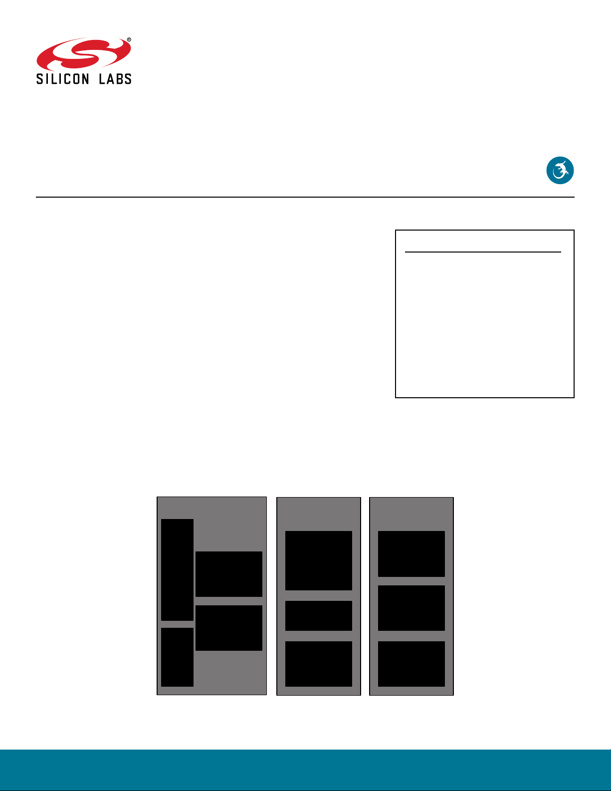
Serial interface
controller
KEY FEATURES
• Bluetooth 5 low energy compliant
• Serial interface with hardware flow control
• GPIO control through command API
• Integrated antenna
• TX power up to 8 dBm
• Encrypted bonding and connectivity
• Integrated DC-DC Converter
• Onboard Bluetooth stack
• Centralized OTA through mobile app
library
RadioBluetooth
RX/TX and flow
Command
parser
control
Raw data
Bluetooth 5
compliant
stack
Timers
Radio
transceiver
Chip
antenna
stream
buffers
GPIO
OTA
control
silabs.com | Building a more connected world. Rev. 1.2
manager
Matching
network
Page 2

1. Ordering Information
BGX13P Bluetooth ® Xpress Module Data Sheet
Ordering Information
Table 1.1. Ordering Information
Bluetooth
Protocol
Ordering Code
BGX13P22GA-V31R Bluetooth Low
BGX13P22GA-V31 Bluetooth Low
BGX13P22GA-V21R Bluetooth Low
BGX13P22GA-V21 Bluetooth Low
The maximum TX power allowed by different regional certification authorities may differ from the maximum TX power the module can
produce. End-product manufacturers must verify that the module is configured to meet regulatory limits for each region in accordance
with the formal certification test reports.
Stack
Energy
Energy
Energy
Energy
Xpress firmware version
1.2.2045.0 2.4 GHz @ 8 dBm Built-in 8 Reel
1.2.2045.0 2.4 GHz @ 8 dBm Built-in 8 Tray
1.0.927.2 2.4 GHz @ 8 dBm Built-in 8 Reel
1.0.927.2 2.4 GHz @ 8 dBm Built-in 8 Tray
Frequency Band
@ Max TX Power Antenna GPIO Packaging
silabs.com | Building a more connected world. Rev. 1.2 | 2
Page 3

Table of Contents
1. Ordering Information ............................2
2. Electrical Specifications ...........................5
2.1 Electrical Characteristics ..........................5
2.1.1 Absolute Maximum Ratings ........................5
2.1.2 Operating Conditions ..........................5
2.1.3 Power Consumption...........................6
2.1.4 2.4 GHz RF Transceiver Characteristics ....................7
2.1.5 Non-Volatile Configuration Storage......................8
2.1.6 General-Purpose I/O (GPIO) ........................9
3. Typical Connection Diagrams ........................10
3.1 Typical BGX13P Connections .........................10
4. Layout Guidelines ............................11
4.1 Module Placement and Application PCB Layout Guidelines ...............11
4.2 Effect of Plastic and Metal Materials .......................12
4.3 Locating the Module Close to Human Body ....................12
4.4 2D Radiation Pattern Plots ..........................13
5. Hardware Design Guidelines ........................15
5.1 Power Supply Requirements .........................15
5.2 Reset Functions .............................15
5.3 Debug and Firmware Updates .........................15
6. Pin Definitions ..............................16
6.1 BGX13P Device Pinout ...........................16
7. Functional overview ............................18
7.1 Introduction ...............................18
7.2 Communication Use Cases..........................18
7.3 Embedded Interface ............................18
7.4 Command Mode and Streaming Mode ......................18
7.5 Command API ..............................19
7.6 GPIO Control ..............................19
7.7 Device Configuration ............................19
7.8 Security Features .............................19
7.9 OTA .................................19
7.10 Direct Test Mode Support ..........................19
8. Package Specifications ..........................20
8.1 Package Outline .............................20
8.2 Recommended PCB Land Pattern .......................21
silabs.com
| Building a more connected world. Rev. 1.2 | 3
Page 4

8.3 Package Marking .............................22
9. Soldering Recommendations ........................23
9.1 Soldering Recommendations .........................23
10. Certifications ..............................24
10.1 Bluetooth ...............................24
10.2 CE .................................24
10.3 FCC .................................24
10.4 ISED Canada ..............................25
10.5 Japan ................................27
10.6 KC South Korea .............................27
10.7 NCC Taiwan ..............................28
11. Revision History............................. 29
silabs.com | Building a more connected world. Rev. 1.2 | 4
Page 5

BGX13P
Bluetooth ® Xpress Module Data Sheet
Electrical Specifications
2. Electrical Specifications
2.1 Electrical Characteristics
All electrical parameters in all tables are specified under the following conditions, unless stated otherwise:
• Typical values are based on T
• Radio performance numbers are measured in conducted mode, based on Silicon Laboratories reference designs using output power-specific external RF impedance-matching networks for interfacing to a 50 Ω antenna.
• Minimum and maximum values represent the worst conditions across supply voltage, process variation, and operating temperature,
unless stated otherwise.
The BGX13P module has only one external supply pin (VDD). There are several internal supply rails mentioned in the electrical specifications, whose connections vary based on transmit power configuration. Refer to for the relationship between the module's external
VDD pin and internal voltage supply rails.
Refer to for more details about operational supply and temperature limits.
2.1.1 Absolute Maximum Ratings
Stresses above those listed below may cause permanent damage to the device. This is a stress rating only, and functional operation of
the devices at those or any other conditions above those indicated in the operation listings of this specification is not implied. Exposure
to maximum rating conditions for extended periods may affect device reliability. For more information on the available quality and reliability data, see the Quality and Reliability Monitor Report at http://www.silabs.com/support/quality/pages/default.aspx.
= 25°C and VDD = 3.3 V, by production test and/or technology characterization.
AMB
Table 2.1. Absolute Maximum Ratings
Parameter Symbol Test Condition Min Typ Max Unit
Storage temperature range T
Voltage on any supply pin V
Voltage ramp rate on any
STG
DDMAX
V
DDRAMPMAX
-40 — 85 °C
-0.3 — 3.8 V
— — 1 V / µs
supply pin
DC voltage on any GPIO pin V
Maximum RF level at input P
Total current into supply pins I
Total current into VSS
DIGPIN
RFMAX2G4
VDDMAX
I
VSSMAX
Source — — 200 mA
Sink — — 200 mA
-0.3 — VDD+0.3 V
— — 10 dBm
ground lines
Current per I/O pin I
IOMAX
Sink — — 50 mA
Source — — 50 mA
Current for all I/O pins I
IOALLMAX
Sink — — 200 mA
Source — — 200 mA
Junction temperature T
J
-40 — 105 °C
2.1.2 Operating Conditions
The following subsections define the operating conditions for the module.
silabs.com | Building a more connected world. Rev. 1.2 | 5
Page 6

BGX13P Bluetooth ® Xpress Module Data Sheet
Electrical Specifications
2.1.2.1 General Operating Conditions
Table 2.2. General Operating Conditions
Parameter Symbol Test Condition Min Typ Max Unit
Operating ambient tempera-
T
A
-40 25 85 °C
ture range
VDD operating supply volt-
V
VDD
2.4 3.3 3.8 V
age
2.1.3 Power Consumption
Unless otherwise indicated, typical conditions are: VDD = 3.3 V. T = 25 °C. Minimum and maximum values in this table represent the
worst conditions across process variation at T = 25 °C.
Table 2.3. Power Consumption
Parameter Symbol Test Condition Min Typ Max Unit
Active supply current, Unconnected, Idle
Active supply current, Advertising
I
ACTIVE_IDLE
I
ACTIVE_ADV
Baud rate ≤ 9600 bps — 3 — µA
Baud rate > 9600 bps — 3.25 — mA
Interval = 546.25 ms, Baud rate ≤
— 90 — µA
9600 bps
Interval = 20 ms, Baud rate ≤
— 2 — mA
9600 bps
Interval = 546.25 ms, Baud rate >
— 3.3 — mA
9600 bps
Active supply current, Connected, 15 ms Interval
Supply current in low power
mode
I
ACTIVE_CONN
I
LPM
Interval = 20 ms, Baud rate >
— 4.7 — mA
9600 bps
Idle, Baud Rate ≤ 9600 bps — 660 — µA
TX/RX (acknowledged) at highest
— 3.5 — mA
throughput, Baud Rate ≤ 9600
bps
TX/RX (unacknowledged) at high-
— 4 — mA
est throughput, Baud Rate ≤ 9600
bps
Idle, Baud Rate > 9600 bps — 3.5 — mA
TX/RX (acknowledged) at highest
— 5.25 — mA
throughput, Baud Rate > 9600
bps
TX/RX (unacknowledged) at high-
— 7 — mA
est throughput, Baud Rate > 9600
bps
Radio disabled — 3 — µA
Radio enabled, Advertising, Inter-
— 90 — µA
val = 546.25 ms
Radio enabled, Advertising, Inter-
— 2 — mA
val = 20 ms
silabs.com | Building a more connected world. Rev. 1.2 | 6
Page 7
BGX13P Bluetooth ® Xpress Module Data Sheet
Electrical Specifications
2.1.4 2.4 GHz RF Transceiver Characteristics
2.1.4.1 RF Transmitter General Characteristics for 2.4 GHz Band
Unless otherwise indicated, typical conditions are: T = 25 °C, VDD = 3.3 V. DC-DC on. Crystal frequency = 38.4 MHz. RF center frequency 2.45 GHz. Conducted measurement from the antenna feedpoint.
Table 2.4. RF Transmitter General Characteristics for 2.4 GHz Band
Parameter Symbol Test Condition Min Typ Max Unit
Maximum TX power
1
POUT
MAX
— 8 — dBm
Minimum active TX Power POUT
Output power step size POUT
Output power variation vs
supply at POUT
MAX
Output power variation vs
temperature at POUT
MAX
Output power variation vs RF
frequency at POUT
MAX
RF tuning frequency range F
POUT
POUT
POUT
RANGE
MIN
STEP
VAR_V
VAR_T
VAR_F
CW -27 — dBm
-5 dBm< Output power < 0 dBm — 0.5 — dB
0 dBm < output power <
POUT
MAX
2.4 V < V
< 3.3 V — 0.05 — dB
VDD
— 0.5 — dB
From -40 to +85 °C — 1.7 — dB
Over RF tuning frequency range — 0.3 — dB
2400 — 2483.5 MHz
Note:
1. Supported transmit power levels are determined by the ordering part number (OPN). Transmit power ratings for all devices covered in this datasheet can be found in the Max TX Power column of the Ordering Information Table.
2.1.4.2 RF Receiver General Characteristics for 2.4 GHz Band
Unless otherwise indicated, typical conditions are: T = 25 °C, VDD = 3.3 V. DC-DC on. Crystal frequency = 38.4 MHz. RF center frequency 2.45 GHz. Conducted measurement from the antenna feedpoint.
Table 2.5. RF Receiver General Characteristics for 2.4 GHz Band
Parameter Symbol Test Condition Min Typ Max Unit
RF tuning frequency range F
Receive mode maximum
spurious emission
Max spurious emissions during active receive mode, per
FCC Part 15.109(a)
RANGE
SPUR
SPUR
RX
RX_FCC
30 MHz to 1 GHz — -57 — dBm
1 GHz to 12 GHz — -47 — dBm
216 MHz to 960 MHz, Conducted
Measurement
Above 960 MHz, Conducted
2400 — 2483.5 MHz
— -55.2 — dBm
— -47.2 — dBm
Measurement
silabs.com | Building a more connected world. Rev. 1.2 | 7
Page 8
BGX13P Bluetooth ® Xpress Module Data Sheet
Electrical Specifications
2.1.4.3 RF Receiver Characteristics for Bluetooth Low Energy in the 2.4GHz Band, 1 Mbps Data Rate
Unless otherwise indicated, typical conditions are: T = 25 °C, VDD = 3.3 V. DC-DC on. Crystal frequency = 38.4 MHz. RF center frequency 2.45 GHz. Conducted measurement from the antenna feedpoint.
Table 2.6. RF Receiver Characteristics for Bluetooth Low Energy in the 2.4GHz Band, 1 Mbps Data Rate
Parameter Symbol Test Condition Min Typ Max Unit
Sensitivity, 0.1% BER SENS
Signal is reference signal1. Using
— -94.8 — dBm
DC-DC converter.
With non-ideal signals as speci-
— -94.4 — dBm
fied in RF-PHY.TS.4.2.2, section
4.6.1.
Note:
1. Reference signal is defined 2GFSK at -67 dBm, Modulation index = 0.5, BT = 0.5, Bit rate = 1 Mbps, desired data = PRBS9;
interferer data = PRBS15; frequency accuracy better than 1 ppm.
2.1.4.4 RF Receiver Characteristics for Bluetooth Low Energy in the 2.4GHz Band, 2 Mbps Data Rate
Unless otherwise indicated, typical conditions are: T = 25 °C, VDD = 3.3 V. DC-DC on. Crystal frequency = 38.4 MHz. RF center frequency 2.45 GHz. Conducted measurement from the antenna feedpoint.
Table 2.7. RF Receiver Characteristics for Bluetooth Low Energy in the 2.4GHz Band, 2 Mbps Data Rate
Parameter Symbol Test Condition Min Typ Max Unit
Sensitivity, 0.1% BER SENS
Signal is reference signal1. Using
— -91.2 — dBm
DC-DC converter.
With non-ideal signals as speci-
— -91.1 — dBm
fied in RF-PHY.TS.4.2.2, section
4.6.1.
Note:
1. Reference signal is defined 2GFSK at -67 dBm, Modulation index = 0.5, BT = 0.5, Bit rate = 2 Mbps, desired data = PRBS9;
interferer data = PRBS15; frequency accuracy better than 1 ppm.
2.1.5 Non-Volatile Configuration Storage
Table 2.8. Non-Volatile Configuration Storage
Parameter Symbol Test Condition Min Typ Max Unit
Update cycles before failure UC 10000 — — cycles
Data retention RET 10 — — years
Supply voltage during update V
DD
2.4 — 3.6 V
silabs.com | Building a more connected world. Rev. 1.2 | 8
Page 9

BGX13P Bluetooth ® Xpress Module Data Sheet
Electrical Specifications
2.1.6 General-Purpose I/O (GPIO)
Table 2.9. General-Purpose I/O (GPIO)
Parameter Symbol Test Condition Min Typ Max Unit
Input low voltage V
Input high voltage V
Output high voltage relative
to VDD
Output low voltage relative to
VDD
IL
IH
V
OH
GPIO pins — — VDD*0.3 V
GPIO pins VDD*0.7 — — V
Sourcing 3 mA, VDD ≥ 3 V,
VDD*0.8 — — V
Drive Strength = Weak
Sourcing 1.2 mA, VDD ≥ 1.62 V,
VDD*0.6 — — V
Drive Strength = Weak
Sourcing 20 mA, VDD ≥ 3 V,
VDD*0.8 — — V
Drive Strength = Strong
Sourcing 8 mA, VDD ≥ 1.62 V,
VDD*0.6 — — V
Drive Strength = Strong
V
OL
Sinking 3 mA, VDD ≥ 3 V,
— — VDD*0.2 V
Drive Strength = Weak
Sinking 1.2 mA, VDD ≥ 1.62 V,
— — VDD*0.4 V
Drive Strength = Weak
Sinking 20 mA, VDD ≥ 3 V,
— — VDD*0.2 V
Drive Strength = Strong
Input leakage current I
I/O pin pull-up/pull-down resistor
Pulse width of pulses removed by the glitch suppression filter
Output fall time, From 70%
to 30% of V
DD
Output rise time, From 30%
to 70% of V
DD
IOLEAK
R
PUD
t
IOGLITCH
t
IOOF
t
IOOR
Sinking 8 mA, VDD ≥ 1.62 V,
— — VDD*0.4 V
Drive Strength = Strong
All GPIO pins, GPIO ≤ VDD — 0.1 30 nA
30 40 65 kΩ
15 25 45 ns
CL = 50 pF,
— 1.8 — ns
Drive Strength = Strong
CL = 50 pF,
— 4.5 — ns
Drive Strength = Weak
CL = 50 pF,
— 2.2 — ns
Drive Strength = Strong
CL = 50 pF,
— 7.4 — ns
Drive Strength = Weak
silabs.com | Building a more connected world. Rev. 1.2 | 9
Page 10
BGX13P Bluetooth ® Xpress Module Data Sheet
Typical Connection Diagrams
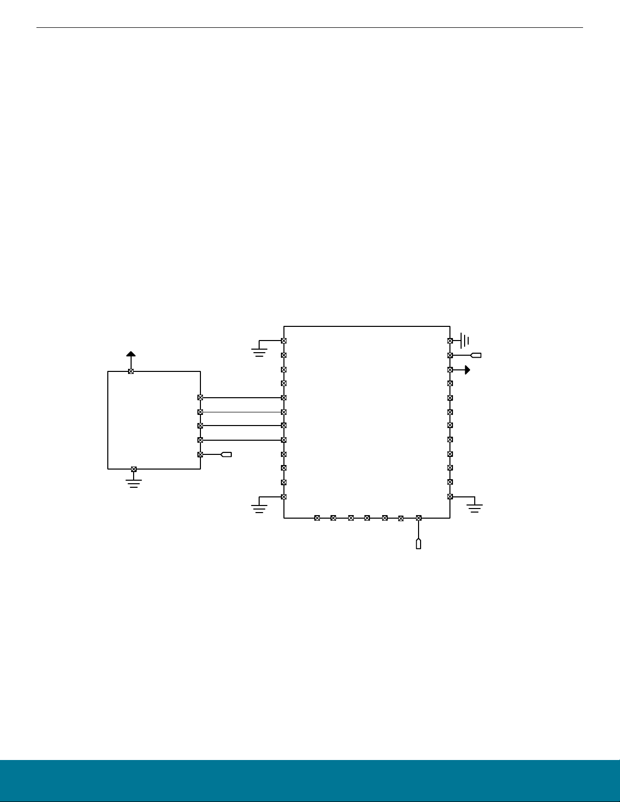
3. Typical Connection Diagrams
3.1 Typical BGX13P Connections
Typical connections for the BGX13P module are shown in Figure 3.1 Typical Connections for BGX13P on page 10. This diagram
shows connections for:
• Power supplies
• Reset line
Note:
It is recommended to connect the RESETn line to an open-drain IO pin on the host CPU.
• UART connection to an embedded host
• Optional BOOT pin connection - BOOT is an active-low digital input that will force the module into a DFU bootloader state after device reset. BOOT can be tied to IOVDD or left disconnected if it is unused.
+3.3 V
Host CPU
VSS
RTS
CTS
GPIO
GND
GPIO0
GPIO1
GPIO2
RX
TX
RESETn
UART_TX
UART_RX
UART_CTS
UART_RTS
GPIO3
GPIO4
DNC
GND
DNC
GPIO5
BGX13P
GPIO6
GPIO7
DNC
DNC
BOOT
RESETn
BOOT
GND
VDD
DNC
DNC
DNC
DNC
DNC
GND
RESETn
+3.3 V
NC
NC
NC
Figure 3.1. Typical Connections for BGX13P
silabs.com | Building a more connected world. Rev. 1.2 | 10
Page 11
BGX13P Bluetooth ® Xpress Module Data Sheet
Layout Guidelines
4. Layout Guidelines
For optimal performance of the BGX13P (with integrated antenna), please follow the PCB layout guidelines and ground plane recommendations indicated in this section.
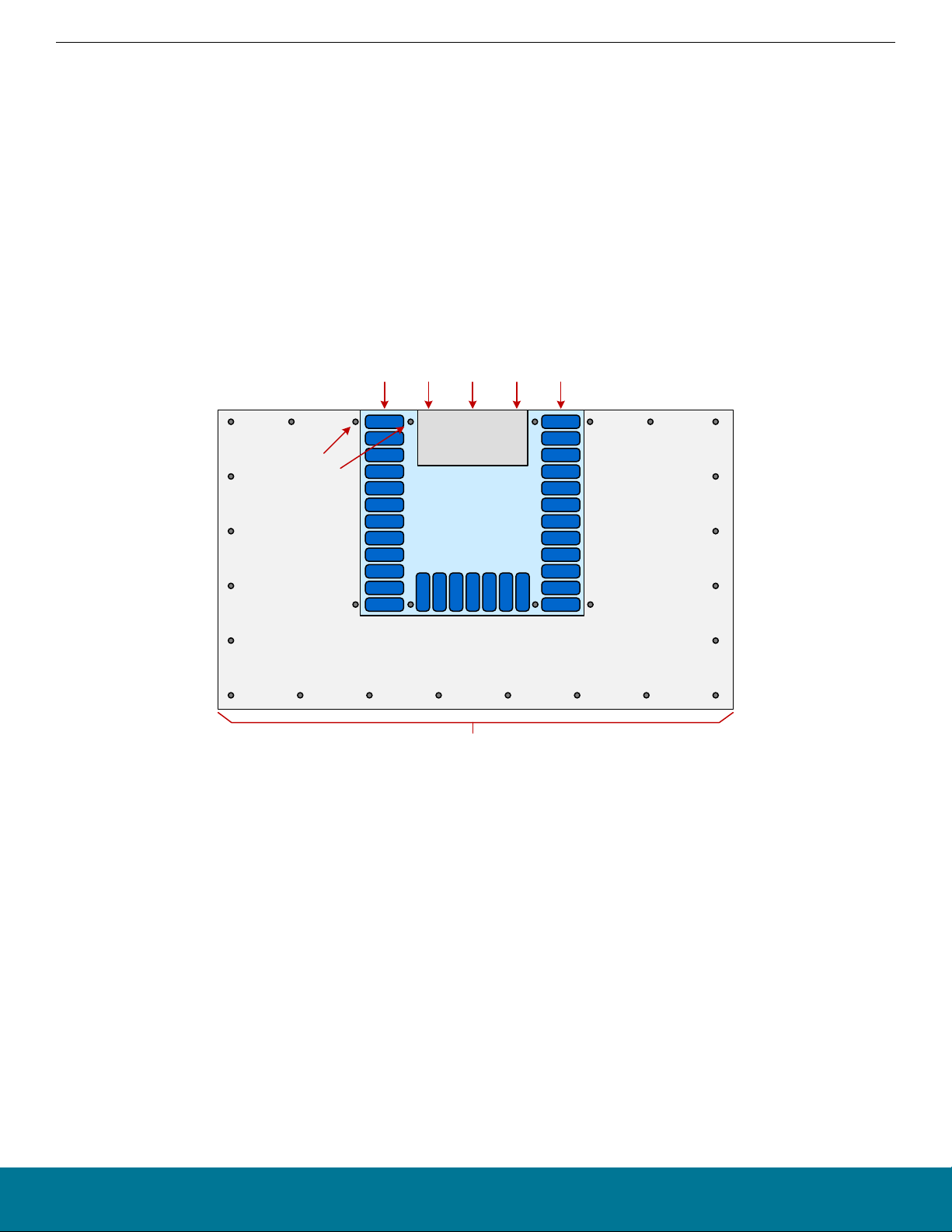
4.1 Module Placement and Application PCB Layout Guidelines
• Place the module at the edge of the PCB, as shown in Figure 4.1 Recommended Application PCB Layout for BGX13P with Integra-
ted Antenna on page 11.
• Do not place any metal (traces, components, battery, etc.) within the clearance area of the antenna.
• Connect all ground pads directly to a solid ground plane.
• Place the ground vias as close to the ground pads as possible.
• Do not place plastic or any other dielectric material in contact with the antenna.
Align module edge with PCB edge
Place vias close to
each of the
module’s GND pads
GND
GND
Antenna Clearance
No metal in this area
Wireless Module
(Top View)
Place vias along all PCB edges
GND
GND
Figure 4.1. Recommended Application PCB Layout for BGX13P with Integrated Antenna
silabs.com | Building a more connected world. Rev. 1.2 | 11
Page 12

BGX13P
Bluetooth ® Xpress Module Data Sheet
Layout Guidelines
Figure 4.2 Non-optimal Module Placements for BGX13P with Integrated Antenna on page 12 shows examples of layouts that will re-
sult in severely degraded RF performance.
Figure 4.2. Non-optimal Module Placements for BGX13P with Integrated Antenna
The amount of ground plane surrounding the sides of the module will also impact the maximum RF range, as shown in Figure
4.3 Impact of GND Plane Size vs. Range for BGX13P on page 12.
Figure 4.3. Impact of GND Plane Size vs. Range for BGX13P
4.2 Effect of Plastic and Metal Materials
Do not place plastic or any other dielectric material in close proximity to the antenna.
Any metallic objects in close proximity to the antenna will prevent the antenna from radiating freely. The minimum recommended distance of metallic and/or conductive objects is 10 mm in any direction from the antenna except in the directions of the application PCB
ground planes.
4.3 Locating the Module Close to Human Body
Placing the module in contact with or very close to the human body will negatively impact antenna efficiency and reduce range.
silabs.com | Building a more connected world. Rev. 1.2 | 12
Page 13

4.4 2D Radiation Pattern Plots
BGX13P Bluetooth ® Xpress Module Data Sheet
Layout Guidelines
Figure 4.4. Typical 2D Radiation Pattern – Front View
Figure 4.5. Typical 2D Radiation Pattern – Side View
silabs.com | Building a more connected world. Rev. 1.2 | 13
Page 14

BGX13P Bluetooth ® Xpress Module Data Sheet
Layout Guidelines
Figure 4.6. Typical 2D Radiation Pattern – Top View
silabs.com | Building a more connected world. Rev. 1.2 | 14
Page 15

BGX13P Bluetooth ® Xpress Module Data Sheet
Hardware Design Guidelines
5. Hardware Design Guidelines
The BGX13P is an easy-to-use module with regard to hardware application design. The additional guidelines in this section should be
followed to guarantee optimal performance.
5.1 Power Supply Requirements
Coin cell batteries cannot withstand high peak currents (e.g. higher than 15 mA). If the peak current exceeds 15 mA, the recommendation is to place a 47 - 100 µF capacitor in parallel with the coin cell battery to improve battery life time. Note that the total current consumption of the application is a combination of the radio, peripherals, and MCU current consumption, and all power consumers must be
taken into account. BGX13P should be powered by a unipolar supply voltage with nominal value of 3.3 V.
5.2 Reset Functions
The BGX13P can be reset by three different methods: by pulling the RESET line low, by the internal watchdog timer, or by software
command. The reset state in BGX13P does not provide any power saving functionality and is not recommended as a means to conserve power. BGX13P has an internal system power-up reset function. The RESET pin includes an on-chip pull-up resistor and can be
left unconnected if no external reset switch or source is used.
5.3 Debug and Firmware Updates
This section contains information on debugging and firmware update methods. For additional information, refer to Section 7.9 OTA
describing firmware update behavior.
silabs.com | Building a more connected world. Rev. 1.2 | 15
Page 16
6. Pin Definitions
6.1 BGX13P Device Pinout
BGX13P Bluetooth ® Xpress Module Data Sheet
Pin Definitions
GND
GPIO0
GPIO1
GPIO2
UART_TX
UART_RX
UART_CTS
UART_RTS
GPIO3
GPIO4
NC
GND
10
11
12
1
2
3
4
5
6
7
8
9
13
14
15
NC
GPIO5
GPIO6
16
GPIO7
17
NC
18
NC
31
30
29
28
27
26
25
24
23
22
21
19
20
BOOT
GND
RESET
VDD
NC
NC
NC
NC
NC
NC
NC
NC
GND
Figure 6.1. BGX13P Device Pinout
The following table provides package pin connections and general descriptions of pin functionality.
For GPIOx configuration information, please see the BGX13 command API documentation.
Table 6.1. BGX13P Device Pinout
Pin Name Pin(s) Description
GND 1, 12, 20, 31 Ground
GPIO0 2 Pin with input/output functionality configured through the command API.
GPIO1 3 Pin with input/output functionality configured through the command API.
GPIO2 4 Pin with input/output functionality configured through the command API.
GPIO3 9 Pin with input/output functionality configured through the command API.
GPIO4 10 Pin with input/output functionality configured through the command API.
GPIO5 14 Pin with input/output functionality configured through the command API.
GPIO6 15 Pin with input/output functionality configured through the command API.
GPI07 16 Pin with input/output functionality configured through the command API.
UART_TX 5 Digital output
silabs.com | Building a more connected world. Rev. 1.2 | 16
Page 17

Pin Name Pin(s) Description
UART_RX 6 Digital input
UART_CTS 7 Digital input
UART_RTS 8 Digital output
Reset input, active low. To apply an external reset source to this pin, it is required
RESETn 30
to only drive this pin low during reset, and let the internal pull-up ensure that reset
is released.
VDD 29 Module Power Supply.
BGX13P Bluetooth ® Xpress Module Data Sheet
Pin Definitions
BOOT 19
Active-low digital input to force module entrance into DFU bootloader state upon
device reset. See command API documentation for functional details.
11,
13,
17,
18,
21,
N/C
22,
23,
No Connect.
24,
25,
26,
27,
28
Note: Pins labeled N/C (No Connect) and any unused GPIO pins should be left disconnected. UART flow control pins may also be left
disconnected when feature is unused.
silabs.com | Building a more connected world. Rev. 1.2 | 17
Page 18

BGX13P
Bluetooth ® Xpress Module Data Sheet
Functional overview
7. Functional overview
7.1 Introduction
The BGX13P creates a Bluetooth 5.0 compliant Bluetooth Low Energy cable replacement interface, facilitating a Bluetooth Low Energy
link to a second embedded device or a mobile device. An embedded MCU controls the device and communicates across the Bluetooth
Low Energy link through a serial interface and control signals. Parameters stored in non-volatile memory and configurable through the
serial interface adjust performance characteristics of the device. Silicon Labs offers iOS and Android mobile libraries for Bluetooth
Xpress devices to speed mobile development and simplify communication with the device. This library also controls OTA management,
facilitating secure and reliable updates to the device’s embedded stack.
This functional overview does not cover each command supported by the command API. The complete command API specification is
available at https://docs.silabs.com/bgx/latest/.
7.2 Communication Use Cases
The BGX13P family facilitates two types of Bluetooth Low Energy communication links:
• BGX-to-mobile
• BGX-to-BGX
In the BGX-to-mobile communication use case, the BGX13P operates as a peripheral that is discoverable and connectable when configured to that state through either the command API or the pin states driven by the embedded MCU. Using the Xpress mobile library,
mobile applications can scan for BGX13P devices, connect, and communicate with the device in both streaming and remote command
modes, where the mobile app can execute command API functions remotely.
In the BGX-to-BGX communication use case, one BGX13P must be configured as the central device and one or more other BGX devices should be configured as a peripheral. Devices can be configured at runtime through the command API, or those settings can be
saved to non-volatile memory so that each device wakes from power-on or low power states as either a peripheral or central. For more
information on advertising and connection options, please see the command API documentation.
7.3 Embedded Interface
The BGX13P family uses an 8-N-1 USART interface for data and flow control signaling. The interface is used both for a raw data
streaming interface and a command interface, depending on additional hardware pin configuration.
UART_TX and UART_RX are defined with flow directions relative to the BGX. Bytes sent from the embedded host to the BGX use the
UART_RX pin. Bytes sent from the BGX to the embedded host appear on the UART_TX pin.
UART_CTS is a digital input that controls the state of the UART_RTS digital output on the other end of the wireless link. Assertion of a
CTS/RTS pair signals that the embedded MCU driving its respective UART_CTS is available to receive bytes.
The baud rate of the BGX13P is a configurable parameter. For information on the process by which a baud rate change gets processed
and executed by the device, please see the command API documentation.
State control signals and visual indicators described below can be assigned to any of the GPIO pins through the command API. These
settings can be stored in non-volatile memory and take effect during the next power cycle. For information on configuration of standard
GPIO and available special function I/O available on the device, please see the command API documentation.
7.4 Command Mode and Streaming Mode
The BGX13P is designed to wake and offer optimized serial interface with hardware flow control. Hardware flow control signaling is
disabled by default. When operating in a peripheral role and when flow control signals are monitored, the device may never need to
leave streaming mode during operation.
However, when use cases require more advanced runtime configuration, the device can switch to command interface through pin or
escape sequence. Commands defined here can control scanning, advertising, connection state, and GPIO settings.
The command interface is also used to configure and store customizable parameters.
Streaming mode can be switched to command mode through an escape sequence of characters if the sequence has been previously
saved in the device's configuration. A command can be issued in command mode to switch to streaming mode. Stream mode and command mode entrance can be controlled through a device port pin state, if a pin has been previously defined for that purpose.
silabs.com | Building a more connected world. Rev. 1.2 | 18
Page 19

BGX13P
Bluetooth ® Xpress Module Data Sheet
Functional overview
7.5 Command API
Each command begins with a command name followed by arguments, and the syntax of each command is defined in the command API
documentation.
The command interface saves settings as key-value pairs. These values can be used at runtime to modify the operational state, and
they can also be stored in non-volatile memory. Values stored in non-volatile memory function to configure the device's startup/default
state.
7.6 GPIO Control
The BGX13P offers 8 GPIO pins. These pins can be configured as state control pins or visual indicator pins. Alternatively, they can be
used as general purpose I/O pins. Digital output settings can be set and digital input state can be read through the command interface
locally or remotely through the remote command execution using the mobile libraries.
7.7 Device Configuration
Device configuration is handled through the command API, where commands are executed when the serial interface is set to operate in
command mode. These commands can also be executed remotely through the mobile library unless prohibited through previous configuration.
Additionally, a device configuration can be generated and saved using Simplicity Studio's Xpress Configurator tool. A generated configuration can be submitted to Silicon Labs through the process defined in that application. Silicon Labs will then validate the configuration
request, generate a custom orderable part number, and deliver first article samples for testing. Developers should contact sales representatives for more information about this process. Once first article samples have been validated by the customer, this custom orderable part number can be ordered directly from Silicon Labs.
7.8 Security Features
BGX13P devices communicate with LE secure connections, establishing encrypted communication upon connection.
Device OTA requires an encrypted image signed by Silicon Laboratories. Only firmware developed, signed, and encrypted by Silicon
Labs can be bootloaded successfully on the device.
7.9 OTA
The BGX13P supports secure OTA of the embedded stack and the command interface. Images are encrypted and signed by Silicon
Laboratories. OTA can be performed through the mobile library APIs. Specific device firmware versions can be selected and programmed through these APIs. See command API documentation for more information.
For information on new functionality including firmware updates to BGX13P, please see https://docs.silabs.com/bgx/latest/. BGX13P
module OPN firmware will not be updated to include newly released features available through OTA and DFU updates provided by
Silicon Labs. Module OPN firmware will only be updated at manufacturing time to provide security-related enhancements.
Contact Silicon Labs technical support for information on customer factory programming options for custom OPN ordering with a specified device firmware version and for customer factory programming options.
7.10 Direct Test Mode Support
The BGX13P's command API offers a command set that configures the device to support the Direct Test Mode (DTM) protocol as defined in the Bluetooth Core Specification Version 4.2, Volume 6, part F.
See the command API for information about commands to support specific DTM test procedures.
silabs.com | Building a more connected world. Rev. 1.2 | 19
Page 20

8. Package Specifications
8.1 Package Outline
BGX13P Bluetooth ® Xpress Module Data Sheet
Package Specifications
Figure 8.1. BGX13P - Top and Side View
Figure 8.2. BGX13P - Bottom View
silabs.com | Building a more connected world. Rev. 1.2 | 20
Page 21
BGX13P Bluetooth ® Xpress Module Data Sheet
Package Specifications
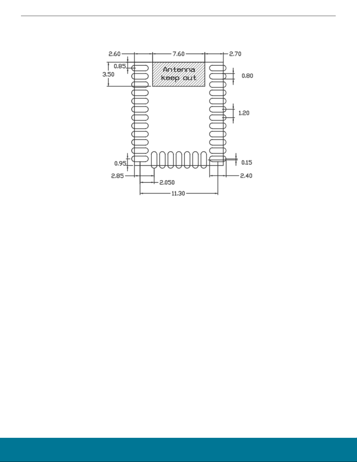
8.2 Recommended PCB Land Pattern
The figure below shows the recommended land pattern. The antenna clearance section is not required for BGX13P module versions
with a U.FL connector.
Figure 8.3. BGX13P Recommended PCB Land Pattern
silabs.com | Building a more connected world. Rev. 1.2 | 21
Page 22

8.3 Package Marking
The figure below shows the module markings printed on the RF-shield.
BGX13P22GAV31
Model: BGX13P22GA
Certification
Marks
BGX13P
Bluetooth ® Xpress Module Data Sheet
Package Specifications
YYWWTTTTTT
Figure 8.4. BGX13P Package Marking
Mark Description
The package marking consists of:
• BGX13Pxxxxxxx - Part number designation.
• Model: BGX13Pxxxx – Model number designation.
• QR Code: YYWWMMABCDE
• YY - Last two digits of the assembly year.
• WW - Two-digit workweek when the device was assembled.
• MMABCDE - Silicon Labs unit code.
• YYWWTTTTTT
• YY – Last two digits of the assembly year.
• WW – Two-digit workweek when the device was assembled.
• TTTTTT – Manufacturing trace code. The first letter is the device revision.
• Certification marks such as the CE logo, FCC and IC IDs, etc. will be engraved on the grayed out area, according to regulatory body
requirements.
silabs.com | Building a more connected world. Rev. 1.2 | 22
Page 23

BGX13P Bluetooth ® Xpress Module Data Sheet
Soldering Recommendations
9. Soldering Recommendations
9.1 Soldering Recommendations
This section describes the soldering recommendations for the BGX13P module.
BGX13P is compatible with industrial-standard reflow profile for Pb-free solders. The reflow profile used is dependent on the thermal
mass of the entire populated PCB, heat transfer efficiency of the oven, and particular type of solder paste used.
• Refer to technical documentations of particular solder paste for profile configurations.
• Avoid using more than two reflow cycles.
• A no-clean, type-3 solder paste is recommended.
• A stainless steel, laser-cut, and electro-polished stencil with trapezoidal walls should be used to assure good solder paste release.
• Recommended stencil thickness is 0.100 mm (4 mils).
• Refer to the recommended PCB land pattern for an example stencil aperture size.
• For further recommendation, please refer to the JEDEC/IPC J-STD-020, IPC-SM-782 and IPC 7351 guidelines.
silabs.com | Building a more connected world. Rev. 1.2 | 23
Page 24

BGX13P
Bluetooth ® Xpress Module Data Sheet
Certifications
10. Certifications
10.1 Bluetooth
The BGX13P is pre-qualified as a Low Energy RF-PHY tested component, having Declaration ID of D037287 and QDID of 101562. For
the qualification of an end product embedding the BGX13P, the above should be combined with the most up to date Wireless Gecko
Link Layer and Host components.
10.2 CE
The BGX13P22 module is in conformity with the essential requirements and other relevant requirements of the Radio Equipment Directive (RED) (2014/53/EU). Please note that every application using the BGX13P22 will need to perform the radio EMC tests on the end
product, according to EN 301 489-17. It is ultimately the responsibility of the manufacturer to ensure the compliance of the end-product.
The specific product assembly may have an impact to RF radiated characteristics, and manufacturers should carefully consider RF
radiated testing with the end-product assembly. A formal DoC is available via www.silabs.com
10.3 FCC
This device complies with Part 15 of the FCC Rules. Operation is subject to the following two conditions:
1. This device may not cause harmful interference, and
2. This device must accept any interference received, including interference that may cause undesirable operation.
Any changes or modifications not expressly approved by Silicon Labs could void the user’s authority to operate the equipment.
FCC RF Radiation Exposure Statement:
This equipment complies with FCC radiation exposure limits set forth for an uncontrolled environment. End users must follow the specific operating instructions for satisfying RF exposure compliance. This transmitter meets both portable and mobile limits as demonstrated
in the RF Exposure Analysis. This transmitter must not be co-located or operating in conjunction with any other antenna or transmitter
except in accordance with FCC multi-transmitter product procedures.
OEM Responsibilities to comply with FCC Regulations:
OEM integrator is responsible for testing their end-product for any additional compliance requirements required with this module installed (for example, digital device emissions, PC peripheral requirements, etc.).
• With BGX13P22 the antenna(s) must be installed such that a minimum separation distance of 9 mm is maintained between the radiator (antenna) and all persons at all times.
• The transmitter module must not be co-located or operating in conjunction with any other antenna or transmitter except in accordance with FCC multi-transmitter product procedures.
Important Note:
In the event that the above conditions cannot be met (for certain configurations or co-location with another transmitter), then the FCC
authorization is no longer considered valid and the FCC ID cannot be used on the final product. In these circumstances, the OEM integrator will be responsible for re-evaluating the end product (including the transmitter) and obtaining a separate FCC authorization.
End Product Labeling
The variants of BGX13P Modules are labeled with their own FCC ID. If the FCC ID is not visible when the module is installed inside
another device, then the outside of the device into which the module is installed must also display a label referring to the enclosed
module. In that case, the final end product must be labeled in a visible area with the following:
"Contains Transmitter Module FCC ID: QOQBGM13P"
Or
"Contains FCC ID: QOQBGM13P"
The OEM integrator has to be aware not to provide information to the end user regarding how to install or remove this RF module or
change RF related parameters in the user manual of the end product.
silabs.com | Building a more connected world. Rev. 1.2 | 24
Page 25

BGX13P
Bluetooth ® Xpress Module Data Sheet
Certifications
10.4 ISED Canada
ISEDC
This radio transmitter (IC: 5123A-BGM13P) has been approved by Industry Canada to operate with the antenna types listed above, with
the maximum permissible gain indicared. Antenna types not included in this list, having a gain greater than the maximum gain indicated
for that type, are strictly prohibited for use with this device.
This device complies with Industry Canada’s license-exempt RSS standards. Operation is subject to the following two conditions:
1. This device may not cause interference; and
2. This device must accept any interference, including interference that may cause undesired operation of the device
RF Exposure Statement
Exception from routine SAR evaluation limits are given in RSS-102 Issue 5.
The models BGM13P32A and BGM13P32E meet the given requirements when the minimum separation distance to human body is 40
mm.
The models BGX13P22GA meet the given requirements when the minimum separation distance to human body is 20 mm.
RF exposure or SAR evaluation is not required when the separation distance is same or more than stated above. If the separation distance is less than stated above the OEM integrator is responsible for evaluating the SAR.
OEM Responsibilities to comply with IC Regulations
The BGX13P modules have been certified for integration into products only by OEM integrators under the following conditions:
• The antenna(s) must be installed such that a minimum separation distance as stated above is maintained between the radiator (antenna) and all persons at all times.
• The transmitter module must not be co-located or operating in conjunction with any other antenna or transmitter.
As long as the two conditions above are met, further transmitter testing will not be required. However, the OEM integrator is still responsible for testing their end-product for any additional compliance requirements required with this module installed (for example, digital
device emissions, PC peripheral requirements, etc.).
IMPORTANT NOTE
In the event that these conditions cannot be met (for certain configurations or co-location with another transmitter), then the ISEDC
authorization is no longer considered valid and the IC ID cannot be used on the final product. In these circumstances, the OEM integrator will be responsible for re-evaluating the end product (including the transmitter) and obtaining a separate ISEDC authorization.
End Product Labeling
The BGX13P module is labeled with its own IC ID. If the IC ID is not visible when the module is installed inside another device, then the
outside of the device into which the module is installed must also display a label referring to the enclosed module. In that case, the final
end product must be labeled in a visible area with the following:
“Contains Transmitter Module IC: 5123A-BGM13P ”
or
“Contains IC: 5123A-BGM13P”
The OEM integrator has to be aware not to provide information to the end user regarding how to install or remove this RF module or
change RF related parameters in the user manual of the end product.
silabs.com | Building a more connected world. Rev. 1.2 | 25
Page 26

BGX13P
Bluetooth ® Xpress Module Data Sheet
Certifications
ISEDC (Français)
Industrie Canada a approuvé l’utilisation de cet émetteur radio (IC: 5123A-BGM13P) en conjonction avec des antennes de type dipolaire à 2.14dBi ou des antennes embarquées, intégrée au produit. L’utilisation de tout autre type d’antenne avec ce composant est proscrite.
Ce composant est conforme aux normes RSS, exonérées de licence d'Industrie Canada. Son mode de fonctionnement est soumis aux
deux conditions suivantes:
1. Ce composant ne doit pas générer d’interférences.
2. Ce composant doit pouvoir est soumis à tout type de perturbation y compris celle pouvant nuire à son bon fonctionnement.
Déclaration d'exposition RF
L'exception tirée des limites courantes d'évaluation SAR est donnée dans le document RSS-102 Issue 5.
Les modules BGM13P32A and BGM13P32E répondent aux exigences requises lorsque la distance minimale de séparation avec le
corps humain est de 40 mm.
Les modules BGX13P22GA répondent aux exigences requises lorsque la distance minimale de séparation avec le corps humain est de
20 mm.
La déclaration d’exposition RF ou l'évaluation SAR n'est pas nécessaire lorsque la distance de séparation est identique ou supérieure à
celle indiquée ci-dessus. Si la distance de séparation est inférieure à celle mentionnées plus haut, il incombe à l'intégrateur OEM de
procédé à une évaluation SAR.
Responsabilités des OEM pour une mise en conformité avec le Règlement du Circuit Intégré
Le module BGX13P a été approuvé pour l'intégration dans des produits finaux exclusivement réalisés par des OEM sous les conditions
suivantes:
• L'antenne (s) doit être installée de sorte qu'une distance de séparation minimale indiquée ci-dessus soit maintenue entre le radiateur
(antenne) et toutes les personnes avoisinante, ce à tout moment.
• Le module émetteur ne doit pas être localisé ou fonctionner avec une autre antenne ou un autre transmetteur que celle indiquée
plus haut.
Tant que les deux conditions ci-dessus sont respectées, il n’est pas nécessaire de tester ce transmetteur de façon plus poussée. Cependant, il incombe à l’intégrateur OEM de s’assurer de la bonne conformité du produit fini avec les autres normes auxquelles il pourrait être soumis de fait de l’utilisation de ce module (par exemple, les émissions des périphériques numériques, les exigences de périphériques PC, etc.).
REMARQUE IMPORTANTE
ans le cas où ces conditions ne peuvent être satisfaites (pour certaines configurations ou co-implantation avec un autre émetteur), l'autorisation ISEDC n'est plus considérée comme valide et le numéro d’identification ID IC ne peut pas être apposé sur le produit final.
Dans ces circonstances, l'intégrateur OEM sera responsable de la réévaluation du produit final (y compris le transmetteur) et de l'obtention d'une autorisation ISEDC distincte.
Étiquetage des produits finis
Les modules BGX13P sont étiquetés avec leur propre ID IC. Si l'ID IC n'est pas visible lorsque le module est intégré au sein d'un autre
produit, cet autre produit dans lequel le module est installé devra porter une étiquette faisant apparaitre les référence du module intégré. Dans un tel cas, sur le produit final doit se trouver une étiquette aisément lisible sur laquelle figurent les informations suivantes:
“Contient le module transmetteur: 5123A-BGM13P ”
or
“Contient le circuit: 5123A-BGM13P”
L'intégrateur OEM doit être conscient qu’il ne doit pas fournir, dans le manuel d’utilisation, d'informations relatives à la façon d'installer
ou de d’enlever ce module RF ainsi que sur la procédure à suivre pour modifier les paramètres liés à la radio.
silabs.com | Building a more connected world. Rev. 1.2 | 26
Page 27
BGX13P
Bluetooth ® Xpress Module Data Sheet
Certifications
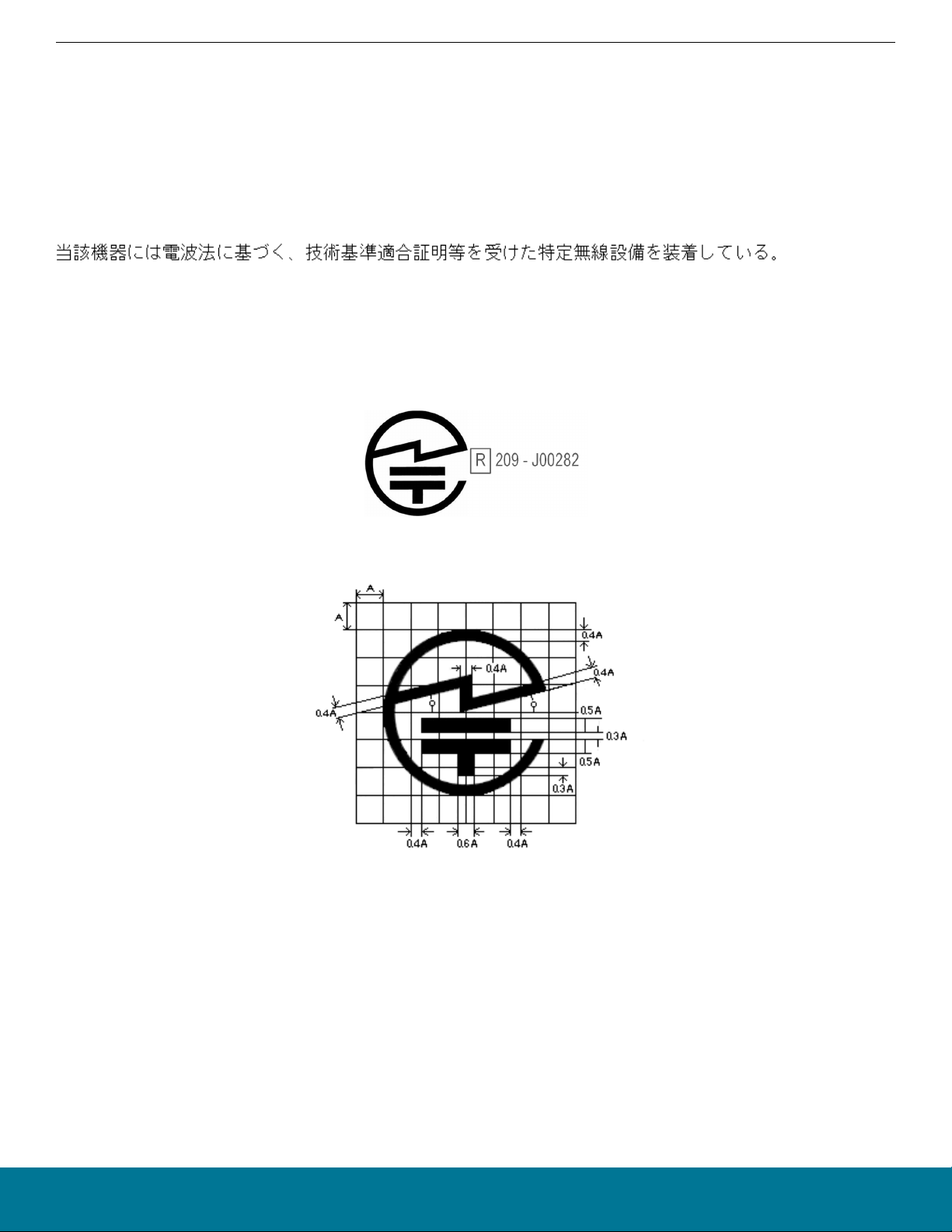
10.5 Japan
The BGM13P22A and BGM13P22E are certified in Japan with certification number 209-J00282.
Since September 1, 2014 it is allowed (and highly recommended) that a manufacturer who integrates a radio module in their host
equipment can place the certification mark and certification number (the same marking/number as depicted on the label of the radio
module) on the outside of the host equipment. The certification mark and certification number must be placed close to the text in the
Japanese language which is provided below. This change in the Radio Law has been made in order to enable users of the combination
of host and radio module to verify if they are actually using a radio device which is approved for use in Japan.
Certification Text to be Placed on the Outside Surface of the Host Equipment:
Translation of the text:
“This equipment contains specified radio equipment that has been certified to the Technical Regulation Conformity Certification under
the Radio Law.”
The "Giteki" marking shown in the figures below must be affixed to an easily noticeable section of the specified radio equipment. Note
that additional information may be required if the device is also subject to a telecom approval.
Figure 10.1. GITEKI Mark and ID
10.6 KC South Korea
The BGX13P22GA have certification in South-Korea.
Figure 10.2. GITEKI Mark
Certification number: R-C-BGT-BGM13P22
silabs.com | Building a more connected world. Rev. 1.2 | 27
Page 28

BGX13P Bluetooth ® Xpress Module Data Sheet
Certifications
10.7 NCC Taiwan
The BGX13P22GA are certified in Taiwan. ID: CCAM18LP1262T4.
According to NCC Low Power Radio Wave Radiation Equipment Management Regulations:
Article 12 A low-power RF equipment that has passed the type approval shall not change the frequency, increase the
power or change the characteristics and functions of the original design without permission.
Article 14 The use of low-power RF equipment shall not affect flight safety and interfere with legal communications; if in-
terference is found, it shall be immediately deactivated and improved until no interference is found.
Legal communication in the preceding paragraph refers to radio communications operating in accordance with
the provisions of the Telecommunications Act.
Low-power RF equipment must withstand interference from legitimate communications or radiological, radiated
electrical equipment for industrial, scientific, and medical applications.
silabs.com | Building a more connected world. Rev. 1.2 | 28
Page 29

BGX13P Bluetooth ® Xpress Module Data Sheet
11. Revision History
Revision 1.2
January, 2021
• Updated 1. Ordering Information.
Revision 1.1
June, 2020
• Updated dimensions Figure 8.3 BGX13P Recommended PCB Land Pattern on page 21
• Added note in 6.1 BGX13P Device Pinout to leave unused and no-connect pins disconnected.
• Updated OPN in Table 1.1 Ordering Information on page 2
• Updated Figure 8.4 BGX13P Package Marking on page 22
• Updated 8.1 Package Outline
• Added Figure 8.1 BGX13P - Top and Side View on page 20
• Added Figure 8.2 BGX13P - Bottom View on page 20
• Updated Certifications chapter 10.1 Bluetooth to 10.7 NCC Taiwan
Revision 1.0
Revision History
December, 2018
• 7.9 OTA: Updated firmware update policy.
• 2.1.1 Absolute Maximum Ratings: Corrected storage temperature.
• Table 2.8 Non-Volatile Configuration Storage on page 8: Corrected minimum supply voltage during update.
• Table 2.2 General Operating Conditions on page 6: Changed VOL parameter from "IOVDD" to "VDD".
• 3.1 Typical BGX13P Connections: Updated typical connection description and diagram with additional detail.
• 8.3 Package Marking: Replaced detailed certification marks and text description with Certification Mark area.
Revision 0.5
August, 2018
• Public Release
Revision 0.1
July 2018
• Initial Release.
silabs.com | Building a more connected world. Rev. 1.2 | 29
Page 30

Simplicity Studio
One-click access to MCU and wireless
tools, documentation, software, source
code libraries & more. Available for
Windows, Mac and Linux!
IoT Portfolio
www.silabs.com/IoT
Disclaimer
Silicon Labs intends to provide customers with the latest, accurate, and in-depth documentation of all peripherals and modules available for system and software implementers using or
intending to use the Silicon Labs products. Characterization data, available modules and peripherals, memory sizes and memory addresses refer to each specific device, and “Typical”
parameters provided can and do vary in different applications. Application examples described herein are for illustrative purposes only. Silicon Labs reserves the right to make changes
without further notice to the product information, specifications, and descriptions herein, and does not give warranties as to the accuracy or completeness of the included information.
Without prior notification, Silicon Labs may update product firmware during the manufacturing process for security or reliability reasons. Such changes will not alter the specifications or
the performance of the product. Silicon Labs shall have no liability for the consequences of use of the information supplied in this document. This document does not imply or expressly
grant any license to design or fabricate any integrated circuits. The products are not designed or authorized to be used within any FDA Class III devices, applications for which FDA
premarket approval is required, or Life Support Systems without the specific written consent of Silicon Labs. A “Life Support System” is any product or system intended to support or
sustain life and/or health, which, if it fails, can be reasonably expected to result in significant personal injury or death. Silicon Labs products are not designed or authorized for military
applications. Silicon Labs products shall under no circumstances be used in weapons of mass destruction including (but not limited to) nuclear, biological or chemical weapons, or
missiles capable of delivering such weapons. Silicon Labs disclaims all express and implied warranties and shall not be responsible or liable for any injuries or damages related to use of
a Silicon Labs product in such unauthorized applications.
Trademark Information
Silicon Laboratories Inc.®, Silicon Laboratories®, Silicon Labs®, SiLabs® and the Silicon Labs logo®, Bluegiga®, Bluegiga Logo®, ClockBuilder®, CMEMS®, DSPLL®, EFM®,
EFM32®, EFR, Ember®, Energy Micro, Energy Micro logo and combinations thereof, “the world’s most energy friendly microcontrollers”, Ember®, EZLink®, EZRadio®, EZRadioPRO®,
Gecko®, Gecko OS, Gecko OS Studio, ISOmodem®, Precision32®, ProSLIC®, Simplicity Studio®, SiPHY®, Telegesis, the Telegesis Logo®, USBXpress®, Zentri, the Zentri logo and
Zentri DMS, Z-Wave®, and others are trademarks or registered trademarks of Silicon Labs. ARM, CORTEX, Cortex-M3 and THUMB are trademarks or registered trademarks of ARM
Holdings. Keil is a registered trademark of ARM Limited. Wi-Fi is a registered trademark of the Wi-Fi Alliance. All other products or brand names mentioned herein are trademarks of
their respective holders.
Silicon Laboratories Inc.
400 West Cesar Chavez
Austin, TX 78701
USA
http: //www.silabs.com
SW/HW
ww.silabs.com/simplicity
w
Quality
ww.silabs.com/quality
w
Support & Community
abs.com/community
www.sil
 Loading...