

Page 1
AN515
Si4010 KEY F OB DEVELOPMENT K IT QUICK S TA RT G UIDE
1. Purpose
Thank you for your interest in Silicon Laboratories Si4010 RF SoC transmitter Key fob development kit. This
development kit (4010-DK KF 434) contains everything you need to develop your software with the Si4010
embedded Si8051 MCU. The key features of the development pla tform are as follows:
The 434 MHz key fob development board has five push buttons and one LED output.
The key fob development board has a battery to enable disconnect from the pr og ra m m i ng interfa c e boar d.
Uses Silicon Laboratories Integrated Development Environment (IDE) for software debugging and can also use
any Keil C compiler, assembler, and linker.
Interfaces with Silicon Laboratories USB Debug Adapter or Toolstick.
Contains a socketed key fob development board for burning the OTP NVM memory.
Contains five blank NVM Si4010 chips and key fob demo bo ards without IC for burn ing and testing user code on
an actual key fob PCB.
2. Kit Contents
The kit contains the following items:
Burning Adapter (P/N MSC-BA 4, shown in Figure 1)
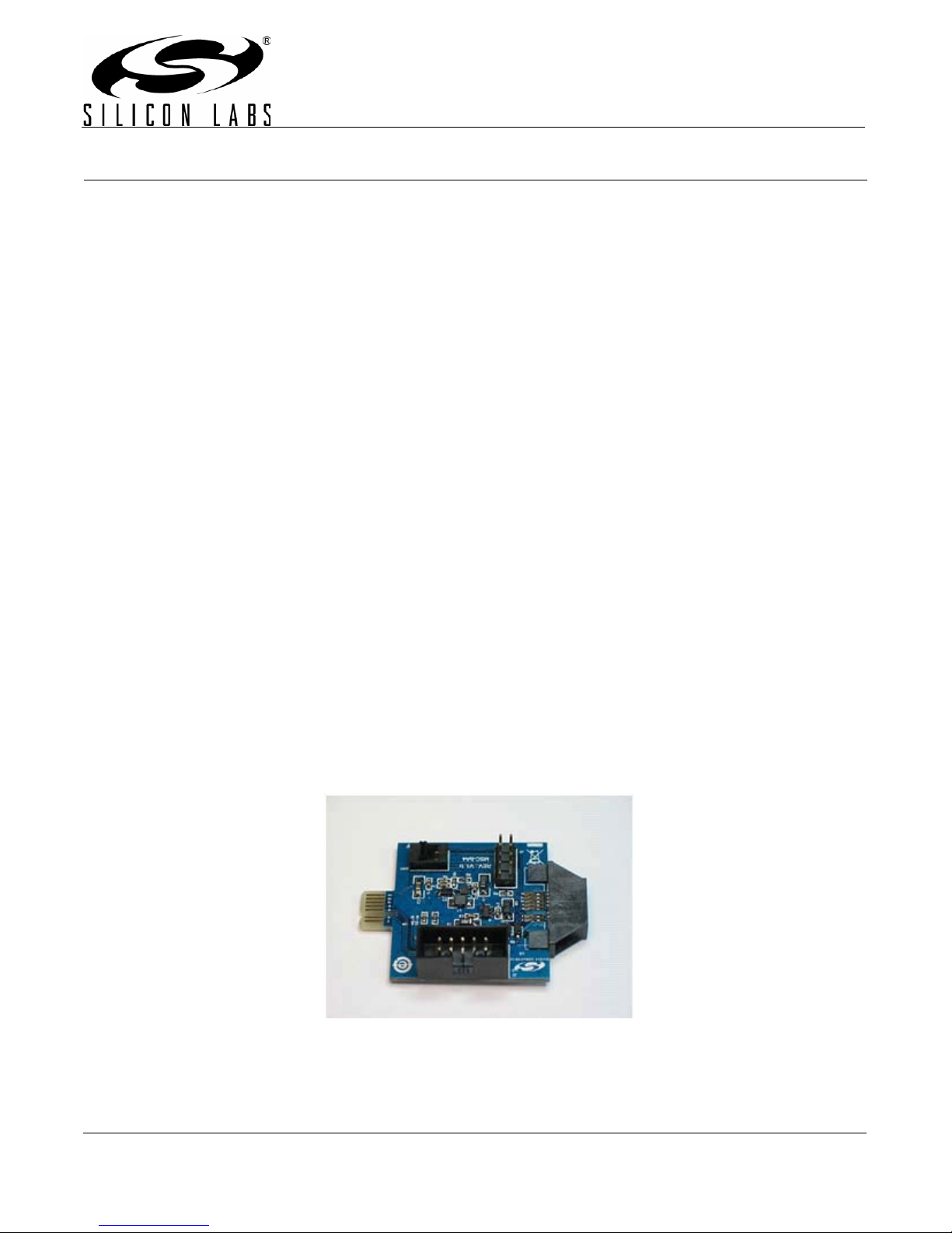
Si4010 Socketed Key fob development board (P/N MSC-DK PE 1, shown in Figure 2)
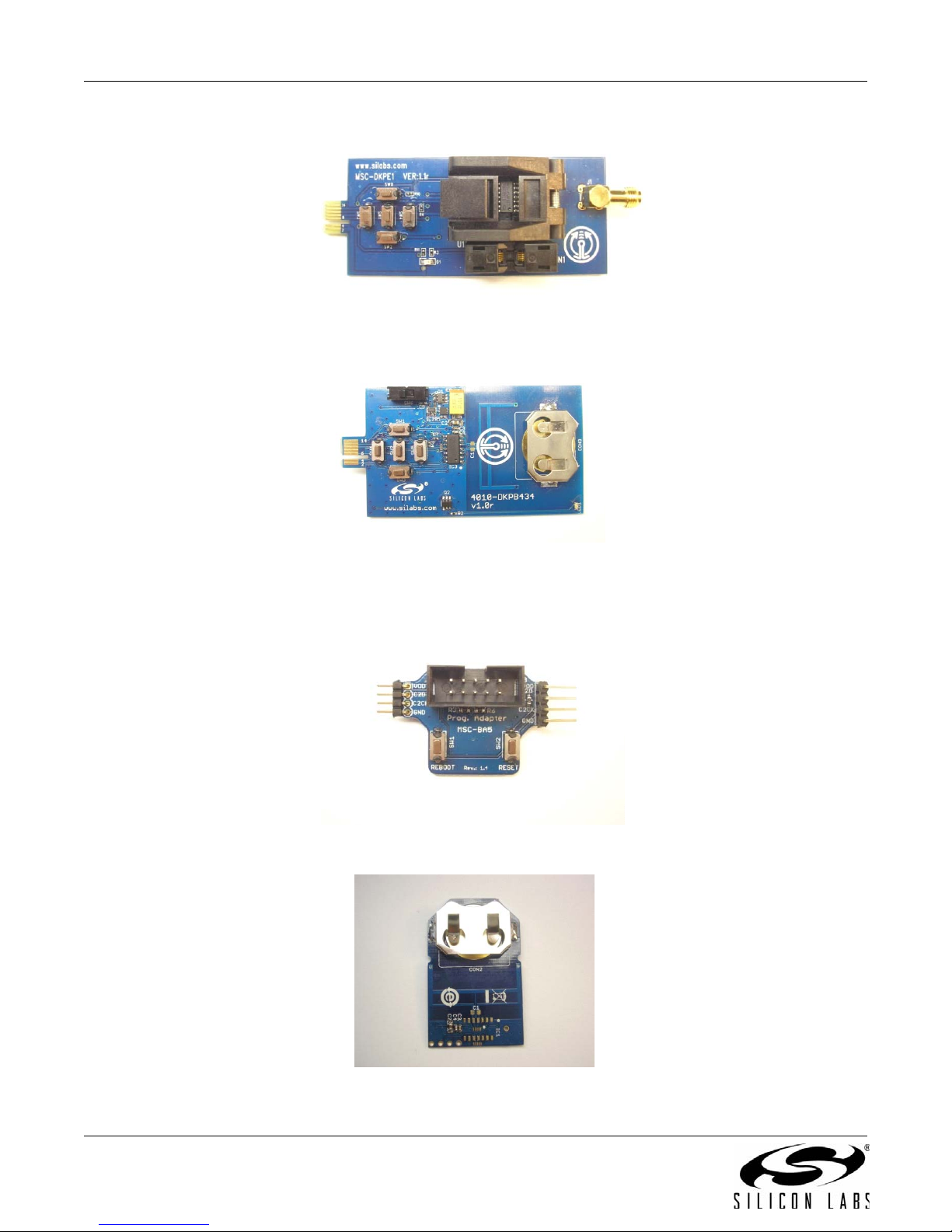
Si4010 SOIC Key Fob development board 434 MHz, PCB ant. (P/N 4010-DK PB 434, shown in Figure 3)
Programming adapter board (P/N MSC-BA 5, shown in Figure 4)
4010 Key fob demo board without IC (quantity = 2) (P/N 4010-UB PB 434, shown in Figure 5)
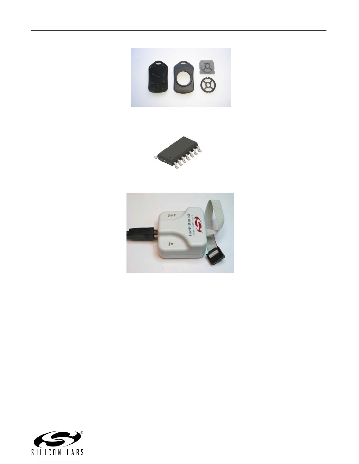
Key fob Plastic Case (translucent grey, P/N MSC-PL PB 1, shown in Figure 6)
WDS CDROM Set (P/N MSC-DKSW1)
Si4010 sample, SOIC Package (rev B1, quantity = 5, P/N Si4010-B1 GS, shown in Figure 7)
USB Cable (P/N MSC-DK CS 5)
EC3 Debug adapter (P/N EC3, shown in Figure 8)
Figure 1. Burning Adapter (P/N MSC-BA 4)
Rev 1.0 7/10 Copyright © 2010 by Silicon Laboratories AN515
Page 2
AN515
Figure 2. Si4010 Socketed Key Fob Development Board (P/N MSC-DK PE 1)
Figure 3. Si4010 SOIC Key Fob Development Board 434 MHz,
PCB Antenna 434 (P/N 4010-DK PB 434)
Figure 4. Programming Adapter Board (P/N MSC-BA 5)
Figure 5. 4010 Key Fob Demo Board without IC (Quantity = 2) (P/N 4010-UB PB 434)
2 Rev 1.0
Page 3
AN515
Figure 6. Key Fob Plastic Case (Translucent Grey) (P/N MSC-PL PB 1)
Figure 7. Si4010 Sample, SOIC Package (Rev B1) (Quantity = 5) (P/N Si4010-B1 GS)
Figure 8. EC3 Debug Adapter (P/N EC3)
Rev 1.0 3
Page 4

AN515
3. Software Installation
The provided software pack contains all the documentation and files needed to develop a user application. It also
contains example applications using API functions and the key fob demo application.
The directory structure is as follows:
+--Si4010 projects
| +--aes_demo
| | +--bin .. Keil uVision and SiLabs IDE files
| | +--out .. output directory for Keil toolchain
| | +--src .. aes_demo source code
| +--common
| | +--lib .. Si4010 additional API functions library
| | +--src .. Si4010 required files
| +--fcast_demo .. frequency casting (tuning) demo
| | +--bin
| | +--out
| | +--src
| +--fstep_demo .. frequency two step tuning demo
| | +--bin
| | +--out
| | +--src
| +--tone_demo .. continuous wave (tone) demo
| | +--bin
| | +--out
| | +--src
| +--keyfob_demo .. simple keyfob demo
| | +--bin
| | +--out
| | +--src
| +--rke_demo .. advanced keyfob demo with AES
| | +--bin
| | +--out
| | +--src
+--Start_here_documentation.. Development kit documents
+--Silabs_IDE .. SiLabs IDE for debugging applications
| +--hlp
| +--IDEfiles
+--NVM_burning_tool .. PC program for burning Si4010 NVM memory
Copy the directory structure in a directory of your choice. The recommended directory is
C:\SiLabs\MCU\Si4010\
Thus, the final directory tree should look like the following:
C:
+--SiLabs
+--MCU
+--Si4010
+--Start_here_documentation
+--Silabs_IDE
+--si4010 projects
+--NVM_burning_tool
4 Rev 1.0
Page 5

AN515
4. Hardware Setup using a USB Debug Adapter
A detailed description about the IDE and debug adapters can be found in the Si4010 Development Kit User's
Guide.
The target board is connected to a PC running the Silicon Laboratories IDE via the USB Debug Adapter as shown
in Figure 9.
Figure 9. Target Board and Debug Adapter
Perform the following steps to set up the debug adapter:
1. Connect the EC3 Debug Adapter to the J2 connector on the Burning Adapter board with the 10- pin ribbon
cable.
2. Connect one end of the USB cable to the USB connector on the USB Debug Adapter.
3. Connect the other end of the USB cable to a USB Port on the PC.
4. Reset the firmware of the Debug adapter by running the following application:
\Silabs_IDE\usb_debug_adapter_firmware_reset.exe
(This operation needs to be done only once per USB Debug Adapter before a new version of the IDE can be
used.)
5. Run Silabs_IDE\ide.exe
The first time the IDE program is run, it will automatically update the correct firmware for the adapter.
Note: Remove power from the target board and the USB Debug Adapter before connecting or disconnecting the ribbon cab le
from the target board. Connecting or disconnecting the cable when the device s have power can damage the device
and/or the USB Debug Adapter.
Rev 1.0 5
Page 6

AN515
5. Silicon Labs IDE Run
To run the IDE, open a *.wsp file e.g. aes_demo\bin\aes_demo.wsp with Silabs_IDE\ide.exe. Then, associate the
*.wsp extension with the Silabs_IDE\ide.exe file. To run the Silicon Labs IDE in general, open the *.wsp project file
or run Silabs_IDE\ide.exe.
6. Keil Toolchain Integration
The project files in examples assume that the Keil too lch ain is installed to: C:\Keil directory. The location of the Keil
toolchain can be easily changed in t he pr oje ct files . An ev alu at i on ve rsion of the Keil toolchain can be downlo aded
from the Keil web site, http://www.keil.com/. This free version has 2 kB code limitation and starts the code at
0x0800 address. The Keil free evaluation version can be unlocked to become a 4k version with no code placement
limitation by following the directions given in application note “AN104: Integrating Keil 8051 Tools into the Silicon
Labs IDE”, which covers Keil toolchain integration and license management. Contact your Silicon Laboratories
sales representative or distributor for application assistance.
7. Known Issues
There is an issue related to the LED driver, which demonstrates itself only under the following circumst ances when
all three conditions are satisfied:
1. The device programming level is Factory or User. For those levels, the C2 debugging interface is enabled after
the boot by a boot routine.
2. The device has been disconnected from the Silicon Labs IDE. “Disconnected” is meant in the software sense
(not physically) using the Connect/Disconnect buttons on IDE, or the device is running the User code
automatically after the boot without ever being connected to the IDE.
3. The device is running a code that turns the LED on and off.
If all the conditions are satisfied, after the first LED blink when the LED is turned off, the GPIO4 stops working and
is no longer visible to the application.
If the device programming level is Run or the C2 debugging interface is internally disabled, there is no issue. The
LED can be turned on and off without affecting the device GPIO4 functionality.
The issue can be summarized as fo llows: Whenever th e C2 debugging interface is enabled and the device is not
connected to the IDE and the LED is turned on and off, then the GPIO4 will stop functioning. Since, in Run mode,
the C2 is disabled after the boot process finishes, the GPIO4 is not affected.
Therefore, this issue only affects the software development process and inconveniences the developer. After the
application is finalized and the chip is programmed as Run, there is no issue.
There are several possible software workarounds; see details in the Si4010 key fob development kit user guide.
6 Rev 1.0
Page 7

NOTES:
AN515
Rev 1.0 7
Page 8

AN515
The information in this document is believed to be accurate in all respects at the time of publication but is subject to change without
notice. Silicon Laboratories assumes no responsibility for errors and omissions, and disclaims responsibility for any consequences
resulting from the use of information included herein. Additionally, Silicon Laboratories assumes no responsibility for the functioning of undescribed features or parameters. Silicon Laboratories reserves the right to make changes without further notice. Silicon
Laboratories makes no warranty, representation or guarantee regarding the suitability of its products for any particular purpose,
nor does Silicon Laboratories assume any liability arising out of the application or use of any product or circuit, and specifically
disclaims any and all liability, including without limitation consequential or incidental damages. Silicon Laboratories products are
not designed, intended, or authorized for use in applications intended to support or sustain life, or for any other application in which
the failure of the Silicon Laboratories product could create a situation where personal injury or death may occur. Should Buyer
purchase or use Silicon Laboratories products for any such unintended or unauthorized application, Buyer shall indemnify and
hold Silicon Laboratories harmless against all claims and damages.
CONTACT INFORMATION
Silicon Laboratories Inc.
Silicon Laboratories Inc.
400 West Cesar Chavez
Austin, TX 78701
Please visit the Silicon Labs Technical Support web page:
https://www.silabs.com/support/pages/contacttechnicalsupport.aspx
and register to submit a technical support request.
Silicon Laboratories and Silicon Labs are trademarks of Silicon Laboratories Inc.
Other products or brandnames mentioned herein are trademarks or registered trademarks of their respective holders
8 Rev 1.0
 Loading...