

Page 1
AN0021: Analog to Digital Converter
(ADC)
This application note describes how to use the Analog to Digital
Converter (ADC) of EFM32 Gecko Series 0 and 1 devices to convert
an analog input voltage to a digital value. Many aspects of
the ADC, including inputs, references, and the different operating
modes are described. Calibration routines for offset and gain are
also included.
The provided software examples show how to use the different operating modes of the
ADC. The example projects are configured for the EFM32 Gecko Series 0 and 1 devices, but can easily be ported to other EZR32 Wireless MCU and EFR32 Wireless
Gecko devices by changing the project settings.
For simplicity, EFM32 Wonder Gecko, Gecko, Giant Gecko, Leopard Gecko, Tiny
Gecko, Zero Gecko, and Happy Gecko are a part of the EFM32 Gecko Series 0.
EZR32 Wonder Gecko, Leopard Gecko, and Happy Gecko are a part of the EZR32
Wireless MCU Series 0.
EFM32 Pearl Gecko and Jade Gecko (and future devices) are a part of the EFM32
Gecko Series 1.
EFR32 Blue Gecko, Flex Gecko, and Mighty Gecko are a part of the EFR32 Wireless
Gecko Series 1.
KEY POINTS
• There are new ADC features in EFM32
Gecko Series 1 devices.
• This document discusses ADC operation
and advanced features.
• The ADC supports offset and gain
calibration.
• This application note includes:
• This PDF document
• Source files
• Example C-code
• Multiple IDE projects
+
ADC
...0101110...
-
silabs.com | Smart. Connected. Energy-friendly. Rev. 1.11
Page 2

AN0021: Analog to Digital Converter (ADC)
Analog to Digital Converter
1. Analog to Digital Converter
1.1 Introduction
The EFM32 Gecko ADC is a Successive Approximation Register (SAR) architecture. The maximum resolution is 12 bits, which can
achieve one million samples per second (Msps). The integrated input MUX can select the ADC input from external pins or internal signals. With PRS and DMA, the ADC can operate without CPU intervention, minimizing current consumption or allowing the core to do
other work. The ADC can be clocked at different speeds and run using different warm-up modes to reduce the energy consumption
even further.
This application note discusses general operation and usage of the ADC. In addition, advanced features and power saving techniques
are described. Software examples of ADC operation both with DMA and PRS are included. Offset and Gain Calibration of the ADC is
also described and included in the software examples.
For extremely low power periodic ADC sampling, a software example that enters Energy Mode 2 (EM2) between each ADC sample is
also included. This is the best way to do low power ADC sampling for sampling frequencies below a couple of kHz.
silabs.com | Smart. Connected. Energy-friendly. Rev. 1.11 | 1
Page 3

1.2 Overview
AN0021: Analog to Digital Converter (ADC)
Analog to Digital Converter
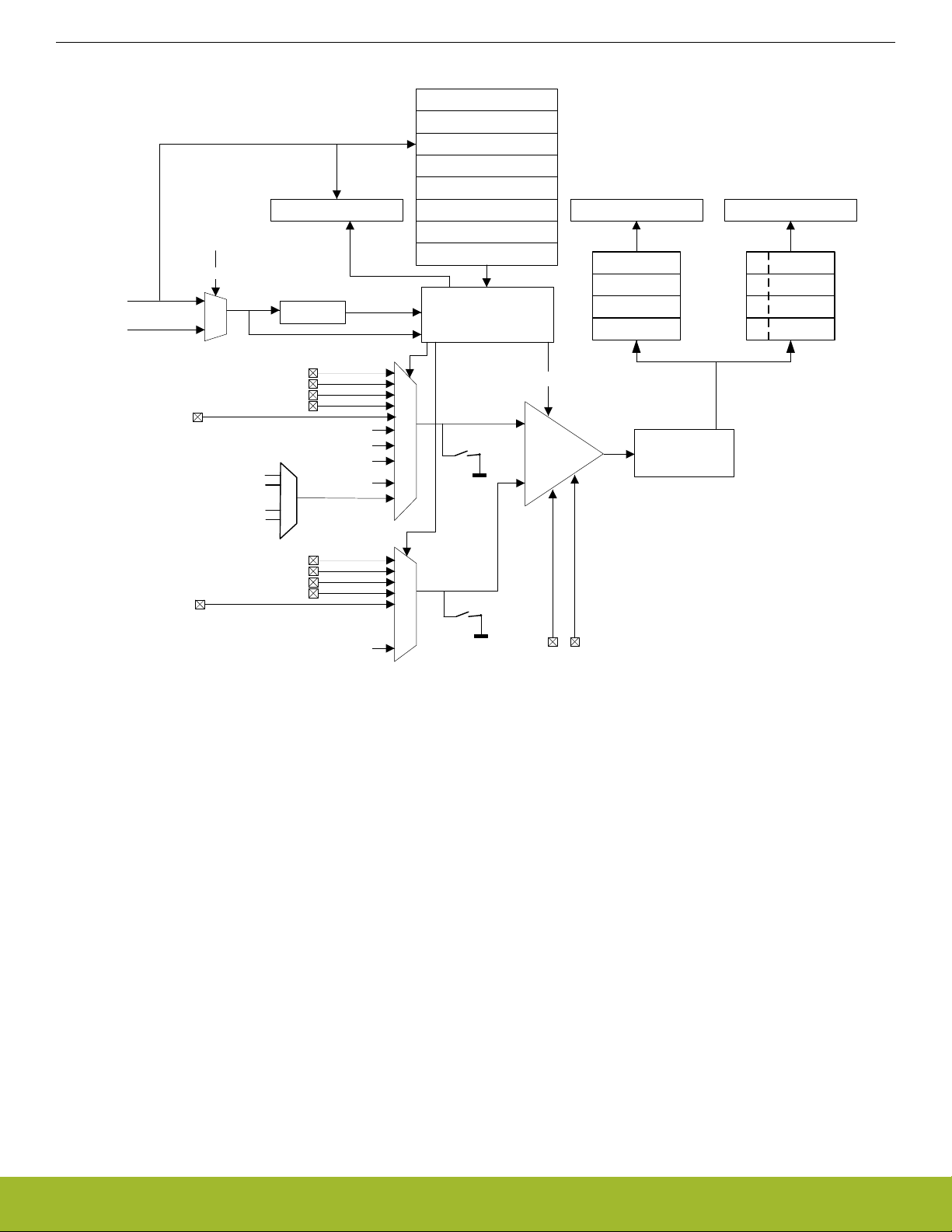
The Figure
1.1 ADC Overview of EFM32 Giant Gecko on page 2 and Figure 1.2 ADC Overview of EFM32 Pearl Gecko on page 3
illustrate the internal connections of the inputs, reference selection, and registers.
ADCn_CTRL
ADCn_CMD
ADCn_SINGLECTRL
ADCn_SCANCTRL
3
Sequencer
+
-
ADCn
ADCn_STATUS
Prescaler
ADCn_CH0
ADCn_CH1
ADCn_CH2
ADCn_CH3
ADCn_CH4
ADCn_CH5
ADCn_CH6
ADCn_CH7
ADC_CLKHFPERCLK
DAC0
DAC1
Temp
V
DD
V
V
V
ref
/
DD
SS
/2
ADCn_SINGLEDATA
ADCn_SCANDATA
Oversampling
filter
Result
buffer
Control
SAR
V
DD
1.25 V
2.5 V
5 V differential
2x(VDD-VSS)
Figure 1.1. ADC Overview of EFM32 Giant Gecko
silabs.com | Smart. Connected. Energy-friendly. Rev. 1.11 | 2
Page 4
HFPERCLK
ASYNCCLK
ADCn
ADCn
ADCCLKMODE
ADC_CLK
ADCn_STATUS
Conversion clock
Prescaler
(adc_clk_sar)
ADC_CLK
ADCn_BIASPROG
ADCn_CMPTHR
ADCn_CTRL
ADCn_CMD
ADCn_SINGLECTRL
ADCn_SINGLECTRLX
ADCn_SCANCTRL
ADCn_SCANCTRLX
Sequencer
AN0021: Analog to Digital Converter (ADC)
Analog to Digital Converter
ADCn_SINGLEDATA ADCn_SCANDATA
SCAN
INPUTID
SINGLESAMPLE
FIFO
SCAN SAMPLE
FIFO
APORT0X
APORT0Y
AVDD
DVDD
DECOUPLE
IOVDD
APORT1X
APORT2X
APORT3X
APORT4X
APORT1Y
APORT2Y
APORT3Y
APORT4Y
DAC0OUT0
DAC0OUT1
vdd_mux
TEMP
VSS
INP_MUX
Control
+
Oversampling
filter
-
INN_MUX
VSS
ADCn_EXTP ADCn_EXTN
Figure 1.2. ADC Overview of EFM32 Pearl Gecko
Some new ADC features (see the list below) are added in the EFM32 Gecko Series 1 and EFR32 Wireless Gecko Series 1 devices.
•
Externally controllable conversion start time using PRS in TIMED mode
• Can be run during EM2 and EM3, waking up the system upon various enabled interrupts
• Can be run during EM2 and EM3 with DMA enabled to pull data from the FIFOs without waking up the system
• Automated clock gating to save power when not converting
• Supports up to 144 external input channels and 11 internal inputs
• Includes temperature sensor and random number generator function
• Programmable scan sequence
• Up to 32 configurable samples in scan sequence
• Four deep FIFOs to store conversion data along with a channel ID and an option to overwrite old data when full
• Programmable watermark (DVL) to generate a SCAN interrupt
• Supports window compare function
• Programmable single-channel conversion
• Four deep FIFOs to store conversion data along with an option to overwrite old data when full
• Programmable watermark (DVL) to generate a SINGLE interrupt
• Supports window compare function
• Programmable and preset input full scale (peak-to-peak) range (VFS) with selectable reference sources
• User-programmable dividers for flexible VFS options from internal, external, or supply voltage reference sources
• Interrupt generation and/or a DMA request when
• Programmable number of converted data available in the single FIFO (also generates DMA request)
silabs.com | Smart. Connected. Energy-friendly. Rev. 1.11 | 3
Page 5

AN0021: Analog to Digital Converter (ADC)
• Programmable number of converted data available in the scan FIFO (also generates DMA request)
Single FIFO overflow or underflow
•
• Scan FIFO overflow or underflow
• Latest Single conversion tripped compare logic
• Latest Scan conversion tripped compare logic
• Analog over-voltage interrupt
• Programming Error interrupt due to APORT Bus Request conflict or NEGSEL programming error
Analog to Digital Converter
silabs.com | Smart. Connected. Energy-friendly. Rev. 1.11 | 4
Page 6

AN0021: Analog to Digital Converter (ADC)
General Operation
2. General Operation
2.1 Clock Selection
The ADC has an internal pre-scaler which can divide the selected ADC conversion clock source. Any factor between 1 and 128 can be
chosen by writing a value between 0 and 127 to the PRESC bit field in the ADCn_CTRL register.
The symbols for different clock sources can be found in Figure 1.1 ADC Overview of EFM32 Giant Gecko on page 2 and Figure
1.2 ADC Overview of EFM32 Pearl Gecko on page 3.
Table 2.1. ADC Clock Selection
Item EFM32 Gecko Series 0 and EZR32
Series 0
ADC peripheral clock source (register in-
HFPERCLK HFPERCLK
EFM32 Gecko Series 1 and EFR32 Wireless
Gecko Series 1
terface)
ADC conversion clock source HFPERCLK The ADC_CLK is selected by ADCCLKMODE bit
field in the ADCn_CTRL register
•
HFPERCLK (ADCCLKMODE = 0)
• ASYNCCLK (ADCCLKMODE = 1)
ASYNCCLK source — Selected by ADC0CLKSEL bit field in the
CMU_ADCCTRL register
•
Disabled (ADC0CLKSEL = 0)
• AUXHFRCO (ADC0CLKSEL = 1)
• HFXO (ADC0CLKSEL = 2)
• HFSRCCLK (ADC0CLKSEL = 3)
ADC conversion clock frequency ADC_CLK = HFPERCLK / (1 to 128)
Range is from 32 kHz to 13 MHz
Clock source for ADC operation in EM2
— AUXHFRCO (ASYNCCLK) is the only available
and EM3
adc_clk_sar = ADC_CLK / (1 to 128)
Range is from 32 kHz to 16 MHz
option during EM2 or EM3
2.2 Input Selection
The
external inputs can either be selected as single-ended inputs or combined to allow for differential inputs (see 3.6 Analog Port
(APORT) for ADC). The DIFF bit field in the ADCn_SINGLECTRL or ADCn_SCANCTRL register enables differential mode.
The ADC input signals are shielded fairly well against other noisy signals within the EFM32 Gecko. If high ADC accuracy is needed, it is
advisable not to use any of the unused ADC input pins for noise-inducing activities, such as serial communication.
2.2.1 Single-Ended Mode
In single-ended mode the input signal is measured with ground as the negative input. The voltage span between 0 V and the selected
reference is divided in small steps according to the selected resolution.
The result is an unsigned number between 0 and 2
resolution
- 1, indicating where the input voltage is located in the span between ground
and the reference voltage.
silabs.com | Smart. Connected. Energy-friendly. Rev. 1.11 | 5
Page 7

AN0021: Analog to Digital Converter (ADC)
General Operation
2.2.2 Differential Mode
differential mode the measured value is the difference between two inputs. Since one input is defined as the positive input and the
In
other is defined as the negative input, the difference can be positive or negative depending on which input is higher. As a result, the
conversion result is a signed number represented in two's complement form. If the negative input is higher than the positive input, the
converted value is negative (see 4.3 Differential Inputs and 5.3 Single and Scan Conversion with Differential Inputs). Note that the ADC
cannot convert negative voltages in reference to ground.
Table 2.2. ADC Input Selection
Item EFM32 Gecko Series 0 and EZR32 Series 0 EFM32 Gecko Series 1 and EFR32 Wireless
Gecko Series 1
External inputs for Single-
Up to 8, fix on pins PD0 – PD7 Up to 144 through APORT
Ended mode
External inputs for Differential
mode
Up to 8, fix on pins PD0 – PD7
•
Two neighboring inputs are used in differential
Up to 72 through APORT
mode, for instance channel 0 and channel 1 is
one differential pair, channel 2 and channel 3
another
• The lowest channel number is the positive differential input
Internal inputs 6 Up to 11
Input filtering Low pass RC filter or an internal decoupling ca-
—
pacitor
Temperature sensor Set INPUTSEL bit field in the ADCn_SIN-
GLECTRL register to TEMP
Offset calibration Set INPUTSEL bit field in the ADCn_SIN-
GLECTRL register to DIFF0 (short between posi-
Set POSSEL bit field in the ADCn_SINGLECTRL
register to TEMP
Set POSSEL and NEGSEL bit fields in the
ADCn_SINGLECTRL register to VSS
tive and negative inputs)
silabs.com | Smart. Connected. Energy-friendly. Rev. 1.11 | 6
Page 8

AN0021: Analog to Digital Converter (ADC)
General Operation
2.3 Reference Selection
convert an analog voltage to a digital value, the ADC needs a reference voltage to which it compares the incoming analog voltage.
To
Since the ADC cannot measure voltages larger than the reference voltage, the reference voltage should be above the maximum expected measured voltage.
The selected reference source is combined with internal circuitry to produce the full-scale voltage (VFS) for the converter. VFS is the
full input range of the converter, from the lowest possible input voltage to the highest. For single-ended conversions, the input range on
the selected positive input is from 0 to VFS. For differential conversions, the input to the converter is the difference between the positive
and negative input selections. The ADC conversion result ranges from -VFS/2 to +VFS/2.
The maximum and minimum input voltage which the ADC can recognize at any external pin is limited to the supply voltages. If VFS is
configured to be larger than the supply range (for example, VFS configured to 5 V when operating on a 3.3 V supply), the full ADC
range is not available.
The ADC cannot measure negative voltages or voltages larger than the reference voltage. As a result, it is important to keep both inputs within the electrical limits of the device.
Table 2.3. ADC Reference Selection
Item EFM32 Gecko Series 0 and EZR32 Series 0 EFM32 Gecko Series 1 and EFR32 Wireless
Gecko Series 1
Internal bandgap reference • 1.25 V
•
2.5 V (supply voltage > 2.5 V)
• 5 V differential (supply voltage > 2.75 V)
Internal reference • VDD
•
Unbuffered 2 x VDD
External single-ended refer-
Pin PD6 as input Use ADCn_EXTP pin as input
ence
External differential reference • Use pin PD6 as positive input
•
Use pin PD7 as negative input
• Reference = 2 x (PD6 – PD7)
GPBIASACC bit field of the
— • Set to 0 (HIGHACC) when an internal bandgap
ADCn_BIASPROG register
• 1.25 V
•
2.5 V
• 5 V differential
• AVDD
• 2 x AVDD
• Use ADCn_EXTP pin as positive input
•
Use ADCn_EXTN pin as negative input
• Reference = 2 x (ADCn_EXTP – ADCn_EXTN)
reference source is used
•
Set to 1 (LOWACC) when AVDD or an external
pin reference is used
silabs.com | Smart. Connected. Energy-friendly. Rev. 1.11 | 7
Page 9

AN0021: Analog to Digital Converter (ADC)
General Operation
2.4 Conversions
conversion consists of acquisition and approximation phases. The input is sampled in the acquisition phase before it is converted to
A
digital representation during the approximation phase. The acquisition time can be configured independently for scan sequence and
single channel conversions by setting AT bit field in the ADCn_SINGLECTRL or ADCn_SCANCTRL register.
The symbols for different clock sources can be found in Figure 1.1 ADC Overview of EFM32 Giant Gecko on page 2 and Figure
1.2 ADC Overview of EFM32 Pearl Gecko on page 3.
Table 2.4. ADC Conversions
Item EFM32 Gecko Series 0 and EZR32 Series 0 EFM32 Gecko Series 1 and EFR32 Wireless
Gecko Series 1
ADC_CLK Pre-scaled HFPERCLK HFPERCLK or ASYNCCLK
adc_clk_sar — Pre-scaled ADC_CLK
Acquisition time (AT) 1 to 256 (integer power of 2) ADC_CLK cycles 1 to 256 (integer power of 2) adc_clk_sar cycles
Minimum acquisition time for
2 µs —
VDD/3
Minimum acquisition time for
the internal temperature sensor
2 µs AT bit field of the ADCn_SINGLECTRL or
ADCn_SCANCTRL register should be set to a
value of 9 (256 adc_clk_sar cycles)
ADC warm-up time Based on HFPERCLK Based on ADC_CLK
ADC total conversion time per
In ADC_CLK cycles
In adc_clk_sar cycles
output
•
Tacq equals the number of
Tconv = (Tacq + N) x OVSRSEL
Tconv = (Tacq + (N + 1)) x OVSRSEL
acquisition cycles
• N is the resolution in bits
• OVSRSEL is the oversampling ratio when oversampling is enabled
2.5 ADC Modes
The ADC contains two separate programmable modes: single channel mode and scan mode. Both modes have separate configuration
and result registers. Both modes may be set up to run only once per trigger or to automatically repeat after each operation. The scan
mode has priority over single channel mode.
silabs.com | Smart. Connected. Energy-friendly. Rev. 1.11 | 8
Page 10

AN0021: Analog to Digital Converter (ADC)
General Operation
2.5.1 Single Channel Mode
single channel mode, the ADC converts one input either one time or continuously if the REP bit field in the ADCn_SINGLECTRL
In
register is set (see 4.1 Single Conversion and 5.1 Single and Scan Conversion). The DIFF bit field in the ADCn_SINGLECTRL register
selects whether differential or single-ended inputs are used.
Table 2.5. ADC Single Channel Mode
Item EFM32 Gecko Series 0 and EZR32 Series 0 EFM32 Gecko Series 1 and EFR32 Wireless
Gecko Series 1
Input selection The input for single conversion is defined by the
bit field INPUTSEL in the ADCn_SINGLECTRL
register
The POSSEL and NEGSEL bit fields in the
ADCn_SINGLECTRL register select the input signals
FIFO for conversion results — 4 x 32 bit
Programmable FIFO watermark (DVL) to generate SINGLE interrupt
— The DVL bit field of the ADCn_SINGLECTRLX
register controls the FIFO watermark crossing
which sets the SINGLEDV bit in the ADCn_STATUS register
SINGLEDV bit in the
ADCn_STATUS register is set
SINGLEOF bit in ADCn_IF register is set
ADCn_SINGLEFIFOCOUNT
Valid data in the ADCn_SINGLEDATA register (DVL+1) number of single channel conversion re-
sults are available in single FIFO
Result is not read before the next result is ready,
the first result is overwritten
Signals that a result from a single channel FIFO
has been overwritten before being read
— Number of unread data available in single FIFO
register
ADCn_SINGLEFIFOCLEAR
— Clear single FIFO content
register
silabs.com | Smart. Connected. Energy-friendly. Rev. 1.11 | 9
Page 11

AN0021: Analog to Digital Converter (ADC)
General Operation
2.5.2 Scan Mode
scan mode, the ADC can be configured to convert a sequence of different inputs, either one time or continuously if the REP bit field
In
in the ADCn_SCANCTRL register is set (see 4.2 Scan Conversion with DMA Transfer and 5.1 Single and Scan Conversion). The DIFF
bit field in the ADCn_SCANCTRL register selects whether differential or single-ended inputs are used. DMA can be used to transfer
results to RAM after each conversion. All the results can then be read from RAM after the sequence has finished.
Table 2.6. ADC Scan Mode
Item EFM32 Gecko Series 0 and EZR32 Series 0 EFM32 Gecko Series 1 and EFR32 Wire-
less Gecko Series 1
Input selection The inputs included in the scan sequence are
defined by the bit field INPUTMASK in
ADCn_SCANCTRL register
The inputs included in the scan sequence
are defined by the ADCn_SCANMASK,
ADCn_SCANINPUTSEL and
ADCn_SCANNEGSEL registers
FIFO for conversion results — 4 x 32 bit
Programmable FIFO watermark (DVL)
to generate SCAN interrupt
— The DVL field of the ADCn_SCANCTRLX
register controls the FIFO watermark crossing which sets the SCANDV bit in the
ADCn_STATUS register
SCANDV bit in the ADCn_STATUS
register is set
SCANOF bit in ADCn_IF register is
set
Valid data in the ADCn_SCANDATA register (DVL+1) number of scan conversion results
are available in scan FIFO
Result is not read before the next result is ready,
the first result is overwritten
Signals that a result from a scan FIFO has
been overwritten before being read
ADCn_SCANDATAX register — The FIFO data is tagged with SCANINPU-
TID and can be read along with the scan
data using this register
ADCn_SCANFIFOCOUNT register — Number of unread data available in scan
FIFO
ADCn_SCANFIFOCLEAR register — Clear scan FIFO content
silabs.com | Smart. Connected. Energy-friendly. Rev. 1.11 | 10
Page 12

AN0021: Analog to Digital Converter (ADC)
General Operation
2.6 Warm-Up Modes
power-on, the ADC requires some time for internal bias currents and references to settle prior to starting a conversion. This time
After
period is called the warm-up time and is performed by hardware. Firmware must program the number of clock cycles required to count
at least 1 µs in the TIMEBASE bit field of the ADCn_CTRL register.
Normally, the ADC is warmed up only when samples are requested and is shut off when there are no more samples waiting. However,
if lower latency is needed, configuring the WARMUPMODE bit field in the ADCn_CTRL allows the ADC and/or reference to stay warm
between samples, reducing the warm-up time or eliminating it altogether. Note that keeping the ADC and/or reference enabled between
samples increases the energy consumption of the ADC.
Note: Only the reference selected for scan mode is kept warm. To avoid warm-up time in single conversion mode, the single conversion reference needs to be the same as the scan conversion reference.
Table 2.7. ADC Warm-up Mode of EFM32 Gecko Series 0
Warmup Mode EFM32 Gecko Series 0 and EZR32 Series 0
NORMAL • ADC and references are shut off when there are no samples waiting
•
When entering Energy Mode 2 or 3, the ADC must be stopped and WARMUPMODE must be set
to NORMAL
• Total time = Bandgap reference warm-up time (5 µs) + ADC warm-up time (1 µs) + ADC conversion time
FASTBG • Bandgap warm-up is eliminated, but with reduced reference accuracy
•
Total time = ADC warm-up time (1 µs) + ADC conversion time
KEEPSCANREFWARM • The reference selected for scan mode is kept warm. The ADC will still need to be warmed up
before conversion
Total time = ADC warm-up time (1 µs) + ADC conversion time
•
KEEPADCWARM • The ADC and the reference selected for scan mode are kept warm
Total time = ADC conversion time
•
Table 2.8. ADC Warm-up Mode of EFM32 Gecko Series 1
Warmup Mode EFM32 Gecko Series 0 and EZR32 Series 1
NORMAL • ADC and references are shut off when there are no samples waiting
Total time = ADC warm-up time (5 µs) + ADC conversion time
•
KEEPINSTANDBY • The reference selected for scan mode is kept warm, but the ADC is powered down
The ADC will initiate a 1 us warm-up period before a conversion begins
•
• Total time = ADC warm-up time (1 µs) + ADC conversion time
KEEPINSLOWACC • It is similar to KEEPINSTANDBY, but continuously tracks the input, keeping the input multiplexer
connected to the analog bus
•
Total time = ADC warm-up time (1 µs) + ADC conversion time
KEEPADCWARM • The ADC and the reference selected for scan mode are kept warm
Total time = ADC conversion time
•
silabs.com | Smart. Connected. Energy-friendly. Rev. 1.11 | 11
Page 13

AN0021: Analog to Digital Converter (ADC)
Advanced Features
3. Advanced Features
3.1 Bias Current Programming
The current consumption of the ADC can be adjusted through the ADCn_BIASPROG register. Adjusting this bitfield also affects the
performance and bandwidth of the ADC. The default register values should be used to ensure correct operation of the ADC within the
specified clock speed range and with all configurations. The bias current settings should only be changed while the ADC is disabled
(i.e., in NORMAL warm-up mode and no conversion in progress).
Table 3.1. ADC Bias Current Programming
Item EFM32 Gecko Series 0 and EZR32 Series 0 EFM32 Gecko Series 1 and EFR32 Wireless
Gecko Series 1
BIASPROG and HALFBIAS
bit fields of the ADCn_BIASPROG register
COMPBIAS bit field of the
ADCn_BIASPROG register
ADCBIASPROG bit field of
the ADCn_BIASPROG register
Scale the bias current of the bandgap reference —
Scale the bias current of the ADC comparator —
— • Scale the internal bias of the ADC
•
For proper operation, the ADC conversion
speed must be scaled accordingly
silabs.com | Smart. Connected. Energy-friendly. Rev. 1.11 | 12
Page 14

AN0021: Analog to Digital Converter (ADC)
Advanced Features
3.2 Oversampling
higher than 12-bit accuracy is needed, the ADC can automatically sample and average the result in hardware. The number of sam-
If
ples for each averaged result can be selected as 2n for n = [1..12]. If oversampling is enabled, the ADC result is not ready until all the
samples are converted and averaged (see 4.4 Oversampling and 5.2 Single and Scan Conversion with Oversampling).
The result is averaged by accumulating samples and right shifting the result. For 2x, 4x, 8x and 16x oversampling the result is not right
shifted. Instead, the result consists of more than 12 bits. See Table 3.2 Oversampling Result Shifting and Resolution on page 13 for
oversampling result representation.
Table 3.2. Oversampling Result Shifting and Resolution
Oversampling Setting Number of Right Shifts Result Resolution (# bits)
2x 0 13
4x 0 14
8x 0 15
16x 0 16
32x 1 16
64x 2 16
128x 3 16
256x 4 16
512x 5 16
1024x 6 16
2048x 7 16
4096x 8 16
If the samples of the measured signal are affected by uncorrelated random noise added to each sample, oversampling and averaging
be used to increase the signal-to-noise ratio. The number of additional samples needed to get n additional bits of meaningful data
can
in the result is given by the following equation.
Note: samples = 2
2n
Note that an accurate result requires more time to sample the signal. For example, this equation can be used to get a 16 bit accuracy at
the expense of using more time per sample because the signal must be sampled many times. To get 4 additional bits of meaningful
data for the 12-bit ADC in the EFM32 Gecko, the number of samples needed equals 2
2*4
which is 256 samples.
3.3 Peripheral Reflex System
The ADC can be configured as both a consumer and a producer of PRS signals. Both scan and single conversions can be triggered by
a PRS signal and PRS signals can also be produced when a conversion is finished.
Often the ADC samples a voltage with fixed intervals and, preferably, without the CPU intervention. Periodic measurements can be
achieved by using the Peripheral Reflex System and a timer (producer) that runs continuously and sends a PRS pulse to the ADC (consumer) with specific intervals. When the ADC receives a PRS pulse, it triggers a conversion start. A conversion-finished interrupt can
then handle the result (see 4.5 PRS Triggered Sampling and 5.4 Single Conversion Interrupt (EM1)). The conversion result can also be
directly transferred to RAM using DMA.
silabs.com | Smart. Connected. Energy-friendly. Rev. 1.11 | 13
Page 15

AN0021: Analog to Digital Converter (ADC)
Advanced Features
3.4 Direct Memory Access
the DMA module is configured, the ADC can send requests to the DMA module when either a single conversion or a scan conver-
After
sion finishes. The DMA module can then transfer the ADC result from the ADC register to memory without the CPU participating in the
transaction (see 4.2 Scan Conversion with DMA Transfer, 5.8 Single Conversion LDMA (EM1) and 5.10 Scan Conversion LDMA
(EM1)). The DMA request is cleared when the corresponding single or scan result register is read.
Table 3.3. ADC DMA Request
Item EFM32 Gecko Series 0 and EZR32 Series 0 EFM32 Gecko Series 1 and EFR32 Wireless
Gecko Series 1
SINGLE or SCAN DMA
Set when a single or scan conversion has completed Set when the single or scan FIFO is not empty
single request (SREQ)
SINGLE or SCAN DMA
request (REQ)
— • Set when a single or scan FIFO receives (DVL
+1) number of samples
•
The request is cleared when the corresponding
single or scan result register is read and corresponding FIFO count reaches lower than the Data Valid Level (DVL)
3.5 Calibration
To
get the highest possible performance from the ADC, calibrate for offset and gain errors for each reference voltage (see 4.7 Calibra-
tion and 5.15 Calibration). Because devices differ due to production variations, the calibration functionality is necessary. During produc-
tion, calibration values for offset and gain at 25 degrees Celsius for the internal references are programmed in the device.
The values are accessible to the user and the calibration values for the 1.25 V reference are written to the ADC calibration register after
reset. If the EFM32 Gecko is operated at different temperatures or with external references, calibration should be performed at runtime
to find the correct values for that temperature and reference.
In addition to offset and gain errors, the ADC result is affected by non-linear effects, such as INL (Integral Non-Linearity) and DNL (Differential Non Linearity). INL and DNL are further described in the datasheet for the device and are not subject to calibration.
silabs.com | Smart. Connected. Energy-friendly. Rev. 1.11 | 14
Page 16

AN0021: Analog to Digital Converter (ADC)
Advanced Features
3.5.1 Offset Calibration
offset error is a constant offset of the real conversion result from the ideal result, which means that the output is offset by a constant
An
amount over the entire conversion range. An offset error is shown in Figure 3.1 ADC Offset Error on page 15.
The simplest way to calibrate the offset is to short the positive and negative inputs of the ADC in differential mode or to VSS. The ADC
has a built-in feature for shorting the ADC inputs. This can be done in software without any external components.
The calibration register is then adjusted until the converted output is as close to 0 as it can get. Adjusting offset at 0 V also simplifies the
gain calibration.
Digital
output
code
4095
4094
4093
4092
5
4
Full Scale Range
Offset error
transfer curve
3
2
Ideal transfer
curve
1
0
Analog Input
Figure 3.1. ADC Offset Error
ADC offset error gives a constant offset, either above or below the ideal output.
silabs.com | Smart. Connected. Energy-friendly. Rev. 1.11 | 15
Page 17

AN0021: Analog to Digital Converter (ADC)
Advanced Features
3.5.2 Gain Calibration
the offset is calibrated at 0 V, a gain error is a linearly increasing offset from the correct conversion result as the input voltage increa-
If
ses. This is shown in Figure 3.2 ADC Gain Error on page 16. Gain calibration should be done after the offset is calibrated correctly at
0 V because the gain calibration routine assumes that the measurement at 0 has 0 offset. Gain can then be calibrated by only looking
at one other conversion point, preferably the top value, to get the highest possible accuracy.
By applying a known and fixed voltage that corresponds to the top of the ADC range, which is the ADC reference voltage, the gain can
be corrected by adjusting the calibration register until the ADC output corresponds to the highest possible result value.
Digital
output
code
4095
4094
4093
4092
5
4
3
Full Scale Range
Gain error
transfer curve
Ideal transfer
curve
2
1
0
Analog Input
Figure 3.2. ADC Gain Error
If offset is calibrated at 0, an ADC gain error gives a linearly increasing offset either above or below the ideal output.
silabs.com | Smart. Connected. Energy-friendly. Rev. 1.11 | 16
Page 18

AN0021: Analog to Digital Converter (ADC)
Advanced Features
3.6 Analog Port (APORT) for ADC
analog port (APORT) expands the number of I/O pin inputs available to the ADC. This feature is not available in EFM32 Gecko
The
Series 0 and EZR32 Series 0 devices.
The ADC samples and converts the analog voltage differential at its positive and negative voltage inputs. The input multiplexers of the
ADC can connect these inputs to external signals via analog ports APORT0, APORT1, APORT2, APORT3, or APORT4 (see Figure
1.2 ADC Overview of EFM32 Pearl Gecko on page 3).
The analog ports, APORT1, APORT2, APORT3, and APORT4 connect to external pins via the shared analog buses (BUSA, BUSB,
BUSC, and BUSD). APORT0 is reserved for dedicated I/O pin connections (BUSADC0).
Each analog bus is further split into two sub-buses: X bus and Y bus. All X buses connect to the INP_MUX (positive input terminal) and
all Y buses connect to the INN_MUX (negative input terminal).
Table 3.4. APORT and Shared Analog Bus
APORT Shared Bus Channel Number of Channels
APORT0X BUSADC0X CH0, 1, 2,..,16 16 (share with APORT0Y)
APORT0Y BUSADC0Y CH0, 1, 2,..,16 16 (share with APORT0X)
APORT1X BUSAX CH0, 2, 4,..,30 16 (Even)
APORT1Y BUSAY CH1, 3, 5,..,31 16 (Odd)
APORT2X BUSBX CH1, 3, 5,..,31 16 (Odd)
APORT2Y BUSBY CH0, 2, 4,..,30 16 (Even)
APORT3X BUSCX CH0, 2, 4,..,30 16 (Even)
APORT3Y BUSCY CH1, 3, 5,..,31 16 (Odd)
APORT4X BUSDX CH1, 3, 5,..,31 16 (Odd)
APORT4Y BUSDY CH0, 2, 4,..,30 16 (Even)
The ADC supports measurement on a maximum of 32*4 = 128 common channels (APORT1, APORT2, APORT3, and APORT4) and a
maximum
of 16 dedicated channels (APORT0). Not all selectable channels are available on a given device. The data sheet’s APORT
Client Map describes what is available in a given device.
See the APORT Client Map in the device data sheet for details about which set of I/O pins are connected to each analog bus. Enumeration selections for each I/O pin are also described in the APORT Client Map. For example, it may mention that external I/O PC6 is
mapped to the ADC through BUSAX on the channel APORT1XCH6.
Table 3.5. APORT Client Map Example
Analog Module Analog Module Channel Shared Bus Pin
ADC0 APORT1XCH6 BUSAX PC6
APORT1XCH8 PC8
ADC0 APORT1YCH7 BUSAY PC7
APORT1YCH9 PC9
Enumeration selections for each I/O pin can also be found by the Configurator tool in Simplicity Studio. Firmware can use these enumerations to connect external GPIO inputs to the ADC.
Procedure:
1. Create
a new Configurator project for the selected EFM32 Pearl Gecko device (see AN0823: Simplicity Configurator User’s Guide
for details).
2. Click on the [DefaultMode Peripherals tab].
3. Check the [ADC0] checkbox.
silabs.com | Smart. Connected. Energy-friendly. Rev. 1.11 | 17
Page 19

AN0021: Analog to Digital Converter (ADC)
Advanced Features
4. Click on the [Single sample mode]
tab under [Properties].
5. Set [Single sample mode] to [Enabled].
6. Choose the ADC input pin under [Input] drop down menu.
Figure 3.3. Configurator for ADC APORT
Configurator creates a file called InitDevice.c and the ADC input is setup by lines of code, as shown below with PC6 selected as the
positive input.
extern void ADC0_enter_DefaultMode_from_RESET(void)
{
// …
// $[ADC0_InputConfiguration]
ADC_InitSingle_TypeDef ADC0_init_single = ADC_INITSINGLE_DEFAULT;
/* Input(s) */
ADC0_init_single.posSel = adcPosSelAPORT1XCH6;
ADC0_init_single.negSel = adcNegSelVSS;
// …
}
silabs.com | Smart. Connected. Energy-friendly. Rev. 1.11 | 18
Page 20

AN0021: Analog to Digital Converter (ADC)
Advanced Features
3.6.1 APORT for Single Channel Mode
In single channel mode, the ADCn_SINGLECTRL register provides the POSSEL and NEGSEL bitfield for positive and negative channel
selection of the ADC. The APORT Client Map provides the external pin to the internal bus channel mapping enumeration for a particular
device.
Software
can also choose internal nodes (see Figure 1.2 ADC Overview of EFM32 Pearl Gecko on page 3) for POSSEL. The internal
inputs can only be sampled in single-sample, single-ended mode.
In single-ended conversion mode, X bus or Y bus can be selected for POSSEL and VSS must be selected in NEGSEL. Otherwise, the
ADC behavior is undefined.
For differential measurements, one input needs to be chosen from X bus and one from the Y bus. Choosing both inputs from the X bus
or both from the Y bus causes a programming error.
Table 3.6. APORT for Single Channel Mode (n = 0 to 4)
Mode POSSEL NEGSEL Operation
Single-Ended Pin from APORTnX VSS ADC performs a single-ended conversion
Pin from APORTnY VSS ADC performs a negative single-ended conversion and then
automatically inverts the result at the end
Differential Pin from APORTnX Pin from APORTnY ADC performs a differential conversion
Pin from APORTnY Pin from APORTnX ADC performs a differential conversion and then automatically
inverts the result at the end
Pin from APORTnX Pin from APORTnX Generate a PROGERR interrupt (if enabled) of NEGSEL-
CONF type (checked in the ADCn_STATUS register)
Pin from APORTnY Pin from APORTnY Generate a PROGERR interrupt (if enabled) of NEGSEL-
CONF type (checked in the ADCn_STATUS register)
silabs.com | Smart. Connected. Energy-friendly. Rev. 1.11 | 19
Page 21

AN0021: Analog to Digital Converter (ADC)
Advanced Features
3.6.2 APORT for Scan Mode
In scan mode, the user can sample and convert up to 32 channels or channel pairs at each conversion trigger.
single-ended scanning, the user chooses the 32 channels by programming the ADCn_SCANINPUTSEL register. Each chosen
For
channel must be enabled for scanning by setting the corresponding bit in the ADCn_SCANMASK register.
The 32 channels are arranged into 4 groups. Each group provides channels from the same APORT bus. The choices in the
ADCn_SCANINPUTSEL register for each group are described in the figure below.
SCANINPUTSEL
SCANMASK
SCANINPUTID
APORTaCHxTO(x+7)
INPUT(x+2)
INPUT(x+3)
INPUT(x+4)
INPUT(x+5)
INPUT(x+6)
INPUT(x+7)
APORTa = APORT0, APORT1, APORT2, APORT3 or APORT4
X = 0, 8, 16 or 24 if a is 1,2,3 or 4
X= 0 or 8 if a is 0
APORTaCHxTO(x+7)
INPUTx
INPUT(x+1)
INPUT(x+5)
INPUT(x+6)
INPUT(x+7)
INPUT(x+1)
INPUT(x+2)
INPUT(x+3)
INPUT(x+4)
APORTaCHxTO(x+7)
INPUTx
1624
INPUT(x+5)
INPUT(x+6)
INPUT(x+7)
152331
INPUT(x+2)
INPUT(x+3)
INPUT(x+4)
APORTaCHxTO(x+7)
INPUTx
INPUT(x+1)
8
INPUT(x+5)
INPUT(x+6)
INPUT(x+7)
7
INPUT(x+1)
INPUT(x+2)
INPUT(x+3)
INPUT(x+4)
INPUTx
11111111111111111111111111111111
0
Figure 3.4. ADC Single-ended Scan Mode Input Selection
The scan starts at SCANINPUTID0 and sequentially scans until it reaches the SCANINPUTID31 for every enabled channel.
The ADC emlib module includes the ADC_ScanSingleEndedInputAdd() function in em_adc.c to set up inputs for ADC single-ended
scan mode.
The table below is an example of how to setup the ADC in single-ended scan mode for inputs PA0, PA1, PD10, and PD11 in EFM32
Pearl Gecko (see 5.1 Single and Scan Conversion).
Procedure Result
Get the enumerations of the
ADC inputs from device data
sheet or Configurator
• PA0 - adcPosSelAPORT3XCH8
•
PA1 - adcPosSelAPORT3YCH9
• PD10 - adcPosSelAPORT3XCH2
• PD11 - adcPosSelAPORT3YCH3
Group inputs from the same
APORT bus into one group
Use emlib function ADC_ScanSi
ngleEndedInputAdd() to setup
the ADCn_SCANINPUTSEL
and ADCn_SCANMASK registers
• adcScanInputGroup0: PA0 and PA1 belong to APORT3CH8TO15
•
adcScanInputGroup1: PD10 and PD11 belong to APORT3CH0TO7
ADC_InitScan_TypeDef scanInit = ADC_INITSCAN_DEFAULT;
ADC_ScanSingleEndedInputAdd(&scanInit, adcScanInputGroup0,
adcPosSelAPORT3XCH8);
ADC_ScanSingleEndedInputAdd(&scanInit, adcScanInputGroup0,
adcPosSelAPORT3YCH9);
ADC_ScanSingleEndedInputAdd(&scanInit, adcScanInputGroup1,
adcPosSelAPORT3XCH2);
ADC_ScanSingleEndedInputAdd(&scanInit, adcScanInputGroup1,
adcPosSelAPORT3YCH3);
scanInit.reference = adcRefVDD;
ADC_InitScan(ADC0, &scanInit);
Table 3.7. ADC Single-ended Scan Mode Example
silabs.com | Smart. Connected. Energy-friendly. Rev. 1.11 | 20
Page 22

AN0021: Analog to Digital Converter (ADC)
Advanced Features
For differential scanning, choose 32 inputs for positive terminal, similarly to the single-ended scan use case, and enable the inputs for
using ADCn_SCANMASK. In most cases, the negative terminal for each differential scan is automatically selected as the next
scan
channel from the same bus. This method creates a valid channel pair successfully because the odd and even channels of an APORT
connect to opposite polarity terminals.
An exception to the rule for selecting the negative terminal is for channels in SCANINPUTID 0, 2, 4, 6 and for channels in SCANINPUTID 9, 11, 13, and 15. For each of these groups, the user can choose any of the four negative channels that would normally be paired
with them. This gives the user ability to do scanning with a common channel selected as the negative terminal.
For details about this exception, see the ADC section in the EFM32 Gecko Series 1 and EFR32 Wireless Gecko Series 1 device reference manuals.
The ADC emlib module includes the ADC_ScanDifferentialInputAdd() function in em_adc.c to set up inputs for ADC differential
scan mode.
The table below shows how to set up the ADC in differential scan mode for inputs PA0, PA1, PD10, and PD11 in EFM32 Pearl Gecko
(see 5.3 Single and Scan Conversion with Differential Inputs).
Table 3.8. ADC Differential Scan Mode Example
Procedure Result
Get the enumerations of the ADC positive inputs from device data sheet or Configurator
• PA0 - adcPosSelAPORT3XCH8
•
PA1 - Negative input is the next channel from the same bus by default
• PD10 - adcPosSelAPORT3XCH2
• PD11 - Negative input is the next channel from the same bus by default
Group positive inputs from the same APORT
bus into one group
Use emlib function ADC_ScanDifferential
InputAdd() to setup the ADCn_SCANIN-
PUTSEL, ADCn_SCANNEGSEL and
ADCn_SCANMASK registers
If asserts are enabled (DEBUG_EFM is
anDifferentialInputAdd() assert on error (EFM_ASSERT(false);) if there are any invalid input settings for the single-ended and dif-
defined) in the DEBUG build, the emlib functions ADC_ScanSingleEndedInputAdd() and ADC_Sc
• adcScanInputGroup0: PA0 belongs to APORT3CH8TO15
•
adcScanInputGroup1: PD10 belongs to APORT3CH0TO7
ADC_InitScan_TypeDef scanInit = ADC_INITSCAN_DEFAULT;
ADC_ScanDifferentialInputAdd(&scanInit, adcScanInputGroup0,
adcPosSelAPORT3XCH8, adcScanNegInputDefault);
ADC_ScanDifferentialInputAdd(&scanInit, adcScanInputGroup1,
adcPosSelAPORT3XCH2, adcScanNegInputDefault);
scanInit.reference = adcRef2xVDD;
scanInit.diff = true;
ADC_InitScan(ADC0, &scanInit);
ferential ADC scan mode.
3.6.3 APORT Conflict
If multiple analog peripherals (ADC, ACMP, IDAC) request the same shared analog bus (X or Y) at the same time, a collision occurs
and none of the peripherals is granted control to that shared analog bus control switch. In this case, the bus is kept floating. If this
happens with the ADC, the PROGERR bit field in the ADCn_STATUS register is set to BUSCONF and the PROGERR interrupt may be
generated (if enabled).
The ADC provides a number of status registers to help debugging over-utilization of APORT resources. The ADCn_APORTREQ register indicates which APORT the ADC is requesting given the setting of the input select registers. The ADCn_APORTCONFLICT register
indicates whether any selections are in conflict, internally or externally.
silabs.com | Smart. Connected. Energy-friendly. Rev. 1.11 | 21
Page 23

AN0021: Analog to Digital Converter (ADC)
Advanced Features
3.7 Advanced Full-Scale Voltage (VFS) Configuration
most applications, the pre-defined VFS options described in Table 2.3 ADC Reference Selection on page 7 are sufficient. However,
For
advanced VFS configurations are also available by programming the REF bit field in ADCn_SINGLECTRL or ADCn_SCANCTRL register to the CONF option.
Programming the REF bit field to CONF allows the user to select the specific VREF source and adjust the programmable input and
reference divider options directly. This feature is not available in EFM32 Gecko Series 0 and EZR32 Series 0 devices.
Procedure (see 5.13 Advanced Full-Scale Voltage (VFS) Configuration):
1. Set the REF bit field in the ADCn_SINGLECTRLX or ADCn_SCANCTRLX register to CONF.
2. Select the voltage reference source (VREF) using the VREFSEL bit field in the ADCn_SINGLECTRLX or ADCn_SCANCTRLX register.
3. Configure the VREFATTFIX and VREFATT bit fields in the ADCn_SINGLECTRLX or ADCn_SCANCTRLX register to ensure that
the reference voltage at the ADC is between 0.7 V and 1.05 V.
4. Configure the VINATT bit field in the ADCn_SINGLECTRLX or ADCn_SCANCTRLX register to achieve the desired full-scale voltage.
The VREF attenuation factor (ATT
) is used to scale the reference voltage and determined by the VREFATT or VREFATTFIX bit
VREF
field.
The VIN attenuation factor (ATT
) is used to widen the available input range of the ADC beyond the reference source and determined
VIN
by VINATT bit field.
Table 3.9. VREF and VIN Attenuation Factor
ATT
ATT
VREF
VIN
VREFATTFIX = 1
VREFATT > 0
1/3 1/4 (VREFATT + 6) / 24 (VREFATT - 3) / 12 —
— — — — VINATT / 12
VREFATTFIX = 1
VREFATT = 0
VREFATTFIX = 0
VREFATT < 13
VREFATTFIX = 0
VREFATT ≥ 13
VINATT ≥ 3
Illegal: 0, 1, 2
The VFS can be calculated by the formula given below for any given VREF source, VREF attenuation, and VIN attenuation:
VFS (full scale voltage) =
Note: The
ATT
only applies when ADCn_EXTP or AVDD is choosen as VREF. The ATT
VREF
2 × VREF × ATT
ATT
VIN
VREF
= 1 when selecting an internal
VREF
bandgap as the VREF source.
For external references, the calibration must be determined for the specific application and set by the user. Calibration data is also not
available for the internal references VBGR, VENTROPY, and VBGRLOW.
The combination of VREF, ATT
VREF
and ATT
can produce a wide range of full-scale voltage options for the converter. The table
VIN
below shows some example VFS configurations using AVDD as a reference source.
Table 3.10. Advanced VFS Configuration: VREF = AVDD
AVDD Voltge VREF Attenuation Set-
tings
3.0 V VREFATTFIX = 0
VREFATT = 2
VREF
= 1/3
ATT
3.3 V VREFATTFIX = 0
VREFATT = 0
ATT
silabs.com | Smart. Connected. Energy-friendly. Rev. 1.11 | 22
VREF
= 1/4
Reference voltage at
ADC (AVDD x ATT
VREF
VIN Attenuation Set-
)
tings
1.0 V VINATT = 4
ATT
= 1/3
VIN
0.825 V VINATT = 9
VIN
= 3/4
ATT
VFS
6.0 V
(+/- 3 V differential)
2.2 V
(+/- 1.1 V differential)
Page 24

AN0021: Analog to Digital Converter (ADC)
Advanced Features
AVDD Voltge VREF Attenuation Set-
tings
3.6 V VREFATTFIX = 1
VREFATT = 0
ATT
VREF
= 1/4
Reference voltage at
ADC (AVDD x ATT
VREF
VIN Attenuation Set-
)
tings
0.9 V VINATT = 6
ATT
= 1/2
VIN
VFS
3.6 V
(+/- 1.8 V differential)
3.8 Random Number Generator
The
ADC can be used as random number generator. This feature is not available in EFM32 Gecko Series 0 and EZR32 Series 0 devi-
ces.
Procedure (see 5.14 Random Number Generator):
1. Set REF bit field in the ADCn_SINGLECTRL register to CONF.
2. Set VREFSEL bit field in the ADCn_SINGLECTRLX register to VENTROPY.
3. Set VINATT bit field in the ADCn_SINGLECTRLX register to 15.
4. Set DIFF bit field in the ADCn_SINGLECTRL register to 1.
5. Set RES bit field in the ADCn_SINGLECTRL register to 0.
6. Trigger a single channel conversion and then read ADCn_SINGLEDATA register when the conversion finishes.
The LSB[2:0] of each sample is a random number.
silabs.com | Smart. Connected. Energy-friendly. Rev. 1.11 | 23
Page 25

AN0021: Analog to Digital Converter (ADC)
Advanced Features
3.9 Window Compare Function
This feature is not available in EFM32 Gecko Series 0 and EZR32 Series 0 devices.
ADC supports a window compare function on both the latest single and scan outputs. The compare thresholds, ADGT and ADLT
The
are defined in the ADCn_CMPTHR register. These are 16-bit values whose format must match the type of conversion either singleended or differential.
There is a single set of ADLT and ADGT thresholds for both single and scan compare. However, the user can enable single or scan
compare logic individually by enabling CMPEN bit field in the ADCn_SINGLECTRL or ADCn_SCANCTRL register (see 5.4 Single Con-
version Interrupt (EM1) to 5.11 Scan Conversion LDMA (EM2)).
The user can perform comparisons both within or outside of the window defined by ADGT and ADLT. If ADLT is greater than ADGT, the
ADC compares whether the current sample is within the window. Otherwise, the ADC compares whether the current sample is outside
of the window.
ADCn_CMPTHR ADCn_CMPTHR
Input Voltage
(P
ositive I/P – Negative I/P)
VREF x (4095/4096)
0x0FFF
Input Voltage
(P
ositive I/P – Negative I/P)
VREF x (4095/4096)
0x0FFF
VREF x (512/4096)
VREF x (256/4096)
0
0x0201
0x0200
0x01FF
0x0101
0x0100
0x00FF
0x0000
ADCn_IF:SINGLECMP Not
ADCn_IF
:SCANCMP affetced
ADCn_CMPTHR:ADLT
ADCn_IF:SINGLECMP=1
ADCn_IF:SCANCMP=1
ADCn_CMPTHR:ADGT
ADCn_IF:SINGLECMP Not
:SCANCMP affetced
ADCn_IF
VREF x (512/4096)
VREF x (256/4096)
Figure 3.5. ADC Window Compare Function
ADCn_IF:SINGLECMP=1
ADCn_IF:SCANCMP=1
0x0201
0x0200
0x01FF
0x0101
0x0100
0x00FF
0
0x0000
ADCn_CMPTHR:ADGT
ADCn_IF:SINGLECMP Not
ADCn_IF
:SCANCMP affetced
ADCn_CMPTHR:ADLT
ADCn_IF:SINGLECMP=1
ADCn_IF:SCANCMP=1
silabs.com | Smart. Connected. Energy-friendly. Rev. 1.11 | 24
Page 26

AN0021: Analog to Digital Converter (ADC)
Advanced Features
3.10 EM2 or EM3 Operation
This feature is not available in EFM32 Gecko Series 0 and EZR32 Series 0 devices.
the ADC runs in EM2 or EM3, only AUXHFRCO can provide the ADC_CLK to the ADC. Therefore, firmware needs to set the
When
ADCCLKMODE bitfield in the ADCn_CTRL register to ASYNC and set up the CMU to provide the AUXHFRCO clock as ASYNCCLK
(see Figure 1.2 ADC Overview of EFM32 Pearl Gecko on page 3 and 2.1 Clock Selection).
When the ADC_CLK is chosen to source from ASYNCCLK, the ADC_CLK and the ADC peripheral clock (HFPERCLK) are considered
asynchronous. Due to a synchronization delay, accessing the following registers takes extra time (up to 7 additional HFPERCLK cycles).
• ADCn_SINGLEDATA and ADCn_SINGLEDATAP
• ADCn_SCANDATA and ADCn_SCANDATAP
• ADCn_SCANDATAX and ADCn_SCANDATAXP
• ADCn_SINGLEFIFOCOUNT and ADCn_SCANFIFOCOUNT
• ADCn_SINGLEFIFOCLEAR and ADCn_SCANFIFOCLEAR
Firmware may choose a clock request generation scheme by programming the ASYNCCLKEN and WARMMODE bit field of the
ADCn_CTRL register. If the ASYNCCLKEN is set to ASNEEDED with WARMMODE set to NORMAL, the ADC requests ASYNCCLK
only when a conversion trigger is activated. The ASYNCCLK request is withdrawn after the conversion is complete. This option saves
power at the expense of introducing a delay to start the AUXHFRCO oscillator.
While in EM2 or EM3, the ADC can wake the system to EM0 on enabled interrupts. For example, the compare interrupt or SCAN or
SINGLE interrupt indicate that the corresponding FIFO has reached the DVL watermark. The ADC also works with the DMA so that the
system does not have to wake up to consume data. This is enabled if the SCAN or SINGLE interrupt is disabled and the SINGLEDMAWU or SCANDMAWU bit field in the ADCn_CTRL register is set.
The ADC triggers the DMA when DVL+1 samples become available in the corresponding FIFO. The DMA then pops all the elements of
the corresponding FIFO and puts the system back into the low power state. A system-level wake up occurs upon the DMA done interrupt. Note that other enabled ADC interrupts can still wake the system when operating with the DMA. For example, the user can configure the window compare function to trip when the result reaches a certain threshold while gathering ADC data in EM2 or EM3 (see
5.9 Single Conversion LDMA (EM2) and 5.11 Scan Conversion LDMA (EM2)).
silabs.com | Smart. Connected. Energy-friendly. Rev. 1.11 | 25
Page 27

AN0021: Analog to Digital Converter (ADC)
Software Examples for EFM32 Gecko Series 0
4. Software Examples for EFM32 Gecko Series 0
The software examples below are run on the EFM32 Gecko (project adc_example_gecko or STKXXX_adc_example), Tiny Gecko
(project adc_example_tg or STK3300_adc_example), and Giant Gecko Starter Kit (project adc_example_gg or STK3700_adc_example)
with common source file main_adc_example_gecko_s0.c.
The clock configurations below are common to all examples.
• Core clock — 11 MHz HFRCO
• HFPERCLK — 11 MHz
• ADC_CLK — 11 MHz in single conversion, 5.5 MHz in scan conversion
• Segment LCD driver — Use 32768 Hz LFRCO as clock source
• RTC — Use 32768 Hz LFRCO as clock source
The ADC input pins and voltages below are used in corresponding examples.
• ADC input 0 — ~1.8 V on PD3 (pin 10 of EXP header on Starter Kit)
• ADC input 1 — ~1.25 V on PD4 (pin 12 of EXP header on Starter Kit)
• ADC input 2 — ~2.5 V on PD5 (pin 14 of EXP header on Starter Kit)
ADC conversion resolution is 12-bit except in the ADC oversampling mode.
The example is selected by the menu displayed on the segment LCD, push button PB0 is used to browse the menu, and push button
PB1 is used to execute the selected menu item.
4.1 Single Conversion
This example configures the ADC to sample VDD/3 with the 1.25 V bandgap reference.
ADC configurations for this example are listed below.
• Acquisition time — 32 ADC_CLK cycles (must be > 2 µs)
• Reference — 1.25 V internal bandgap
• Input — Internal VDD/3
Press the push button PB0 to select “SING”. Press the push button PB1 to display the ADC converted voltage, for example 3.249 V for
VDD, on the segment LCD as shown below.
3249
SING
4.2 Scan Conversion with DMA Transfer
In
this example, the ADC is configured to use scan mode on three channels. The DMA is set up to transfer the ADC result from one
conversion to RAM while the ADC continues with the next conversion.
ADC configurations for this example are listed as below.
• Acquisition time — 1 ADC_CLK cycle
• Reference — VDD
• Input — Channel 3 (PD3), Channel 4 (PD4) and Channel 5 (PD5)
• ADC DMA request — ADC SCAN single request (SREQ)
Press push button PB0 to select “SCAN”.
SCAN
Press
push button PB1 to display the ADC converted voltages of three channels on the segment LCD as below. The first row is the
voltage of PD5, for example 2.457 V, the first three digits of second row is the voltage of PD3, for example 1.78 V, and last four digits is
the voltage of PD4, for example 1.247 V.
2457
1781247
silabs.com | Smart. Connected. Energy-friendly. Rev. 1.11 | 26
Page 28

AN0021: Analog to Digital Converter (ADC)
Software Examples for EFM32 Gecko Series 0
4.3 Differential Inputs
This example configures the ADC to sample the inputs for differential operation.
ADC configurations for this example are listed as below.
Acquisition time — 1 ADC_CLK cycle
•
• Reference — Unbuffered 2xVDD
• Input — Channel 4 (PD4) and Channel 5 (PD5) for differential mode
Press push button PB0 to select “DIFF”, press push button PB1 to display the ADC converted voltage on the segment LCD as below.
Channel 4 is 1.25 V, channel 5 is 2.5 V, and the ADC output is 1.25 V – 2.5 V = -1.25 V.
-125
DIFF
4.4 Oversampling
The single conversion example is expanded to include oversampling, which should produce a more stable result.
ADC configurations for this example are listed below.
Oversampling — x256
•
• Acquisition time — 32 ADC_CLK cycles (must > 2 µs)
• Reference — 1.25 V internal bandgap
• Input — Internal VDD/3
• ADC conversion resolution — 16-bit by oversampling
Press the push button PB0 to select “OVS”. Then, press the push button PB1 to display the ADC converted voltage, for example 3.242
V for VDD, on the segment LCD as below.
3242
OVS
4.5 PRS Triggered Sampling
example configures the TIMER0 to overflow roughly 3 times each second. On each overflow, a PRS signal is sent to the ADC,
This
which, in turn, triggers a single conversion. The EFM32 Gecko stays in Energy Mode 1 (EM1) and wakes up by the ADC SINGLE interrupt when the conversion is completed.
ADC configurations for this example are listed below.
• PRS enable — Trigger from PRS channel 0
• Acquisition time — 1 ADC_CLK cycle
• Reference — VDD
• Input — Channel 3 (PD3)
Press the push button PB0 to select the “PRS”.
PRS
the push button PB1 to run this example continuously. The ADC converted voltage, for example 1.753 V, displays on the seg-
Press
ment LCD as shown below. Press the push button PB0 to exit the “PRS” example.
1753
PRS RUN
4.6 Enter EM2 Between ADC Samples
The
two ADC + EM2 examples demonstrate the ultra-low energy consumption achievable for low sampling frequency by using deep
sleep mode (Energy Mode 2) between each ADC sample. The debugger must be disconnected from the IDE and the MCU reset before
it can enter Energy Mode 2 (EM2) or lower power modes.
silabs.com | Smart. Connected. Energy-friendly. Rev. 1.11 | 27
Page 29

AN0021: Analog to Digital Converter (ADC)
Software Examples for EFM32 Gecko Series 0
4.6.1 Interrupt-driven ADC + EM2 Example
example starts each ADC sample inside the RTC interrupt routine. This approach allows other peripherals to issue interrupts while
This
the ADC sampling sequence is active. The drawback is twice the average energy consumption compared to the optimized approach.
For the interrupt-driven example, the break-even sampling frequency compared to the standard Energy Mode 1 (ADC + PRS + DMA)
approach is approximately 5 kHz.
ADC configurations for this example are listed below.
• Acquisition time — 1 ADC_CLK cycle
• Reference — VDD
• Input — Channel 3 (PD3)
• ADC sampling frequency — 100 Hz (wakes up by RTC interrupt from EM2)
• ADC sample size — 512 (total time is around 5.12 s)
Press the push button PB0 to select “INT”.
INT
Press
the push button PB1 to start the interrupt-driven ADC sampling. The segment LCD turns off to reduce the EM2 power consump-
tion and displays “INT END” when the sampling process is completed.
INT END
4.6.2 Optimized Loop ADC + EM2 Example
For
the optimized example, the time spent in Energy Mode 0 or 1 (EM0/EM1) during each ADC conversion is minimized. The sample
loop is optimized with the "Wait For Event" (WFE) instruction instead of interrupts (see AN0039: EFM32 Interrupt Handling).
Even though the ADC in 12-bit mode can finish each sample in 13 clock cycles + warm-up time, the amount of clock cycles spent in
EM0/EM1 is a bit higher. The overhead is caused by the delay until the first instruction is executed, the clearing of interrupt flags, storing the ADC sample, and switching between energy modes.
For the optimized loop example, the break-even sampling frequency compared to the autonomous EM1 approach is around 20 kHz.
The EM1 approach which utilizes PRS triggering and DMA is described in the AN0013: Direct Memory Access application note.
ADC configurations for this example are listed below.
• Acquisition time — 1 ADC_CLK cycle
• Reference — VDD
• Input — Channel 3 (PD3)
• ADC sampling frequency — 100 Hz (wakes up by RTC WFE from EM2)
• ADC sample size — 512 (total time is around 5.12 s)
Press the push button PB0 to select the “WFE”.
WFE
Press
the push button PB1 to start the WFE ADC sampling. The segment LCD turns off to reduce EM2 power consumption and dis-
plays “WFE END” when the sampling process is completed.
WFE END
silabs.com | Smart. Connected. Energy-friendly. Rev. 1.11 | 28
Page 30

4.6.3 Typical ADC Current Consumption
AN0021: Analog to Digital Converter (ADC)
Software Examples for EFM32 Gecko Series 0
Figure 4.1. Total Current Consumption when Sampling at Different Frequencies
Table 4.1. Total Current Consumption when Sampling at Different Frequencies
Test Case Sampling Frequency (Hz) Supply Current (µA)
EM2 optimized loop 10 1.2
100 2.5
200 3.8
500 7.7
1000 14.3
2000 26.6
5000 63
10000 109
32000 435
EM1 fully autonomous with DMA 1000 165
2000 171
5000 190
10000 218
32000 348
silabs.com | Smart. Connected. Energy-friendly. Rev. 1.11 | 29
Page 31

AN0021: Analog to Digital Converter (ADC)
Software Examples for EFM32 Gecko Series 0
Test Case Sampling Frequency (Hz) Supply Current (µA)
EM2 interrupt-driven 10 1.4
100 4.7
200 8.3
500 19
1000 36.7
2000 70
5000 169
10000 294
The graph and table above indicate the average current consumption for 12-bit samples at different sampling frequencies with conditions of 3.3 V and room temperature for EFM32TG840F32 (software is compiled with -O3 optimizaton in Simplicity IDE).
The
three different graphs show the consumption for the optimized EM2 example, the interrupt driven EM2 example, and the EM1 only
example included with the AN0013: Direct Memory Access application note.
4.7 Calibration
This example combines both the offset and gain calibration routines in one function called ADC_Calibration(), which resets and configures the ADC before performing the offset and gain calibrations.
4.7.1 Offset Calibration
The offset calibration routine must be performed before the gain calibration.
ADC configurations for offset calibration are listed below.
• Oversampling — x4096
• Acquisition time — 16 ADC_CLK cycles
• Reference — Internal or external reference for calibration (internal 1.25 V is selected in this example)
• Input — Differential DIFF0 (short between positive and negative inputs)
• ADC conversion resolution — 16-bit by oversampling
A binary search is used to find the offset calibration value. The result of the binary search is written to the ADC calibration register
(ADCn_CAL).
silabs.com | Smart. Connected. Energy-friendly. Rev. 1.11 | 30
Page 32

AN0021: Analog to Digital Converter (ADC)
Software Examples for EFM32 Gecko Series 0
4.7.2 Gain Calibration
Note: There is no hardware gain calibration for the unbuffered differential 2xVDD reference.
ADC configurations for offset calibration are listed below.
Oversampling — x4096
•
• Acquisition time — 16 ADC_CLK cycles
• Reference — Internal or external reference for calibration (internal 1.25 V is selected in this example)
• Input — Channel 4 (PD4), stable voltage equal to the reference for calibration (1.25 V in this example)
• ADC conversion resolution — 16 bit by oversampling
A binary search is used to find the gain calibration value. The search terminates on a value a few LSBs lower than the maximum ADC
value to avoid an overshoot. The result of the binary search is written to the ADC calibration register (ADCn_CAL).
Press the push button PB0 to select “CAL”.
CAL
Press the push button PB1 to run the offset and gain calibration.
CAL RUN
The
ADC calibration register value (SINGLEOFFSET and SINGLEGAIN) in hexadecimal notation is displayed on the segment LCD as
shown below. The first row is the hexadecimal value, for example 0x2A0A, before calibration. The second row is the hexadecimal value, for example 0x3308, after calibration. Press the push button PB0 to exit the “CAL” example.
2A0A
CAb 3308
silabs.com | Smart. Connected. Energy-friendly. Rev. 1.11 | 31
Page 33

AN0021: Analog to Digital Converter (ADC)
Software Examples for EFM32 Gecko Series 1
5. Software Examples for EFM32 Gecko Series 1
The software examples below are run on the EFM32 Peral Gecko Starter Kit (SLSTK3401A_EFM32PG). These examples are grouped
into one project (adc_example_pg or SLSTK3401A_adc_example) with source file main_adc_example_gecko_s1.c.
The clock configurations below are common to all examples.
• Core clock — 4 MHz HFRCO
• ADC_CLK — 4 MHz HFPERCLK in SYNC mode and 4 MHz AUXHFRCO in ASYNC mode
• adc_clk_sar — 1 MHz in SYNC and ASYNC mode
• RTCC — Use 32768 Hz LFXO as clock source
The ADC input pins and voltages below are used in the corresponding examples.
• ADC input 0 — ~1.25 V on PA0 (pin 12 of EXP header on Starter Kit)
• ADC input 1 — ~2.5 V on PA1 (pin 14 of EXP header on Starter Kit)
• ADC input 2 — ~1.8 V on PD10 (pin 9 of EXP header on Starter Kit)
• ADC input 3 — ~1.1 V on PD11 (pin 11 of EXP header on Starter Kit)
ADC acquisition time is one adc_clk_sar cycle except in the calibration example.
ADC conversion resolution is 12-bit except in ADC oversampling mode.
The ADC compare thresholds below are used in the corresponding examples.
• ADC ADGT — 3724 (~3 V for AVDD = 3.3 V)
• ADC ADLT — 620 (~0.5 V for AVDD = 3.3 V)
The ADC compare matched interrupt is triggered when one of the single and scan channel input voltages is lower than the ADLT
threshold or higher than the ADGT threshold (see 3.9 Window Compare Function).
The example is selected by the menu displayed on the Memory LCD, push button BTN1 is used to browse the menu, and push button
BTN0 is used to execute the selected menu item.
Example 1
ADC Single and
Scan Conversion
Press BTN1 to next
menu
Press BTN0 to start
5.1 Single and Scan Conversion
This example configures the ADC to sample single and scan inputs with the AVDD reference.
ADC configurations for this example are listed below.
•
Reference — AVDD
• Input — PA0 (single conversion)
• Input — PA0, PA1, PD10, and PD11 (scan conversion)
• Single FIFO DVL# — 0 (one sample)
• Scan FIFO DVL# — 3 (four samples)
Press the push button BTN1 to select the “ADC Single and Scan Conversion”. Press the push button BTN0 to display the ADC converted voltages on the Memory LCD as shown below.
Example 1
ADC Single and
Scan Conversion
Single PA0: 1.2448V
Scan PA0: 1.2456V
Scan PA1: 2.5064V
Scan PD10: 1.7934V
Scan PD11: 1.1070V
silabs.com | Smart. Connected. Energy-friendly. Rev. 1.11 | 32
Page 34

AN0021: Analog to Digital Converter (ADC)
Software Examples for EFM32 Gecko Series 1
5.2 Single and Scan Conversion with Oversampling
The oversampling feature is used in this example, which should produce more stable results.
ADC configurations for this example are listed below.
Oversampling — x256
•
• Reference — AVDD
• Input — PA0 (single conversion)
• Input — PA0, PA1, PD10, and PD11 (scan conversion)
• Single FIFO DVL# — 0 (one sample)
• Scan FIFO DVL# — 3 (four samples)
• ADC conversion resolution — 16-bit by oversampling
Press the push button BTN1 to select the “ADC Single and Scan Conversion (Oversampling)”. Press the push button BTN0 to display
the ADC converted voltages on the Memory LCD as shown below.
Example 2
ADC Single and
Scan Conversion
(Oversampling)
Single PA0: 1.2450V
Scan PA0: 1.2449V
Scan PA1: 2.5063V
Scan PD10: 1.7924V
Scan PD11: 1.1073V
5.3 Single and Scan Conversion with Differential Inputs
This example configures the ADC to sample differential single and scan inputs with the 2xAVDD reference.
ADC configurations for this example are listed below.
•
Reference — 2xAVDD
• Input — PA0 & PA1 (single differential conversion)
• Input — PA0 & PA1 and PD10 & PD11 (scan differential conversion)
• Single FIFO DVL# — 0 (one differential sample)
• Scan FIFO DVL# — 1 (two differential samples)
The single differential conversion is the voltage difference between PA0 & PA1, 1.25 V - 2.5 V = -1.25 V.
The scan differential conversion is the voltage difference between PA0 & PA1, 1.25 V - 2.5 V = -1.25 V, and PD10 & PD11, 1.8 V – 1.1
V = 0.7 V.
Press the push button BTN1 to select the “ADC Single and Scan Conversion (Differential Inputs)”. Press the push button BTN0 to display the ADC converted voltages on the Memory LCD as shown below.
Example 3
ADC Single and
Scan Conversion
(Differential Inputs)
Single Differential
PA0-PA1: -1.2633V
Scan Differential
PA0-PA1: -1.2633V
PD10-PD11: 0.6864V
silabs.com | Smart. Connected. Energy-friendly. Rev. 1.11 | 33
Page 35

AN0021: Analog to Digital Converter (ADC)
Software Examples for EFM32 Gecko Series 1
5.4 Single Conversion Interrupt (EM1)
example configures the RTCC as a PRS producer to trigger the ADC single conversion at 100 Hz. The EFM32 Pearl Gecko stays
This
in Energy Mode 1 (EM1) and wakes up with the ADC SINGLE and SINGLECMP interrupt.
ADC configurations for this example are listed below.
• PRS enable — Trigger from PRS channel 0
• Reference — AVDD
• Input — PA0 (single conversion)
• Single FIFO DVL# — 3 (four samples to generate interrupt request)
• ADC sampling frequency — 100 Hz (triggers by RTCC PRS in EM1)
• ADC interrupt — Single channel results (DVL# + 1) are available (SINGLE) and single result compare matched (SINGLECMP)
Press the push button BTN1 to select the “ADC Single Conversion Interrupt (EM1)”. Press the push button BTN0 to run the example.
The example exits when the ADC SINGCMP interrupt triggers and voltages in the latest single FIFO display on the Memory LCD as
shown below.
Example 4
ADC Single Conversion
Interrupt (EM1) - Run
Exit if voltage in
PA0 is outside the
compare window
(0.5V-3V)
FIFO 0: 1.2448V
FIFO 1: 0.0008V
5.5 Single Conversion Interrupt (EM2)
example configures the RTCC as a PRS producer to trigger the ADC single conversion at 100 Hz. The EFM32 Pearl Gecko stays
This
in Energy Mode 2 (EM2) and wakes up with the ADC SINGLE and SINGLECMP interrupt.
ADC configurations for this example are listed below.
• PRS enable — Trigger from PRS channel 0
• Reference — AVDD
• Input — PA0 (single conversion)
• Single FIFO DVL# — 3 (four samples to generate interrupt request)
• ADC bias programming — Set GPBIASACC bit field in the ADCn_BIASPROG register to LOWACC
• ADC clock mode — ASYNC and use AUXHFRCO as clock source for EM2 operation
• ADC sampling frequency — 100 Hz (triggers by RTCC PRS in EM2)
• ADC interrupt — Single channel results (DVL# + 1) are available (SINGLE) and single result compare matched (SINGLECMP)
Press the push button BTN1 to select the “ADC Single Conversion Interrupt (EM2)”. Press the push button BTN0 to run the example.
The Memory LCD turns off to reduce the EM2 power consumption. The example exits when the ADC SINGCMP interrupt triggers and
voltages in the latest single FIFO display on the Memory LCD as shown below.
Example 5
ADC Single Conversion
Interrupt (EM2) - Run
FIFO 0: 1.2439V
FIFO 1: 1.2435V
FIFO 2: 0.0008V
silabs.com | Smart. Connected. Energy-friendly. Rev. 1.11 | 34
Page 36

AN0021: Analog to Digital Converter (ADC)
Software Examples for EFM32 Gecko Series 1
5.6 Scan Conversion Interrupt (EM1)
example configures the RTCC as a PRS producer to trigger the ADC scan conversion at 100 Hz. The EFM32 Pearl Gecko stays in
This
Energy Mode 1 (EM1) and wakes up with the ADC SCAN and SCANCMP interrupt.
ADC configurations for this example are listed below.
• PRS enable — Trigger from PRS channel 0
• Reference — AVDD
• Input — PA0, PA1, PD10, and PD11 (scan conversion)
• Scan FIFO DVL# — 3 (four samples to generate interrupt request)
• ADC sampling frequency — 100 Hz (triggers by RTCC PRS in EM1)
• ADC interrupt — Scan channel results (DVL# + 1) are available (SCAN) and scan result compare matched (SCANCMP)
Press the push button BTN1 to select the “ADC Scan Conversion Interrupt (EM1)”. Press the push button BTN0 to run the example.
The example exits when the ADC SCANCMP interrupt triggers and voltages in the latest scan FIFO display on the Memory LCD as
shown below, for example compare matched interrupt on input PA0.
Example 6
ADC Scan Conversion
Interrupt (EM1) - Run
Exit if voltage in
any scan channels is
outside the compare
window (0.5V-3V)
Scan PA0: 0.0016V
Scan PA1: 2.5032V
Scan PD10: 1.7918V
Scan PD11: 1.1054V
5.7 Scan Conversion Interrupt (EM2)
example configures the RTCC as a PRS producer to trigger the ADC scan conversion at 100 Hz. The EFM32 Pearl Gecko stays in
This
Energy Mode 2 (EM2) and wakes up with the ADC SCAN and SCANCMP interrupt.
ADC configurations for this example are listed below.
• PRS enable — Trigger from PRS channel 0
• Reference — AVDD
• Input — PA0, PA1, PD10, and PD11 (scan conversion)
• Scan FIFO DVL# — 3 (four samples to generate interrupt request)
• ADC bias programming — Set GPBIASACC bit field in the ADCn_BIASPROG register to LOWACC
• ADC clock mode — ASYNC and use AUXHFRCO as clock source for EM2 operation
• ADC sampling frequency — 100 Hz (triggers by RTCC PRS in EM2)
• ADC interrupt — Scan channel results (DVL# + 1) are available (SCAN) and scan result compare matched (SCANCMP)
Press the push button BTN1 to select the “ADC Scan Conversion Interrupt (EM2)”. Press the push button BTN0 to run the example.
The Memory LCD turns off to reduce the EM2 power consumption.The example exits when the ADC SCANCMP interrupt triggers and
voltages in the latest scan FIFO display on the Memory LCD as shown below, for example compare the matched interrupt on input
PA1.
Example 7
ADC Scan Conversion
Interrupt (EM2) - Run
Scan PA0: 1.2439V
Scan PA1: 0.0016V
Scan PD10: 1.7926V
Scan PD11: 1.1070V
silabs.com | Smart. Connected. Energy-friendly. Rev. 1.11 | 35
Page 37

AN0021: Analog to Digital Converter (ADC)
Software Examples for EFM32 Gecko Series 1
5.8 Single Conversion LDMA (EM1)
example configures the RTCC as a PRS producer to trigger the ADC single conversion at 100 Hz. The LDMA is set up to transfer
This
the ADC result from single FIFO to RAM buffer while the ADC continues with the next conversion. The EFM32 Pearl Gecko stays in
Energy Mode 1 (EM1) and wakes up with the LDMA DONE (64 samples) and ADC SINGLECMP interrupt.
ADC configurations for this example are listed below.
• PRS enable — Trigger from PRS channel 0
• Reference — AVDD
• Input — PA0 (single conversion)
• Single FIFO DVL# — 3 (four samples to generate DMA request)
• ADC sampling frequency — 100 Hz (triggers by RTCC PRS in EM1)
• ADC interrupt — Single result compare matched (SINGLECMP)
• ADC DMA request — ADC SINGLE request (REQ)
Press the push button BTN1 to select the “ADC Single Conversion LMDA (EM1)”. Press the push button BTN0 to run the example. The
example exits when the ADC SINGCMP interrupt triggers and voltages in the latest single FIFO display on the Memory LCD as shown
below.
Example 8
ADC Single Conversion
LDMA (EM1) - Run
Exit if voltage in
PA0 is outside the
compare window
FIFO 0: 1.2448V
FIFO 1: 0.0008V
5.9 Single Conversion LDMA (EM2)
This
example configures the RTCC as a PRS producer to trigger the ADC single conversion at 100 Hz. The LDMA is set up to transfer
the ADC result from single FIFO to RAM buffer while the ADC continues with the next conversion. The EFM32 Pearl Gecko stays in
Energy Mode 2 (EM2) and wakes up with the LDMA DONE (64 samples) and ADC SINGLECMP interrupt.
ADC configurations for this example are listed below.
• PRS enable — Trigger from PRS channel 0
• Reference — AVDD
• Input — PA0 (single conversion)
• Single FIFO DVL# — 3 (four samples to generate DMA request)
• ADC bias programming — Set GPBIASACC bit field in the ADCn_BIASPROG register to LOWACC
• ADC clock mode — ASYNC and use AUXHFRCO as clock source for EM2 operation
• ADC sampling frequency — 100 Hz (triggers by RTCC PRS in EM2)
• ADC interrupt — Single result compare matched (SINGLECMP)
• ADC DMA request — ADC SINGLE request (REQ)
Press the push button BTN1 to select the “ADC Single Conversion LDMA (EM2)”. Press the push button BTN0 to run the example. The
Memory LCD turns off to reduce the EM2 power consumption.The example exits when the ADC SINGCMP interrupt triggers and voltages in the latest single FIFO display on the Memory LCD as shown below.
Example 9
ADC Single Conversion
LDMA (EM2) - Run
FIFO 0: 1.2439V
FIFO 1: 1.2435V
FIFO 2: 0.0008V
silabs.com | Smart. Connected. Energy-friendly. Rev. 1.11 | 36
Page 38

AN0021: Analog to Digital Converter (ADC)
Software Examples for EFM32 Gecko Series 1
5.10 Scan Conversion LDMA (EM1)
example configures the RTCC as a PRS producer to trigger the ADC scan conversion at 100 Hz. The LDMA is set up to transfer
This
the ADC result from scan FIFO to RAM buffer while the ADC continues with the next conversion. The EFM32 Pearl Gecko stays in
Energy Mode 1 (EM1) and wakes up by the LDMA DONE (64 samples) and ADC SCNACMP interrupt.
ADC configurations for this example are listed below.
• PRS enable — Trigger from PRS channel 0
• Reference — AVDD
• Input — PA0, PA1, PD10, and PD11 (scan conversion)
• Scan FIFO DVL# — 3 (four samples to generate DMA request)
• ADC sampling frequency — 100 Hz (triggers by RTCC PRS in EM1)
• ADC interrupt — Scan result compare matched (SCANCMP)
• ADC DMA request — ADC SCAN request (REQ)
Press the push button BTN1 to select the “ADC Scan Conversion LDMA (EM1)”. Press the push button BTN0 to run the example. The
example exits when the ADC SCANCMP interrupt triggers and voltages in the latest scan FIFO display on the Memory LCD as shown
below, for example compare the matched interrupt on input PD10.
Example 10
ADC Scan Conversion
LDMA (EM1) - Run
Exit if voltage in
any scan channels is
outside the compare
window (0.5V-3V)
Scan PA0: 1.2448V
Scan PA1: 2.5056V
Scan PD10: 0.0008V
Scan PD11: 1.1078V
5.11 Scan Conversion LDMA (EM2)
This
example configures the RTCC as a PRS producer to trigger the ADC scan conversion at 100 Hz. The LDMA is set up to transfer
the ADC result from scan FIFO to RAM buffer while the ADC continues with the next conversion. The EFM32 Pearl Gecko stays in
Energy Mode 2 (EM2) and wakes up with the LDMA DONE (64 samples) and an ADC SCNACMP interrupt.
ADC configurations for this example are listed as below.
• PRS enable — Trigger from PRS channel 0
• Reference — AVDD
• Input — PA0, PA1, PD10, and PD11 (scan conversion)
• Scan FIFO DVL# — 3 (four samples to generate DMA request)
• ADC bias programming — Set GPBIASACC bit field in the ADCn_BIASPROG register to LOWACC
• ADC clock mode — ASYNC and use AUXHFRCO as clock source for EM2 operation
• ADC sampling frequency — 100 Hz (triggers by RTCC PRS in EM2)
• ADC interrupt — Scan result compare matched (SCANCMP)
• ADC DMA request — ADC SCAN request (REQ)
Press the push button BTN1 to select the “ADC Scan Conversion LDMA (EM2)”. Press the push button BTN0 to run the example. The
Memory LCD turns off to reduce the EM2 power consumption.The example exits when the ADC SCANCMP interrupt is triggered and
voltages in the latest scan FIFO display on the Memory LCD as shown below, for example compare matched interrupt on input PD11.
Example 11
ADC Scan Conversion
LDMA (EM2) - Run
Scan PA0: 1.2439V
Scan PA1: 2.5056V
Scan PD10: 1.7926V
Scan PD11: 0.0016V
silabs.com | Smart. Connected. Energy-friendly. Rev. 1.11 | 37
Page 39

AN0021: Analog to Digital Converter (ADC)
Software Examples for EFM32 Gecko Series 1
5.12 ADC Current Consumption
table below shows the ADC current consumption of examples 5.4 Single Conversion Interrupt (EM1) to 5.11 Scan Conversion
The
LDMA (EM2).
The EM2 current consumption of examples 5.5 Single Conversion Interrupt (EM2) and 5.7 Scan Conversion Interrupt (EM2) can be
reduced by only enabling the SINGLECMP and SCANCMP interrupts.
The software is compiled with -O3 optimizaton (Release Build) in the Simplicity IDE and the current consumption is measured by the
Energy Profiler in the Simplicity Studio.
To measure the current consumption in Energy Mode 2 (EM2), disconnect the debugger from the IDE. Then, switch the power selector
on the EFM32 Peral Gecko Starter Kit to the "BAT" position and then back to the "AEM" position to provide a Power-on Reset (POR) to
the DC-DC converter.
Table 5.1. ADC Current Consumption
Example EM1 Current (µA) EM2 Current (µA)
Single Conversion Interrupt (SINGLE and SINGLECMP interrupt) 624 5.49
Single Conversion Interrupt (SINGLECMP interrupt only) 623 2.6
Scan Conversion Interrupt (SCAN and SCANCMP interrupt) 625 14.98
Scan Conversion Interrupt (SCANCMP interrupt only) 624 3.52
Single Conversion LDMA 627 3.94
Scan Conversion LDMA 627 8.27
5.13 Advanced Full-Scale Voltage (VFS) Configuration
This example configures the ADC to use a programmable reference for single conversion.
ADC configurations for this example are listed below (see Table 3.10 Advanced VFS Configuration: VREF = AVDD
on page 22).
• Reference — Select VDDXWATT (scaled AVDD) in CONF
• VINATT — 9
• VREFATTFIX — 0
• VREFATT — 0
• Input — PA0 (single conversion)
• Single FIFO DVL# — 0 (one sample)
2 × AVDD ×
VFS (full scale voltage) =
VREFATT + 6
VINATT
24
= 2.2 V (for AVDD = 3.3 V)
12
Press the push button BTN1 to select the “ADC VFS Configuration”. Press the push button BTN0 to display the ADC converted voltage
on the Memory LCD as shown below.
Example 12
ADC VFS
Configuration - Run
Single PA0: 1.2574V
silabs.com | Smart. Connected. Energy-friendly. Rev. 1.11 | 38
Page 40

AN0021: Analog to Digital Converter (ADC)
Software Examples for EFM32 Gecko Series 1
5.14 Random Number Generator
This example configures the ADC as a random number generator.
ADC configurations for this example are listed below.
Reference — Select VENTROPY in CONF
•
• VINATT — 15
• Input — POSSEL = NEGSEL = VSS (single differential conversion)
• Single FIFO DVL# — 0 (one sample)
Press the push button BTN1 to select the “ADC Random Number Generator”. Press the push button BTN0 to display a random number
on the Memory LCD as shown below.
Example 13
ADC Random Number
Generator - Run
Random Number:
189019851
5.15 Calibration
This example combines both the offset and gain calibration routines in one function called ADC_Calibration(). It resets and configures
the ADC before performing the offset and gain calibrations.
5.15.1 Offset Calibration
offset calibration routine must be performed before the gain calibration. This example performs both single-ended offset calibration
The
and negative single-ended offset calibration.
ADC configurations for offset calibration are listed below.
• Oversampling — x4096
• Acquisition time — 16 adc_clk_sar cycles
• Reference — Internal or external reference for calibration (internal 1.25 V is selected in this example)
• Input — Set the POSSEL and NEGSEL bit field of ADCn_SINGCTRL register to VSS
• ADC conversion resolution — 16-bit by oversampling
A sequential search is used to find the offset calibration value. The result of the sequential search is written to the ADC calibration
register (ADCn_CAL).
silabs.com | Smart. Connected. Energy-friendly. Rev. 1.11 | 39
Page 41

AN0021: Analog to Digital Converter (ADC)
Software Examples for EFM32 Gecko Series 1
5.15.2 Gain Calibration
Note: There is no hardware gain calibration for an external reference and VDD references.
ADC configurations for offset calibration are listed below.
Oversampling — x4096
•
• Acquisition time — 16 adc_clk_sar cycles
• Reference — Internal or external reference for calibration (internal 1.25 V is selected in this example)
• Input — PA0, stable voltage equal to the reference for calibration (1.25 V in this example)
• ADC conversion resolution — 16-bit by oversampling
A binary search is used to find the gain calibration value. The search terminates on a value a few LSBs lower than the maximum ADC
value to avoid an overshoot. The result of the binary search is written to the ADC calibration register (ADCn_CAL).
Press the push button BTN1 to select the “ADC Calibration”. Press the push button BTN0 to run the offset and gain calibration. The
results display on the Memory LCD as shown below.
Example 14
ADC Calibration - Run
ADC CAL Register
before calibration
(1.25V): 0x39783978
ADC CAL Register
after calibration
(1.25V): 0x3DB63DB6
silabs.com | Smart. Connected. Energy-friendly. Rev. 1.11 | 40
Page 42

6. Revision History
6.1 Revision 1.11
2016-09-18
Updated example code for EFM32 Gecko Series 0
Added example code for EFM32 Gecko Series 1
Updated document for EFM32 Gecko Series 1
6.2 Revision 1.10
2014-05-07
Updated example code to CMSIS 3.20.5
Changed to Silicon Labs license on code examples
Added project files for Simplicity IDE
Removed makefiles for Sourcery CodeBench Lite
6.3 Revision 1.09
AN0021: Analog to Digital Converter (ADC)
Revision History
2013-10-14
New cover layout
6.4 Revision 1.08
2013-05-08
Added software projects for ARM-GCC and Atollic TrueStudio.
Added comment about noise coupled between ADC pins if doing serial communication on ADC pins.
6.5 Revision 1.07
2012-11-12
Adapted software projects to new kit-driver and bsp structure.
6.6 Revision 1.06
Updated EM2 ADC sampling graph with values for EFM32 TG.
Added EM2 ADC sampling examples for Tiny Gecko.
6.7 Revision 1.05
2012-08-13
Added projects for the Tiny and Giant Gecko STKs.
Added EM2 ADC sampling software examples.
6.8 Revision 1.04
2012-04-20
Adapted software projects to new peripheral library naming and CMSIS_V3.
silabs.com | Smart. Connected. Energy-friendly. Rev. 1.11 | 41
Page 43

6.9 Revision 1.03
2011-11-17
Updated IDE project paths with new kits directory.
6.10 Revision 1.02
2011-05-18
Updated projects to align with new bsp version
6.11 Revision 1.01
2010-11-16
Changed example folder structure, removed build and src folders.
Updated chip init function to newest efm32lib version.
Updated register defines in code to match newest efm32lib release.
6.12 Revision 1.00
2010-10-14
AN0021: Analog to Digital Converter (ADC)
Revision History
Initial revision.
silabs.com | Smart. Connected. Energy-friendly. Rev. 1.11 | 42
Page 44

Simplicity Studio
One-click access to MCU and
wireless tools, documentation,
software, source code libraries &
more. Available for Windows,
Mac and Linux!
IoT Portfolio
www.silabs.com/IoT
Disclaimer
Silicon Labs intends to provide customers with the latest, accurate, and in-depth documentation of all peripherals and modules available for system and software implementers using or
intending to use the Silicon Labs products. Characterization data, available modules and peripherals, memory sizes and memory addresses refer to each specific device, and "Typical"
parameters provided can and do vary in different applications. Application examples described herein are for illustrative purposes only. Silicon Labs reserves the right to make changes
without further notice and limitation to product information, specifications, and descriptions herein, and does not give warranties as to the accuracy or completeness of the included
information. Silicon Labs shall have no liability for the consequences of use of the information supplied herein. This document does not imply or express copyright licenses granted
hereunder to design or fabricate any integrated circuits. The products are not designed or authorized to be used within any Life Support System without the specific written consent of
Silicon Labs. A "Life Support System" is any product or system intended to support or sustain life and/or health, which, if it fails, can be reasonably expected to result in significant personal
injury or death. Silicon Labs products are not designed or authorized for military applications. Silicon Labs products shall under no circumstances be used in weapons of mass
destruction including (but not limited to) nuclear, biological or chemical weapons, or missiles capable of delivering such weapons.
Trademark Information
Silicon Laboratories Inc.® , Silicon Laboratories®, Silicon Labs®, SiLabs® and the Silicon Labs logo®, Bluegiga®, Bluegiga Logo®, Clockbuilder®, CMEMS®, DSPLL®, EFM®, EFM32®,
Ember®, Energy Micro, Energy Micro logo and combinations thereof, "the world’s most energy friendly microcontrollers", Ember®, EZLink®, EZRadio®, EZRadioPRO®,
EFR,
Gecko®, ISOmodem®, Precision32®, ProSLIC®, Simplicity Studio®, SiPHY®, Telegesis, the Telegesis Logo®, USBXpress® and others are trademarks or registered trademarks of Silicon
Labs. ARM, CORTEX, Cortex-M3 and THUMB are trademarks or registered trademarks of ARM Holdings. Keil is a registered trademark of ARM Limited. All other products or brand
names mentioned herein are trademarks of their respective holders.
Silicon Laboratories Inc.
400 West Cesar Chavez
Austin, TX 78701
USA
SW/HW
www.silabs.com/simplicity
Quality
www.silabs.com/quality
Support and Community
community.silabs.com
http://www.silabs.com
 Loading...