

Page 1
AN0016.1: Oscillator Design
Considerations
This application note provides an introduction to the oscillators in
MCU Series 1 or Wireless SoC Series 1 devices and provides
guidelines in selecting correct components for their oscillator circuits.
The MCU Series 1 or Wireless SoC Series 1 devices contain two crystal oscillators:
one low frequency (32.768 kHz) and one high frequency (4-50 MHz depending on the
device, see datasheet for more information). Topics covered include oscillator theory
and some recommended crystals for these devices.
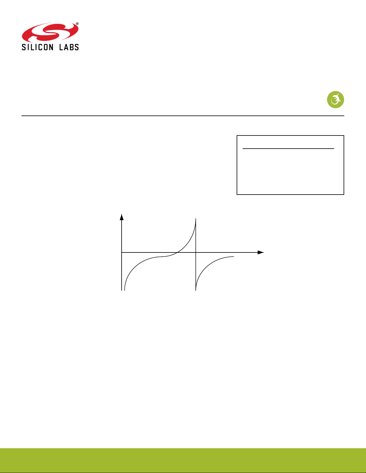
Reactance
KEY POINTS
• Learn which parameters are important
when selecting an oscillator.
• Learn how to properly configure a crystal
oscillator for use with MCU Series 1 or
Wireless SoC Series 1 devices.
f
S
f
A
Frequency
silabs.com | Building a more connected world. Rev. 1.34
Page 2

AN0016.1: Oscillator Design Considerations
1. Device Compatibility
This application note supports multiple device families, and some functionality is different depending on the device.
MCU Series 1 consists of:
• EFM32 Jade Gecko (EFM32JG1/EFM32JG12)
• EFM32 Pearl Gecko (EFM32PG1/EFM32PG12)
• EFM32 Giant Gecko (EFM32GG11)
Wireless SoC Series 1 consists of:
• EFR32 Blue Gecko (EFR32BG1/EFR32BG12/EFR32BG13/EFR32BG14)
• EFR32 Flex Gecko (EFR32FG1/EFR32FG12/EFR32FG13/EFR32FG14)
• EFR32 Mighty Gecko (EFR32MG1/EFR32MG12/EFR32MG13/EFR32MG14)
Z-Wave Modem SoC Series 1 consists of:
• EFR32 Zen Gecko (EFR32ZG13L/EFR32ZG13S/EFR32ZG14)
Device Compatibility
silabs.com | Building a more connected world. Rev. 1.34 | 2
Page 3

AN0016.1: Oscillator Design Considerations
Oscillator Theory
2. Oscillator Theory
2.1 What is an Oscillator?
An oscillator is an electronic circuit which generates a repetitive, or periodic, time-varying signal. In the context of MCU Series 1 or
Wireless SoC Series 1 devices, this oscillator signal is used to clock execution of instructions and peripherals in the device. For radio
communication the oscillator also provides an accurate and low noise frequency reference to the transciever. There are multiple ways
of generating such a signal, each with different properties that influence project cost, board size, and stability of the clock signal.
RC oscillators
RC oscillators are built from resistors, capacitors, and an inverting amplifier. They come at a low cost and have a shorter startup time
than the crystal oscillator, but are generally less accurate and produce more noise. The MCU Series 1 or Wireless SoC Series 1
devices provide multiple internal RC-oscillators including one high frequency RC oscillator (HFRCO) and one low frequency RC oscillator (LFRCO). While the internal RC-oscillators will ensure proper operation of the MCU Series 1 or Wireless SoC Series 1 device,
they are inadequate for applications such as radio communication.
Crystal oscillators
Crystal oscillators use the mechanical vibration of a crystal to generate the clock signal. Due to the molecular composition of the crystal matter and the angle of which the crystal is cut, this type of oscillator is very precise and stable over a wide temperature range. The
most commonly used crystal is the quartz crystal. Producing quartz crystals requires very stable temperature and pressure conditions
over a few weeks. This makes crystal oscillators more expensive than RC oscillators.
2.1.1 Piezoelectricity
Quartz crystals hold the direct piezoelectric property. This means an applied electric field will cause the crystal to deform. Conversely, a
deformation of the crystal will cause a voltage across the terminals. Once the oscillator has started, the changing voltage on the terminals of the vibrating crystal is used as the clock signal.
silabs.com | Building a more connected world. Rev. 1.34 | 3
Page 4
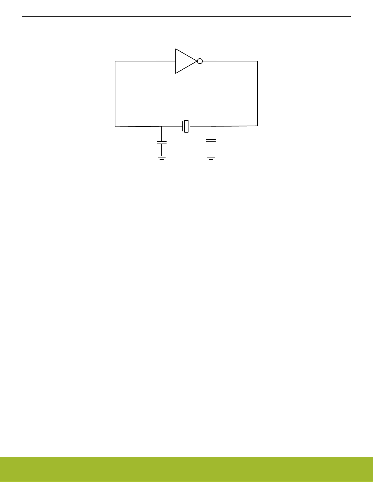
2.2 Basic Principle of Oscillators
AN0016.1: Oscillator Design Considerations
Oscillator Theory
Figure 2.1. Simplified Feedback Oscillator Loop
The principle behind the oscillator is a positive feedback loop satisfying the Barkhausen condition: If the closed-loop gain is larger than
unity and the total phase lag is 360°, the resulting closed-loop system is unstable and will self-reinforce. This is a necessary, but not
sufficient, condition for oscillations to be present. When the necessary conditions are met, any disturbance (noise) in the oscillator will
cause oscillations to start. The frequency that fulfills the Barkhausen condition is amplified the most, because it is in phase with the
original signal.
The initial oscillations are very weak and it takes time to amplify the signal to the desired magnitude. When oscillations are established,
only a small amount of energy is needed to compensate for losses in the circuit. Mathematically, a closed-loop gain of one is required to
maintain steady state oscillations. The MCU Series 1 or Wireless SoC Series 1 relies on an adjustable current source controlled by
automatic gain controller to achieve and maintain the desired amplitude.
Figure 2.1 Simplified Feedback Oscillator Loop on page 4 shows that the oscillator circuitry consists of two parts; an amplification stage
and a filter that decides which frequency experience a 360° phase lag. In the case of a crystal oscillator, the filter consists of the crystal
and external load capacitors.
2.2.1 Startup time
The magnitude of the closed-loop gain has great influence on the startup time. Low gain can cause excessively long startup time or
failure, and too high gain can startup to fail altogether. The ideal gain is dependent on the negative resistance of the oscillator circuit,
which is defined in Negative Resistance.
For the same reason, the oscillation frequency influences the startup time. A crystal in the kHz range would have a considerably longer
startup time than a crystal in the MHz range because the time it takes to circulate the loop is longer. Typical startup times for the MCU
Series 1 or Wireless SoC Series 1 are 200-400 ms for the low frequency oscillator and 200-400 µs for the high frequency oscillator.
silabs.com | Building a more connected world. Rev. 1.34 | 4
Page 5
AN0016.1: Oscillator Design Considerations
Oscillator Theory
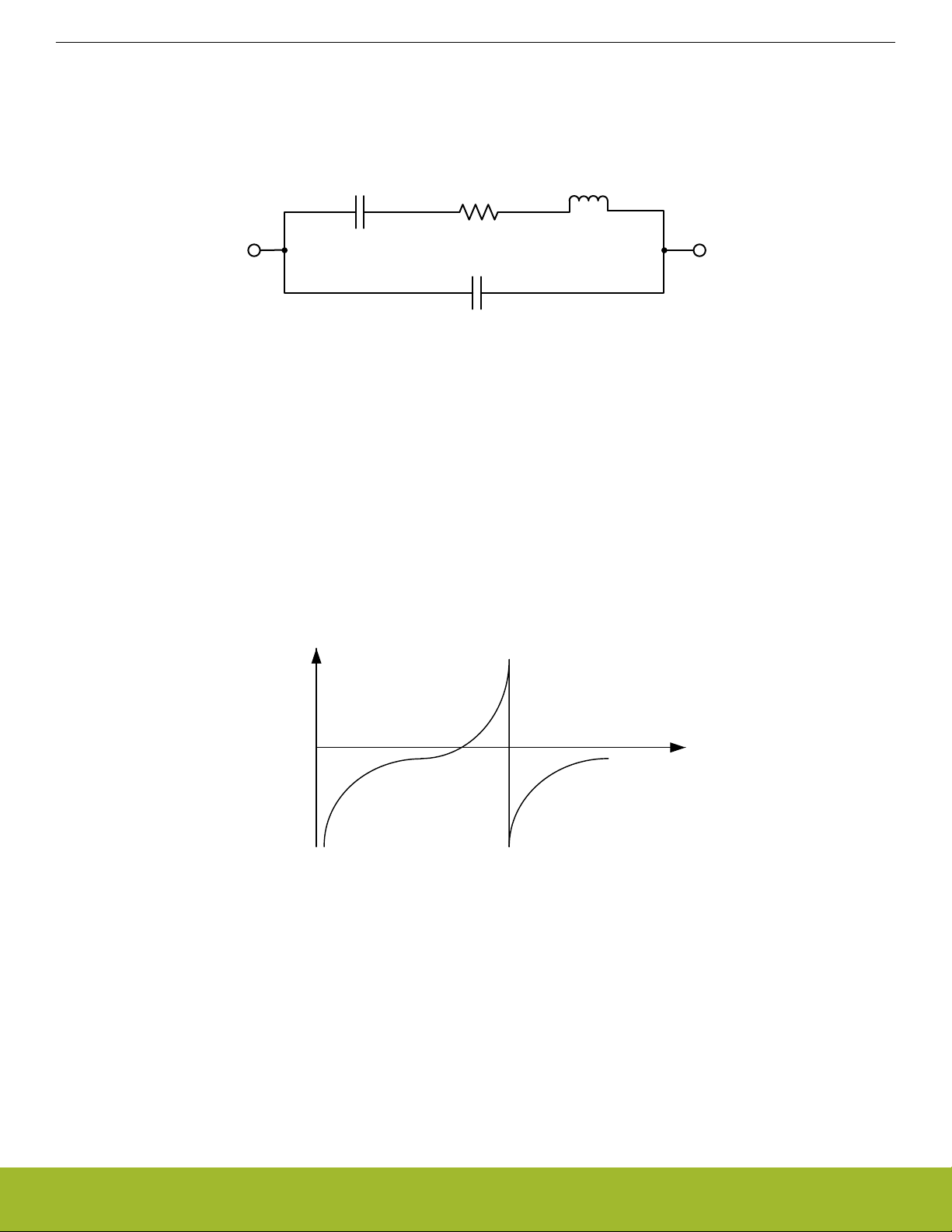
2.3 Modeling the Crystal
The crystal can be described by the electrical equivalent circuit in Figure 2.2 The Electrical Equivalent Circuit of a Crystal on page 5.
Cs
Rs
Ls
C0
Figure 2.2. The Electrical Equivalent Circuit of a Crystal
• CS is the motional capacitance. It represents the piezoelectric charge gained from a displacement in the crystal.
• RS is the motional resistance. It represents the mechanical losses in the crystal.
• LS is the motional inductance. It represents the moving mass in the crystal.
• C0 is the shunt capacitance between the electrodes and stray capacitance from the casing.
For low frequencies, the electrical equivalent circuit will exhibit capacitive behavior as depicted in Figure 2.3 Reactance vs. Frequency
on page 5. The presence of the inductor becomes more noticeable as the frequency, and thus the reactance, increases. Ignoring the
shunt capacitance C0, the series resonant frequency is defined where the reactance of the inductor and capacitor cancels. At this frequency the crystal appears only resistive with no shift in phase. The series resonance frequency, fS, therefore determines the relationship between CS and LS. This can be calculated with the equation below. The series resonance frequency is the natural resonance
frequency where the energy transformation between mechanical and electrical energy is most effective.
Reactance
f
S
Figure 2.3. Reactance vs. Frequency
f
A
Frequency
silabs.com | Building a more connected world. Rev. 1.34 | 5
Page 6

AN0016.1: Oscillator Design Considerations
Oscillator Theory
fS=
2 × π ×(LS× C
(
At higher frequencies, the equivalent circuit will appear inductive, which implies higher impedance. When the inductive reactance from
the crystal cancels the capacitive reactance from shunt capacitance C0, another resonance frequency with zero phase shift exists. This
frequency is called the anti-resonant frequency, fA. At this frequency, the impedance is 0.
fA=
2 × π ×(LS×
(
The range of frequencies between fS and fA is called the area of parallel resonance and is where the crystal will normally oscillate. At
the resonant frequency, the phase lag in the feedback loop is provided by an amplifier with 180° phase lag and two capacitors with a
combined 180° phase lag. In practice, the amplifier provides a little more than 180° phase shift, which means the crystal has to appear
slightly inductive to fulfill the Barkhausen criterion.
2.3.1 Series and Parallel Resonant Crystals
Physically there is no difference between series and parallel resonant crystals. Series resonant crystals are specified to oscillate at the
series resonant frequency where the crystal appears with no reactance. Because of this, no external capacitance should be present as
this would lower the oscillating frequency to below the natural resonance frequency. These crystals are intended for use in circuits with
no external capacitors where the oscillator circuit provides 360° phase shift.
Parallel resonant crystals require a capacitive load to oscillate at the specified frequency and this is the resonance mode required for
MCU Series 1 or Wireless SoC Series 1 devices. On MCU Series 1 or Wireless SoC Series 1 devices, the load capacitors are located
on-chip, and their values can be controlled by firmware. Thus, MCU Series 1 or Wireless SoC Series 1 devices do not require external
load capacitors, reducing BOM cost and saving PCB space. The exact oscillation frequency for a parallel resonant crystal can be calculated with the equation below, where CL is the load capacitance seen by the crystal. CL is therefore an important design parameter and
is given in the datasheet for parallel resonant crystals.
1
1
CS× C
CS+ C
1
2
)
)
S
1
0
2
)
)
0
fP= f
C
2 × C
S
)
L
1 +
S
(
silabs.com | Building a more connected world. Rev. 1.34 | 6
Page 7

AN0016.1: Oscillator Design Considerations
MCU Series 1 or Wireless SoC Series 1 Crystal Oscillators
3. MCU Series 1 or Wireless SoC Series 1 Crystal Oscillators
The MCU Series 1 or Wireless SoC Series 1 devices include two crystal oscillators, the Low Frequency Crystal Oscillator (LFXO) and
the High Frequency Crystal Oscillator (HFXO). These oscillators require an external clock or crystal connected to the crystal oscillator
pins of the device, however, no external crystal load capacitors are required as they contain on-chip tunable load capacitors. The LFXO
supports crystals with a nominal frequency of 32.768 kHz, while the HFXO supports 4-50 MHz depending on the device, see datasheet
for more information. External oscillators which provide sine waves are also supported. Both the high and low frequency clock sources
can be used simultaneously.
In the MCU Series 1 or Wireless SoC Series 1 oscillator circuits are designed as a Pierce oscillator as shown in Figure 3.1 The Pierce
Oscillator in the MCU Series 1 or Wireless SoC Series 1 on page 7.
EFx32
XTAL
P
R
0
R
XTAL
N
C
L1
C
L2
out
g
m
Figure 3.1. The Pierce Oscillator in the MCU Series 1 or Wireless SoC Series 1
The Pierce oscillator is known to be stable for a wide range of frequencies and for its low power consumption.
The MCU Series 1 or Wireless SoC Series 1 crystal oscillators use a relatively low oscillation amplitude, which can lead to a lower
oscillation frequency than stated as the nominal value in the crystal's datasheet. More information on this effect is given in 5.4 Frequen-
cy Pulling.
3.1 Timeout
To ensure that the XO clock signals are not used internally in the MCU Series 1 or Wireless SoC Series 1 before they are stable, both
the HFXO and the LFXO include a configurable timeout. When the XO starts up, the timeout counter will count to the configured number of cycles before the clock signal propagates to the internal clock trees and the digital logic.
silabs.com | Building a more connected world. Rev. 1.34 | 7
Page 8

AN0016.1: Oscillator Design Considerations
MCU Series 1 or Wireless SoC Series 1 Crystal Oscillators
3.2 Oscillator Configuration
The LFXO/HFXO can be easily configured by leveraging the emlib library. The library contains oscillator initialization structures and
functions which abstract the software options available for each oscillator.
At the register level, the HFXO and LFXO oscillation start-up on MCU Series 1 or Wireless SoC Series 1 devices are controlled by the
CMU_HFXOCTRL, CMU_HFXOxxxCTRL, and CMU_LFXOCTRL registers. See the specific product reference manual for detailed register level desriptions of the configuration options available for the external oscillators.
For MCU Series 1 devices, there is an HFXO configuration spreadsheet available for download from https://www.silabs.com/communi-
ty/mcu/32-bit/knowledge-base.entry.html/2018/09/20/hfxo_selection_andc-yqMU. The Knowledge Base article was written for
EFM32GG11, but with the exception of the maximum frequency range, is relevant for the compatible MCU Series 1 devices mentioned
in this Application Note. The article and spreadsheet highlight the required parameters needed from a potential crystal oscillator candidate, and provide optimal HFXO register settings to properly tune, optimize power consumption, and ensure reliable operation based on
the oscillator manufacturer's specifications. The functions within emlib library assist in proper setup of these registers.
Wireless SoC Series 1 devices support a narrower range of HFXO frequencies, with 38.4 MHz recommended for most wireless applications to meet transceiver electrical specifications, and 39 MHz recommended for implementing Z-Wave devices. The default settings in
the emlib library and Silicon Labs protocol stacks are recommended. [Application Builder] is a wireless project development tool in
Simplicity Studio that will automatically configure the clock settings with the proper default values based on the selected wireless protocol.
Simplicity Studio also contains a tool, [Hardware Configurator], to assist users when configuring both load capacitance and software
settings for using the LFXO and the HFXO. Once the correct hardware configuration has been found [Hardware Configurator] generates C-code which can be used within an application to implement variances from default configurations.
3.2.1 LFXO Gain Setting Recommendations
When setting the GAIN value in the CMU_LFXOCTRL register, the following guidelines should be observed:
• C0 must be ≤ 2pF
• For 12.5 pF ≤ CL ≤ 18 pF, set GAIN = 3
• For 8 pF ≤ CL ≤ 12.5 pF, set GAIN = 2
• For 6 pF ≤ CL ≤ 8 pF, set GAIN = 1
• For CL ≤ 6 pF, set GAIN = 0
The GAIN setting affects oscillator bias current during the startup phase only. Following these guidelines will allow for maximum transconductance gain (gm) during the LFXO startup phase, ensuring a fast and robust startup.
3.3 External Clock and Buffered Sine Input
The HFXO and LFXO oscillators can be used as inputs for an externally generated digital clock signal. When using the oscillators in this
way, connect the clock input to HFXTAL_N or LFXTAL_N. The max frequency of these inputs are limited by the max clock frequency of
the device (see the device data sheet for more information). An externally buffered sine signal can also be applied to the HFXTAL_N or
LFXTAL_N pin. The recommended amplitude of this signal is between 0.8 and 1.2 V
, and the frequency must be the same as re-
pk-pk
quired when using crystals with the HFXO and LFXO.
silabs.com | Building a more connected world. Rev. 1.34 | 8
Page 9

AN0016.1: Oscillator Design Considerations
Z-Wave Modem SoC Series 1 Crystal Oscillators
4. Z-Wave Modem SoC Series 1 Crystal Oscillators
The Z-Wave Modem SoC Series 1 devices include a High Frequency Crystal Oscillator (HFXO). The oscillator requires an external
clock or crystal connected to the crystal oscillator pins of the device, however, no external crystal load capacitors are required as tunable load capacitors are contained on-chip.
The Z-Wave Modem SoC Series 1 devices share common oscillator design and theory with MCU Series 1 or Wireless SoC Series 1.
However, due to the strict frequency requirements for Z-Wave, the supported HFXO frequency is limited to 39.0 MHz and the crystal
specifications are more stringent. The oscillator settings for the devices are preconfigured for this frequency, with a limited subset of
configurable options. The most pertinent portion of this document for designs with Z-Wave Modem SoC Series 1 is the recommended
crystal section Table 8.4 39 MHz Crystals on page 17.
For more information regarding crystal specifications and configuration and calibration of the crystal oscillator for Z-Wave Modem SoC
Series 1 devices please refer to the product datasheet, along with INS14487: Z-Wave Integration Guide, INS14498: Mandatory Crystal
Adjustment for EFR32ZG14 Based Products, and INS14283: Instruction for Bring-up/Test HW Development.
silabs.com | Building a more connected world. Rev. 1.34 | 9
Page 10

AN0016.1: Oscillator Design Considerations
Crystal Parameters
5. Crystal Parameters
5.1 Quality Factor
The quality factor Q is a measure of the efficiency or the relative storage of energy to dissipation of energy in the crystal. For the electrical-equivalent circuit, the equation below states the relation between R, C and Q. In practice, crystals with higher Q-values are more
accurate, but have a smaller bandwidth for which they oscillate. Therefore, high Q-factor crystals will start slower than crystals with
higher frequency tolerance.
X
LS
Q =
X
L
S
5.2 Load Capacitance
As seen in the equation below, the two capacitors CL1 and CL2 provide capacitive load for the crystal. The effective load capacitance,
CL, as seen from the HFXTAL_N and HFXTAL_P pins on the MCU Series 1 or Wireless SoC Series 1 is the series combination of C
and CL2 through ground.
CL=
Where C
Right choice of CL is important for proper operating frequency. Crystals with small load capacitance would typically start faster than
crystals requiring a large CL. Large load capacitors also increase power consumption. It is recommended to use a crystal with CL as
specified in 8. Recommended Crystals. The MCU Series 1 or Wireless SoC Series 1 device datasheets also contain more information
on the allowed load capacitance range.
Note: The MCU Series 1 or Wireless SoC Series 1 devices have internal loading capacitors and do not need external capacitors connected to the crystal. See the device data sheet or reference manual for more information.
5.3 Equivalent Series Resistance
R
S
and X
CL1× C
(
CL1+ C
(
=
C
stray
1
XCS× R
(
are the reactance of LS and CS, respectively, at the operating frequency of the crystal.
S
)
L2
)
L2
is the pin capacitance of the microcontroller and any parasitic capacitance, and can often be assumed in the range 2-5 pF.
+ C
=
2 × π × f × CS× R
)
(
S
stray
1
=
)
S
2 × π × f × L
R
S
S
L1
The Equivalent Series Resistance is the resistance in the crystal during oscillation and varies with the resonance frequency. ESR, given
by the equation below, will typically decrease with increasing oscillation frequency.
2
C
ESR = R
The HFXO/LFXO circuits of the MCU Series 1 or Wireless SoC Series 1 cannot guarantee startup of crystals with ESR larger than a
certain limit. Please refer to the device datasheet for further details. The smaller the ESR, compared to this maximum value, the better
gain margin for startup of the crystal which in turn reduces the startup time. Additionally, a small ESR value gives lower power consumption during oscillation.
Note that HF crystals have ESR of a few tens of Ohms as compared to the LF crystals which have ESR values normally measured in
kOhm. Therefore a few Ohm of series resistance has more influence on the startup margin in the MHz range as compared to the kHz
range.
S
(
1 +
0
)
C
L
silabs.com | Building a more connected world. Rev. 1.34 | 10
Page 11

AN0016.1: Oscillator Design Considerations
Crystal Parameters
5.4 Frequency Pulling
As the crystal oscillators in the MCU Series 1 or Wireless SoC Series 1 use a relatively low oscillation amplitude, the oscillation frequency can be lower than stated in the datasheet when using the suggested load capacitance. This offset is best found by measuring
the resulting frequency when using the suggested load capacitance. The offset will be stable and not affected by temperature, voltage
or aging. If it is desirable to achieve the nominal frequency given for the crystal, there are two options:
• Option A — Order a crystal from the crystal vendor that has a nominal frequency equal to the frequency you want to achieve plus
the measured offset frequency.
• Option B — It is possible to slightly alter the oscillation frequency of a crystal by adjusting the load capacitance (CL1 and CL2). The
pullability of the oscillation system refers to which extent it is possible to tune the resonance frequency of the crystal by changing
these values. The crystal sees these capacitors in series through ground, parallel to the closed loop. They will therefore slightly alter
the anti-resonance frequency of the crystal. The equation below shows the pullability in terms of frequency change in ppm per
change in combined load capacitance in pF.
Average pullability (ppm/pF) =
5.5 Drive Level
Drive level is a measure of the power dissipated in the crystal. The crystal manufacturer should specify the maximum power dissipation
value tolerated by the crystal in the crystal datasheet. Exceeding this value can damage the crystal.
DL = ESR × I
Here, I is the RMS current flowing through the crystal.
5.6 Minimum Negative Resistance
A critical condition for oscillations to build up requires the energy supplied to exceed the energy dissipated in the circuit. In other words,
the negative resistance of the amplifier has to exceed the equivalent series resistance in the crystal. An approximate formula for negative resistance is given in the equation below.
R
=
neg
Where gm is the transconductance of the oscillator circuitry. To ensure safe operation over all voltage and temperature variations, ensure that the ESR does not exceed the device datasheet maximum. This maximum value corresponds to the oscillator circuit's realiza-
ble negative resistance.
2
-g
m
(2 × π × f )2× CL1× C
(
CS× 10
2 ×(C0+ C
)
L2
6
2
)
L
If the crystal ESR does not satisfy this criterion, another crystal with lower ESR should be chosen. The equation above shows an approximate formula for this calculation which excludes shunt capacitance and internal loss.
5.7 Frequency Stability
Frequency stability is the maximum frequency deviation from the specified oscillating frequency over the given operating temperature
range.
5.8 Frequency Tolerance
Frequency tolerance is the maximum frequency deviation from the specified oscillating frequency at 25 °C. This parameter gives an
indication of variations between individual crystals.
5.9 PCB Layout
To minimize noise sensitivity caused by parasitic antenna and spurious coupling phenomena, the distance between the crystal, and the
MCU Series 1 or Wireless SoC Series 1 oscillator pins should be as short as possible. If it is not possible to place the external oscillator
components close to the oscillator pins, care should be taken when routing these signals. Avoid long traces underneath the MCU Series 1 or Wireless SoC Series 1 package and other circuitry that could create spurious coupling with logic activity. Also avoid routing any
other signals through the crystal area.
Ensure that the ground plane underneath the oscillator is of good quality. Do not use a separate ground plane under the oscillator with
a narrow connection to the reference ground as this can act as an antenna. To avoid coupling from surrounding signal traces, it is a
good practice to place a grounded guard ring around the oscillator and its components.
silabs.com | Building a more connected world. Rev. 1.34 | 11
Page 12

AN0016.1: Oscillator Design Considerations
Reducing Power Consumption
6. Reducing Power Consumption
The power consumption of the crystal oscillator is mostly determined by the drive level of the oscillator. This equals the power dissipated in the crystal as given in the equation below.
1
DL =
Vpp is the peak to peak voltage across the crystal at the resonance frequency.
Because the internal buffer draws some current regardless of clock frequency, the average power consumption per MHz is usually lower for high clock frequencies. In the energy conscious sense it is therefore favorable to alternate between short periods in run mode
with HFXO enabled and lower energy modes where HFXO is not running.
During startup the current consumption is higher than after oscillations have stabilized. A short startup time reduces the period in which
the current consumption of the oscillator is high and is therefore essential if the oscillator is frequently switched on and off. In general
one would like the circuit to be operational as fast as possible and a fast startup time is therefore favorable. Crystals with low ESR and
load capacitance typically have the shortest startup time and consume the least amount of power.
× ESR ×(2 × π × f × Vpp×(C0+ C
2
2
))
L
silabs.com | Building a more connected world. Rev. 1.34 | 12
Page 13

AN0016.1: Oscillator Design Considerations
Considerations for Radio Applications with the MCU Series 1 or Wireless SoC Series 1 Portfolio
7. Considerations for Radio Applications with the MCU Series 1 or Wireless SoC Series 1 Portfolio
7.1 General Notes
This section adds a few details about specific requirements related to wireless applications.
While MCU Series 1 or Wireless SoC Series 1 devices support a range of 38 to 40 MHz for the HFXO, the recommended value is 38.4
MHz. For our Z-Wave products, the recommended value is 39.0 MHz. Transceiver electrical specifications are based on these frequencies, and Silicon Labs protocol stacks use these as the default.
The crystal frequency tolerance is determined by various aspects of the design:
Required frequency tolerance of the protocol
For example 802.15.4 applications require ±40 ppm accuracy under all conditions.
Temperature range
The S-shaped temperature characteristic of AT-cut crystals becomes steeply negative at low temperatures, steeply positive at high
temperatures. A larger temperature range requires a specific cut angle of the crystal to bound the absolute accuracy. Most crystals are
specified from -40 °C to +85 °C, but some applications may require operation up to 105 °C or 125 °C ambient temperature.
Manufacturing accuracy
Individual crystals have a frequency error at 25 °C. This is typically specified as ±10 ppm "manufacturing tolerance" or "make tolerance". This error adds to the temperature error.
Aging tolerance
Crystals drift over time, typically 1-2 ppm per year. Excessive heat during assembly or from hand soldering may also prematurely age
a crystal.
The allowable frequency error of the crystal is the sum of temperature, board-to-board, and crystal-to-crystal variations.
7.2 Crystal Loading and Production Tuning
The load capacitance, CL, is implemented on-chip by two tunable capacitors. External capacitors are neither required nor recommended.
The load capacitor tuning range in pF is given in the datasheet by C
with a resolution of SS
HFXO_T
per step. The resulting frequen-
HFXO
cy per step depends on the crystal's pulling sensitivity and the shunt capacitance of the oscillator circuit.
7.2.1 Tuning Strategies
The on-chip variable load capacitor may be used in one of two ways.
• A fixed value may be used for all units. During design a number of units should be characterized and an average center CTUNE
value determined. Some crystal vendors may provide characterized samples to help tune to the center of the crystal distribution. In
corner cases the remaining error should be in the order of a few ppm only, depending on manufacturing spread (PCB parasitics,
component variation, etc.).
• Each unit may also be calibrated in production. A unique value of CTUNE is determined per unit and stored in flash memory. This
calibrates out the manufacturing error of the crystal, leaving only the temperature error and aging components. This may allow the
system to operate across a broader temperature range or with a less accurate crystal at the expense of production calibration time.
The variable on-chip loading capacitor can theoretically be used to offset temperature-induced errors as well. While simple in concept
this is difficult in practice primarily due to temperature characteristic differences from crystal to crystal.
Crystal ppm error can be measured by outputing a clock signal to a GPIO pin. This process, along with example code demonstrating
oscillator calibration, is described in AN0004.2: EFR32 Series 2 Wireless MCU Clock Management Unit (CMU)
7.3 PCB Layout
The crystal section PCB layout should be kept compact and close to the IC. Longer traces increase possibility of spurious transmission
and increase the fixed parasitic loading capacitance. The crystal's case ground pins should be grounded. Please refer to AN928:
"EFR32 Layout Design Guide" for further notes on this subject. Application notes can be found on the Silicon Labs website (www.si-
labs.com) or in Simplicity Studio.
7.4 External Tuning Capacitance
All required crystal loading capacitance is on-chip, therefore, external loading capacitors are not recommended.
silabs.com | Building a more connected world. Rev. 1.34 | 13
Page 14

AN0016.1: Oscillator Design Considerations
Considerations for Radio Applications with the MCU Series 1 or Wireless SoC Series 1 Portfolio
7.5 External Oscillator Operation
For narrowband applications the system reference frequency may be provided by an external oscillator such as a Temperature Compensated Crystal Oscillator (TCXO). The TCXO output is connected to the HFXTAL_N pin and the mode field is set to
cmuHfxoOscMode_ExternalSine in the em_lib HFXO initialization struct.
7.5.1 TCXO Phase Noise Recommendations
When using a 38.4 MHz TCXO in a radio application, designers must ensure that phase noise in the system meets or exceeds the
performance measurements below (i.e. is less than these figures) in order to avoid phase noise related performance degradation.
Table 7.1. TCXO Phase Noise Referenced to 38.4 MHz Fundamental Frequency
Offset From 38.4 MHz Carrier Phase Noise (dBc/Hz)
1 kHz Offset -123
3 kHz Offset -132
10 kHz Offset -134
30 kHz Offset -136
100 kHz Offset -145
1 MHz Offset -148
10 MHz Offset -140
silabs.com | Building a more connected world. Rev. 1.34 | 14
Page 15

AN0016.1: Oscillator Design Considerations
Recommended Crystals
8. Recommended Crystals
8.1 General Notes for Crystal Selection
When deciding upon which crystal to employ, the following considerations could be helpful to ensure a proper functioning oscillator.
Operating environment
Temperature, humidity, and mechanical vibration affect the stability properties. For crystals, define what crystal cut is most appropriate
for the application. For most applications, AT cut is an excellent choice due to good temperature stability over a wide temperature
range. SC cut has good stability when exposed to mechanical vibrations, but suffers from humidity and temperature changes. Many
more cuts with different properties exists.
Package
Surface mount or through-hole. If size is critical, define maximum package dimensions.
Find load capacitors
Ensure that CL is within range specified by the MCU Series 1 or Wireless SoC Series 1 datasheet.
Calculate negative resistance
If the magnitude of the negative resistance is less than 2xESR
The recommended crystals are chosen from a selection of popular crystals with different ESR, cost, frequency stability, and tolerance.
By examining the list of considerations above, one should be able to find a suitable crystal.
All the recommended crystals are fundamental mode, as is recommended for MCU Series 1 or Wireless SoC Series 1.
, then find another crystal or adjust the load capacitance.
max
silabs.com | Building a more connected world. Rev. 1.34 | 15
Page 16

AN0016.1: Oscillator Design Considerations
Recommended Crystals
8.2 Crystal Specifications for MCU Series 1 or Wireless SoC Series 1
The following crystals may be considered for use with MCU Series 1 or Wireless SoC Series 1. Suitability for a particular application
should be verified. Different frequency tolerance / temperature ranges may be available. Contact the crystal vendor for details.
Table 8.1. 38.4 MHz Crystals
Mfg Part ESR (Ω) C0 (max)
Temp (°C) Temp
(pF)
KDS DSX211SH
50 2 -40 to +85 ± 20 ± 10 10 1.6 x 2.0
1ZZHAE38400AB0A
KDS DSX211SH
1ZZHAE38400AB0B
50 2 -40 to
+105
Kyocera CX2016DB38400F0FSRC1 40 1 -40 to
+125
Kyocera CX2520DB38400F0FSRC2 50 1.2 -40 to
+125
Kyocera CX2520DB38400F0FSRC3 40 1.2 -40 to
+125
NDK EXS00A-CS08361 40 1.26 -40 to
+125
NDK NX2016SA-38.4MHz-
60 0.61 -30 to +85 ± 12 +-10 10 1.6 x 2.0
EXS00A-CS08973
TaiSaw TZ0909E 50 3 -40 to
+125
TaiSaw TZ2205E 40 3 -40 to
+125
Tolerance
(ppm)
Mfg
Tolerance
(ppm)
CL (pF) Footprint
± 20 ± 10 10 1.6 x 2.0
± 40 ± 10 10 1.6 x 2.0
± 40 ± 10 10 2.0 x 2.5
± 40 ± 10 10 2.0 x 2.5
± 32 ± 10 10 2.0 x 2.5
± 30 ± 10 10 2.0 x 2.5
± 30 ± 10 10 1.6 x 2.0
(mm)
Table 8.2. 38.4 MHz TCXOs
Mfg Part Supply
Voltage (V)
NDK NT2016SA-38.4MHz-
1.8 to 3.6 0.8 -40 to
END5109A
Output
Voltage
(V
pk-pk
Temp (°C) Current
Consumption
)
+105
Frequency
Footprint
Tolerance
(mA)
(ppm)
1.7 ± 2 1.6 x 2.0
Table 8.3. 32768 Hz Crystals
Mfg Part ESR (kΩ) C0 (typ)
Temp (°C) Tolerance (ppm) CL (pF) Footprint
(pF)
Abracon
ABS07-32.768KHZ-7 70 1.2 -40 to +85 ± 20 7 3.2 x 1.5
Corporation
Epson FC-135 65 1.0 -40 to +85 ± 20 9 3.2 x 1.5
KDS DST210AC 70 1.3 -40 to +85 ± 20 7.0 2.0 x 1.2
KDS DST310S 70 1.3 -40 to +85 ± 20 12.5 3.2 x 1.5
Micro Crys-
CM8V-T1A 55 1.1 -40 to +85 ± 20 13 2.0 x 1.2
tal
(mm)
(mm)
silabs.com | Building a more connected world. Rev. 1.34 | 16
Page 17

AN0016.1: Oscillator Design Considerations
Recommended Crystals
8.3 Crystal Specifications for Z-Wave Modem SoC Series 1
The following crystals may be considered for use with Z-Wave Modem SoC Series 1. Suitability for a particular application should be
verified. Different frequency tolerance / temperature ranges may be available. Contact the crystal vendor for details.
Table 8.4. 39 MHz Crystals
Mfg Part ESR (Ω) C0 (max)
(pF)
Temp (°C) Temp
Tolerance
(ppm)
Mfg
Tolerance
(ppm)
CL (pF) Footprint
(mm)
Siward XTL501140-S315-020 50 3 -40 to +90 ± 14 ± 8 10 1.6 x 2.0
TXC 8Y39072002 35 1.0 -40 to +95 ± 13 ± 8 10 1.6 x 2.0
Note: The crystal is a critical component of Z-Wave devices and calibration is mandatory for gateway designs. Please refer to
INS14498: Mandatory Crystal Adjustment for EFR32ZG14 Based Products for additional information.
Table 8.5. 39 MHz TCXOs
Mfg Part Supply
Voltage
(V)
Kyocera KT2016K39000ZAZ18TAVG41.8 ± 5% Clipped
Output
Type
Sine
Output
Voltage
(V
)
pk-pk
0.8 -40 to
Temp
(°C)
+115
Current
Consumption
(mA)
Frequency
Tolerance
(ppm)
± 27 2 1.6 x 2.0
Footprint
(mm)
Wave
Siward TXO973270-STO-4932 1.68 to
3.63
HCMOS
Square
Wave
— -40 to
+115
-40 to
± 20 5.5 1.6 x 2.0
± 27
+125
silabs.com | Building a more connected world. Rev. 1.34 | 17
Page 18

AN0016.1: Oscillator Design Considerations
Revision History
9. Revision History
Revision 1.34
June, 2020
• Added DST210AC to Table 8.3 32768 Hz Crystals on page 16
• Fixed minor typos throughout the document
Revision 1.33
June, 2020
• Added EFR32ZG13L and EFR32ZG13S to 1. Device Compatibility.
• Updated Table 8.4 39 MHz Crystals on page 17 for Z-Wave devices (AN0016.1).
• Added Table 8.5 39 MHz TCXOs on page 17 with recommendations for Z-Wave devices (AN0016.1).
Revision 1.32
October, 2019
• Updated Table 8.3 32768 Hz Crystals on page 16. Removed crystals that exceeded Series 1 device max ESR specifications.
Revision 1.31
February, 2019
• Updated recommended crystals to include Table 8.4 39 MHz Crystals on page 17 for Z-Wave devices (AN0016.1).
• Added reference in Oscillator Configuration to a Knowledge Base article and spreadsheet which help configure HFXO register settings (AN0016.1).
• Removed redundant text.
• Updated 9. Revision History to adhere to new schema.
Revision 1.30
December, 2017
• Split application note into AN0016.0 and AN0016.1 for MCU Series 0 or Wireless MCU Series 0 and MCU Series 1 or Wireless SoC
Series 1 device families, respectively.
• Updated recommended crystals for MCU Series 1 or Wireless SoC Series 1 (AN0016.1).
• Improved graphics.
• Added MCU Series 1 or Wireless SoC Series 1 LFXO GAIN recommendations.
• Updated/added TCXO information, including recommended input voltage and phase noise measurements (AN0016.1).
Revision 1.29
June, 2017
• Moved the device compatibility information from the front page to 1. Device Compatibility.
• Updated the references to the various device families.
Revision 1.28
February, 2017
• Updated content for new naming convention.
• Updated Table 8.1 38.4 MHz Crystals on page 16 to add a new crystal option and a C0 column.
Revision 1.27
May, 2016
• Updated the Kyocera crystal ESR value in Table 8.1 38.4 MHz Crystals on page 16.
silabs.com | Building a more connected world. Rev. 1.34 | 18
Page 19

AN0016.1: Oscillator Design Considerations
Revision History
Revision 1.26
May, 2016
• Updated the Kyocera crystal information in and added a new TaiSaw crystal to Table 8.1 38.4 MHz Crystals on page 16.
• Changed fa to fA in Figure 2.3 Reactance vs. Frequency on page 5.
Revision 1.25
November, 2015
• Added support for the Wireless SoC Series 1
Revision 1.24
October, 2015
• Formatting update
• Added support for MCU Series 1
Revision 1.23
October, 2013
• New cover layout
Revision 1.22
May, 2013
• Added crystals from River Eletec Corporation.
• Removed DL numbers for recommended crystals as they were misleading.
Revision 1.21
April, 2012
• Corrected typos in XO Configurator description.
Revision 1.20
April, 2012
• Updated recommendations on minimum negative resistance and removed recommendations on gain margin.
• Added information on timeout counter and glitch detection.
• Added PCB layout recommendations.
• Added information on external clock and buffered sine input.
• Added information on XO Configuration in energyAware Designer. Removed recommendations on how to use LFXOBOOST in
CMU_CTRL as this is now covered by the eA Designer.
• Removed crystal selection spreadsheet.
• Added recommended 48 MHz crystals.
Revision 1.10
August, 2011
• Updated recommendations on use of LFXOBOOST.
• Updated recommended crystals in document and spreadsheet for LFXO.
Revision 1.00
July, 2010
• Initial revision.
silabs.com | Building a more connected world. Rev. 1.34 | 19
Page 20

Simplicity Studio
One-click access to MCU and
wireless tools, documentation,
software, source code libraries &
more. Available for Windows,
Mac and Linux!
IoT Portfolio
www.silabs.com/IoT
Disclaimer
Silicon Labs intends to provide customers with the latest, accurate, and in-depth documentation of all peripherals and modules available for system and software implementers using or
intending to use the Silicon Labs products. Characterization data, available modules and peripherals, memory sizes and memory addresses refer to each specific device, and "Typical"
parameters provided can and do vary in different applications. Application examples described herein are for illustrative purposes only . Silicon Labs reserves the right to make changes without
further notice to the product information, specifications, and descriptions herein, and does not give warranties as to the accuracy or completeness of the included information. Without prior
notification, Silicon Labs may update product firmware during the manufacturing process for security or reliability reasons. Such changes will not alter the specifications or the performance
of the product. Silicon Labs shall have no liability for the consequences of use of the information supplied in this document. This document does not imply or expressly grant any license
to design or fabricate any integrated circuits. The products are not designed or authorized to be used within any FDA Class III devices, applications for which FDA premarket approval is
required, or Life Support Systems without the specific written consent of Silicon Labs. A "Life Support System" is any product or system intended to support or sustain life and/or health,
which, if it fails, can be reasonably expected to result in significant personal injury or death. Silicon Labs products are not designed or authorized for military applications. Silicon Labs
products shall under no circumstances be used in weapons of mass destruction including (but not limited to) nuclear, biological or chemical weapons, or missiles capable of delivering
such weapons. Silicon Labs disclaims all express and implied warranties and shall not be responsible or liable for any injuries or damages related to use of a Silicon Labs product in such
unauthorized applications.
Trademark Information
Silicon Laboratories Inc.®, Silicon Laboratories®, Silicon Labs®, SiLabs® and the Silicon Labs logo®, Bluegiga®, Bluegiga Logo®, ClockBuilder®, CMEMS®, DSPLL®, EFM®, EFM32®,
EFR, Ember®, Energy Micro, Energy Micro logo and combinations thereof, "the world’s most energy friendly microcontrollers", Ember®, EZLink®, EZRadio®, EZRadioPRO®, Gecko®,
Gecko OS, Gecko OS Studio, ISOmodem®, Precision32®, ProSLIC®, Simplicity Studio®, SiPHY®, Telegesis, the Telegesis Logo®, USBXpress® , Zentri, the Zentri logo and Zentri DMS, ZWave®, and others are trademarks or registered trademarks of Silicon Labs. ARM, CORTEX, Cortex-M3 and THUMB are trademarks or registered trademarks of ARM Holdings. Keil is a
registered trademark of ARM Limited. Wi-Fi is a registered trademark of the Wi-Fi Alliance. All other products or brand names mentioned herein are trademarks of their respective holders.
Silicon Laboratories Inc.
400 West Cesar Chavez
Austin, TX 78701
USA
SW/HW
www.silabs.com/simplicity
Quality
www.silabs.com/quality
Support and Community
community.silabs.com
http://www.silabs.com
 Loading...