

SILAN SC9318FA, SC9318FB Datasheet
Silan
Semiconductors
DIGITAL TUNING SYSTEM
DESCRIPTION
The SC9318-033 is a single-chip digital tuning system optimum
for portable sets such as headphone radio, etc… 5-band of
FM/MW/LW/TV/SW are provided compatibly with worldwide
destinations.
FEATURE
Tuning function:
• Manual tuning (up/down)
• Direct tuning
• Seek tuning
Memory function:
• FM/MW/LW or TV/SW/WB each band 10 stations
Clock function:
• Dual clock function
• 12/24H clock
• Sleep timer function
• Alarm timer function
Other function:
Battery check input
HANGZHOU SILAN MICROELECTRONICS JOINT-STOCK CO.,LTD
1
SC9318-033
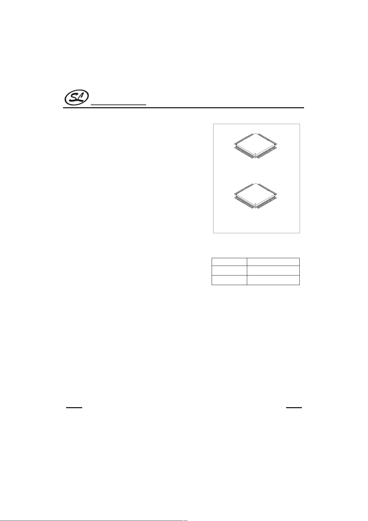
ORDERING INFORMATION
Device Package
SC9318FA LQFP-64-10x10–0.5
SC9318FB LQFP-64-12x12–0.65
LQFP-64-10x10-0.5
LQFP-64-12 x12-0.65
Rev: 1.0 2002-01-16
Silan
Semiconductors
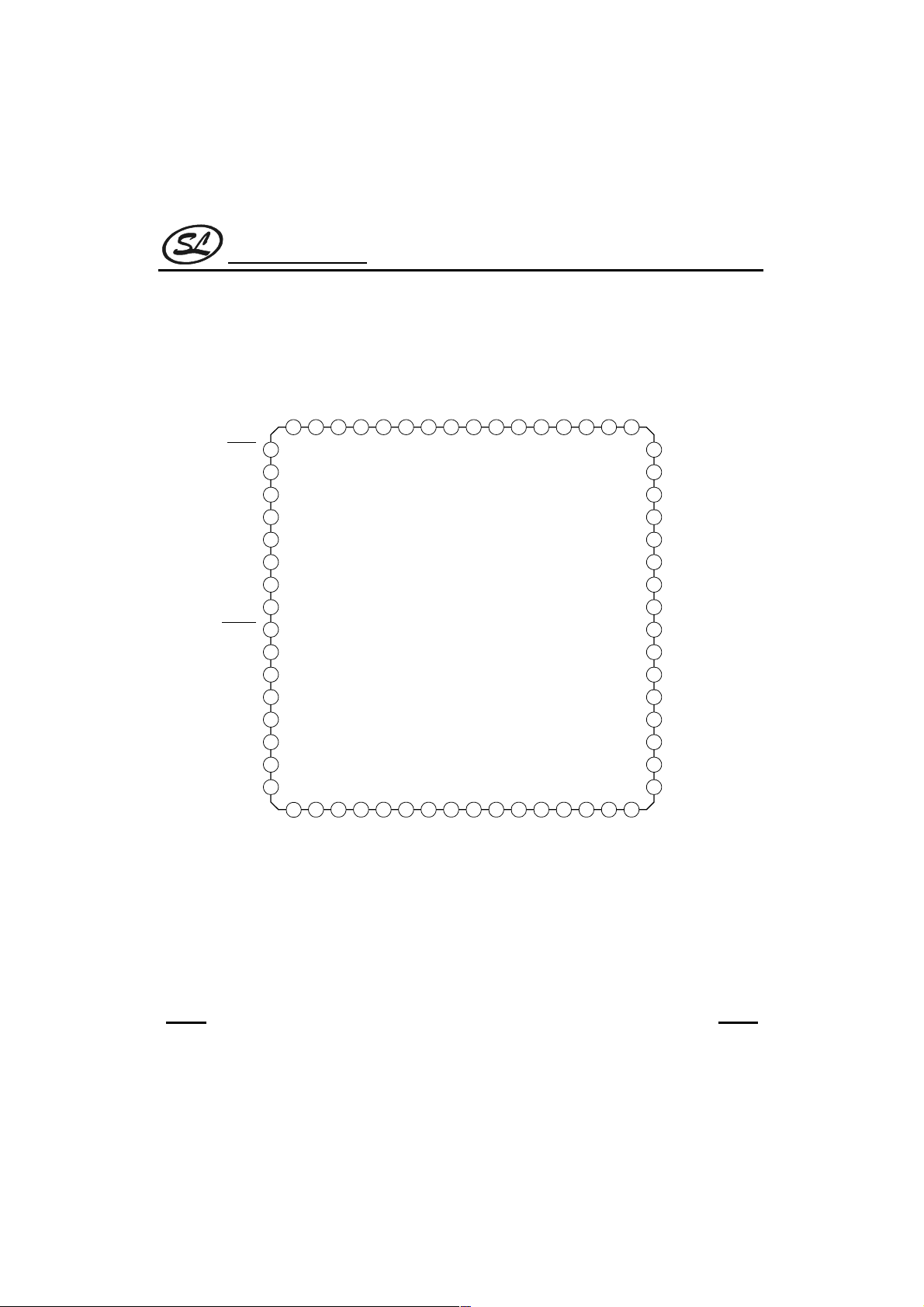
PIN CONFIGURATION
TEST
48 47 46 45 44 43 42 41 40 39 38 37
49
HOLD
50
IN
/IN
IF
DO2
GND
FM
AM
V
RESET
OUT
X
X
V
V
LCD
C1
C2
V
51
52
53
54
IN
55
IN
56
DD
57
58
59
IN
60
XT
61
62
63
64
EE
2 3 4 5 6 7 8 9 10 11 12 13 14 15 16
1
DO1/OT
MUTE
COM2S1COM1
P3-1(BUZR)
COM3
IN2)
P2-2(AD
P2-3(DC-REF)
P3-0
SC9318-033
S2
S3
IN1)
P2-0
P2-1(AD
S4
S5
P1-3
S6
P1-2
S7
P1-1
S8
P1-0
S9
SC9318-033
T2
T3
T4
T5
36 35 34 33
T1
32
T0
31
K3
30
K2
29
K1
28
K0
27
S16/KR0
26
S16/KR1
25
S16/KR2
24
S16/KR3
23
S16/KR4
22
S16/KR5
21
S16/KR6
20
19
S16/KR7
18
S15
S14
17
S10
S11
S12
S13
HANGZHOU SILAN MICROELECTRONICS JOINT-STOCK CO.,LTD
2
Rev: 1.0 2002-01-16
Silan
Semiconductors
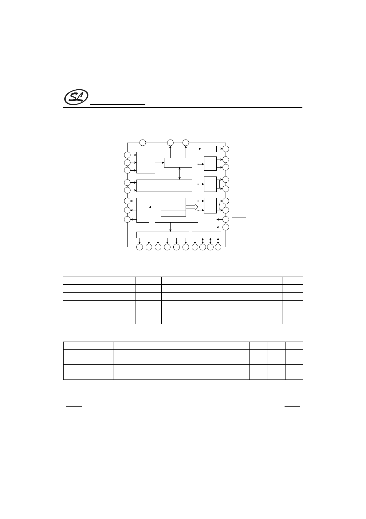
BLOCK DIAGRAM
HOLD
DO1 DO2
SC9318-033
X
OUT
X
V
FM
AM
COM1
COM2
COM3
IN
XT
IN
IN
Timing
Gene.
Programmable Counter
LCD
COM
S1 S23 K0 K3 T0 T3
Phase Comp
ROM
ALU
RAM
LCD Segment
MUTE MUTE
I/O
3
AD
2
I/O
I/O
1
Doubler
VEEC2 C1 V
LCD
P3-1/BUZR
P3-0
P2-3
P2-0
P1-3
P1-0
RESET
TEST
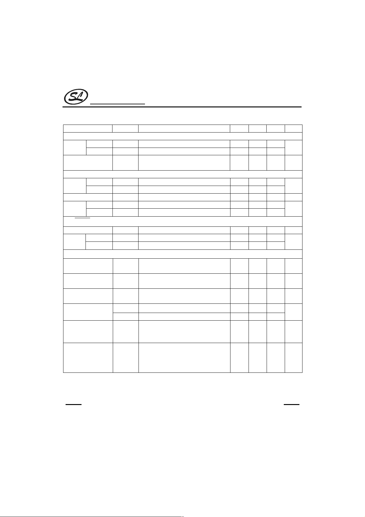
ABSOLUTE MAXIMUM RATING
Characteristic Symbol Value Unit
Supply Voltage VDD 1.3 V
Input Voltage VIN -0.3~ VDD+0.3 V
Power Dissipation PD 100 mW
Operating Temperature T
Storage Temperature T
-10~60
opr
-55~125
stg
°C
°C
ELECTRICAL CHARACTERISTICS
Characteristic Symbol Test Condition MIN TYP MAX Unit
Range of Operating
Supply Voltage
Range of Memory
Retention Voltage
V
* 1.8 3.0 3.6 V
DD
V
* Crystal oscillation stopped (CKSTP
HD
instruction executed)
HANGZHOU SILAN MICROELECTRONICS JOINT-STOCK CO.,LTD
(Tamb=25°C, VDD =3.0V, unless otherwise specified)
1.0 -- 3.6 mA
(To be continued)
3
Rev: 1.0 2002-01-16

Silan
Semiconductors
(Continued)
Characteristic Symbol Test Condition MIN TYP MAX Unit
Under ordinary operation and
PLL on operation, on output
I
DD1
Operating Current
I
DD2
I
DD3
I
DD4
Memory Retention
Current
Crystal Oscillation
Frequency
Crystal Oscillation
Startup Time
Voltage Doubler Circuit
Voltage Doubler
Reference Voltage
Constant Voltage
Temperature
Characteristics
Voltage Doubler
Boosting Voltage
Operating frequency ranges for programmable counter and IF counter
FMIN (VHF Mode) f
FMIN (FM Mode) fFM Sine wave input when VIN =0.2Vp-p 40 ~ 130
AMIN (HF Mode) fHL Sine wave input when VIN =0.2Vp-p 1 ~ 45
AMIN (LF Mode) fLF Sine wave input when VIN =0.2Vp-p 0.5 ~ 12
IFIN f
Input Amplitude VIN F
V
I
f
t
V
D
LCD
VHF
load FM
Under ordinary operation and
PLL on operation, no output
load F
Under CPU operation only
(PLL off, display turned on)
Soft wait mode (crystal oscillator, display
circuit operating, CPU stopped, PLL off)
Hard wait mode (crystal oscillator
operating only)
Crystal oscillation stopped (CKSTP
HD
instruction executed)
* -- 75 -- kHz
XT
Crystal oscillation fXT=75kHz -- -- 1.0 s
ST
GND reference (VEE) 1.3 1.5 1.7 V
EE
GND reference (VEE) -- -5 --
V
GND reference (V
Sine wave input when VIN =0.2Vp-p 50 ~ 230
Sine wave input when VIN =0.2Vp-p 0.35 ~ 12
IF
MIN
MIN
, A
=230MHz input
IN
=130MHz input
) 2.6 3.0 3.4 V
LCD
, I
input 0.2 ~
MIN
FIN
V
-- 6.0 10
-- 40 80
SC9318-033
=3V -- 7.0 12
DD
-- 25 50
-- 15 30
-- 0.1 10
V
DD
-0.8
(To be continued)
µA
mV/°
C
MHz
Vp-p
HANGZHOU SILAN MICROELECTRONICS JOINT-STOCK CO.,LTD
4
Rev: 1.0 2002-01-16
Silan
Semiconductors
(Continued)
Characteristic Symbol Test Condition MIN TYP MAX Unit
LCD common output/segment output (COM1~COM3, S1~S23)
“H” Level I
Current
“L” Level I
Output Voltage 1/2
Level
input port
HOLD
In put Leak Current ILI VIH=3.0V, VIL=0V -- -- ±1.0 µA
“H” Level V
Voltage
“L” Level V
A/D (N) converter (A/DIN2, DC-REF)
Analog Input
Voltage Range
Analog Reference
Voltage Range
Resolution V
Conversion Total
Error
Analog Input Leak ILI
KEY input port (K0~K3)
N-ch/P-ch Input
Resistance
“H” Level V
Voltage
“L” Level V
“H” Level V
Voltage
“L” Level V
Input Leak Current
Timing output port (T0~T5)
“H” Level I
Current
“L” Level I
N-ch Load
Resistance
V
OH1
V
OL1
V
No load 1.3 1.5 1.7 V
BS
-- 2.4 ~ 3.0 Input
IH1
-- 0 ~ 1.2
IL1
V
AD
AD
V
DC-REF, VDD =2.0~3.6V 1.0 ~
REF
-- -- 6.0 -- bit
RES
-- V
R
-- 75 150 300 kΩ
IN1
When input with pull-down resistance 1.8 ~ 3.0 Input
IH2
When input with pull-down resistance 0 ~ 0.3
IL2
When input with pull-up resistance 2.7 ~ 3.0 Input
IH3
When input with pull-up resistance 0 ~ 1.2
IL3
I
LI
VOH =2.7V -0.5 -1.0 -- Output
OH1
VOL=0.3V,Use LCD key-return mode 0.5 1.0 --
OL1
I
No used LCD key-return mode 75 150 300 kΩ
TL
=3V, VOH=2.7V -0.5 -1.0 -- Output
LCD
=3V, VOH =0.3V 0.5 1.0 --
LCD
, AD
IN1
=2.0~3.6V -- ±1.0 ±4.0 LSB
DD
=3.0V, VIL=0V
V
IH
(AD
IN1
0 ~ V
IN2
, AD
, DC-REF)
IN2
When input resistance off,
=3.0V, VIL=0V
V
IH
SC9318-033
V
DD
V
DD
×0.9
-- -- ±1.0 µA
-- -- ±1.0 µA
mA
V
V
V
V
mA
(To be continued)
HANGZHOU SILAN MICROELECTRONICS JOINT-STOCK CO.,LTD
5
Rev: 1.0 2002-01-16
Silan
Semiconductors
(Continued)
Characteristic Symbol Test Condition MIN TYP MAX Unit
DO1/OT, DO2 output; MUTE output
“H” Level I
Current
Output Off Leak
Current
General-purpose I/O ports (P1-0~P3-1)
Current
Input Leak Current ILI VIH=3.0V, VIL=0V -- --
Voltage
IN,
Input Leak Current ILI VIH=3.0V, VIL=0V -- --
Voltage
Others
Input Pull-Down
Resistance
XIN Amp Feedback
Resistance
X
OUT
Resistance
Resistance
Voltage Used to
Detect Supply
Voltage Drop
Supply Voltage Drop
Detection
Temperature
Characteristics
RESET
Output
“L” Level I
“H” Level I
“L” Level I
“H” Level V
“L” Level V
input port
“H” Level V
“L” Level V
VOH =2.7V -0.5 -1.0 -- Output
OH1
VOL =0.3V 0.5 1.0 --
OL1
=3.0V, V
V
TLH
I
TL
(DO1, DO2)
VOH =2.7V -0.5 -1.0 -- Output
OH1
VOL =0.3V 0.5 1.0 --
OL1
-- 2.4 ~ 3.0 Input
IH4
-- 0 ~ 0.6
IL4
-- 2.4 ~ 3.0 Input
IH4
-- 0 ~ 0.6
IL4
R
(TEST) 25 50 100
IN2
R
(XIN-X
fXT
R
(X
OUT
R
(F
fIN1
R
(I
fIN2
V
VDD 1.3 1.5 1.6 V
STP
DS V
OUT
) -- 3 --
OUT
, A
MIN
500 1000 2000
FIN)
-- -2 --
DD
=0V
TLL
) -- 20 --
) 150 300 600 Input Amp Feedback
MIN
HANGZHOU SILAN MICROELECTRONICS JOINT-STOCK CO.,LTD
6
SC9318-033
-- --
±100
±1.0 µA
±1.0 µA
Rev: 1.0 2002-01-16
mA
nA
mA
V
V
kΩ
MΩ
kΩ
kΩ
mV/°C
Silan
Semiconductors
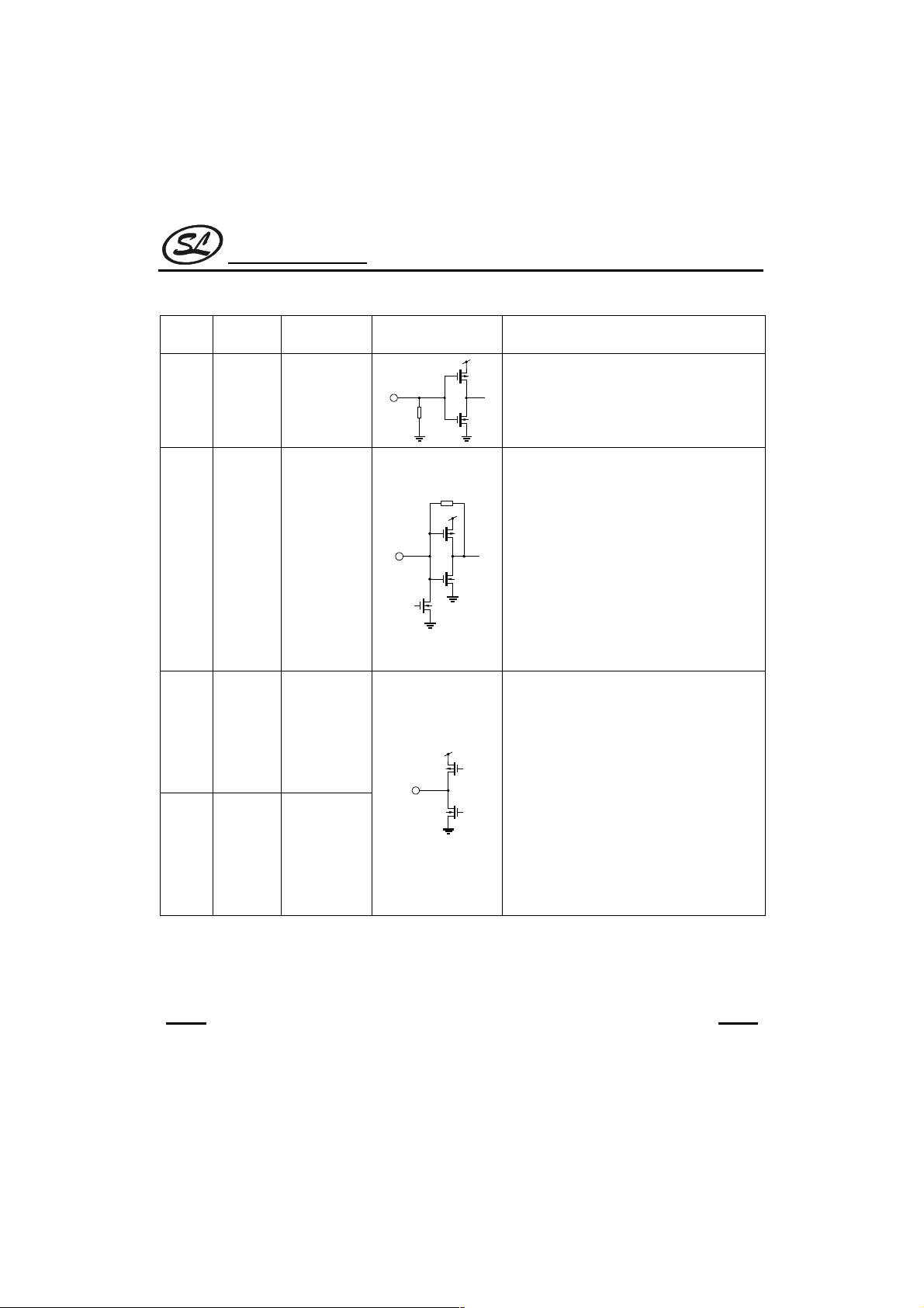
PIN DESCRIPTION
Pin
No.
4~18 S1~S15
19~26
27~30 K0~K3
Symbol Pin Name
1 COM1
2 COM2
3 COM3
S16/KR7
~
S23/KR0
LCD common
LCD segment
LCD segment
output
output
output/Key
return timing
output
Key input
ports
Internal
Connection
V
LCD
V
LCD
RIN1RIN1
SC9318-033
Description
Output common signal to the LCD panel.
Through a matrix with pins S1~S23, a
maximum of 69 segments can be displayed.
Three levels, V
V
EE
at 83Hz every 2ms. V
SYSTEM RESET and CLOCK STOP are
released, and a common signal is output after
the DISP OFF bit is set to “0”.
Segment signal output pins for the LCD panel.
Together with COM1, COM2, and COM3, a
matrix is formed that can display a maximum of
69 segments. The signals for the key matrix
and the segment signals from pins
S16/KR7~S23/KR0 are output on a time
division basis. 4 X 8=32 key matrix can be
created in conjunction with key input ports
K0~K3.
4 bit input ports for key matrix input. Combined
in a matrix with key return timing outputs the
LCD segment pins, data from a maximum of
4X8=32 keys can be input and pins are pulled
up. On the key setting output pin, data from
4X6=24 keys can be input and pins are pulled
down. The WAIT mode is released when high
level is applied to key input ports set to pull-
down.
, VEE, and GND, are output
LCD
EE
is output after
31~36 T0~T5
HANGZHOU SILAN MICROELECTRONICS JOINT-STOCK CO.,LTD
Key return
timing output
port
These ports output the timing signal for key
matrix. To form the key matrix, load resistance
RON
has been built-in the N-channel side. When the
key matrix combined with push-key that does
not need a key matrix diode.
(To be continued)
7
Rev: 1.0 2002-01-16
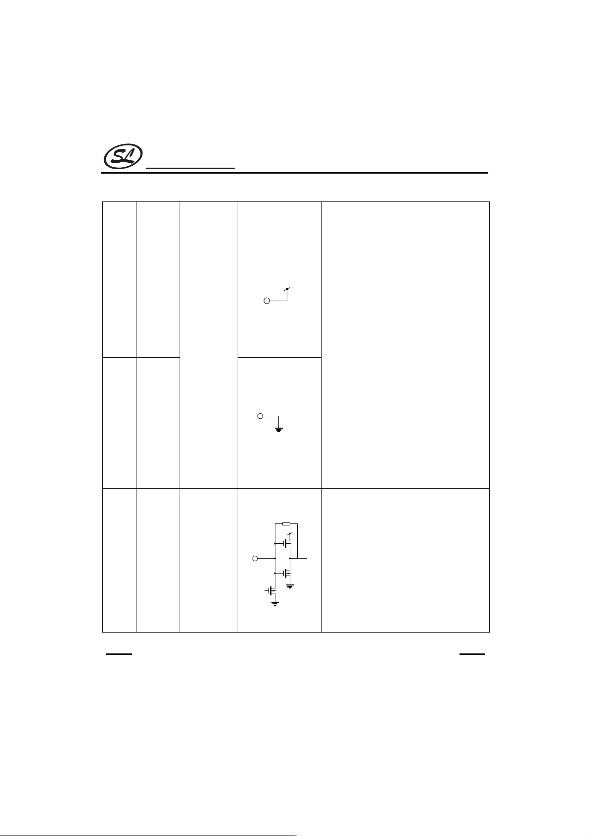
(Continued)
Pin
No.
37~40
41~44
45~46
Silan
Semiconductors
Symbol Pin Name
P1-0
~
P1-3
P2-0
P2-1/
AD
IN1
P2-2/
AD
IN2
P2-3/
DC-REF
P3-0
P3-1/
BUZR
I/O port 1
I/O port 2
/AD analog
voltage input
/AD analog
voltage input
/Reference
voltage input
I/O port 3
/Buzzer
output
Internal
Connection
To A/D converter
(P2-0 pin is excluded)
SC9318-033
Description
The input and output of these 4 bit I/O ports
can be programmed in 1 bit units. By altering
the input to I/O ports set to input, the CLOCK
STOP and WAIT modes can be released, and
the MUTE bit of the MUTE pin can be set to
“1”.
4 bit I/O ports.
Input and output may be programmed in 1 bit
units. Pins P2-1 through P2-2 can also be used
for analog input to the built-in 6 bit, 2-channel
A/D converter.
Conversion time of the built-in A/D converter
using the successive comparison method is
280µs. The necessary pin can be programmed
to A/D analog input in 1 bit units, and P2-3 can
be set to the reference voltage input. Internal
power supply (V
can be used as the reference voltage. In
addition, constant voltage (V
the A/D analog input so battery voltage, etc.,
can be easily detected. The reference voltage
input, for which a built-in operational amp is
used, has high impedance.
The A/D converter, and their control are all
executed by program.
2 bit I/O ports, whose input/output can be
programmed in 1 bit units.
The P3-1 pin also functions as the output for
the built-in buzzer circuit. The buzzer sound
can be output in 254 different tones between
18.75kHz and 147Hz, and at a duty of 50%.
The buzzer output, and all associated controls
can be programmed.
) or constant voltage (VEE)
DD
) can be input to
EE
(To be continued)
HANGZHOU SILAN MICROELECTRONICS JOINT-STOCK CO.,LTD
8
Rev: 1.0 2002-01-16
(Continued)
Pin
No.
47 MUTE
49
Silan
Semiconductors
Symbol Pin Name
Muting output
port
HOLD mode
HOLD
control input
Internal
Connection
SC9318-033
Description
1 bit output port. Normally, this port is used for
muting control signal output. This pin can set
the internal MUTE bit to “1” according to a
change in the input of I/O port 1. MUTE bit
output logic can be changed; PLL phase
difference can also be output using this pin.
Input pin for request/release HOLD mode.
Normally, this pin is used to input radio mode
selection signals or battery detection signals.
HOLD mode includes CLOCK STOP mode
(stops crystal oscillation) and WAIT mode
(halts CPU). Setting is implemented with the
CKSTP instruction or the WAIT instruction.
When the CKSTP instruction is executed,
request/release of the HOLD mode depends on
the internal MODE bit. If the MODE bit is “0”
(MODE-0), executing the CKSTP instruction
while the
clock generator and the CPU and changes to
memory back-up mode. If the MODE bit is “1”
(MODE-1), executing the CKSTP instruction
enters memory back-up mode regardless of the
level of the
release when the
MODE-0, or when the level of the
low in MODE-1.
When memory back-up mode is entered by
executing a WAIT instruction, any change in
the
HOLD
In memory back-up mode, current consumption
is low (below 10µA), and all the output pins
(e.g., display output, output ports) are
automatically set to low level.
pin is at low level stops the
HOLD
pin. Memory back-up is
HOLD
pin goes high in
HOLD
pin input releases the mode.
(To be continued)
HOLD
pin
HANGZHOU SILAN MICROELECTRONICS JOINT-STOCK CO.,LTD
9
Rev: 1.0 2002-01-16
(Continued)
Pin
No.
48 TEST
50 IFIN/IN
51
52 DO2
Silan
Semiconductors
Symbol Pin Name
TEST mode
control input
IF signal
input/Input
port
Phase
DO1/OT
comparison
output /Output
port
Phase
comparison
output
Internal
Connection
RIN2
R
fIN2
SC9318-033
Description
Input pin used for controlling TEST mode. High
level indicates TEST mode, while low level
indicates normal operation. The pin is normally
used at low level or no-connection (NC). (A
pull-down resistor is built-in).
IF counter’s IF signal input for counting the IF
signals of the FM and AM bands and detecting
the automatic stop position.
The input frequency is between 0.35~12MHz
(Min)). A built-in input amp and C
(0.2V
P-P
coupling allow operation at low-level input.
The IF counter is a 20 bit counter with optional
gate times of 1, 4, 16, and 64ms. 20 bit of data
can be readily stored in memory.
This input pin can be programmed for use as
an input port (IN port). CMOS input is used
when the pin is set as an IN port.
PLL’s phase comparison tri-state output pins.
When the programmable counter’s prescaler
output is higher than the reference frequency,
output is at high level. When output is lower
than the reference frequency, high impedance
output is obtained.
Because DO1 and DO2 are output in parallel,
optimal filter constants can be designed for the
FM/VHF and AM bands. Pin DO1 can be
programmed to high impedance or
programmed as an output port (OT). Thus the
pins can be used to improve lock-up time or
used as output ports.
(To be continued)
HANGZHOU SILAN MICROELECTRONICS JOINT-STOCK CO.,LTD
Rev: 1.0 2002-01-16
10
(Continued)
Pin
No.
56 VDD
53 GND
54 FMIN
HANGZHOU SILAN MICROELECTRONICS JOINT-STOCK CO.,LTD
Silan
Semiconductors
Symbol Pin Name
Power-supply
pins
FM
programmabl
e counter
input
Internal
Connection
V
DD
GND
R
fIN2
11
SC9318-033
Description
Pins to which power is applied.
Normally, V
In back-up mode (when CKSTP instructions
are being executed), voltage can be lowered to
1.0V. If voltage falls below 1.5V while the CPU
is operating, the CPU stops to prevent
malfunction (STOP mode). When the voltage
rises above 1.5V, the CPU restarts.
STOP mode can be detected by checking the
STOP F/F bit. If necessary, execute
initialization or adjust clock by program.
When detecting or preventing CPU
malfunctions using an external circuit, STOP
mode can be invalidated and rendered non-
operative by program. In that case, all four bits
of the internal TEST port should be set to “1”.
If more than 1.8V is applied when the pin
voltage is 0, the device’s system is reset and
the program starts from address “0”. (power on
reset).(Note)
To operate the power on reset, the power
supply should start up in 10~100ms.
Programmable counter input pin for FM,VHF
band.
The 1/2+pulse swallow system (VHF mode)
and the pulse swallow system (FM mode) are
selectable freely by program. At the VHF mode,
local oscillation output (VCO output) of
50~230MHz (0.2V
mode, 40~130MHz (0.2V
built-in input amp and C coupling allow
operation at low-level input. (Note) when in the
PLL OFF mode or when set to AM
input is pulled down.
=1.8~3.6V (3.0V Typ.) is applied.
DD
(Min)) is input and FM
P-P
(Min)) is input. A
P-P
input, the
IN
(To be continued)
Rev: 1.0 2002-01-16
 Loading...