

Silan
Semiconductors
SC9270C/D
HANGZHOU SILAN MICROELECTRONICS JOINT-STOCK CO.,LTD
Rev: 1.1 2001.04.27
1
DTMF RECEIVER
DESCRIPTION
The SC9270C/D is a complete DTMF receiver integrating both
the bandsplit filter and digital decoder functions. The filter section
uses switched capacitor techniques for high- and low-group filters
and dial-tone rejection. Digital counting techniques are employed in
the decoder to detect and decode all 16 DTMF tone-pairs into a 4-bit
code. External component count is minimized by on-chip provision of
a differential input amplifier, clock-oscillator and latched 3-state bus
interface.
FEATURES
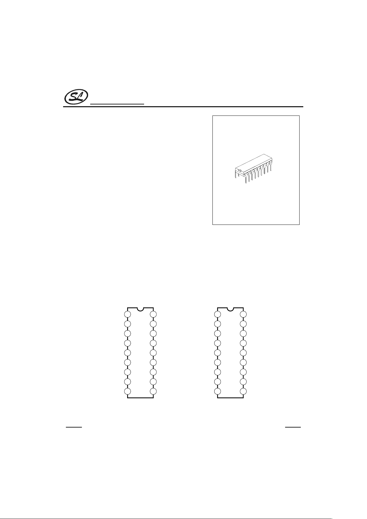
*Complete receiver in an 18-pin package
*Excellent performance
*CMOS, single 5 volt operation,
*Widely operating voltage: 1.2V ~ 5.25V
*Minimum board area
*Central office quality
*Low power consumption
*Power-Downmode (SC9270D only)
*Inhibit-mode (SC9270D only)
DIP-18
APPLICATIONS
*Paging systems
*Repeater systems / Mobile radio
*Credit card systems
*Remote control
*Personal computers
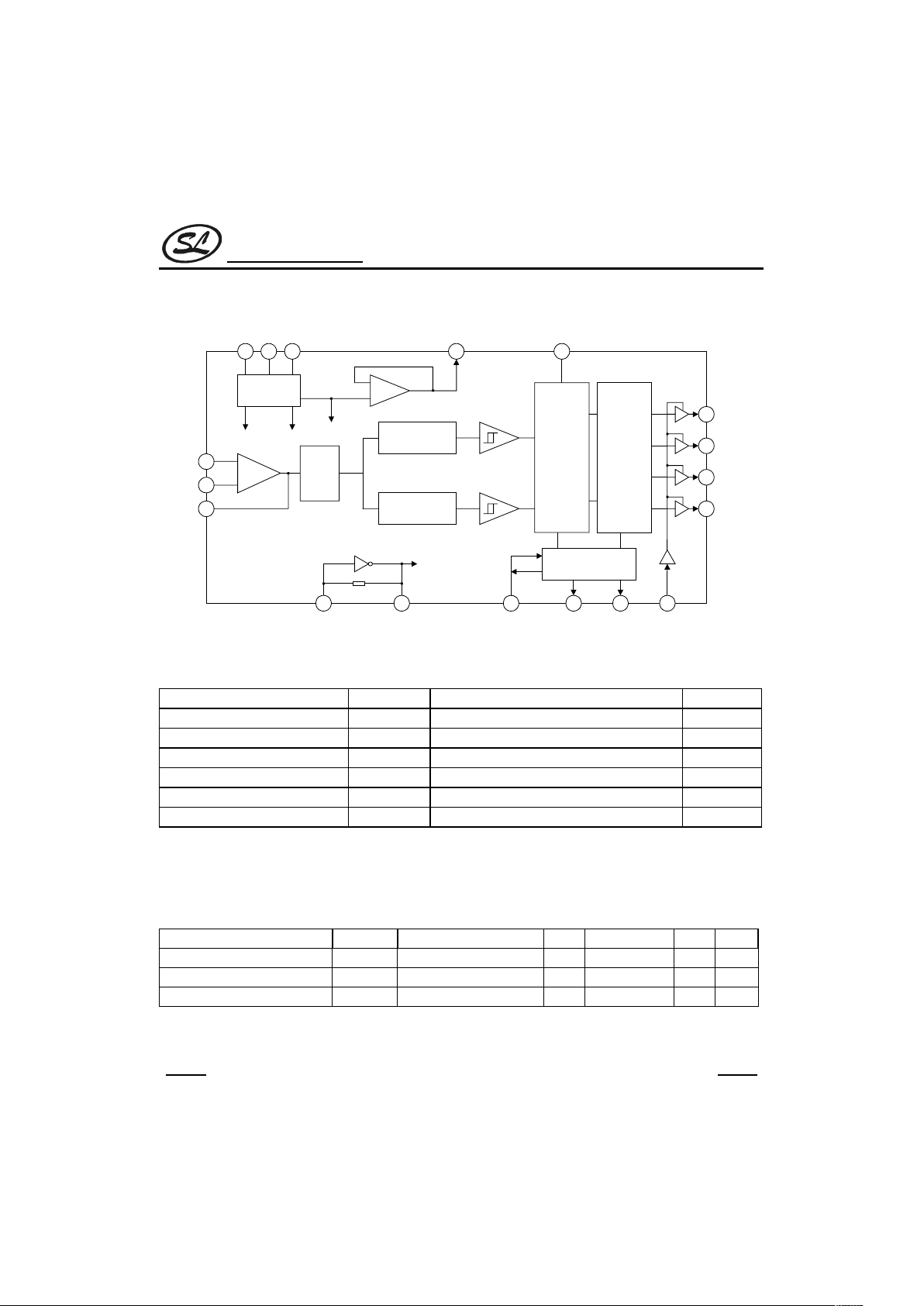
PIN CONFIGURATIONS
1
2
3
4
5
6
7
8
SC9270C
IN+
IN-
GS
VREF
IC*
IC*
OSCI
OSCO Q1
16
15
14
13
12
11
10
VDD
St/GT
ESt
StD
Q4
Q3
Q2
9
18
17
VSS TOE
* Connect to V
SS
1
2
3
4
5
6
7
8
SC9270D
IN+
IN-
GS
VREF
INH
PWDN
OSCI
OSCO Q1
16
15
14
13
12
11
10
VDD
St/GT
ESt
StD
Q4
Q3
Q2
9
18
17
VSS TOE
Silan
Semiconductors
SC9270C/D
HANGZHOU SILAN MICROELECTRONICS JOINT-STOCK CO.,LTD
Rev: 1.1 2001.04.27
2
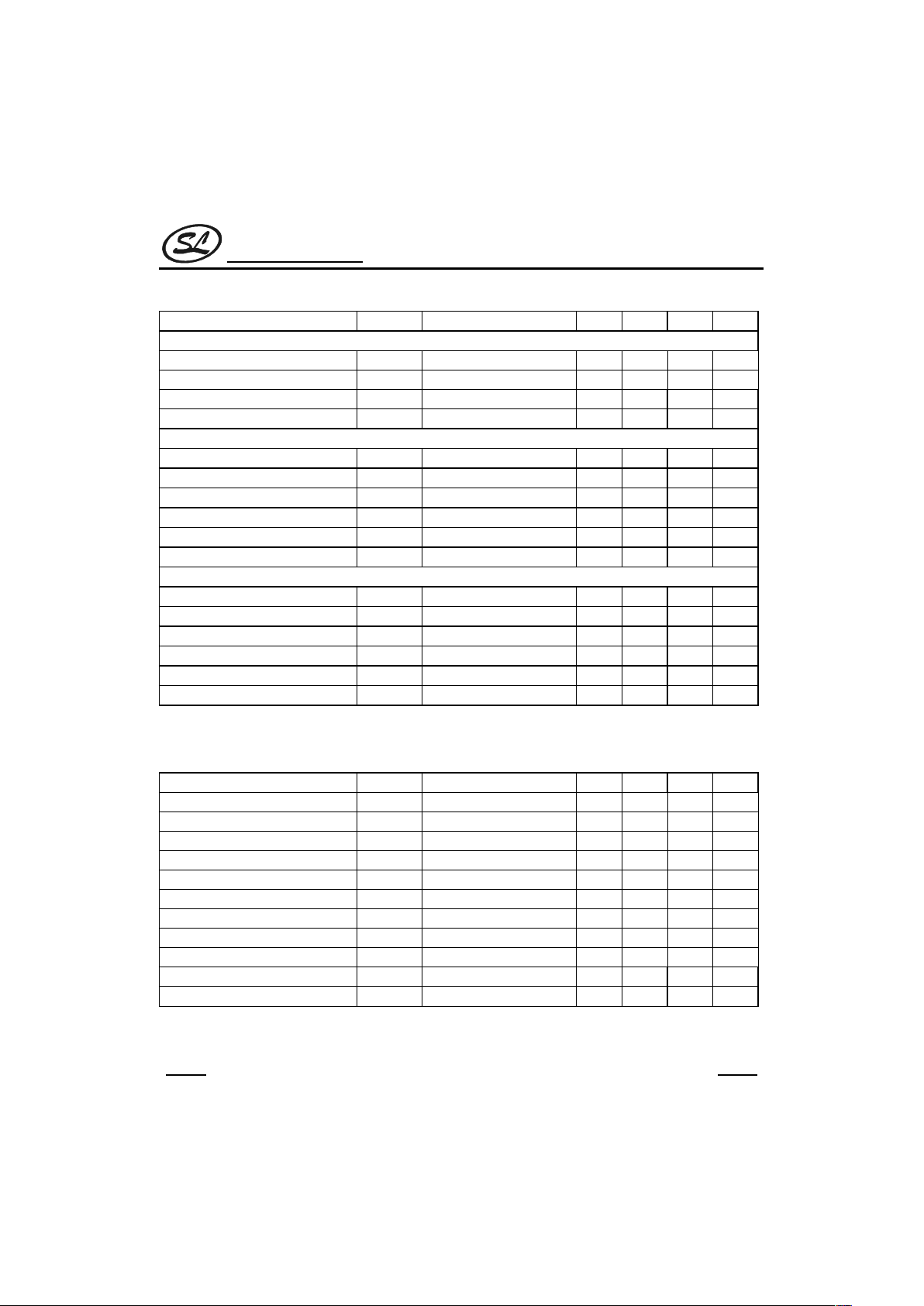
BLOCK DIAGRAM
BIAS
CIRCUIT
18 9 6
Chip power Chip bias
1
2
DIAL
TONE
FILTER
3
5
HIGH GROUP
FILTER
HIGH GROUP
FILTER
DIGITAL
DETECTION
ALGORITHM
CODE
CONVERTER
AND
LATCH
11
12
13
14
STEERING
LOGIC
16 151787 10
St
GT
Chip clock
Chip ref
Zero crossingdetectors
-
+
+
-
IN+
GS
IN-
V
DDVSS
PWDN V
REF
Q1
Q2
Q3
Q4
TOEStDEStSt/GTOSCOOSCI
4
INH
Figure 1. block diagram
ABSOLUTE MAXIMUM RATINGS
(Notes 1, 2, 3)
Characteristic Symbol Value Unit
Power Supply Voltage VDD-V
SS
6V
Voltage on any pin -- VSS-0.3 ~ VDD+0.3 V
Current at any pin -- 10 mA
Operating temperature Topr -40~+85
°C
Storage Temperature Tstg -65~+150
°C
Package power dissipation 500 mW
Note: 1. Absolute maximum ratings are those values beyond which damage to the device may occur.
2. Unless otherwisespecified, all voltages are referenced to ground.
3. Power dissipation temperature derating: -12 mV / from 65°C to 85°C
RECOMMENDED OPERATING CONDITIONS
(Note 1)
Parameter Symbol Conditions Min Typ(Note 2) Max Unit
Positive SupplyVoltages V
DD
VSS=0V 1.2 5 -- V
Oscillator Clock Frequency fc -- -- 3.579545 -- MHz
Oscillator Frequency Tolerance
∆fc
-- --
±0.1
-- %
Note: 1. Voltages are with respect to ground(Vss), unless otherwise stated.
2 .Typical figures are at 25°C and are for design aid only: not guaranteedandnot subject to production testing.
Silan
Semiconductors
SC9270C/D
HANGZHOU SILAN MICROELECTRONICS JOINT-STOCK CO.,LTD
Rev: 1.1 2001.04.27
3
DC ELECTRICAL CHARACTERISTICS
Parameter Symbol Conditions Min Typ Max Unit
SUPPLY
Operating Supply Voltage V
DD
-- 1.2 -- 5.25 V
Operating Supply Current I
CC
-- -- 3.0 7.0 mA
Power Consumption P
O
f=3.579MHz; VDD=5V -- 15 35 mW
Standby Current I
S
PWDN pin = V
DD
-- -- 100
µA
INPUTS
Low Level Input Voltage V
IL
-- -- -- 1.5 V
High Level Input Voltage V
IH
-- 3.5----V
Input Leakage Current IIH/IILVIN=VSSor V
DD
-- 0.1 --
µA
Pull up(Source) Current I
SO
TOE(Pin 10)=0V -- 7.5 15
µA
Input Impedance (IN+, IN-) R
IN
@1kHz -- 10 --
MΩ
Steering Threshold Voltage V
TSt
-- -- 2.35 -- V
OUTPUTS
Low Level Output Voltage V
OL
No load -- 0.03 -- V
High Level Output Voltage V
OH
No load -- 4.97 --
µA
Output Low(Sink) Current I
OL
V
OUT
=0.4V 1.0 2.5 -- mA
Output High(Source) Current I
OH
V
OUT
=4.6V 0.4 0.8 -- mA
V
REF
Output Voltage V
REF
No load 2.4 -- 2.7 V
V
REF
Output Resistance R
OR
-- -- 10 --
kΩ
OPERATING CHARACTERISTICS
Gain Setting Amplifier
Parameter Symbol Conditions Min Typ Max Unit
Input Leakage Current I
IN
VSS<VIN<V
DD
--
±100
-- nA
Input Resistance R
IN
-- -- 10 --
MΩ
Input Offset Voltage V
OS
-- --
±25
-- mV
Power Supply Rejection PSRR 1kHz -- 60 -- dB
Common Mode Rejection CMRR -3.0V < VIN<3.0V --60--dB
DC Open Loop Voltage Gain A
VOL
-- -- 65 -- dB
Open Loop UnityGain Bandwidth f
C
-- -- 1.5 -- MHz
Output Voltage Sw ing V
O
RL≥100kΩ to V
SS -- 4.5 -- V
PP
Tolerable capacitive load(GS) C
L
-- -- 100 -- PF
Tolerable resistive load(GS) R
L
-- -- 50 --
kΩ
Common Mode Range V
CM
No load -- 3.0 -- V
PP
Notes : 1. All voltages referenced to VDD unless otherwise noted.
2. V
DD
=5.0V,VSS=0V,TA= 25°C .
Silan
Semiconductors
SC9270C/D
HANGZHOU SILAN MICROELECTRONICS JOINT-STOCK CO.,LTD
Rev: 1.1 2001.04.27
4
AC CHARACTERISTICS
(All voltage referenced to Vss otherwise noted; VDD=5.0V, VSS=0V, TA=25°C,
f
CLK
=3.579545 MHz, using test circuit of figure 2 & 3. Typical figures areat 25°C and are for design aid only: not
guaranteed and not subject to production testing)
Parameter
Symbo
l
Test Conditions Min Typ Max Unit
SIGNAL CONDITIONS
-- Note:1,2,3,5,6,9,11 -- -- -40 dBm
-- Note:1,2,3,5,6,9,11 -- -- 7.75 mV
RMS
-- Note:1,2,3,5,6,9,11 +1 -- -- dBm
Valid Input Signal Levels
(each tone of composite signal)
-- Note:1,2,3,5,6,9,11 883 -- -- mV
RMS
Positive Twist Accept -- Note:2,3,6,9,11 -- 10 -- dB
Negative Twist Accept -- Note:2,3,6,9,11 -- 10 -- dB
Frequency Deviation Accept Limit -- Note:2,3,5,9,11 --
±1.5%±2Hz
-Frequency Deviation Reject Limit -- Note:2,3,5,11 ±3.5 -- -Thrid Tone Tolerance -- Note:2,3,4,5,9,13 -18.5 -- dB
Noise Tolerance -- Note:2,3,4,5,7,9,10 -- -12 dB
Dial Tone Tolerance -- Note:2,3,4,5,8,9,11 -- +18 -- dB
TIMING
Tone Present Detection Time tDPRefer to Fig. 4. Note:12 5 14 16 ms
Tone Absent Detection Time tDARefer to Fig. 4. Note:12 0.5 4 8.5 ms
Tone Duration Accept t
REC
User adjustable -- -- 40 ms
Tone Duration Reject t
REC
User adjustable 20 -- -- ms
Interdigit Pause Accept tIDUser adjustable -- -- 40 ms
Interdigit Pause Reject t
DO
User adjustable 20 -- -- ms
OUTPUTS
Propagation Delay (St to Q) t
PQ
TOE=V
DD
-- 8 11
µs
Propagation Delay (St to StD) t
PSED
TOE=V
DD
-- 12 --
µs
Output Data Set Up (Q to Std) t
QSED
TOE=V
DD
-- 4.5 --
µs
Propagation Delay (TOE to Q Enable) t
PTE
RL=10kΩ,CL=50pf
-- 50 -- ns
Propagation Delay (TOE to Q Disable) t
PTD
RL=10kΩ,CL=50pf
-- 300 -- ns
CLOCK
Crystal/Clock Frequency fC-- 3.5759 3.5759 3.581 MHz
Clock Input Rise Time t
LHCL
Ext. clock -- -- 110 ns
Clock Input Fall Time t
HLCL
Ext. clock -- -- 110 ns
Clock Input Duty Time DCCLExt. clock 40 50 60 %
Capacitive Load (OSCO) CLO-- -- -- 30 pf
Notes: 1. dBm = decibels above or below a reference power of 1mW into a 600 Ohm load.
2. Digit sequences consists of all 16 DTMF tones.
 Loading...