

Silan
A
Semiconductors
PLL FOR DTS
DESCRIPTION
The SC9256 is phase-locked loop (PLL) LSIs for digital tuning
systems (DTS) with built in2 modulus prescalers.
ll functions ate controlled through 3 serial bus lines. These LSIs
are used to configure high-performance digital tuning system.
FEATURES
* Optimal for configuring digital tuning systems in high-fi tuners
and car stereos.
* built-in prescalers. Operate at input frequency ranging from
30~150 MHz during FM
at 0.5~40MHz during AM
direct dividing).
* 16 bit programmable counter, dual parallel output phase
comparator, crystal oscillator and reference counter.
* 3.6MHz, 4.5MHz, 7.2MHz or 10.8MHz crystal oscillators can be
used.
* 15 possible reference frequencies. ( When using 4.5MHz crystal)
* Built-in 20 bit general-purpose counter for such uses as
measuring intermediate frequencies (IF
* High-precision (±0.55~±7.15µs) PLL phase error detection.
* Numerous general-purpose I/O pins for such uses as peripheral
circuit control.
* 3 N-channel open-drain output ports (OFF withstanding
voltage:12V) for such uses as control signal output.
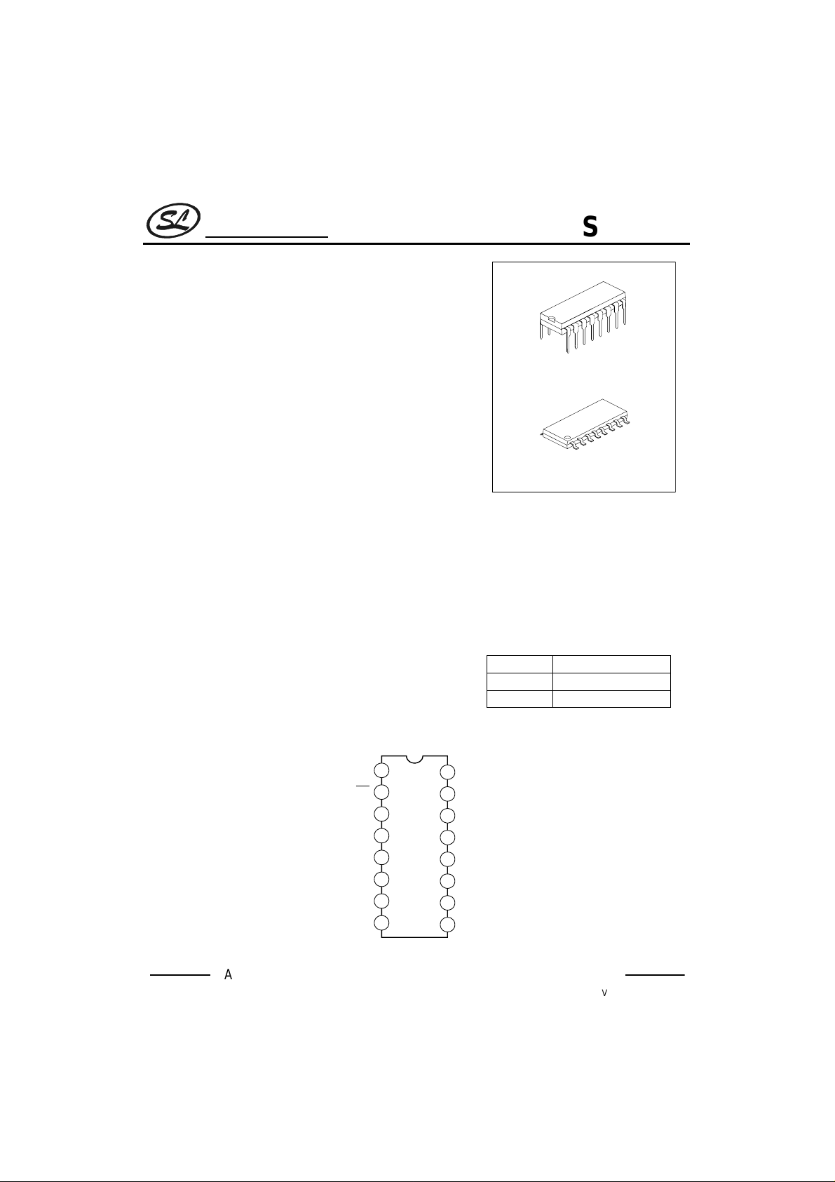
PIN CONFIGURATION
input (with 2 modulus prescaler) and
IN
input (with 2 modulus prescaler or
IN
IN1
and IF
IN2
)
SC9256
DIP-16-300-2.54
SOP-16-300-1.27
* Standby mode function (turns off FM, AM
and IF amps) to save current
consumption.
* All functions controlled through 3 serial
bus lines.
* CMOS structure with operating power
supply range of V
ORDERING INFORMATION
Device Package
SC9256 DIP-16-300-2.54
SC9256S SOP-16-300-1.27
=5.0±0.5V.
DD
1
XT
2
XT
DATA
OT-1
OT-2
OT-3
3
4
5
6
7
8
SC9256
PERIOD
CLOCK
HANGZHOU SILAN MICROELECTRONICS JOINT-STOCK CO.,LTD
16
15
14
13
12
11
10
9
DO2/OT-4
DO1
IN1
I/O-5/IF
I/O-6/IF
IN2
GND
FM
IN
AM
IN
V
DD
REV: 1.0 2002.01.30.
1
Silan
Semiconductors
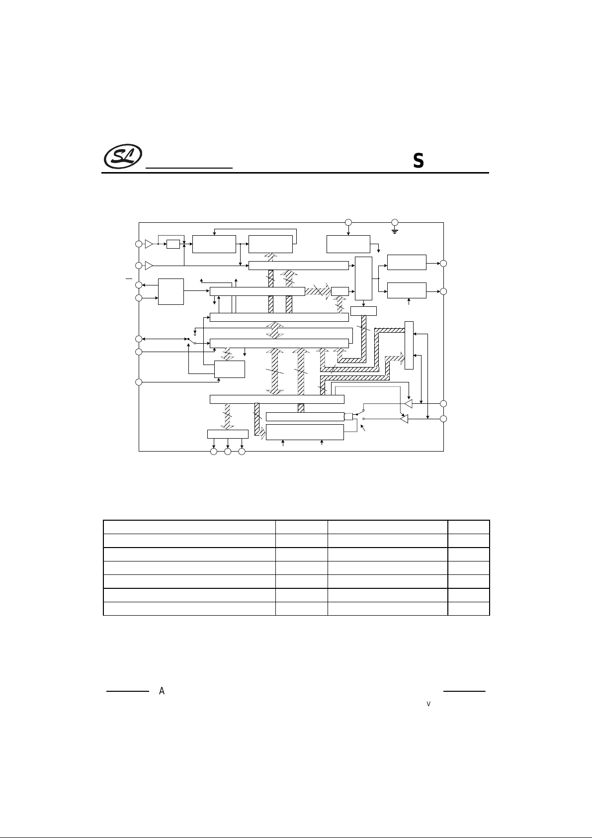
BLOCK DIAGRAM
FM
L
1/2
OSC
CIRCUIT
H
FM
AM
DATA
CLOCK
PERIOD
AMP
IN
IN
XT
XT
2 MODULUS
PERSCALER
HFFM
FM
1ms
OUTPUT PORT
OT-1 OT-2 OT-3
PSC
4bit SWALLOW
COUNTER
12bit PROGRAMMABLE COUNTER
LF
MODE
4
REFERENCE COUNTER MAX
OSC
24bit REGISTER
24bit SHIFT REGISTER
8
4
TEST
24bit REGISTER
4
ADDRESS
DECODER
12
15
24 22
10
20bit BINARY COUNTER
UNIVERSAL COUNTER
CONTROL
XT
1ms
V
DD
POWER ON
RESET
4
5
PHASE
UNLOCK
GATE
SC9256
GND
RESET
TRI-STATE
BUFFER
TRI-STATE
BUFFER
COMPARATOR
OT4
5
I/O PORT
AMP
AMP
DO1
DO2/OT-4
I/O-6/IF
I/O-5/IF
IN2
IN1
ABSOLUTE MAXIMUM RATINGS
Characteristic Symbol Value Unit
Supply Voltage V
Input Voltage V
N-ch Open-Drain Off withstanding Voltage V
PowerDissipation P
Operating Temperature T
Storage Temperature T
( ): Flat package
(Ta=25°C)
HANGZHOU SILAN MICROELECTRONICS JOINT-STOCK CO.,LTD
2
CC
IN
OFF
D
OPR
STG
-0.3~6.0 V
-0.3~VDD+0.3 V
13 V
300(200) mW
-40~85
-65~150
REV: 1.0 2002.01.30.
°C
°C
Silan
Semiconductors
ELECTRICAL CHARACTERISTICS
Characteristic Symbol Test Condition/Pin Min Typ. Max Unit
Operating Power Supply Voltage V
DD1
(unless otherwise specified, Ta= -40~85°C, VDD=4.5~5.58V.)
PLL operation
(normal operating)
4.5 5.0 5.5 V
SC9256
Operating Power Supply Current I
Stand-by mode
Crystal Oscillation Frequency
Supply Voltage
Operating Power Supply Current I
Operating Power Supply Current I
Operating frequency range
Crystal Oscillation Frequency f
FMIN(FMH,FML)f
FMIN(FML)f
AMIN(HF) f
AMIN(LF) f
IF
,IF
IN1
IN2
SC
IN
Operating input amplitude range
FMIN(FMH,FML)
FMIN(FML)V
AMIN(HF) V
AMIN(LF) V
IF
,IF
IN1
IN2
OT1~OT4 N-ch open drain
Output Current “L” level I
OFF-leak Current I
V
V
VDD=5.0V, XT=10.8MHz,
DD1
FMIN=150MHz
PLL OFF
(Operating crystal
DD2
oscillation)
VDD=5.0V, XT =10.8MHz
DD2
PLL OFF
VDD=5.0V, XT stop,
DD3
PLL OFF
Connect crystal resonator
XT
to XTFMH,FMLmode,
FM
V
IN
FMLmode, VIN=0.3Vp-p 30 ~ 150 MHz
FML
HF mode, VIN=0.2Vp-p 1 ~ 40 MHz
HF
LF mode, VIN=0.2Vp-p 0.5 ~ 20 MHz
LF
f
VIN=0.2Vp-p 0.1 ~ 15 MHz
IF
VIH=0.7VDD,VIL=0.3VDD,
f
SC
square wave input.
FMH,FMLmode,
FM
f
IN
FMLmode, fIN=30~150MHz 0.3 ~ VDD-0.5 Vp-p
FML
HF mode, fIN=1~40MHz 0.2 ~ VDD-0.5 Vp-p
HF
LF mode, fIN=0.5~20MHz 0.2 ~ VDD-0.5 Vp-p
LF
V
FIN=0.1~15MHz 0.2 ~ VDD-0.5 Vp-p
IF
VOL=1.0V 5.0 10.0 -- mA
OL1
V
OEF
OFF
terminal
XT
=0.2Vp-p
=30~130MHz
=12V -- --- 2.0
-- 7 15 mA
4.0 5.0 5.5 V
-- 0.8 1.5 mA
-- 120 240
3.6 ~ 10.8 MHz
30 ~ 130 MHz
-- ~ 100 kHz
0.2 ~ V
DD
(To be continued)
µA
-0.5 Vp-p
µA
HANGZHOU SILAN MICROELECTRONICS JOINT-STOCK CO.,LTD
REV: 1.0 2002.01.30.
3
Silan
Semiconductors
(Continued)
Characteristic Symbol Test Condition/Pin Min Typ. Max Unit
I/O-5~I/O-9, SC
Input Voltage
PERIOD, CLOCK, DATA
Input Voltage
DO1, DO2
Tri-State Lead Current I
XT
Input feedback resistance
Input Feedback
Resistance
IN
“H” level V
“L” level V
“H” level I
“L” level I
“H” level I
“L” level I
“H” level V
“L” level V
“H” level I
“L” level I
“H” level I
“L” level I
“H” level I
“L” level I
“H” level I
“L” level I
“H” level
“L” level Rf2
IH1
IL1
VIH=5V -- -- 2.0Input Current
IH
VIL=0V -- -- -2.0
IL
VOH=4.0V (expect SCIN) -2.0 -4.0 --Output Current
OH4
VOL=1.0V (expect SCIN)2.04.0--
OL4
IH2
IL2
VIH=5V -- -- 2.0Input Current
IH
VIL=0V -- -- -2.0
IL
VOH=4.0V (DATA) -1.0 -3.0 --Output Current
OH5
VOL=1.0V (DATA) 1.0 3.0 --
OL5
VOH=4.0V -2.0 -4.0 --Input Current
OH3
VOL=1.0V 2.0 4.0 --
OL3
V
TL
OH2
OL2
Rf1
=5V, V
TLH
VOH=4.0V -0.1 -0.3 --Output Current
VOL=1.0V 0.1 0.3 --
FMIN, AMIN, IFIN
(Ta=25°C)
XT-
XT
=0V -- --
TLL
(Ta=25°C)
0.7V
DD
0 ~ 0.3V
0.8V
DD
0 ~ 0.2V
350 700 1400
500 1000 4000
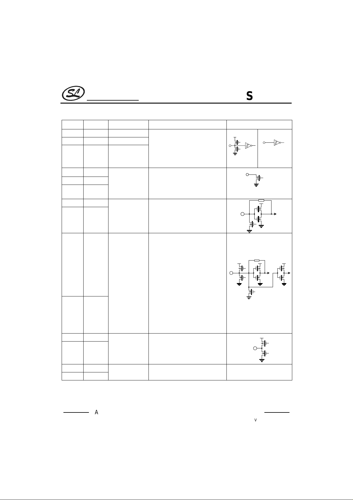
PIN DESCRIPTION
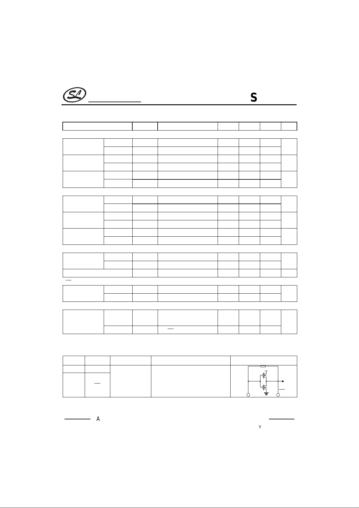
Pin No. Symbol Pin name Description Circuit diagram
1XT
Crystal oscillator
pins
2
XT
Connects 3.6MHz, 4.5MHz, 7.2MHz
or 10.8MHz crystal oscillator to
supply reference frequency and
internal clock
SC9256
~V
~V
XT XT
DD
DD
DD
DD
±1.0 µA
V
DD
V
µA
mA
V
µA
mA
mA
mA
kΩ
(To be continued)
HANGZHOU SILAN MICROELECTRONICS JOINT-STOCK CO.,LTD
REV: 1.0 2002.01.30.
4
Silan
Semiconductors
(Continued)
Pin No. Symbol Pin name Description Circuit diagram
3 PERIOD Period signal input
4 CLOCK Clock signal input
5DATA
6OT-1
7OT-2
8OT-3
10 AMIN
11 FMIN
13
14
15 DO1
16 DO2/OT-4
12 GND
9V
I/O-
6/IFIN2
I/O-5
/IFIN1
Serial data
input/output
General-purpose
output ports
Programmable
counter input
General-purpose
I/O ports/Generalpurpose counter
frequency
measurement
input
Phase comparator
output (Generalpurpose output
ports)
Power supply pins
DD
Serial I/O ports. These pins transfer
data to and from the controller to set
divisions and dividing modes, and to
control the general-purpose counter
and general-purpose I/O ports.
N channel open drain port pins, for
such uses as control signal output.
These pins are set to the OFF state
when power is turned on.
These pins input FM and AM band
local oscillator signals by capacitor
coupling. FM
low amplitude.
General-purpose I/O port input
/output pins. Can be switched for use
as input pins to measure general
purpose counter frequencies. The
frequency measurement function has
such uses as measuring intermediate frequencies (IF).
These pins feature built-in amps.
Data are input by capacitor coupling.
FM
IN
amplitude.
(note) Pins are set for input when
power is turned on.
These pins are for phase comparator
tri-state output. DO1 and DO2 are
output in parallel.
Applies 5.0V±10%
and AMINoperate at
IN
and AMINoperate at low
SC9256
V
DD
Schmitt
input
DATA
N-channel open drain
V
DD
V
DD
Schmitt input
CLOCK,PERIOD
VDD
HANGZHOU SILAN MICROELECTRONICS JOINT-STOCK CO.,LTD
REV: 1.0 2002.01.30.
5

Silan
Semiconductors
FUNCTION DESCRIPTION
Serial I/O ports
As the block diagram shows, the functions are controlled by setting data in the 48 bits contained in each of the 2
sets of 24 bit registers. Each bit of data in these register is transferred through the serial ports between the
controller and the DATA, CLOCK and PERIOD pins. Each serial transfer consists of a total of 32 bits, with 8
address bits and 24 data bits.
Since all functions are controlled in units of registers, the explanation in this manual focuses on the 8 bit address
and functions of each register.
These registers consist of 24 bits and are selected by an 8 bit address.
A list of the address assignment for each register is given below under register assignments.
Register Address Contents of 24 bits No. of bit
PLL divisor setting
Input
register 1
Input
register 2
Output
register 1
Output
register 2
D0H
D2H
D1H
D3H
Reference frequency setting
PLL input and mode setting
Crystal oscillator selection
General=purpose counter control (including lock detection bit
control)
I/O port and general-purpose counter switching bits
I/O-5/CLK pin switching bit
DO pin control
Test bit
I/O port control (also used as general-purpose counter input
selection bits)
Output data
General-purpose counter numeric data
Not used
Lock detection data
I/O port control data
Output data
Input data (undefined during output port selection)
Not used
SC9256
16
4
2
2
total 24
4
3
1
1
1
5
9
total 24
22
2
total 24
5
5
4
5
5
total 24
When the PERIOD signal falls, the input data are latched in register 1 or register 2 and the function is performed.
When the CLOCK signal falls for 9 time, the output data are latched in parallel in the output registers. The data
are subsequently output serially from the data pin.
HANGZHOU SILAN MICROELECTRONICS JOINT-STOCK CO.,LTD
REV: 1.0 2002.01.30.
6
Silan
Semiconductors
REGISTER ASSIGMENTS
Address=D0H
LSB
P0 P1 P2 P3 P4 P5 P6 P7 P8 P9 P10 P11 P12 P13 P14 P15 R0 R1 R2 R3 MODEFM OSC1 OSC2
Programmable counterdata
Inputregisters
Address=D2H
G0 G1 -- IF1 IF2 O4C DOHZ
Gate
time
select
Address=D1H
LSB
f0 f1 f2 f3 f4 f5 f6 f7 f8 f9 f10 f11 f12 f13 f14 f15 f16 f17 f18 f19 BUSYOVER "0" "0"
Address=D3H
Inputregisters
ENABLE
I/O port
and general-purpose
counter switching bits
UN
PE1 PE2 PE3 "0" "0" "0" "0" 0 0 0 M5 M6 O1 O2 O3 O4 0 0 I50I6"0"
LOCK
Lockdetection data Notused I/O portcontrol data Output data Input data
CLK
bit
DOHZ
bit
RESET START
RESET
bit
(*2)
XT -- -- M5 M6 O1 O2 O3 O4 -- -- O5-- O6TEST
TEST
bit
START
bit
General-purpose counterdata
Alsous ed as
general-purpose
counter input
selection bits
I/O portcontrol
SC9256
Reference
frequency
code data
Programmable
Output portoutput data
counter
mode
LSB
Crystal
oscillator
selection bits
Not
used
When power is turned on, the input registers are set as shown below.
Address=D0H
LSB
(*1) (*1)(*1)(*1)(*1)(*1)(*1)(*1)(*1)(*1)(*1)(*1)(*1)(*1)(*1)1111 1100
(*1)
Address=D2H
Input registers
000000000 00000000000 0000
Note: 1. Data are undefined.
2. Set data to “0” for test bit.
HANGZHOU SILAN MICROELECTRONICS JOINT-STOCK CO.,LTD
7
MSB
REV: 1.0 2002.01.30.
Silan
Semiconductors
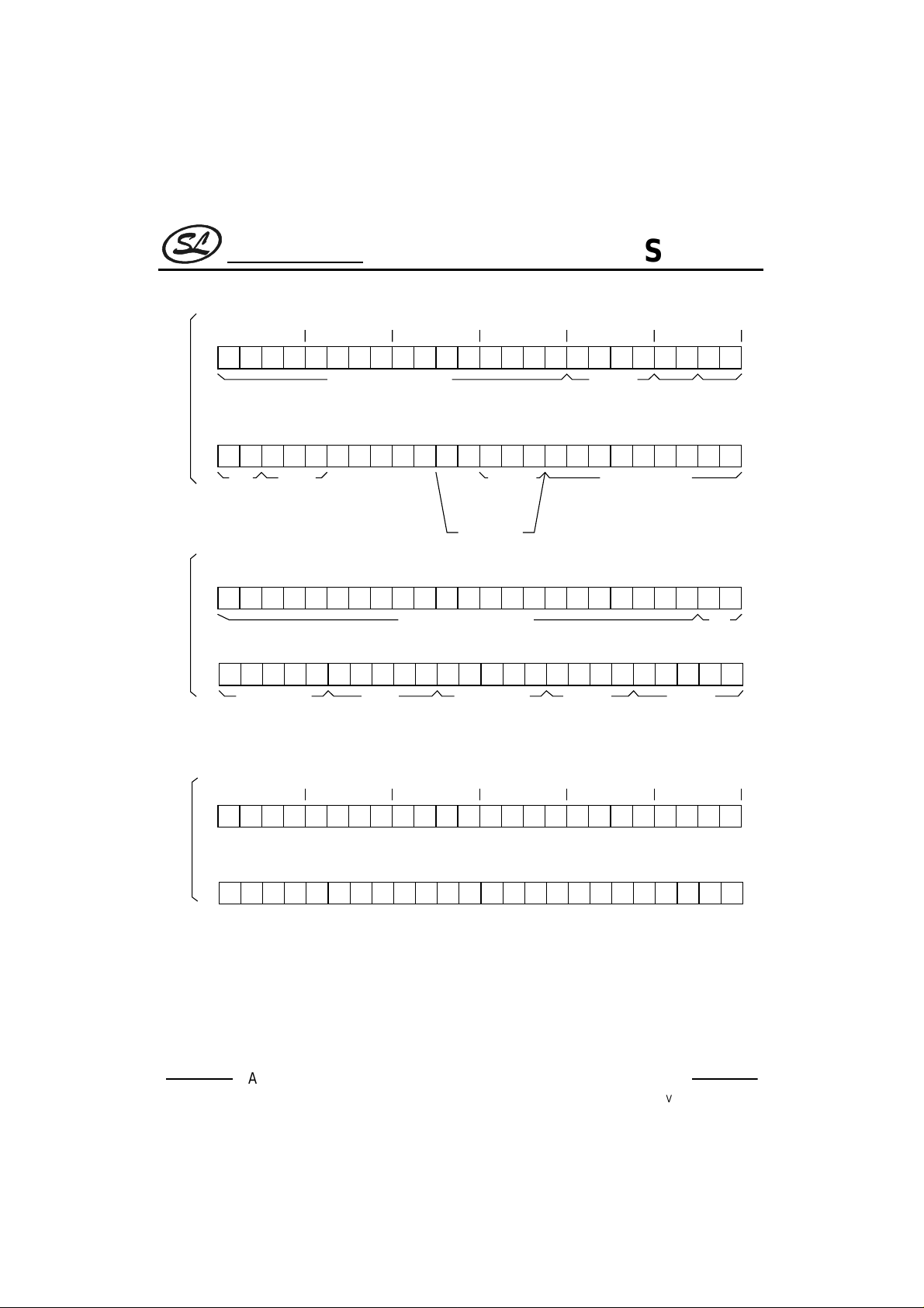
Serial transfer format
The serial transfer format consists of 8 address bits and 24 data bits (Fig. 1). Addresses D0H~D3H are used.
Start
PERIOD
CLOCK
DATA
•
Serial data transfer
serial data are transferred in sync with the clock signal. In the idle state, the PERIOD, CLOCK and DATA pin
lines are all set to “H” level. When the period signal is at “L” level, the falling of the clock signal initiates serial
data transfer. Data transfer ceases when the period signal is set to “L” level when the clock signal is at “H” level.
Once serial data transfer has begun, however, no more than 8 falls of the clock signal can occur during the time
the period signal is at “L” level.
Since the receiving side receives the serial data as valid data when the clock signal rises, it is effective for the
sending side to produce output in sync with the clock signal fall.
To receive serial data from the output registers (D1H, D3H), set the serial data output to high impedance after
the 8 bit address is output but before the next clock signal falls.
Data reception subsequently continues until the period signal becomes “L” level; data transfer ends just before
the period signal rises. Therefore, the data pin must have an open-drain or tristate interface.
Note: 1. when power is turned on, some internal circuit have undefined states. To set internal circuit states,
execute a dummy data transfer before performing regular data transfer.
2. times t1~t8 have the following value:
t1≥1.0µs
t2≥1.0µs
t3≥0.3µs
t4≥0.3µs
t5≥0.3µs
t6≥1.0µs
t7≥1.0µs
t8≥0.3µs
3. Asterisks represent numbers taken from addresses, as in D*H.
t3
t4
t1 t2
t8
(*)(*)0010 11
LSB
8addressbits
Fig.1
t5
9 clock signal fall
MSB LSB
24 data bits
(24bit register)
SC9256
End
t6
t7
MSB
HANGZHOU SILAN MICROELECTRONICS JOINT-STOCK CO.,LTD
REV: 1.0 2002.01.30.
8
 Loading...