

SILAN SC9243, SC9243S Datasheet
Silan
p
Semiconductors
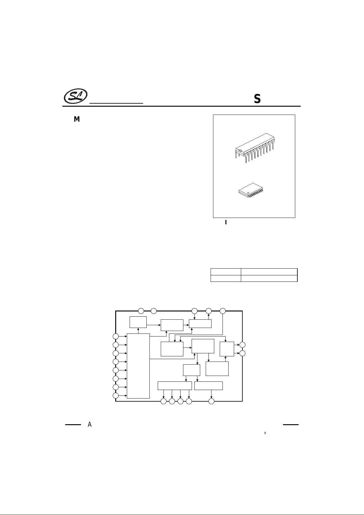
REMOTE CONTROL TRANSMITTER
DESCRIPTION
SC9243 is an infrared remote control transmitter utilizing CMOS
Technology specially designed for electrical appliances such as
Audio System, Television, Video Cassette Recorder, CD Player and
others. SC9243 is ca
144 instructions is possible. The pin assignments and application
circuit are optimized for easy PCB Layout and cost saving
advantage.
FEATURES
* CMOS Technology, Low Power Consumption
* Least External Components
* Up To 144 Instructions (32 Basic + 112 Multiple Keys)
* Multiple Keying Is Possible
* Wide Range Of Operating Supply Voltage: 2~4 Volts
* 7 Out Of 8 System Code Bits Are Pre-Settable
* Interference From Other Equipment Or Apparatus Is Prevented.
BLOCK DIAGRAM
able of multiple keying; thus, a maximum of
VSS VDD OSCI OSCO TEST
1 20 3 2 4
KI0
KI1
KI2
KI3
KI4
KI5
KI6
KI7
Reset
Circuit
5
6
7
8
9
10
11
12
Key
Input
Scan
Circuit
Oscillator
Control
Frequency
Division
Circuit
Scan
Control
Key Output Signal
Generator
13 14 15 16 17
Oscillator
Circuit
Function
Generator
Circuit
SC9243
APPLICATIONS
*MiniCOMPO
* Video Cassette Recorder(VCR)
* CD-Player
* Audio Equipment
ORDERING INFORMATION
SC9243
SC9243S
Code
Output
Code
Generator
Circuit
CODE Port
Circuit
CODEKO0 KO1 KO2 KO3
DIP-20 Package
SOP-20 Package
LED
18
19
DOUT
DIP-20
SOP-20
HANGZHOU SILAN MICROELECTRONICS JOINT-STOCK CO.,LTD
Rev: 1.1 2002.02.28
1
Silan
Semiconductors
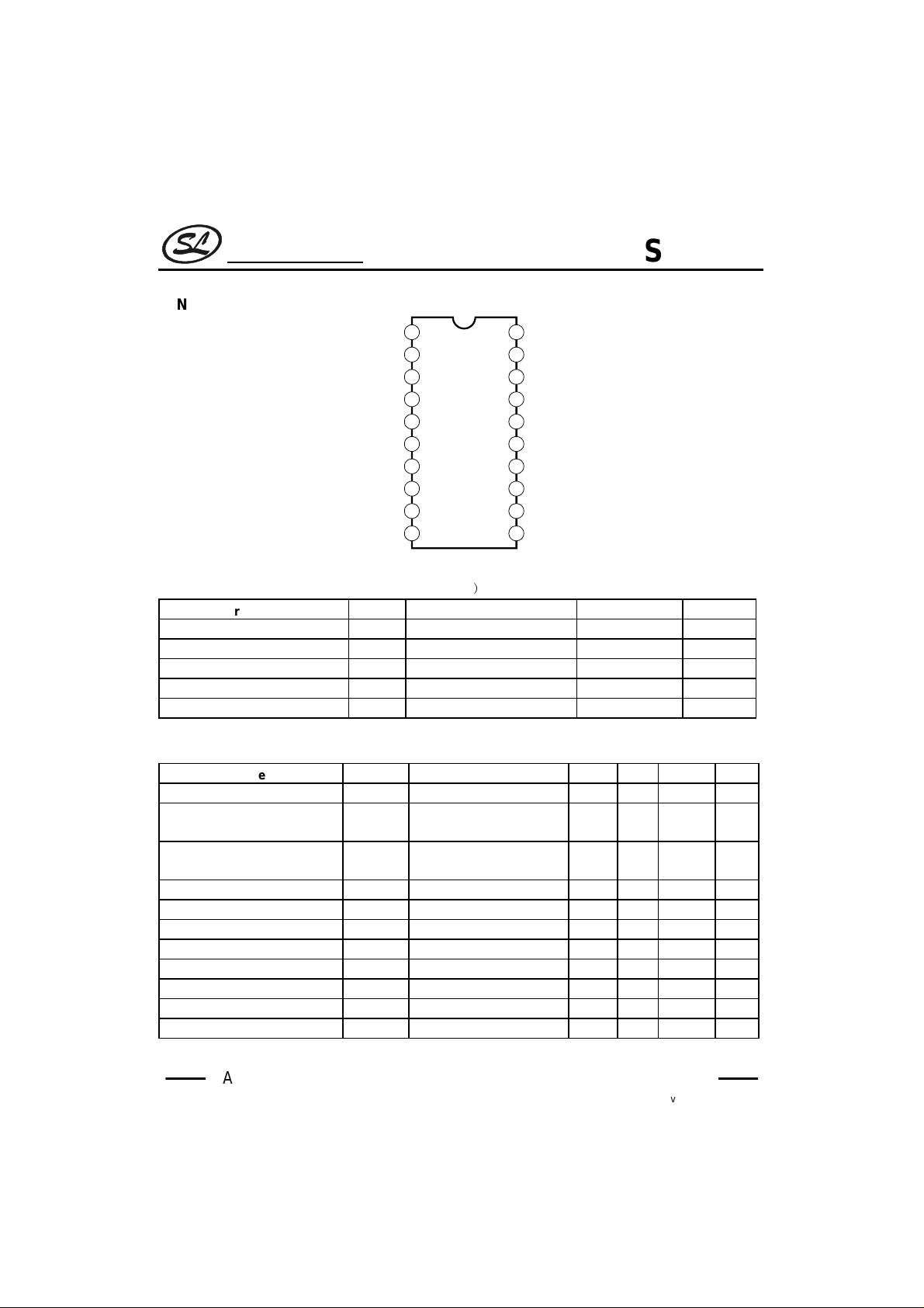
PIN CONFIGURATION
1
V
SS
2
OSCO
3
OSCI
4
TEST
5
KI0
KI1
KI2
KI3
KI4
KI5 KI6
6
7
8
9
10
SC9243
20
V
DD
19
OUT
D
18
LED
17
CODE
16
KO3
KO2
15
KO1
14
KO0
13
KI7
12
11
ABSOLUTE MAXIMUM RATING
(Tamb=>25°C
Characteristic Symbol Test conditions Value Unit
Supply Voltage V
Input Voltage With Respect To V
DD
V
ss
VDD=3 V All outputs floating Vss-0.3~VDD+0.3 V
IN
Power Dissipation Pd 300 mW
Storage Temperature Tstg -40~125
Operating Temperature T
OPR
VDD=3 V -20~70
ELECTRICAL CHARACTERISTICS
(Tamb=25°C,VDD=3V)
Parameter Symbol Test conditions Min Typ Max Unit
Operating supply Voltage V
Operating Supply Current I
Stand-By Current I
All Function Operating 2.0 3.0 4.0 V
DD
Key On Without Load
DD
=455 KHz
F
OSC
All Keys Off Stops Oscillation
SB
Output Floating.
Input Leakage Current(KI0~KI7) I
Dout Driving Current I
LED Sinking Current I
Input High Level Voltage V
Input Low Level Voltage V
VIN=GND 1.0
IL
VDD=3V VO=1.5V 10 mA
OH
VDD=3V VO=1.5V -5 mA
OL
IH
IL
Oscillation Frequency fosc 400 455 800 kHz
Pull-down Resistor Rd KI0~KI7 Pins 100 200 400
Pull-up Resistor Rup Test Pin 25 50 100
0.7 V
00.3VDDV
HANGZHOU SILAN MICROELECTRONICS JOINT-STOCK CO.,LTD
2
SC9243
-0.3 ~ 5.0 V
1000
1
DD
V
DD
Rev: 1.1 2002.02.28
°C
°C
µA
µA
µA
V
kΩ
kΩ
Silan
Semiconductors
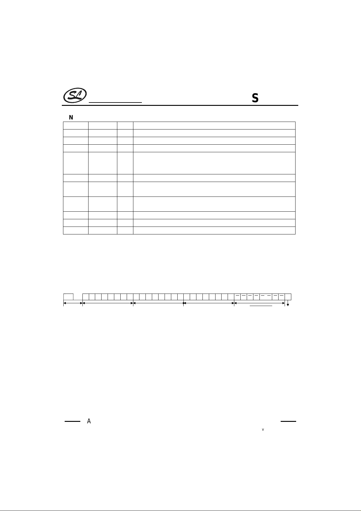
PIN DESCRIPTION
Pin No. Symbol I/O Description
1VSS-- Negative Power Supply
2 OSCO O Oscillator Output Pin with Built-in Amplifier Circuit and Feedback Resistor
3 OSCI I Oscillator Input Pin with Built-in Amplifier Circuit and Feedback Resistor
Test Pin with Built-in Pull-up Resistor. Typical value is 50k Ohms. When Test
4 TEST I
5~12 KI0~KI7 I Key Matrix Input Pins. Each pin has a built-in pull-down resistor(200k Ohms)
13~16 KO0~KO3 O
17 CODE O
18 LED O Transmission Display Output Pin
19 D
20 V
OUT
DD
Pin is connected to the VSS, Test Mode is activated. Dout Pin output
waveform shrinks 15 times without 38KHz carrier waveform
Key Scan Output Pins. Normal Operation at “L” level when there is no Key
Input.
Code Scan Output Pin. This Pin is an open drain type and used for system
code setting.
O Infrared LED Driving Output Pin
-- Positive Power Supply
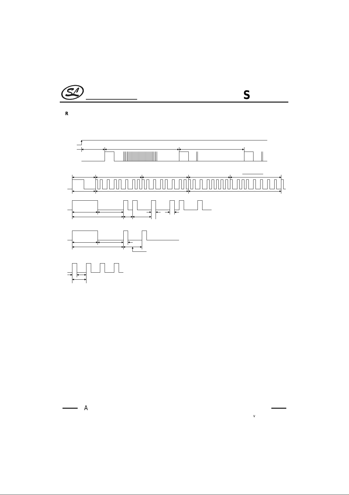
FUNCTIONAL DESCRIPTION
1. TRANSMISSION CODE
The transmission code consists of a leader code, 16 bits system code, and 8 bits data code. The inverse of the
data code is also sent simultaeously. The following diagram shows this one frame construction.
SC9243
S0 S1 S2 S4S3 S5 S6 S7 S0 S1 S2 S4S3 S5 S6 S7 D0 D2D1 D3 D4 D5 D6 D7
leader
Code
It should be noted that System Code Bit 7(S7) has a fixed value of “1”.
The leader code consists of a 4.5 ms carrier waveform followed by a 4.5 ms OFF waveform. It is used as the
leader for the following codes. Thus, when reception is configured by a microcomputer, the time relationship
between the detection of the reception and the other processes can be managed efficiently. The code uses the PPM
(Pulse Position Modulation )Method, with “0”and “1” differentiated by the time between pulses.
System Code Key Data Code
D0 D2D1 D3 D4 D5 D6 D7
Key Data CodeSystem Code
Reference
Bit
HANGZHOU SILAN MICROELECTRONICS JOINT-STOCK CO.,LTD
Rev: 1.1 2002.02.28
3
Silan
Semiconductors
2.REMOTE OUTPUT WAVEFORMS
SC9243 Remote Output Waveforms are given in the diagram below.(for fosc=455KHz)
DOUT Output Waveform
Key On
Data Transimission Waveformabort 108msabout 38ms
Data Transmission Waveform
ContinuousTransmission Waveform
about 108ms
Key Data Code
SC9243
Key Data CodeSystem CodeSystemCodeLeader Pulse
9ms 17.92ms~36ms 27ms
4.5ms 4.5ms
9ms 1.2ms 2.25ms
01 1 10
0.56ms
0.56ms
Continuous Transmission Waveform
4.5ms 4.5ms
9ms
Carrier Waveform
2/3
1/3
38KHz
0.56ms
2.25ms
in case of S0(System Code Bit0)=0
When oscillation frequency is 455 KHz, a signal is outputted after pulse is modulated by 38 KHz of duty 1/3
(which is 1/12 of the carrier generation circuit).
Note: In preparing the firmware of the receiving circuit, please strictly follow the following instructions:
1. System Codes: The same code is transmitted twice and therefore, always decode these 2 codes and check if they
are in agreement with each other.
2. Key Data Codes: The Key Data Code and its inversed code are always transmitted together, therefore, check if
they are in agreement with each other.
HANGZHOU SILAN MICROELECTRONICS JOINT-STOCK CO.,LTD
Rev: 1.1 2002.02.28
4
Silan
Semiconductors
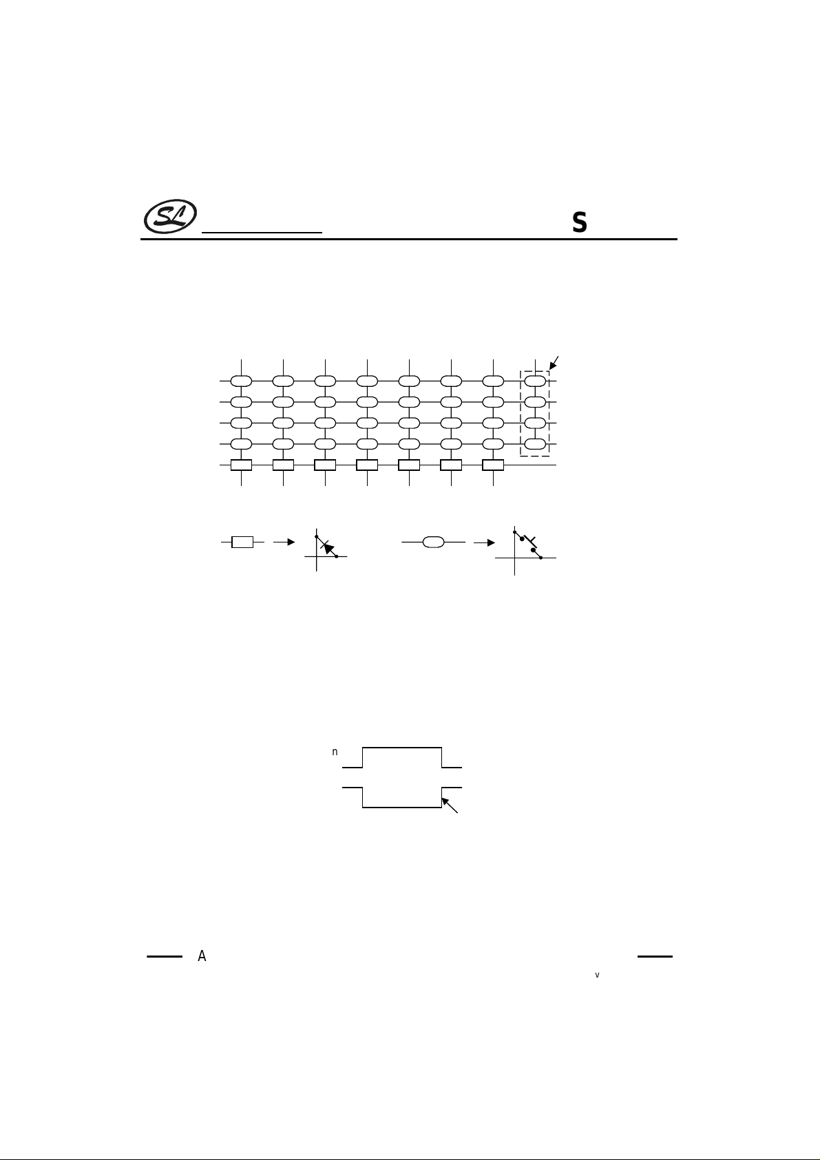
3. KEY MATRIX
SC9243 enables the maximum setting of up to 32 keys through a combination of KI0 to KI7 and KO0~KO3.
Furthermore, the System Codes are settable in 7 bits through the combination of KI0~KI6 and Code Key. Please
refer to the diagram below:
SC9243
KI0KI1 KI2KI3 KI4KI5 KI6KI7
K1 K2 K3 K4 K5 K6 K7 K8
K09 K10 K11 K12 K13 K14 K15 K16
K17 K18 K19 K20 K21 K22 K23 K24
K25 K26 K27 K28 K29 K30 K31 K32
SD0
Note:
System Code Diode Jumper
Key Nos.K8,16,24 and 32 (the Shift Keys ) can be pressed simultaneously or in any random order withother keys
(normal keys).
The system code setting is constructed by connecting the diode jumper between Code Key and KI0~KI6 keys.
With the diode jumper, the system code will have the value of “1”. If Code and any one of the KI0~KI6 keys are
connected only at one point, the diode jumper may be disregarded.
4.LED TERMINAL
When there is no key activity, the LED Pin is in the HIGH Level. Please refer to the diagram below.
SD1 SD2 SD3 SD4 SD5 SD6
Key Switch
SDn Kn
Key In
SHIFT KEYS
KO0
KO1
KO2
KO3
CODE
LED Pin
Low Activity
HANGZHOU SILAN MICROELECTRONICS JOINT-STOCK CO.,LTD
Rev: 1.1 2002.02.28
5
 Loading...