

SILAN SC431 Datasheet
Silan
Semiconductors
PFM CONTROLLED SET UP DC/DC
CONVERTERS
DESCRIPTION
The SC431XX series is a group of PFM (frequency)
controlled set-up DC/DC converters. The SC431XX Series
employs CMOS process and laser trimming technologies to
attain low power and high accuracy.
A common problem among pagers is one of noise, but with
the SC431XX, high frequency noise that occurs during switching
is reduced .
Output voltage is programmable in 0.1V steps between
2.0V-7.0V and maximum frequency is 100KHz (typ).
With a built-in switching transistor, a step-up circuit can be
configured using a coil, diode and capacitor connected
externally.
Also available is a CE (chip enable) function that reduces
power consumption during shutdown mode, and an independent
V
pin function (separated power supply and voltage detect
DD
pins) for fly-back circuit.
FEATURES
* Low noise
* Operating voltage range: 0.9V-10V
* Output voltage range: 2.0V-7.0V
* Output voltage accuracy :2.5%
* Maximum oscillator frequency: 100KHz()
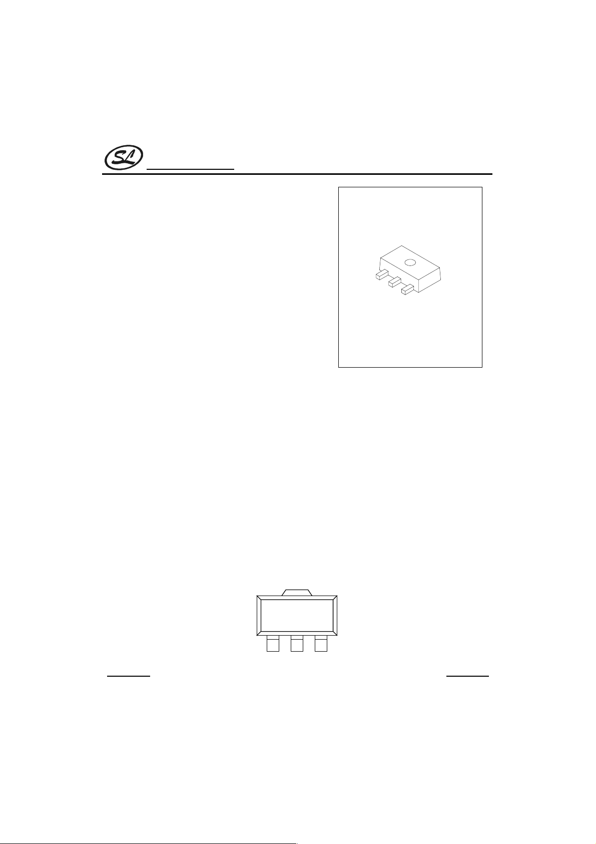
SC431XX
SOT-89
* Built-in switching transistor
* CE function and/or separated V
types
* Selectable with 5 pin packages
* Small package: SOT-89 mini-power mold (3
pin)
APPLICATIONS
* Pagers
* Palmtops
* Cameras, video cameras
* Various portable products
DD/VOUR
PIN ASSIGNMENT
HANGZHOU SILAN MICROELECTRONICS JOINT-STOCK CO.,LTD
SOT-89
123
1
Rev: 1.0 2001.02.02
Silan
Semiconductors
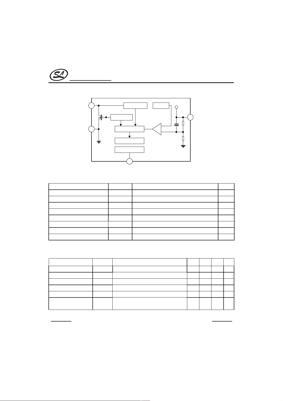
BLOCK DIAGRAM
LX
V
VLXlimiter V
Buffer
ref
DD
SC431XX
V
OUT
V
SS
PFM controll
100kHz
OSC
Chip enable
CE
ABSOLUTE MAXIMUM RATING
Characteristic Symbol Value Unit
V
pin voltage V
OUT
LX pin voltage V
LX pin current I
CE pin voltage V
VDDpin voltage V
Continuous total power dissipation P
Storage temperature T
Operating Temperature T
(Tamb=25°C)
OUT
LX
LX
CE
DD
D
STG
OPR
12 V
12 V
400 Ma
VSS-0.3~V
-30 ~ +80 °C
-40~+125 °C
+0.3 V
OUT
12 V
500 mW
ELECTRICAL CHARACTERISTICS
SC431XX-01
Parameter Symbol Test conditions Min Typ Max Unit
Output voltage V
Maximum input voltage V
Operation start-up voltage V
Operation hold voltage V
No –load input current I
Supply current 1 I
External components connected 2.94 3.00 3.06 V
OUT
IN
External component connected. I
ST
External component connected. I
HID
VIN=output voltage x 0.6, I
IN
No external components. Apply output voltage
DD1
x0.95toV
(Tamb=25°C, fosc=32768Hz,unless otherwise specified)
10 V
=1mA 0.80 0.90 V
OUT
=1mA 0.70 V
OUT
=0mA (note1). 4.6 9.3 µA
OUT
OUT.
19.7 39.4 µA
(To be continued)
HANGZHOU SILAN MICROELECTRONICS JOINT-STOCK CO.,LTD
2
Rev: 1.0 2001.02.02
Silan
Semiconductors
(Continued)
Parameter Symbol Test conditions Min Typ Max Unit
Supply current 2 I
Lx switch-on resistance R
Lx leakage current I
No external components. Apply output voltage
DD2
x0.95toV
No external components. Apply output voltage
SWON
x0.95toV
No external components. V
LXL
OUT.
OUTVLX
=0.4V.
=10V 1.0
OUT=VLX
No external components. Apply output voltage
Duty ratio DTY
x0.95toV
LX: 300Ω pull-up to 5V.
OUT
Measuring of LX waveform.
Maximum oscillation
frequency
MAX F
No external components. Apply output voltage
OSC
x0.95toV
LX: 300Ω pull-up to 5V. Duty
OUT
ratio 75%. Measuring of LX waveform.
No external components. Apply output voltage
Lx limit voltage V
LXLMT
x0.95toV
. Apply voltage to LX. Voltage
OUT
required to produce FOSC x 2.
Efficiency (note3) E
External component connected. 80 %
FFI
SC431XX-02
Parameter Symbol Test conditions Min Typ Max Unit
Output voltage V
Maximum input voltage V
Operation start-up voltage V
Operation hold voltage V
No –load input current I
Supply current 1 I
Supply current 2 I
Lx switch-on resistance R
DD1
DD2
SWON
External component connected. 2.94 3.00 3.06 V
OUT
IN
External component connected.
ST
I
=1Ma.
OUT
External component connected.
HID
I
=1mA.
OUT
VIN=output voltage x 0.6,
IN
I
=0mA (note1)
OUT
No external components.
Apply output voltage x 0.95 to V
OUT.
No external components.
Apply output voltage x 0.95 to V
OUT.
No external components.
Apply output voltage x 0.95 to V
OUT
VLX=0.4V.
SC431XX
2.1 4.2
5.2 7.9
70 75 80 %
85 100 115 KHz
0.7 1.1 V
10 V
0.80 0.90 V
0.70 V
4.6 9.3
19.7 39.4
2.1 4.2
5.2 7.9
(To be continued)
µA
Ω
µA
µA
µA
µA
Ω
HANGZHOU SILAN MICROELECTRONICS JOINT-STOCK CO.,LTD
3
Rev: 1.0 2001.02.02
 Loading...