

Page 1
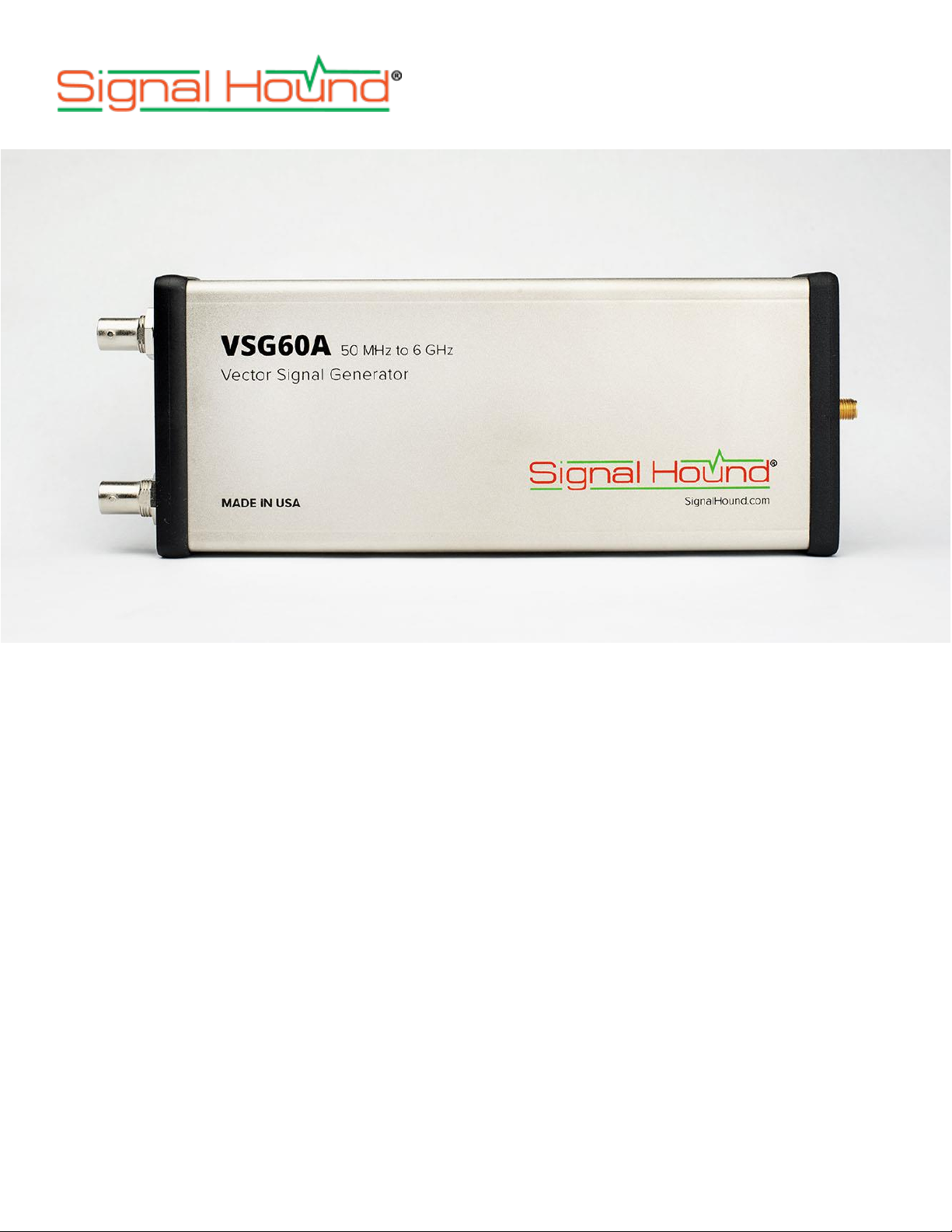
VSG60A Vector Signal Generator
Product Manual
Page 2

ii
Signal Hound VSG60A Product Manual
Published 8/23/2019
© 2019, Signal Hound, Inc.
1502 SE Commerce Ave, Suite 101
Battle Ground, WA USA
Phone 360.313.7997
This information is being released into the public domain in accordance with the Export Administration
Regulations 15 CFR 734
Page 3
iii
Contents
1 Introduction .......................................................................................................................................................... 1
2 Understanding the Hardware ............................................................................................................................. 2
3 Capabilities ........................................................................................................................................................... 6
4 Calibration ............................................................................................................................................................ 6
5 Adjustments ......................................................................................................................................................... 6
6 VSG60A Preliminary Specifications .................................................................................................................. 7
7 Typical Performance ......................................................................................................................................... 10
Page 4

Introduction | Preparing for first use
1
1 Introduction
The Signal Hound VSG60A Vector Signal Generator offers mid-range performance and agility at an
affordable price. Continuously streaming up to 40 MHz of bandwidth at up to 51.2 MSPS from a PC
or laptop virtually eliminates I/Q pattern buffer size restrictions.
The VSG60A hardware features an agile low phase noise LO synthesizer, digital baseband
oversampling with reconstruction filter, harmonic filters across the full frequency range, and a trigger
output, timed to match the RF output, for integrating the VSG60A in to test systems.
I/Q phase, amplitude, and offset are corrected across RF frequency, baseband frequency, and
temperature in our environmental chamber, and stored on the VSG60A. The software applies these
corrections in real-time.
Commands to change frequency and amplitude are embedded in the same data stream from the PC
as the I/Q data, giving the user precise timing across frequency and amplitude changes. The agile
LO can change frequency and settle in 200 µs and offers outstanding phase noise.
PREPARING FOR FIRST USE
• Install the VSG60A software, either from signalhound.com or the included CD.
• Plug in the VSG60A using the included USB Y cable by first connecting the USB 3.0 type A
connector to a USB superspeed port on your PC or laptop. Then plug in the thinner USB 2
type A connector (for extra power). Finally, plug in the micro-B connector to the VSG60A until
it is fully seated and tighten the thumb screws. Do not overtighten. You should see a solid
green LED on the VSG60A.
o Note: The VSG60A is intended for use only with the included USB cable. Longer
cables may result in an intermittent connection, especially around electromagnetic
interference.
• Launch the software.
Page 5
Understanding the Hardware | Preparing for first use
2
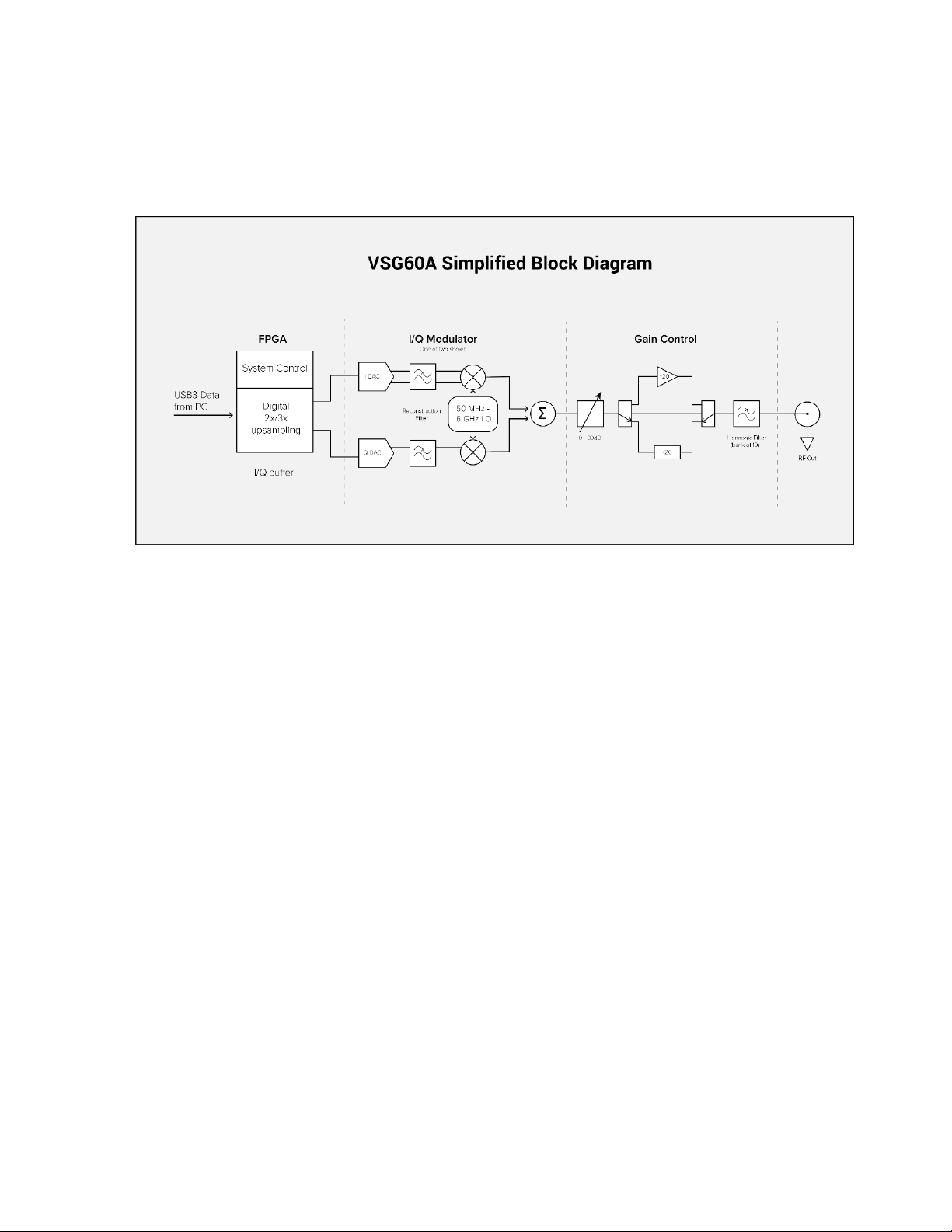
2 Understanding the Hardware
At the heart of the VSG60A is pair of quadrature modulators, one for below 2 GHz, and one for above
2 GHz (and a small segment around 800 MHz), driven by a dual channel DAC. The DAC clocks in
I/Q samples at 66-102 .4 MSPS. The data rate from the PC to the FPGA is 22-51.2 MSPS I/Q, so
inside the FPGA we digitally up-sample by a factor of 2 or 3. This allows the use of a single optimized
reconstruction filter for typically better than 60 dB rejection of any aliased baseband signals, and
allows the PC to efficiently up-sample the user-selected baseband clock rate by a simple power of
two.
The baseband clock is generated from a 2.4 to 2.8 GHz VCO and divided down to 66-102.4 MHz.
Standard telecom symbol rates can be produced with 0 ppm additive error, and any symbol rate can
be produced with less than 1 ppm error.
The local oscillator (LO) generates a low phase noise CW signal (typically -125 dBc/Hz at a 10 kHz
offset from 1 GHz) for the I/Q modulators. Below 2 GHz, the LO runs at twice the RF frequency and
is digitally divided into quadrature. Above 2 GHz, a polyphase filter generates the quadrature LO for
the mixers. The LO switches frequencies in 200 microseconds for frequency-hopping applications.
The LO has 1/6 Hz resolution when digital tuning is disabled, and better than 1 µHz when digital tuning
is enabled. See the section on digital tuning for more information.
Both the baseband clock and LO are synthesized from a low phase noise 80 MHz clock, tied to either
the internal 10 MHz voltage-controlled, temperature-compensated crystal oscillator (VCTCXO), or the
user’s external 10 MHz input.
From the modulators, up to 20 dB of gain or 50 dB of attenuation is applied, in 2 dB steps. The
VSG60A software typically automatically selects the best setting based on output amplitude, but
Page 6
Understanding the Hardware | External 10 MHz input
3
manual control is available as well. Fine amplitude control is handled digitally, providing 0.01 dB
resolution on the output amplitude.
Finally, a bank of harmonic filters reduces the amplitude of harmonics generated from the modulators
and amplifiers, typically below -40 dBc.
The FPGA in the VSG60A can quickly switch between streaming I/Q and changing LO frequency or
attenuator settings at precise intervals (200 µs and 10 µs, respectively), allowing the user to build
signals that hop across the entire frequency range of the device. This makes the VSG60A a good
choice for generating frequency hopping signals or signals that must cover a wide amplitude range.
EXTERNAL 10 MHZ INPUT
A low-jitter comparator provides low additive phase noise for an external 10 MHz reference input of 0
dBm to +13 dBm. When external reference is enabled, the internal 10 MHz VCTCXO is disabled and
the external reference disciplines the 80 MHz VCXO directly. Inputs as low as -15 dBm will work, but
phase noise degrades at lower amplitudes. A square wave provides the highest slew rate and
therefore the best phase noise.
TRIGGER OUTPUT
The trigger output is a series-terminated 3.3V logic signal, meant to typically drive a high impedance
load. The trigger output is synchronized with the RF output. Up to 1000 triggers per second can be
output, with a user-selectable pulse width. This enables the VSG60A to be connected to other
equipment in an automated testing environment.
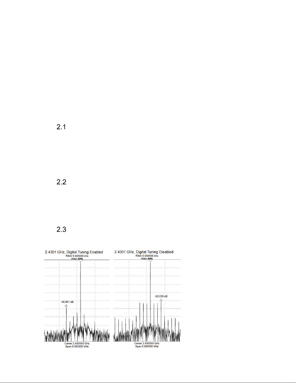
LOW SPUR MODE (DIGITAL TUNING)
The LO uses a fractional-N PLL. This can lead to integer boundary spurs, as well as other spurious.
To mitigate these spurs, a low spur
mode has been added, which is on
by default. When low spur mode is
enabled, the fractional-N PLL uses a
very low denominator to keep the
spurs at least 2 MHz away from the
carrier and typically below -50 dBc
above 3.7 GHz, and below -55 dBc
below 3.7 GHz. This gives a coarse
LO frequency, which is then digitally
tuned to the exact requested
frequency. The advantages of digital
tuning are very low-level, predictable
Page 7

Understanding the Hardware | Linearity and compression
4
fractional-N and integer boundary spurs, and nearly infinite tuning resolution. The disadvantage is that
the hardware’s I/Q offset is no longer centered in the modulation envelope.
For applications where digital tuning is not desirable, such as protocols that require the hardware I/Q
offset to be centered, digital tuning should be disabled. This sets the fractional-N PLL for 1/6 Hz
resolution, allowing 1 Hz steps and frequencies like 833 1/3 MHz with zero additive frequency error.
Most frequencies in this mode will have fractional-N spurs below -50 dBc, but some frequencies will
have close-in spurs that exceed this level.
LINEARITY AND COMPRESSION
To keep the VSG60A USB-powered, it was designed with modulators and amplifiers that strike a
balance between linearity and power consumption. The best linearity is obtained at output levels of
-10 dBm or lower, where 3rd order intermodulation products are typically below -50 dBc, and generally
linearity is better at lower frequencies. For frequencies above 3 GHz at amplitudes above 0 dBm,
compression and intermodulation distortion may become an issue for some signals. Above 4 GHz, a
+10 dBm CW output may be compressed by about 1 dB in places, and compression at this level will
significantly impair EVM. Applications requiring good linearity at high output power, especially at high
frequencies, may require an external amplifier. An amplifier with a third order intercept 25 dB above
the required output power will generally preserve the linearity of the VSG60A.
IMPROVING VSWR, IF FLATNESS, MISMATCH UNCERTAINTY
The VSG60A harmonic filters have fairly high VSWR at certain frequencies. When connecting to a
high VSWR receiver or antenna, a 3 to 10 dB fixed SMA attenuator connected to the VSG60A output
significantly reduces mismatch uncertainty and VSWR, and improves the IF flatness for applications
where this is a concern.
AMPLITUDE CONTROL AND SWITCHING
Internally, the VSG60A has 3 coarse gain settings, usually controlled by the API. High gain uses an
amplifier with a 20 dB gain. Mid-gain is 0 dB (bypass both amplifier and attenuator). Low gain is a 20
dB attenuator. The amplifier is powered on for both high gain and mid gain, but powered off for low
gain. Additionally, there is a 0-30 dB step attenuator, calibrated in 2 dB steps. Fine amplitude control
is accomplished digitally by scaling the I/Q data. The final amplitude state is “off”, which powers down
the I/Q modulators and amplifiers.
The VSG60A can switch amplitudes in 10 microseconds. This is a fixed delay to allow for switches,
atenuators, and amplifiers to settle a bit. However, when switching directly from low gain amplitudes
(such as -40 dBm) to high gain amplitudes (such as +5 dBm), the output amplifier must turn on and
Page 8

Understanding the Hardware | Hardware-Software interface
5
stabilize. The output power will be within 1 dB (0.6 dB typical) of its final power within 10 microseconds,
but typically requires 5 milliseconds to stabilize to within 0.1 dB.
Please note that for ramping amplitude from low to high, 2 dB steps every millisecond for example,
the amplifier is powered on but not used for a 20 dB range, giving plenty of time for the amplifier to
fully stabilize before it is used. Also, if the amplitude is fully controlled with the I/Q data, this problem
is avoided altogether.
HARDWARE-SOFTWARE INTERFACE
Other than up-sampling by 2 or 3 on the FPGA, all digital signal processing happens on the PC. The
VSG60A software and API automatically adjust the signal amplitude, I/Q balance and DC offset to
provide an accurate, clean, flat 40 MHz modulation bandwidth. A highly optimized FIR filter on the PC
applies these corrections in real-time with minimal software overhead.
An array of correction constants across frequency and temperature is generated by running each
VSG60A through an environmental chamber and storing this data to internal flash memory.
A state machine inside the FPGA processes I/Q data, triggers, frequency steps, and amplitude steps.
This allows precise timing relationships between events such as frequency hops.
OPTIMIZING PERFORMANCE
Pulse Modulation
When using our user interface software, the “off” state can be optimized by changing the I/Q offset to
minimize the LO feed-through until a spectrum analyzer, such as the SM200A, reads a minimum
amplitude. Typically, 60 dB on/off ratio is possible using this method.
When using the API, two additional tricks are available. If the pulse will be sent to a receiver with 20
MHz bandwidth or less, converting the pulse to a 15-16 MHz offset tone will place the LO feed-through
in the “off” state outside the 20 MHz bandwidth.
Spurious
The VSG60A uses a fractional-N synthesizer. If your application allows for some flexibility in frequency
selection, sticking to even multiples of 4, 5, or 10 MHz for your center frequency will reduce or
eliminate fractional-N spurs.
Bandwidth
For a 50 MSPS sample rate, digital filters in the FPGA begin to roll off just past an 18 MHz offset, and
are down about 1 dB by 20 MHz offset from center. By keeping signal bandwidth to 72% or less of
Page 9

Capabilities | Timebase
6
the I/Q sample rate, the VSG60A will maintain excellent flatness across the signal’s bandwidth.
Please note that for sample rates below 25 MSPS, the API will up-sample the I/Q data, and there is
no penalty for using a bandwidth up to 80% of the sample rate.
When using the API, the user is expected to keep the signal bandwidth confined to 80% of the sample
rate. Violating this will result in spurious responses.
3 Capabilities
As a vector signal generator, the VSG60A can generate virtually any signal that fits within its 40 MHz
bandwidth, limited only by the waveform generation software. The VSG60A ships with a powerful
suite of software tools for generating both analog and digital modulation, adding impairments for
receiver testing, or loading custom waveforms, all at no additional cost. A user-friendly application
programming interface (API) is available for communicating with the VSG60A directly from your
software application. See the VSG60A software and API manuals for more information.
4 Calibration
Our Field Calibration Software is available as a free download and may be used to calibrate the
VSG60A. Check the Field Calibration software manual for required equipment.
5 Adjustments
Adjustments to the VSG60A are done in an environmental chamber at the Signal Hound production
facility. Here, the timebase is initially adjusted, and the I/Q balance, DC offset, and output amplitude
are adjusted across frequency and temperature. Additionally, the user can adjust the internal
timebase as needed, and manually adjust the DC offset to null out the LO feedthrough, if the factory
adjustment is insufficient for a particular task, such as improving the on/off ratio for pulse modulation.
TIMEBASE
The 10 MHz internal timebase is a voltage-controlled, temperature-compensated crystal oscillator
(VCTCXO) with a 16-bit DAC, providing sub-part per billion resolution. It is factory adjusted before
shipping and may be software-adjusted in the field as needed. For a VSG60A operating at a stable
temperature, periodic adjustments will typically keep the internal timebase to better than 0.1 ppm.
Page 10

VSG60A Preliminary Specifications | Timebase
7
6 VSG60A Preliminary Specifications
Unless otherwise noted, the specifications listed are under default conditions, digital tuning enabled.
Frequency
Specified Range
All Modes
50 MHz to 6 GHz
Useable Range (typical)
All Modes
30 MHz to 6 GHz
Resolution
Digital Tuning Disabled
1/6 Hz
Digital Tuning Enabled
< 1 µHz
LO Switch Time
Queued Hops
200 µs
Software-controlled
80 ms typical
Accuracy
Internal timebase, Aging
+/- 1 ppm/yr
Initial accuracy
+/- 1 ppm
I/Q Symbol Clock Range
All Modes
12.5 kHz to 51.2 MHz
I/Q Symbol Clock Accuracy
All Modes
+/- 1 ppm + timebase
accuracy
Commonly used symbol rates
0 ppm + timebase accuracy
I/Q Symbol Clock Switch Time
All modes
100 ms typical
Page 11

VSG60A Preliminary Specifications | Timebase
8
Level
Specified Range
CW Mode
-55 dBm to +7dBm
Useable range
All modes
-80 dBm to (+10 dBm –
PAPR)1
Absolute level error
CW mode, -55 to +7 dBm
+/- 2.0 dB
Modulation Flatness
20 MHz BW, 1 GHz carrier
+/- 0.5 dB
40 MHz BW, 1 GHz carrier
+/- 2.0 dB
Switching Time
All modes
10 µs
Settling Time
< 20 dB step
<10 µs typical to 0.1 dB
> 20 dB step
<10 µs typical to 1 dB
5 ms typical to 0.1 dB
Reverse Power
Damage Level
+20 dBm
1
PAPR = Peak-to-Average Power Ratio
Page 12

VSG60A Preliminary Specifications | Inputs / Outputs
9
Spectral Purity
Harmonics
50 MHz to 6 GHz, CW, 0 dBm
< -30 dBc
Image Response
50 MHz to 6 GHz, -10 dBm,
20 MHz modulation bandwidth
< -40 dBc
50 MHz to 6 GHz, -10 dBm,
40 MHz modulation bandwidth
< -30 dBc
Carrier Feedthrough
50 MHz to 6 GHz, CW, 0 dBm
< -40 dBc
SSB Phase Noise
1 GHz CW, 0 dBm
10 kHz offset
100 kHz offset
< -120 dBc/Hz
< -122 dBc/Hz
Other non-harmonic Spurious
Carrier 50 MHz to 6 GHz
Digital tuning enabled
Modulated with 1 MHz tone
Level -10 dBm,
Spurs measured to 1.7x center
frequency
< -40 dBc
Error Vector Magnitude (EVM)
(-10 dBm output power)
QPSK, 4 MS/s, 0.2RRC
< 3 GHz
3-6 GHz
QAM16, 4 MS/s, 0.2 RRC
< 3 GHz
3-6 GHz
1 GHz QAM16, 1 MS/s, 0.35 RC
< 1.2% (typ. 0.6%)
< 1.8%
< 1.0% (typ. 0.5%)
< 1.7%
< 0.5% (typ. 0.3%)
Adjacent Channel Power Ratio
(RRC 0.2, -10 dBm)
QPSK 4 MS/s, 5 MHz channel
< 3 GHz
3-6 GHz
< -50 dBc (typ. -55 dBc)
< -40 dBc (typ. -45 dBc)
INPUTS / OUTPUTS
Data and Power (1) USB 3.0 port and (1) adjacent USB 2.0 or USB 3.0 port
RF output SMA (F)
External 10 MHz Input BNC (F), 0 to +13 dBm recommended
Trigger Output BNC (F), 3.3V logic level
Page 13

Typical Performance | Mechanical / Environmental
10
MECHANICAL / ENVIRONMENTAL
Power Requirements USB-powered, 4.5 – 5.25V, 6 watts typical.
Operating temperature 0 to 50 oC
Size 8.63” x 3.19” x 1.19”
Weight about 1 lb
7 Typical Performance
VSWR (typical, at tuned frequency)
50 MHz – 1.6 GHz
< 1.62
1.6 GHz – 2.5 GHz
< 2.75
> 2.5 GHz
< 4.2
EVM
2.4 GHz, 1 MS/s QPSK, Raised cosine, alpha 0.35, -10 dBm: 0.24%; 0 dBm: 0.4%; +10 dBm: 1.1%
Page 14

Typical Performance | Typical SSB Phase Noise
11
TYPICAL SSB PHASE NOISE
Page 15

Typical Performance | Typical Amplitude Accuracy
12
TYPICAL AMPLITUDE ACCURACY
TYPICAL CARRIER FEEDTHROUGH
-0.8
-0.6
-0.4
-0.2
0
0 1000 2000 3000 4000 5000 6000
Amplitude Error (dB)
Frequency (MHz)
Typical Amplitude Accuracy vs. Frequency, -20 dBm CW
-100
-90
-80
-70
-60
-50
-40
0 1000 2000 3000 4000 5000 6000
Frequency (MHz)
Carrier Feedthrough (dBc)
Page 16

Typical Performance | Typical Harmonics
13
TYPICAL HARMONICS
TYPICAL FLATNESS ACROSS 40 MHZ CHANNEL
-100
-90
-80
-70
-60
-50
-40
-30
-20
0 1000 2000 3000 4000 5000 6000
Frequency (MHz)
Typical Harmonics (dBc), 0 dBm output power
2nd Harmonic 3rd Harmonic Worst Harmonic
-1.2
-1
-0.8
-0.6
-0.4
-0.2
0
0.2
-25 -20 -15 -10 -5 0 5 10 15 20 25
dB down from Channel Center
Offset from center (MHz)
Typical Flatness Across 40 MHz Modulation Bandwidth, 1 GHz carrier
Page 17

Typical Performance | Typical other non-harmonic spurious
14
TYPICAL OTHER NON-HARMONIC SPURIOUS
-75
-70
-65
-60
-55
-50
-45
-40
0 1000 2000 3000 4000 5000 6000
dBc
Other Non-Harmonic Spurious (1 MHz Offset Tone)
 Loading...