

Page 1
© 2019 SignalCore, Inc. All Rights Reserved
Hardware Manual
SC5507A & SC5508A PSG
DC – 6.25 GHz RF Signal Source
With Sensor
www.signalcore.com
Page 2
©2019 Rev 1.0
1
General Information
Table of Contents
1 General Information ................................................................................................................................ 4
Warranty .......................................................................................................................................... 4
Copyright & Trademarks .................................................................................................................. 4
International Materials Declarations ............................................................................................... 5
CE European Union EMC & Safety Compliance Declaration ........................................................... 5
Warnings Regarding Use of SignalCore Products ............................................................................ 5
2 Physical Description ................................................................................................................................. 6
Unpacking ........................................................................................................................................ 6
Nomenclature .................................................................................................................................. 6
Setting Up and Configuring the PSG Device .................................................................................... 7
Front Interface Indicators and Connectors ..................................................................................... 7
Signal Connections ................................................................................................................... 7
Device LED Indicators .............................................................................................................. 8
Communication and Supply Connection ................................................................................. 8
Mini-USB Connection............................................................................................................... 9
Reset Button (Pin Hole) ......................................................................................................... 10
3 Theory and Operation ............................................................................................................................ 10
RF Generation ................................................................................................................................ 11
Amplitude Control ......................................................................................................................... 11
Computational Time ...................................................................................................................... 11
RF Power Sensor ............................................................................................................................ 11
Internal EEPROM............................................................................................................................ 12
Modes of RF Generation ................................................................................................................ 12
Sweep Function ..................................................................................................................... 12
List Function ........................................................................................................................... 12
Sweep Direction ..................................................................................................................... 12
Sweep Waveform .................................................................................................................. 12
Dwell Time ............................................................................................................................. 13
List Cycles ............................................................................................................................... 13
Trigger Sources ...................................................................................................................... 13
Hardware Trigger Modes ....................................................................................................... 13
Trigger Out Modes ................................................................................................................. 13
Page 3
Rev 1.0 | SC5507A & SC5508A Hardware Manual SignalCore, Inc.
2
SC5507A & SC5508A Hardware Manual
Default Startup Mode .................................................................................................................... 14
4 Hardware Registers ................................................................................................................................ 14
Configuration Registers ................................................................................................................. 14
Register 0x01 INITIALIZE (1 Byte) .......................................................................................... 16
Register 0x02 SET_SYS_ACTIVE (1 Byte)................................................................................ 16
Register 0x03 SYNTH_MODE (1 Byte) ................................................................................... 16
Register 0x04 RF_MODE (1 Byte) .......................................................................................... 17
Register 0x05 LIST_MODE_CONFIG (1 Byte) ......................................................................... 18
Register 0x06 LIST_START_FREQ (7 Bytes) ............................................................................ 19
Register 0x07 LIST_STOP_FREQ (7 Bytes) ............................................................................. 20
Register 0x08 LIST_STEP_FREQ (7 Bytes) .............................................................................. 20
Register 0x09 LIST_DWELL_TIME (7 Bytes) ........................................................................... 20
Register 0x0A LIST_CYCLE_COUNT (7 Bytes) ........................................................................ 20
Register 0x0B Reserved ......................................................................................................... 21
Register 0x0C LIST_BUFFER_POINTS (3 Bytes) ...................................................................... 21
Register 0x0D LIST_BUFFER_WRITE (7 Bytes) ....................................................................... 21
Register 0x0E LIST_BUF_MEM_TRNSFER (1 Byte) ................................................................ 22
Register 0x0F LIST_SOFT_TRIGGER (1 Byte).......................................................................... 22
Register 0x10 RF_FREQUENCY (7 Bytes) ............................................................................... 22
Register 0x11 RF_LEVEL (3 Bytes) ......................................................................................... 22
Register 0x12 RF_ENABLE (1 Byte) ........................................................................................ 23
Register 0x13 RF_PHASE (7 Bytes) ........................................................................................ 23
Register 0x14 AUTO_LEVEL_DISABLE (1 Byte) ...................................................................... 23
Register 0x15 RF_ALC_MODE (1 Byte) .................................................................................. 23
Register 0x16 RF_STANDBY (1 Byte) ..................................................................................... 24
Register 0x17 REFERENCE_MODE (1 Byte) ........................................................................... 24
Register 0x18 REFERENCE_DAC_VALUE (3 Bytes) ................................................................ 24
Register 0x1A DIRECT_ATTEN ............................................................................................... 24
Register 0x1B STORE_DEFAULT_STATE (1 Byte) ................................................................... 25
Register 0x1C SELF_SYNTH_CAL (1 Byte) .............................................................................. 25
Register 0x1D SENSOR_SETTING (3 Byte) ............................................................................. 25
Register 0x1E SENSOR_FREQUENCY (7 Byte) ........................................................................ 26
Query Registers .............................................................................................................................. 26
Page 4
©2019 Rev 1.0
3
General Information
Register 0x20 GET_RF_PARAMETERS (1 Byte sent, 8 Bytes received) ................................. 27
Register 0x21 GET_TEMPERATURE (1 Byte, 8 Bytes) ............................................................ 27
Register 0x22 GET_DEVICE_STATUS (1 Byte, 8 Bytes) .......................................................... 28
Register 0x23 GET_DEVICE_INFO (1 Byte, 8 Bytes) .............................................................. 30
Register 0x24 GET_LIST_BUFFER (3 Bytes, 8 Bytes).............................................................. 31
Register 0x25 FETCH_DAC_VALUE (1 Byte, 8 Bytes) ............................................................ 31
Register 0x26 SERIAL_OUT_BUFFER ..................................................................................... 31
5 Communication Interfaces .................................................................................................................... 33
Communication Data Format ........................................................................................................ 33
USB Interface ................................................................................................................................. 33
Control Transfer ..................................................................................................................... 33
Bulk Transfer .......................................................................................................................... 33
SPI Interface ................................................................................................................................... 34
Writing the SPI Bus ................................................................................................................ 35
Reading the SPI Bus ............................................................................................................... 35
RS232 Interface .............................................................................................................................. 36
Writing to the Device Via RS232............................................................................................ 36
Reading from the Device Via RS232 ...................................................................................... 37
PXI .................................................................................................................................................. 37
Setting Up the PCI to Serial Bridge ........................................................................................ 37
Writing to the Device ............................................................................................................. 38
Reading from the Device ....................................................................................................... 38
Revision Table ................................................................................................................................................ 39
Page 5

Rev 1.0 | SC5507A & SC5508A Hardware Manual SignalCore, Inc.
4
SC5507A & SC5508A Hardware Manual
1 General Information
Warranty
This product is warranted against defects in materials and workmanship for a period of one year from
the date of shipment. SignalCore will, at its option, repair or replace equipment that proves to be
defective during the warranty period. This warranty includes parts and labor.
Before any equipment will be accepted for warranty repair or replacement, a Return Material
Authorization (RMA) number must be obtained from a SignalCore customer service representative and
clearly marked on the outside of the return package. SignalCore will pay all shipping costs relating to
warranty repair or replacement.
SignalCore strives to make the information in this document as accurate as possible. The document has
been carefully reviewed for technical and typographic accuracy. If technical or typographical errors
exist, SignalCore reserves the right to make changes to subsequent editions of this document without
prior notice to possessors of this edition. Please contact SignalCore if errors are suspected. In no event
shall SignalCore be liable for any damages arising out of or related to this document or the information
contained in it.
EXCEPT AS SPECIFIED HEREIN, SIGNALCORE, INCORPORATED MAKES NO WARRANTIES, EXPRESS OR
IMPLIED, AND SPECIFICALLY DISCLAIMS ANY WARRANTY OF MERCHANTABILITY OR FITNESS FOR A
PARTICULAR PURPOSE. CUSTOMER’S RIGHT TO RECOVER DAMAGES CAUSED BY FAULT OR NEGLIGENCE
ON THE PART OF SIGNALCORE, INCORPORATED SHALL BE LIMITED TO THE AMOUNT THERETOFORE
PAID BY THE CUSTOMER. SIGNALCORE, INCORPORATED WILL NOT BE LIABLE FOR DAMAGES RESULTING
FROM LOSS OF DATA, PROFITS, USE OF PRODUCTS, OR INCIDENTAL OR CONSEQUENTIAL DAMAGES,
EVEN IF ADVISED OF THE POSSIBILITY THEREOF. This limitation of the liability of SignalCore, Incorporated
will apply regardless of the form of action, whether in contract or tort, including negligence. Any action
against SignalCore, Incorporated must be brought within one year after the cause of action accrues.
SignalCore, Incorporated shall not be liable for any delay in performance due to causes beyond its
reasonable control. The warranty provided herein does not cover damages, defects, malfunctions, or
service failures caused by owner’s failure to follow SignalCore, Incorporated’s installation, operation, or
maintenance instructions; owner’s modification of the product; owner’s abuse, misuse, or negligent
acts; and power failure or surges, fire, flood, accident, actions of third parties, or other events outside
reasonable control.
Copyright & Trademarks
Under the copyright laws, this publication may not be reproduced or transmitted in any form, electronic
or mechanical, including photocopying, recording, storing in an information retrieval system, or
translating, in whole or in part, without the prior written consent of SignalCore, Incorporated.
SignalCore, Incorporated respects the intellectual property rights of others, and we ask those who use
our products to do the same. Copyright and other intellectual property laws protect our products. Use
of SignalCore products is restricted to applications that do not infringe on the intellectual property rights
of others.
Page 6

©2019 Rev 1.0
5
General Information
“SignalCore”, “signalcore.com”, and the phrase “preserving signal integrity” are registered trademarks
of SignalCore, Incorporated. Other product and company names mentioned herein are trademarks or
trade names of their respective companies.
International Materials Declarations
SignalCore, Incorporated uses a fully RoHS compliant manufacturing process for our products.
Therefore, SignalCore hereby declares that its products do not contain restricted materials as defined
by European Union directive 2002/95/EC (EU RoHS) in any amounts higher than limits stated in the
directive. This statement assumes reliable information and data provided by our component suppliers
and may not have been independently verified through other means. For products sold into China, we
also comply with the “Administrative Measure on the Control of Pollution Caused by Electronic
Information Products” (China RoHS). In the current stage of this legislation, the content of six hazardous
materials must be explicitly declared. Each of those materials, and the categorical amount present in
our products, are shown below:
鉛
Lead
(Pb)
汞
Mercury
(Hg)
镉
Cadmium
(Cd)
六价铬
Hexavalent
Chromium
(Cr(VI))
多溴联苯
Polybrominated
biphenyls
(PBB)
多溴二苯醚
Polybrominated
diphenyl ethers
(PBDE)
✓
✓
✓
✓
✓
✓
A ✓ indicates that the hazardous substance contained in all of the homogeneous materials for this
product is below the limit requirement in SJ/T11363-2006. An X indicates that the particular hazardous
substance contained in at least one of the homogeneous materials used for this product is above the
limit requirement in SJ/T11363-2006.
CE European Union EMC & Safety Compliance Declaration
The European Conformity (CE) marking is affixed to products with input of 50 - 1,000 Vac or 75 - 1,500
Vdc and/or for products which may cause or be affected by electromagnetic disturbance. The CE
marking symbolizes conformity of the product with the applicable requirements. CE compliance is a
manufacturer’s self-declaration allowing products to circulate freely within the European Union (EU).
SignalCore products meet the essential requirements of Directives 2004/108/EC (EMC) and 2006/95/EC
(product safety) and comply with the relevant standards. Standards for Measurement, Control and
Laboratory Equipment include EN 61326 and EN 55011 for EMC, and EN 61010-1 for product safety.
Warnings Regarding Use of SignalCore Products
(1)
PRODUCTS FOR SALE BY SIGNALCORE, INCORPORATED ARE NOT DESIGNED WITH COMPONENTS NOR TESTED
FOR A LEVEL OF RELIABILITY SUITABLE FOR USE IN OR IN CONNECTION WITH SURGICAL IMPLANTS OR AS
CRITICAL COMPONENTS IN ANY LIFE SUPPORT SYSTEMS WHOSE FAILURE TO PERFORM CAN REASONABLY BE
EXPECTED TO CAUSE SIGNIFICANT INJURY TO A HUMAN.
Page 7
Rev 1.0 | SC5507A & SC5508A Hardware Manual SignalCore, Inc.
6
SC5507A & SC5508A Hardware Manual
(2)
IN ANY APPLICATION, INCLUDING THE ABOVE, RELIABILITY OF OPERATION OF THE SOFTWARE PRODUCTS CAN
BE IMPAIRED BY ADVERSE FACTORS, INCLUDING BUT NOT LIMITED TO FLUCTUATIONS IN ELECTRICAL POWER
SUPPLY, COMPUTER HARDWARE MALFUNCTIONS, COMPUTER OPERATING SYSTEM SOFTWARE FITNESS,
FITNESS OF COMPILERS AND DEVELOPMENT SOFTWARE USED TO DEVELOP AN APPLICATION, INSTALLATION
ERRORS, SOFTWARE AND HARDWARE COMPATIBILITY PROBLEMS, MALFUNCTIONS OR FAILURES OF
ELECTRONIC MONITORING OR CONTROL DEVICES, TRANSIENT FAILURES OF ELECTRONIC SYSTEMS
(HARDWARE AND/OR SOFTWARE), UNANTICIPATED USES OR MISUSES, OR ERRORS ON THE PART OF THE USER
OR APPLICATIONS DESIGNER (ADVERSE FACTORS SUCH AS THESE ARE HEREAFTER COLLECTIVELY TERMED
“SYSTEM FAILURES”). ANY APPLICATION WHERE A SYSTEM FAILURE WOULD CREATE A RISK OF HARM TO
PROPERTY OR PERSONS (INCLUDING THE RISK OF BODILY INJURY AND DEATH) SHOULD NOT BE SOLELY
RELIANT UPON ANY ONE COMPONENT DUE TO THE RISK OF SYSTEM FAILURE. TO AVOID DAMAGE, INJURY,
OR DEATH, THE USER OR APPLICATION DESIGNER MUST TAKE REASONABLY PRUDENT STEPS TO PROTECT
AGAINST SYSTEM FAILURES, INCLUDING BUT NOT LIMITED TO BACK-UP OR SHUT DOWN MECHANISMS.
BECAUSE EACH END-USER SYSTEM IS CUSTOMIZED AND DIFFERS FROM SIGNALCORE'S TESTING PLATFORMS,
AND BECAUSE A USER OR APPLICATION DESIGNER MAY USE SIGNALCORE PRODUCTS IN COMBINATION WITH
OTHER PRODUCTS IN A MANNER NOT EVALUATED OR CONTEMPLATED BY SIGNALCORE, THE USER OR
APPLICATION DESIGNER IS ULTIMATELY RESPONSIBLE FOR VERIFYING AND VALIDATING THE SUITABILITY OF
SIGNALCORE PRODUCTS WHENEVER SIGNALCORE PRODUCTS ARE INCORPORATED IN A SYSTEM OR
APPLICATION, INCLUDING, WITHOUT LIMITATION, THE APPROPRIATE DESIGN, PROCESS AND SAFETY LEVEL
OF SUCH SYSTEM OR APPLICATION.
2 Physical Description
Unpacking
All SignalCore products ship in antistatic packaging (bags) to prevent damage from electrostatic discharge
(ESD). Under certain conditions, an ESD event can instantly and permanently damage several of the
components found in SignalCore products. Therefore, to avoid damage when handling any SignalCore
hardware, you must take the following precautions:
1. Ground yourself using a grounding strap or by touching a grounded metal object.
2. Touch the antistatic bag to a grounded metal object before removing the hardware from
its packaging.
3. NEVER touch exposed signal pins. Due to the inherent performance degradation caused
by ESD protection circuits in the RF path, the device has minimal ESD protection against
direct injection of ESD into the RF signal pins.
4. When not in use, store all SignalCore products in their original antistatic bags.
Remove the product from its packaging and inspect it for loose components or any signs of damage. Notify
SignalCore immediately if the product appears damaged in any way.
Nomenclature
The name “PSG” shall be used in this document in reference to both the SC5507A and SC5508A, unless
the context requires using SC5507A or Sc5508A explicitly. The SC5507A is a PXIe platform module while
the SC5508A is a USB/Serial platform module.
Page 8
©2019 Rev 1.0
7
Physical Description
Setting Up and Configuring the PSG Device
Integration of the PSG modules requires attention to maintain effective cooling. Inadequate cooling can
cause the temperature inside the RF housing to rise above the maximum for this product, leading to
improper performance, reduction of product lifespan or complete product failure. SignalCore suggests
providing either moderate airflow across the RF housing, or if active cooling is not an option, using thermal
interface materials to bond the RF housing to a larger heatsinking surface (i.e. a system enclosure). As each
system configuration into which the device is integrated is unique, detailed cooling options cannot be
provided.
A cooling plan is sufficient when the SC5507A and SC5508A on-board temperature sensors indicate a rise
of no more than 20°C above ambient temperature under normal operating conditions.
Front Interface Indicators and Connectors
The SC5507A is a PXIe-based RF signal source with all RF connectors located on the front face of the
module. Its control I/O is via the back PXIe interface connectors. The SC5508A is a serial controlled core
module, whose RF and I/O connectors are located at the front face as shown in Figure 1. Front face
interfaces and indicators are explained below.
Signal Connections
All signal connections (ports) on the device are female SMA-type. Exercise caution when fastening cables
to the signal connections. Over-tightening any connection can cause permanent damage to the device.
The condition of your system signal connections can significantly affect measurement accuracy and
repeatability. Improperly mated connections or dirty, damaged, or worn connectors can degrade
measurement performance. Clean out any loose, dry debris from connectors with clean, lowpressure air (available in spray cans from office supply stores).
If deeper cleaning is necessary, use lint-free swabs and isopropyl alcohol to gently clean inside the
connector barrel and the external threads. Do not mate connectors until the alcohol has completely
evaporated. Excess liquid alcohol trapped inside the connector may take several days to fully
evaporate and may degrade measurement performance until fully evaporated.
Tighten all SMA connections to 5 in-lb max (56 N-cm max)
Figure 1. Front view of SC5508A
Page 9
Rev 1.0 | SC5507A & SC5508A Hardware Manual SignalCore, Inc.
8
SC5507A & SC5508A Hardware Manual
RF Out
This port outputs the tunable RF signal of the source. The
connector is SMA female. The nominal output impedance is 50
Ω and is DC coupled.
Sensor In
This port is an input to the power sensor. The connector is SMA
female. The nominal output impedance is 50 Ω and is AC
coupled.
Ref Out
This port outputs the internal 10 MHz or 100 MHz reference
clock. The connector is SMA female. This port is AC-coupled
with a nominal output impedance of 50 Ω.
Ref In
This port accepts an external 10 MHz reference signal, allowing
an external source to synchronize to the internal reference
clock. The connector is SMA female. This port is AC-coupled
with a nominal input impedance of 50 Ω.
Device LED Indicators
There are both status and active LED indicator lights for the device, and their functions are listed in Table
1 and Table 2. The active LED indicator lights are user programmable (see register map).
Table 1. Status LED Indicator
LED Color
Description
Green
The device is functioning properly in the state that it is programmed for.
Orange
Channel powered down or port is disabled
Red
Indicates that one or more local oscillators are not functioning correctly.
Off
No supply or supply error
Table 2. Active LED Indicator (User Programmable)
LED Color
Description
Green
Device is open
Red
Supply fault due to possible overvoltage
Off
Device is closed (off)
Communication and Supply Connection
Figure 2. Power and Digital IO Connector
Page 10
©2019 Rev 1.0
9
Physical Description
Power and communication to the modules is provided through a rectangular connector from Samtec
whose part number is TFM-115-01-L-D-RA. It also serves as the digital connector interface for RS232/SPI,
trigger, and other digital signals. The pin definitions are listed in Table 3.
Pinouts are different for different SignalCore products with the same connector type. Please ensure
that mating connectors and cables are wired correctly before connection.
Table 3. Interface connector pin out description
PIN #
SPI Function
RS-232 Function
24
MISO
TxD
28
-
-
27
MOSI
RxD
26
CS_B
-
25
SERIAL READY - 30
CLK
-
16
SPI MODE
BAUD SELECT
14
Device Reset_B
18
Pulse switch control
22
Used Input
21
Trigger in
20
Trigger out
19
RF1 PLL Status
17
Do not connect
2, 4, 6, 8
+Supply (+12V typ, max +16V)
1, 3, 5, 11, 15, 23, 29
GND
7, 9, 10, 12, 13
Not internally connected
Mini-USB Connection
The SC5508A uses a mini-USB Type B connector for USB communication with the device using the
standard USB 2.0 protocol (full speed) found on most host computers. The pinout of this connector,
viewed from the front, is shown in the following table.
Page 11
Rev 1.0 | SC5507A & SC5508A Hardware Manual SignalCore, Inc.
10
SC5507A & SC5508A Hardware Manual
Table 4. Pinout of the SC5508A USB communication connector.
PIN #
USB Function
Description
1
VBUS
Vcc (+5 Volts)
2
D-
Serial Data (neg)
3
D+
Serial Data (pos)
4
ID
Not Used 5 GND
Device Ground (also tied to connector shell)
Reset Button (Pin Hole)
Behind this pin hole is the reset button that’s only available on the SC5508A. Using a pin to lightly depress
this momentary-action push button switch will cause a hard reset to the device, putting it back to its
default settings. All user settings will be lost. System reset capability can also be accessed through the
communication header connector.
3 Theory and Operation
The PSG is an instrument-grade, high performance synthesizer with easy to program register-level
control. It functions as a standard synthesized CW source with the added capability of a sweep/list mode
that makes it ideal for applications ranging from automated test systems to telecommunication
equipment to scientific research labs. Being small and modular, it is the ideal solution for system
integration applications that require a high performance RF source. In addition, it could be used as a
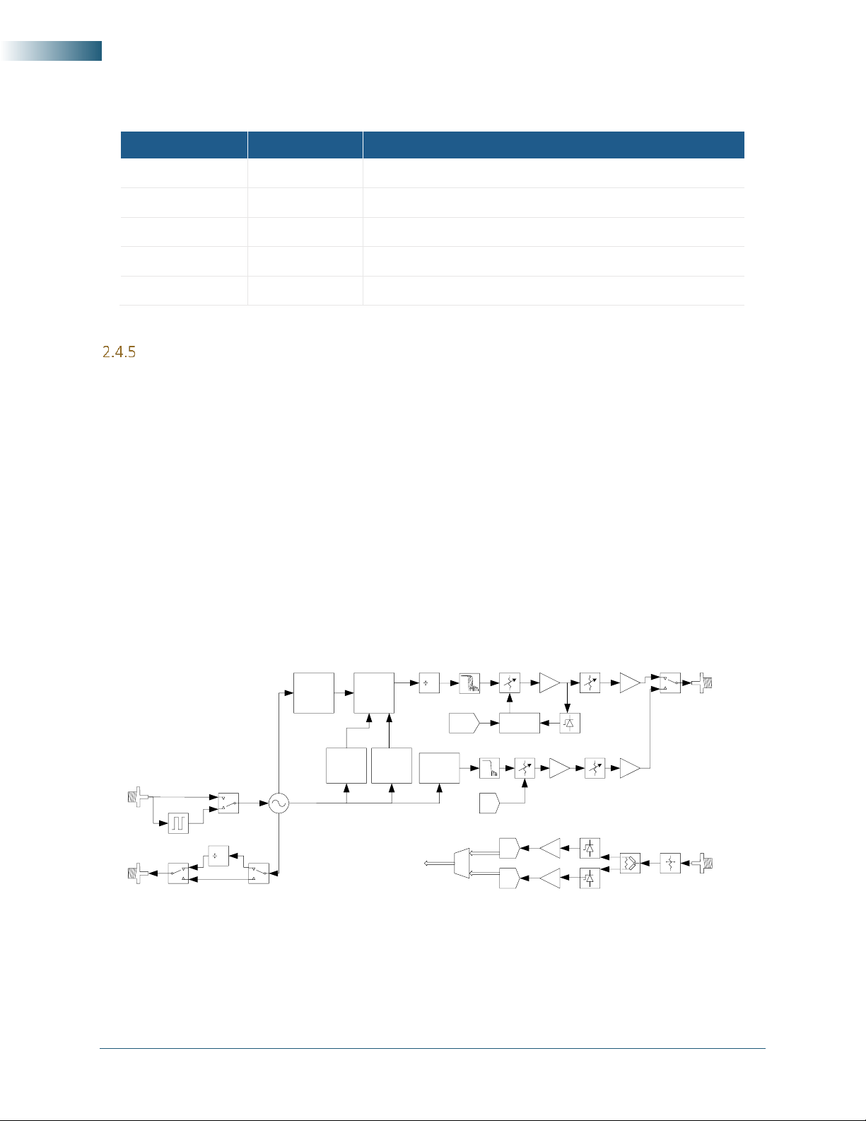
general-purpose lab source. Figure 3 shows the block diagram of the device, and the following subsections provide details of its operation.
Figure 3. PSG block diagram
N
Fine Step
Gen
REF
IN
REF
OUT
RF
OUT
2.9 GHz
GHz
Sum Gen
Harmonic
Coarse
Step Gen
DC-
50MHz
Gen
SENSOR
IN
VCXO
10
OCXO
25 MHz to 6.25 GHz path
ALC
controller
Filter
Bank
ADC
0
1
ADC
RMS
ENV
DC to 50 MHz path
VVA
VVA
60 dB
DSA
32 dB
DSA
HF ALC
DAC
LF
DAC
FracN
Coarse
Step Gen
Page 12

©2019 Rev 1.0
11
Theory and Operation
RF Generation
The PSG is a true DC to 6 GHz low phase noise, low harmonics, and low spur synthesizer that uses a
hybrid synthesizer architecture comprising of phase lock loops, harmonic generation, and DDS functions.
Coarse tuning is accomplished by PLL and harmonic generators, while fine tuning is accomplished with
the variable modulus DDS, providing exact frequency generation with resolution of 1 mHz. Isolation
between the internal oscillators, their mixed IF products, harmonics, and inter-modulation products is
accomplished by internal EMI sealed cavities, resulting in improved overall phase noise performance and
reduction of spurious signal content of this compact size frequency synthesizer. Synthesized signals
reference an internal 10 MHz OCXO clock, or an external 10 MHz reference.
Amplitude Control
The output level of the PSG is controlled through an automatic leveling control (ALC) circuitry. The ALC
can operate in close or open loop. The advantages of the close loop over the open loop operation are
that the power levels are more stable and accurate. The disadvantage of the close loop is that it increases
the AM noise of the carrier sideband. Although this AM noise is typically lower than the phase noise, it
may have impact on some applications. In such applications, it is best to operate the ALC in open loop.
Fine amplitude adjusts can be made by changing the ALC DAC value. Additionally, the ALC can be disabled
and output level can be adjusted manually using the RF attenuators. Disabling the ALC further improves
the AM noise because the internal voltage-variable attenuator is turned off, removing control voltage
noise to amplitude noise conversion.
Computational Time
The ALC control is accomplished by controlling the ALC DAC and the output step attenuator. The settings
of these two components are dynamically calculated based on the level required and a large set of
calibration values. Similarly, to change frequency would require four phase lock loops to be programmed
and their settings are dynamically calculated based on a set of calibration values. Due to the calculations
involved, computational time to set frequency change is typically 250 µs, and about 350 µs to compute
and set up the ALC.
For faster frequency changes, especially for sweeps less than a couple of 100 MHz, it is recommended
that the automatic leveling of the power be turned off. This will prevent the PSG from having to compute
a fresh set of the ALC parameters at each frequency point. Typically, the un-calibrated power level does
not change by more than a couple of dB over a 100 MHz range. See device register 0x14 for details on
turning on and off this automatic leveling feature.
RF Power Sensor
The RF power sensor frequency response is from 10 MHz to 6 GHz. Its amplitude response is -25 dBm to
20 dBm. The sensor may be used in transfer measurement applications….
Page 13

Rev 1.0 | SC5507A & SC5508A Hardware Manual SignalCore, Inc.
12
SC5507A & SC5508A Hardware Manual
Internal EEPROM
The PSG contains an EEPROM whose memory space is divided into calibration and operating data spaces.
The calibration data space contains device information such as serial number, hardware revision,
firmware revision, and production date. In addition, this space holds the calibration data for frequency
tuning and amplitude control. The operating data space contains the default startup configuration of the
device such as the single fixed tone mode frequency and sweep/list mode operation. It also holds the list
mode configuration parameters such as sweep behavior (saw or triangular waveform), software or
hardware trigger, start/stop/step frequencies, dwell time, sweep/list cycles, etc. Space is allocated for
2048 frequency points and 2048 corresponding amplitude points that the user may choose to store for
list mode operation. The internal EEPROM is not accessible for users to store data.
Modes of RF Generation
The PSG has both single fixed tone and list mode operation in frequency generation. In single fixed tone
mode, it operates as a normal synthesizer where the user writes the frequency (RF_FREQUENCY) register
to change the frequency. In list mode, the device is triggered to automatically run through a set of
frequency points that are either entered directly by the user or pre-computed by the device based on
user parameters. Configuration of the device for list mode operation is accomplished by setting up the
LIST_MODE_CONFIG register.
Sweep Function
When frequency points are generated based on the start/stop/step set of frequencies, this is (in the
context of this product) known as putting the device into sweep. When the sweep function is enabled,
the frequency points are incrementally stepped with a constant step size either in a linearly increasing or
linearly decreasing fashion.
List Function
The list function requires that the frequency points are read in from a list provided by the user. The user
will need to load the frequency points into the list buffer via the LIST_BUFFER_WRITE register, or have the
device read the frequency points from the EEPROM into it.
Sweep Direction
The sweep can be chosen to start at the beginning of a list and incrementally step to the end of the list or
vice versa.
Sweep Waveform
The list of frequency points may be swept in a sawtooth manner or triangular manner. If sawtooth is
selected, upon reaching the last frequency point the device returns back to the starting point. Plotting
frequency versus time reveals a sawtooth pattern. If triangular is selected, the device will sweep linearly
from the starting point, then reverse its direction after the last (highest or lowest) frequency and sweep
backwards toward the start point, mapping out a triangular waveform on a frequency versus time graph.
Page 14

©2019 Rev 1.0
13
Theory and Operation
Dwell Time
The dwell time at each frequency, in either sweep or list modes, is determined by writing to the
LIST_DWELL_TIME register. The dwell time step increment is 500 µs. However, the recommended
minimum dwell time is 1 ms, which allows sufficient time for the signal to settle before a measurement is
made. Due to the size limitation of the onboard RAM, it is not possible to have a pre-calculated
configuration parameters list that could be used to program the various functions of the device,
decreasing the setup time of the device for frequency change. As a result, for each frequency change the
configuration parameters are dynamically computed. This overhead computational time to handle the
mathematics, triggers, timers, and interrupts may increase the effective frequency settling time close to
500 µs. The amplitude computational time alone is close to 350 µs. If the sweep is over a narrow range, it
is best to disable the automatic power leveling feature, allowing faster frequency sweeps. By default,
whenever the frequency changes, the device re-computes a set of new parameters to set the ALC. Over
short range frequencies, the parameters are similar so the amplitude variation may be acceptable. If
automatic power leveling is turned on, allow for a minimal dwell time of 2-5 ms.
List Cycles
The number of repeat cycles for a sweep or list is set by writing the LIST_CYCLE_COUNT register. Writing
the value 0 to the register will cause the device to repeat the sweep/list forever until a trigger is sent or
the RF mode is changed to single fixed tone mode via the RF_MODE register. Upon completion of a cycle,
the frequency may be set to end on the last frequency point or return back to the starting point. This
cycle ending behavior is configured with bit [5] of the LIST_MODE_CONFIG register.
Trigger Sources
The device may be set up for software or hardware triggering. This is defined in bit [4] of the
LIST_MODE_CONFIG register. If software trigger is selected, writing the LIST_SOFT_TRIGGER register will
trigger the device to perform the sweep/list function defined in the LIST_MODE_CONFIG register. The
device may also be triggered via pin 21, the hardware trigger pin (TRIGIN). Hardware triggering occurs on
a high to low transition state of this pin. Note, hardware triggering is currently not available for the
SC5507A.
Hardware Trigger Modes
The device may be triggered to start a sweep or list then use the next trigger to stop it. In triggered
start/stop mode, alternating triggers will start and stop the sweep/list. In this mode, start triggering will
always return the frequency point to the beginning of the sweep/list. It does not continue from where it
left off from a stop trigger. The device may also be triggered to step to the next frequency with each start
trigger. This is known as the triggered step mode. Software triggering cannot perform the step trigger
function. This can only be done through hardware triggering. When hardware step triggering has started,
performing a software trigger or changing the RF mode to single fixed tone will take the device out of
step trigger state before a cycle is completed.
Trigger Out Modes
The device can be set to send out a high to low transition signal when the configuration of a frequency by
the device is completed; that is, it has completed all necessary computations, and has successfully written
Page 15

Rev 1.0 | SC5507A & SC5508A Hardware Manual SignalCore, Inc.
14
SC5507A & SC5508A Hardware Manual
data to the appropriate components. This trigger pulse can be sent on the completion of every step
frequency or on the last frequency of a sweep cycle. This trigger signal is present on pin 20 (TRIGOUT).
Default Startup Mode
The factory power-up state for the device is detailed in the following table. The default state can be
changed to the current state of either channel programmatically, allowing the user to power up the
device in the last saved state without having to reprogram.
Table 5. Factory Default Power-Up State.
RF Out
Frequency
3 GHz
Power
0.00 dBm
RF Output
Enabled
ALC Mode
Closed Loop
Standby
Disabled
Auto Level
Enabled
Ref Out Select
10 MHz
Ext Ref Lock
Disabled
4 Hardware Registers
Configuration Registers
These are write-only registers to configure the device. The registers vary in length to reduce redundant
data and improve the communication speed, especially for SPI and RS232 interfaces. Furthermore, it is
vitally important that the length of data written to a register is exact because failure to do so will cause
the interfaces to misinterpret the incoming data, leaving the device in a stalled state. The total number of
bytes is the sum of the register address (1 Byte) and its corresponding data bytes. For example, to set the
RF frequency value, eight bytes must be written; the sum of the 1 register byte and 7 data bytes. See the
RF_FREQUENCY register of Table 6. The table provides a summary of the configuration registers, and each
register is explained in detail in the sections following.
Table 6. Configuration Registers
Register Name
Register
Address
Serial
Range
Bit 7
Bit 6
Bit 5
Bit 4
Bit 3
Bit 2
Bit 1
Bit 0
INITIALIZE
0x01
[7:0]
Open
Open
Open
Open
Open
Open
Open
Mode
SYSTEM_ACTIVE
0x02
[7:0]
Open
Open
Open
Open
Open
Open
Open
Enable
‘active’
LED
Page 16

©2019 Rev 1.0
15
Hardware Registers
Register Name
Register
Address
Serial
Range
Bit 7
Bit 6
Bit 5
Bit 4
Bit 3
Bit 2
Bit 1
Bit 0
SYNTH_MODE
0x03
[7:0]
Open
Open
Open
Open
Open
Disable
SS
Loop
gain
Lock
mode
RF_MODE
0x04
[7:0]
Open
Open
Open
Open
Open
Open
Open
Mode
LIST_MODE_CONFIG
0x05
[7:0]
Trig
out
mode
Trig
out
enable
Return
to start
Step
on
trigger
Hw
trigger
Saw /
Tri
wave
Sweep
dir
SSSmode
LIST_START_FREQ
0x06
[55:0]
Frequency Word (mHz) [55:0]
LIST_STOP_FREQ
0x07
[55:0]
Frequency Word (mHz) [55:0]
LIST_STEP_FREQ
0x08
[55:0]
Frequency Word (mHz) [55:0]
LIST_DWELL_TIME
0x09
[31:0]
Dwell Word[31:0]
[39:32]
Set to Zeros
LIST_CYCLE_COUNT
0x0A
[31:0]
Count Word[31:0]
[39:32]
Set to Zeros
RESERVED
0x0B
[7:0]
Open
Open
Open
Open
Open
Open
Open
Mode
LIST_BUFFER_POINTS
0x0C
[15:0]
Points Word [15:0]
[23:16]
Set to Zeros
LIST_BUFFER_WRITE
0x0D
[55:0]
Frequency Word (mHz) [55:0] See
LIST_BUF_MEM_XFER
0x0E
[7:0]
Open
Open
Open
Open
Open
Open
Open
Mode
LIST_SOFT_TRIGGER
0x0F
[7:0]
Open
Open
Open
Open
Open
Open
Open
Open
RF_FREQUENCY
0x10
[55:0]
Frequency Word (mHz) [55:0]
RF_LEVEL
0x11
[7:0]
RF Power Word [7:0] in 100th dB
[15:0]
Sign Bit
RF Power Word [14:8] in 100th dB
[23:16]
Set to Zeros
RF_OUT_ENABLE
0x12
[7:0]
Open
Open
Open
Open
Open
Open
Open
Mode
RF_PHASE
0x13
[23:0]
RF_PHASE Word [23:0] (in 100th of deg)
[31:24]
Zero
RF_PHASE Word [30:24] (in 100th of deg)
AUTO_LEVEL_DISABLE
0x14
[7:0]
Open
Open
Open
Open
Open
Open
Open
Mode
RF_ALC_MODE
0x15
[7:0]
Open
Open
Open
Open
Open
Open
Open
Mode
RF_STANDBY
0x16
[7:0]
Open
Open
Open
Open
Open
Open
Open
Mode
REFERENCE_MODE
0x17
[7:0]
Open
Open
Open
Open
Open
Open
Ref
Out
Select
Lock
Enable
REFERENCE_DAC_SETTING
0x18
[7:0]
DAC Word [7:0]
[15:8]
Open
Open
DAC Word [13:8]
[23:16]
Zeros
ALC_DAC_VALUE
0x19
[7:0]
DAC Word [7:0]
[15:8]
Open
Open
DAC Word [13:8]
[23:16]
Zeros
DIRECT_ATTEN_CNTRL
0x1A
[7:0]
32
16 (dB)
8 4 2 1 .5
0.25
[15:8]
[15:9] Zeros
Atten
Select
[23:16]
Zeros
STORE_DEFAULT_STATE
0x1B
[7:0]
Open
Open
Open
Open
Open
Open
Open
Open
SELF_SYTHN_CAL
0x1C
[7:0]
Open
Open
Open
Open
Open
Open
Open
Select
Synth
Page 17

Rev 1.0 | SC5507A & SC5508A Hardware Manual SignalCore, Inc.
16
SC5507A & SC5508A Hardware Manual
Register Name
Register
Address
Serial
Range
Bit 7
Bit 6
Bit 5
Bit 4
Bit 3
Bit 2
Bit 1
Bit 0
SENSOR SETTING
0x1D
[7:0]
Open
Open
Open
Open
Open
Open
Open
Open
SENSOR FREQ
0x1E
[55:0]
Open
Open
Open
Open
Open
Open
Open
Open
RESERVED
0x1F
[7:0]
Each register from the table above is explained in detail in the following subsections.
Register 0x01 INITIALIZE (1 Byte)
This register allows the user to re-initialize the device with current settings or to the power up state.
Bit
Type
Name
Width
Description
[0]
WO
Mode
1
0 = Re-initialize device with current settings
1 = Re-initialize device to power up state
[7:1]
WO
Unused
7
Set all bits to zero
Register 0x02 SET_SYS_ACTIVE (1 Byte)
This register turns on or off the active LED indicator on the front connector interface of the device. This
register should be called when the device is opened or closed in software.
Bit
Type
Name
Width
Description
[0]
WO
Mode
1
0 = turns off the active LED
1 = turns on the active LED
[7:1]
WO
Unused
7
Set all bits to zero
Register 0x03 SYNTH_MODE (1 Byte)
This register configures the PLL loop gain of the local oscillator synthesizers. It also enables or disables
faster tuning of the YIG based oscillator of LO1.
Bit
Type
Name
Width
Description
[0]
WO
Lock Mode
2
0 = harmonic offset mode
1 = fracN PLL offset mode
[1]
WO
Loop Gain
2
0 = Normal loop gain for better close in phase
noise
1 = Low loop gain for better far out phase noise
and spur suppression
[2]
WO
Disable spur
suppression
1
Only applies in harmonic offset mode, see bit [0].
Page 18

©2019 Rev 1.0
17
Hardware Registers
Bit
Type
Name
Width
Description
0 = The device automatically switches to fracN
offset mode to avoid potentially large spurs due
to intermodulation between the carrier and the
harmonics of the reference clock.
1 = This disables the function and may speed up
tuning speed in some cases
[3]
WO
Force low path
1
0 = Use lower frequency generator for
frequencies < 25 MHz
1 = Use lower frequency generator for
frequencies ≤ 50 MHz
[4]
WO
Unused
1
0 = set the phase of signal to 0 of Cos(x)
1 = phase continues from last non-DC CW signal
(only for previous frequency < 50 MHz from low
frequency generator)
[7:5]
WO
Unused
3
Set all bits to zero
Register 0x04 RF_MODE (1 Byte)
This register controls the single fixed tone mode and sweep / list mode.
Bit
Type
Name
Width
Description
[0]
WO
RF Mode
1
0 = Single fixed tone mode. This mode must be
set to change the frequency value via register
0x1A
1 = Sweep / list mode. In this mode, writing to
register 0x10 will be unresponsive. This register
must be called first for sweep / list triggering to
function
[7:1]
WO
Unused
7
Set all bits to zero
Page 19

Rev 1.0 | SC5507A & SC5508A Hardware Manual SignalCore, Inc.
18
SC5507A & SC5508A Hardware Manual
Register 0x05 LIST_MODE_CONFIG (1 Byte)
This register controls the list mode configurations.
Bit
Type
Name
Width
Description
[0]
WO
SSS Mode
1
0 = List mode. Device gets its frequency points
from the list buffer uploaded via the
LIST_BUFFER_WRITE register (0x0D).
1 = Sweep mode. The device computes the
frequency points using the Start, Stop, and Step
frequencies.
[1]
WO
Sweep Direction
1
0 = Forward. In the forward direction, the sweeps
start from either the lowest start frequency or
the beginning of the list buffer.
1 = Reverse. In the reverse direction, the sweep
starts with the stop frequency and steps down
toward the start frequency or starts at the end
and steps toward the beginning of the buffer.
[2]
WO
Triangular
Waveform
1
0 = Sawtooth waveform. Frequency returns to
the beginning frequency upon reaching the end
of a sweep cycle.
1 = Triangular waveform. Frequency reverses
direction at the end of the list and steps back
towards the beginning to complete a cycle.
[3]
WO
Soft/Hardware
Trigger
1
0 = Software trigger. Software trigger can only be
used to start and stop a sweep/list cycle. It does
not work for step-on-trigger mode.
1 = Hardware trigger. A high-to-low transition on
the TRIGIN pin will trigger the device. It can be
used for both start/stop or step-on-trigger
functions
Page 20

©2019 Rev 1.0
19
Hardware Registers
Bit
Type
Name
Width
Description
[4]
WO
Step on Trigger
1
0 = Start/Stop behavior. The sweep starts and
continues to step through the list for the number
of cycles set, dwelling at each step frequency for
a period set by the LIST_DWELL_TIME register.
The sweep/list will end on a consecutive trigger.
1 = Step-on-trigger. This is only available if
hardware triggering is selected. The device will
step to the next frequency on a trigger. Upon
completion of the number of cycles (set by the
LIST_CYCLE_COUNT register), the device will exit
from the stepping state and stop. Further
triggering will set the device back into the
stepping state. To exit the stepping state and
stop before reaching the end of a cycle, a
software trigger must be sent or a change in the
RF mode to single fixed tone needs to be made.
[5]
WO
Return to Start
1
0 = Stop at end of sweep/list. The frequency will
stop at the last point of the sweep/list.
1 = Return to start. The frequency will return and
stop at the beginning point of the sweep or list
after a cycle.
[6]
WO
Trigger Output
1
0 = No trigger output.
1 = Puts a trigger pulse on the TRIGOUT pin
[7]
WO
Trigger Out Mode
1
0 = Puts out a trigger pulse at each frequency
change, right after all internal devices are
configured.
1 = Puts out a trigger pulse at the completion of
each sweep/list cycle.
Register 0x06 LIST_START_FREQ (7 Bytes)
This register sets the start frequency for a sweep.
Bit
Type
Name
Width
Description
[55:0]
WO
List Start
Frequency
56
Sets the start frequency for a sweep. Start
frequency should always be lower than the stop
frequency. The Sweep Direction bit [1] of register
0x05 should be used to determine where the
sweep should begin.
Page 21

Rev 1.0 | SC5507A & SC5508A Hardware Manual SignalCore, Inc.
20
SC5507A & SC5508A Hardware Manual
Register 0x07 LIST_STOP_FREQ (7 Bytes)
This register sets the stop frequency for a sweep.
Bit
Type
Name
Width
Description
[55:0]
WO
List Stop
Frequency
56
Sets the stop frequency for a sweep. Stop
frequency should always be higher than the start
frequency.
Register 0x08 LIST_STEP_FREQ (7 Bytes)
This register sets the list step frequency.
Bit
Type
Name
Width
Description
[55:0]
WO
List Step
Frequency
56
Sets the step frequency for a sweep. Step size
should not exceed the difference between the
start and stop frequencies.
Register 0x09 LIST_DWELL_TIME (7 Bytes)
This register sets the dwell time at each step frequency.
Bit
Type
Name
Width
Description
[31:0]
WO
List Dwell Time
32
Set the dwell time at each step frequency. The
Dwell time is incremented in 500 s increments.
For example, to produce a 10 ms dwell time the
value written to this register is 20d.
[55:32]
WO
Unused
24
Set to zeros
Register 0x0A LIST_CYCLE_COUNT (7 Bytes)
This register sets the device to cycle forever.
Bit
Type
Name
Width
Description
[31:0]
WO
List Cycle Count
32
0 = Cycle forever. This will set the device to cycle
forever. Any number greater than 0 will set the
number of cycles the device will sweep or step
through the list then stop. This applies for both
start / stop and step trigger modes.
[55:32]
WO
Unused
24
Set to zeros
Page 22

©2019 Rev 1.0
21
Hardware Registers
Register 0x0B Reserved
Bit
Type
Name
Width
Description
[7:0]
WO
Reserved
7
Register 0x0C LIST_BUFFER_POINTS (3 Bytes)
This register sets the number of frequency points to step through in the buffer list.
Bit
Type
Name
Width
Description
[15:0]
WO
Number of Buffer
Points
16
Sets the number of frequency points to step
through in the buffer list. The number must be
equal to or less than the buffer length. This
number will overwrite the count determined
from the LIST_BUFFER_WRITE register.
[23:16]
WO
Unused
8
Set to zeros
Register 0x0D LIST_BUFFER_WRITE (7 Bytes)
This register stores the frequency and amplitude points into the list buffer held in RAM. Data must be
entered as sequential pairs of frequency followed by amplitude.
Bit
Type
Name
Width
Description
[54:0]
WO
Buffer word
Frequency or
amplitude
55
Writing this register stores the frequency (mHz)
or amplitude (100th of dBm) point into the list
buffer held in RAM.
Writing 0x0000000000 to this buffer resets the
pointer to buffer location [0] and flags the device
to store data written to this register. Consecutive
non-zero writes to this register will increase the
buffer counter up to 2047. Further writes beyond
this point are not recognized. Writing
0x7FFFFFFFFF to this register, and [55] = 1, at any
time will terminate the write process and stops
the pointer increment. The value at which the
pointer stops is the new count of list frequency
points unless it is overwritten by register
LIST_BUFFER_POINTS.
[55]
WO
Frequency or
amplitude
1
0 = indicates that the bits 54:0 buffer is
frequency
1 = indicates that the buffer is amplitude
Page 23

Rev 1.0 | SC5507A & SC5508A Hardware Manual SignalCore, Inc.
22
SC5507A & SC5508A Hardware Manual
Register 0x0E LIST_BUF_MEM_TRNSFER (1 Byte)
This register transfers data between EEPROM memory and the list buffer (in RAM).
Bit
Type
Name
Width
Description
[0]
WO
Transfer Direction
1
0 = Transfers the contents of the list buffer into
EEPROM memory. The size of the transfer is set
by the list frequency points.
1 = Transfers the contents from EEPROM
memory to the list buffer (in RAM).
[7:1]
WO
Unused
7
Set all bits to zero
Register 0x0F LIST_SOFT_TRIGGER (1 Byte)
This register provides a soft trigger to the device.
Bit
Type
Name
Width
Description
[7:0]
WO
Soft Trigger
8
Set all bits to zero. Calling this register provides a
soft trigger to the device.
Register 0x10 RF_FREQUENCY (7 Bytes)
This register sets the RF1 frequency.
Bit
Type
Name
Width
Description
[55:0]
WO
RF1 Frequency
Word
56
Sets the RF frequency in mHz
Register 0x11 RF_LEVEL (3 Bytes)
This register sets the RF1 power level.
Bit
Type
Name
Width
Description
[14:0]
WO
RF1 Power Level
15
Sets the RF1 Power level in hundreds of dB. To
set to 10.25 dB, write 1025 to this register
[15]
WO
Sign bit
1
0 = Positive number
1 = Negative number
[23:16]
WO
Unused
8
Zeros
Page 24

©2019 Rev 1.0
23
Hardware Registers
Register 0x12 RF_ENABLE (1 Byte)
This register enables and disables the RF1 output power.
Bit
Type
Name
Width
Description
[0]
WO
RF1 Enable
1
0 = Disables the output power
1 = Enables the output power
[7:1]
WO
Unused
7
Set all bits to zero
Register 0x13 RF_PHASE (7 Bytes)
This register sets the phase word.
Bit
Type
Name
Width
Description
[30:0]
WO
Phase word
31
Phase word in hundredths of a degree
[31]
WO
Reserved
1
Set to 0
[55:32]
Unused
24
Set to zeros
Register 0x14 AUTO_LEVEL_DISABLE (1 Byte)
This register enables and disables the RF amplifier.
Bit
Type
Name
Width
Description
[0]
WO
RF1 Auto leveling
1
0 = Power is leveled on frequency change
1 = Power is not leveled on frequency change
with explicitly calling register 0x11 (RF_LEVEL)
[7:1]
W
Unused
7
Set all bits to zero
Register 0x15 RF_ALC_MODE (1 Byte)
This register corrects the amplitude using closed or opened loops.
Bit
Type
Name
Width
Description
[0]
WO
RF1 ALC Mode
1
0 = Amplitude is corrected using ALC closed loop
1 = Amplitude is corrected using ALC opened loop
[7:1]
WO
Unused
7
Set all bits to zero
Page 25

Rev 1.0 | SC5507A & SC5508A Hardware Manual SignalCore, Inc.
24
SC5507A & SC5508A Hardware Manual
Register 0x16 RF_STANDBY (1 Byte)
This register puts the RF1 channel into standby, reducing power consumption.
Bit
Type
Name
Width
Description
[0]
WO
RF1 Standby
1
1 = Puts the RF1 channel into standby. Standby
powers down all circuitry associated with ch1,
thus reducing power consumption.
[7:1]
WO
Unused
7
Set all bits to zero
Register 0x17 REFERENCE_MODE (1 Byte)
This register tells the device to lock to an external reference source.
Bit
Type
Name
Width
Description
[0]
WO
Lock to external
reference source
1
1 = instructs the device to lock to external
source. No attempt will be made unless a
reference source is detected.
[1]
WO
Reference out
select
1
0 = Outputs a 10 MHz signal
1 = Outputs a 100 MHz signal
[7:2]
WO
Unused
6
Set all bits to zero
Register 0x18 REFERENCE_DAC_VALUE (3 Bytes)
This register allows the user to set or adjust the internal 10 MHz TCXO frequency.
Bit
Type
Name
Width
Description
[13:0]
WO
DAC Value
14
14 bit word to set/adjust the internal 10 MHz
TCXO frequency
[23:14]
WO
Unused
10
Set all bits to zero
Register 0x1A DIRECT_ATTEN
This register allows the user to set the LF or HF attenuators manually, thus overriding calibrated values.
Bit
Type
Name
Width
Description
[7:0]
WO
Value
8
0.25 dB LSB for RF attenuators up to 63.75 dB, 1
dB LSB for LF attenuators up to 32 dB.
[8]
WO
Atten select
1
0 = RF attenuators
1 = LF attenuators
Page 26

©2019 Rev 1.0
25
Hardware Registers
[23:9]
WO
Unused
15
Set to zeros
Register 0x1B STORE_DEFAULT_STATE (1 Byte)
This register stores the current configuration into memory.
Bit
Type
Name
Width
Description
[7:0]
WO
Reserved
8
Set all bits to zero. Calling this register will store
the current configuration into memory. On reset
or power-up these values are read from memory
and set as the default values.
Register 0x1C SELF_SYNTH_CAL (1 Byte)
This register turns on self-calibration of 2 internal synthesizers.
Bit
Type
Name
Width
Description
[0]
WO
Select Synth
1
0 = auto calibrates the coarse frequency VCO
1 = auto calibrates the fine VCO
[7:1]
WO
Unused
7
Set to Zeros
Register 0x1D SENSOR_SETTING (3 Byte)
This register sets up the power sensor.
Bit
Type
Name
Width
Description
[0]
WO
Sensor Enable
1
Enables sensor
[1]
WO
Sensor Mode
1
0 = RMS detection mode
1 = Envelope detection mode
[7:2]
WO
Unused
6
Set to zeros
[23:8]
WO
Number of
averages per read
16
Number averages
Page 27

Rev 1.0 | SC5507A & SC5508A Hardware Manual SignalCore, Inc.
26
SC5507A & SC5508A Hardware Manual
Register 0x1E SENSOR_FREQUENCY (7 Byte)
This register provides the frequency at which measurement correction is applied.
Bit
Type
Name
Width
Description
[55:0]
WO
Frequency (mHz)
56
Frequency word[55:0]
Query Registers
These are request for data registers, in that a request for certain data is made by writing to the specific
register first, and then followed by reading back the requested data. Some registers may require instruction
data to specify the type of data to return, while others do not need any. For example, the
GET_RF_PARAMETERS (0x20) returns sweep dwell time, rf1_frequency, rf2_frequency, etc; this depends
on the request instruction byte.
Returned data length is always 8 bytes (64 bits), with the first byte being the most significant (MSB). Not all
8 bytes are valid, some have 7, some 4, and others 2. It is important that all 8 bytes are read in order to
clear the interface buffers.
Table 7. Query Registers
Register Name
Register
Address
Serial
Range
Bit 7
Bit 6
Bit 5
Bit 4
Bit 3
Bit 2
Bit 1
Bit 0
FETCH_RF_PARAMETERS
0x20
[7:0]
Open
Open
Open
Open
Parameter
FETCH_TEMPERATURE
0x21
[7:0]
Open
Open
Open
Open
Open
Open
Open
Open
RETCH_DEVICE_STATUS
0x22
[7:0]
Open
Open
Open
Open
Open
Open
Open
Open
FETCH_DEVICE_INFO
0x23
[7:0]
Info
FETCH_LIST_BUFFER
0x24
[7:0]
Buffer Address [7:0]
[15:8]
Zeros [15:12]
Buffer Address [11:8]
[23:16]
Zeros [23:16]
FETCH_DAC_VALUE
0x25
[7:0]
Zeros[7:1]
DAC
Select
SERIAL_OUT_BUFFER
0x26
[7:0]
Zeros [7:0]
RESERVED
0x27
[7:0]
FETCH_SENSOR_VALUE
0x28
[7:0]
Zeros [7:0]
Page 28

©2019 Rev 1.0
27
Hardware Registers
Register 0x20 GET_RF_PARAMETERS (1 Byte sent, 8 Bytes received)
Write to this register the required RF parameter to query from the device.
Bit
Type
Name
Width
Description
[3:0]
WO
Parameter
4
Data specifies the parameter to retrieve:
0x00 = Current RF Freq (7 valid bytes return)
0x01 = Sweep Start Freq (7 valid bytes return)
0x02 = Sweep Stop Freq (7 valid bytes return)
0x03 = Sweep Step Freq (7 valid bytes return)
0x04 = Sweep Dwell Time (4 valid bytes return)
0x05 = Sweep Cycle Count (4 valid bytes return)
0x06 = Sweep List Buffer Pts (4 valid bytes return)
0x07 = Current RF Phase (4 valid bytes return*)
0x08 = Current RF Level (4 valid bytes return*)
0x09 = Current Sensor Freq (7 Valid bytes)
0x0A = Sensor ADC value (2 valid bytes)
(*) is 4 bytes of a float format number, for
example:
float phase=*(float*)&read_in_unsigned_int
[7:4]
WO
Unused
4
Set all bits to zero
[63:0]
RO
Data
64
Data with varying sizes of unsigned type
Register 0x21 GET_TEMPERATURE (1 Byte, 8 Bytes)
Write to this register to query the device temperature.
Bit
Type
Name
Width
Description
[7:0]
WO
Unused
8
Set all to zero
[31:0]
RO
Valid flatten float
type temperature
32
The data is returned in unsigned integer form of
flatten float type. To recast the unsigned integer
back to float use:
float temp = *(float*)&read_in_unsigned_int_var
[63:32]
RO
Invalid data
32
zeros
Page 29

Rev 1.0 | SC5507A & SC5508A Hardware Manual SignalCore, Inc.
28
SC5507A & SC5508A Hardware Manual
Register 0x22 GET_DEVICE_STATUS (1 Byte, 8 Bytes)
Write to this register to query the current operating conditions.
Bit
Type
Name
Width
Description
[7:0]
WO
Unused
8
Set all bits to zero. Sets up the read-back buffer
with contents of the current device status.
Contents are immediately available for USB read.
The contents occupy effectively the lower two
bytes. In the case of SPI, contents are transferred
to the serial output buffer, so a second query to
the SERIAL_OUT_BUFFER register is required to
transfer its contents and also to clear the output
buffer.
[63:32]
RO
Invalid data
32
[31]
RO
List Config: Trig Out
Mode
1
0 = trigger once on each step
1 = trigger once on each cycle
[30]
RO
List Config: Trig Out
Enable
1
1 = trigger pulse at trigger out pin
[29]
RO
List Config: Return
to Start
1
0 = list ends at the end of a list
1 = if list ends and cycles completed, pointer
returns to start.
[28]
RO
List Config: Step
Trig
1
0 = HW trigger starts and stops the list
1 = HW trigger steps the list points
[27]
RO
List Config: HW Trig
1
0 = SW trigger
1 = HW trigger
[26]
RO
List Config:
Waveform (Tri/Saw)
1
0 = list steps start to stop then traces the steps
back to start.
1 = list steps start to stop and return immediately
to start
[25]
RO
List Config: Sweep
Dir
1
0 = start to stop
1 = stop to start
[24]
RO
List Config: SSS
mode
1
0 = uses list points calculated using the start, stop,
and step frequencies.
1 = uses the list points entered manually
[31:28]
RO
Reserved
4
[27]
RO
Operate: device
accessed
1
0 = no host in communication with device
1 = the device has opened communication with
host
[26]
RO
Operate:
Over_temp
1
0 = temperature is within operation range
1 = temperature of device is too high
[25]
RO
Operate: Ext. ref
detect
1
0 = no reference source detected
1 = reference source detected
Page 30

©2019 Rev 1.0
29
Hardware Registers
Bit
Type
Name
Width
Description
[24]
RO
Operate: List mode
running
1
0 = list mode not running
1 = list mode is running
[23]
RO
Operate: RF Mode
1
0 = CW mode
1 = List mode
[22]
RO
Operate: sensor
mode
1
0 = RMS mode
1 = Envelope mode
[21]
RO
Operate: sensor
enable
1
Enable reading of power sensor
[20]
RO
Operate: synth
standby
1
0 = synth operates normally
1 = synthesizer is powered down
[19]
RO
Operate: Pulse
enable
1
0 = direct pulse of the output switch is off
1 = control of switch via I/O port is enabled
[18]
RO
Operate: Auto level
adjust
1
0 = adjustment of amplitude is not applied upon
frequency change
1 = adjustment is made
[17]
RO
Operate: ALC open
1
0 = ALC loop is closed
1 = ALC loop is operating in open mode
[16]
RO
Operate: RF enable
1
1 = enable RF output signal
[15]
RO
Operate: PXI 10
MHz clock enable
1
0 = disable
1 = enable PXI clock at MCX port
[14]
RO
Operate: Ref clock
out select
1
0 = 10 MHz
1 = 100 MHz
[13]
RO
Operate: lock
external
1
0 = disabled
1 = enable
[12]
RO
Operate: cont dc
phase
1
0 = phase at DC is 0
1 = phase at DC continues from previous AC
[11]
RO
Operate: force low
freq path
1
1 = enable
[10]
RO
Operate: spur
suppresion
1
1 = enable
[9]
RO
Operate: loop_gain
1
0 = normal
1 = low loop gain
[8]
RO
Operate:
lock_mode
1
0 = harmonic
1 = fracN
[7]
RO
Unused
1 [6]
RO
Pll_status:ref_OCXO
1
1 = the 10 MHz OCXO is locked
[5]
RO
Pll_status:ref_VCXO
1
1 = the 100 MHz VCXO is locked
Page 31

Rev 1.0 | SC5507A & SC5508A Hardware Manual SignalCore, Inc.
30
SC5507A & SC5508A Hardware Manual
Bit
Type
Name
Width
Description
[4]
RO
Pll_status:crs_aux
1
1 = the auxiliary crs loop (fracN lock) is locked
[3]
RO
Pll_status:crs_ref
1
1 = the ref source for the crs loop is locked
[2]
RO
Pll_status:fine
1
1 = the DDS based fine loop is locked
[1]
RO
Pll_status:crs
1
1 = the crs (harmonic) loop is locked
[0]
RO
Pll_status:sum
1
1 = the main loop is locked
Register 0x23 GET_DEVICE_INFO (1 Byte, 8 Bytes)
Write to this register to query the device information such as serial number.
Bit
Type
Name
Width
Description
[2:0]
WO
Device Status
3
Writing this register will place the requested contents
into the output buffer. Contents are immediately
available for USB read. The contents occupy
effectively four bytes. In the case of SPI, contents are
transferred to the serial output buffer, so a second
query to the SERIAL_OUT_BUFFER register is required
to transfer its contents and also to clear the output
buffer.
0 = Obtain the product serial number
1 = Obtain the hardware revision
2 = Obtain the firmware revision
3 = Obtain the manufacture date
[7:3]
WO
Unused
5
[31:0]
RO
data
32
Data for the requested parameter:
Product Serial Number – 32-bit unsigned
Hardware Revision – typecast to 32-bit float
Firmware Revision – typecast to 32-bit float
Manufacture Date – unsigned 32-bit with following
[31:24] Year (last two digits)
[23:16] Month
[15:8] Day
[7:0] Hour
Page 32

©2019 Rev 1.0
31
Hardware Registers
Bit
Type
Name
Width
Description
[63:32]
RO
Invalid Data
32
Register 0x24 GET_LIST_BUFFER (3 Bytes, 8 Bytes)
Write to this register to query 8 bytes of data from the calibration EEPROM at the starting address.
Bit
Type
Name
Width
Description
[15:0]
WO
Buffer Address
16
The data point (0 – 2047) to read.
[22:16]
WO
Unused
7
[23]
WO
Select
1
0 = frequency
1 = amplitude
[63:0]
RO
Data
64
If frequency, data [63:0] is frequency in mHz
If amplitude, data is amplitude in the following format
[14:0] is absolute amplitude in 100th of dBm
[15] is the sign; 0 = pos, 1 = neg
[63:16] is invalid
Register 0x25 FETCH_DAC_VALUE (1 Byte, 8 Bytes)
Write to this register to query 8 bytes of data from the user EEPROM at the starting address.
Bit
Type
Name
Width
Description
[0]
WO
Dac select
1
0 is high frequency synth ALC DAC value
1 is low frequency synth amplitude DAC value
[7:1]
WO
Used
15
zeros
[15:0]
RO
Dac Value
16
Data
[63:16]
RO
Invalid Data
48
zeros
Register 0x26 SERIAL_OUT_BUFFER
Writing to this register only provides the 64 clock edges (Reg + 7 data bytes) to transfer serial data from
the device through SPI. Other interfaces do not use this register.
Bit
Type
Name
Width
Description
[63:0]
WO
Serial Out
Buffer
64
Set all bits to zero. Use of this register is only available
for the SPI interface.
[63:0]
RO
Request Data
64
The data clocked back is the contents requested by the
0x20 to 0x27 registers.
Page 33

Rev 1.0 | SC5507A & SC5508A Hardware Manual SignalCore, Inc.
32
SC5507A & SC5508A Hardware Manual
Section 2
Communication Interfaces
Page 34

©2019 Rev 1.0
33
Communication Interfaces
5 Communication Interfaces
The SC5507A has a PXI express interface, while the SC5508A has 2 communication interfaces:
1. USB and SPI
2. USB and RS232
This section will examine the communication aspects of the product, focusing on data transfer to and
from the device on each interface. Although the registers are identical for all interfaces, there are subtle
differences in the implementation of the interfaces to transfer the data.
Communication Data Format
All data sent and received by all interfaces is sent as buffers of unsigned bytes. For example, to change RF
frequency of the device to 3 GHz we perform the following:
1. Frequency is sent in 1000
th
of Hertz, so the data that represents the frequency is
3,000,000,000,000 milli-Hertz.
2. This number can be represented by a 64-bit unsigned long, and in Hexadecimal is 0x 0000 0574
FBDE 6000. The least 7 bytes are necessary to represent all frequencies allowable for this device,
so the MSB is used to hold the register address.
3. A buffer needs to be 8 bytes for register RF_FREQUENCY (address 0x10), so the byte array buffer
to be sent would be:
[0x10][0x00][0x05][0x74][0xFB][0xDE][0x60][0x00]
The register address byte [0x10] is the first member (MSB) of the buffer to be sent.
USB Interface
There are 2 transfer types for the USB interface.
• Control transfer
• Bulk transfer
Control Transfer
The USB control transfer parameters are:
ENDPOINT_IN
0x80
ENDPOINT_OUT
0x00
TYPE_VENDOR
0x40
RECIP_INTERFACE
0x01
Bulk Transfer
The USB bulk transfer parameters are:
ENDPOINT_IN
0x81
ENDPOINT_OUT
0x02
Page 35

Rev 1.0 | SC5507A & SC5508A Hardware Manual SignalCore, Inc.
34
SC5507A & SC5508A Hardware Manual
The bulk transfer from the host to the device operates on a loopback with a data buffer of 8 bytes. When
a device register is addressed, and upon completion of the register task, such as changing frequency, it
will send back 8 bytes, which the host must read to clear the transfer buffers. Unlike the other interface
methods, where only the required number of bytes needs to be sent for a given register, 8 bytes are
needed for every USB bulk transfer. For example, if a configuration register requires only 4 bytes to be
sent, these bytes will be the first of the 8 bytes and the last 4 bytes are zeros. The returned 8 bytes do not
carry valid data for a configuration register. However, they do carry valid data for query registers.
SPI Interface
The SPI interface on the device is implemented using an 8-bit (single Byte) buffer for both the input and
output, hence, it needs to be read and cleared by the device before consecutive bytes can be transferred
to and from it. The process of clearing the SPI buffer and decisively moving it into the appropriate register
takes CPU time, so a time delay is required between consecutive bytes written to or read from the device
by the host. The chip-select pin (𝐶𝑆
) must be asserted low before data is clocked in or out of the product.
Furthermore, pin 𝐶𝑆 must be asserted low for the entire duration of a register transfer.
Once a full transfer has been received, the device will proceed to process the command and de-assert low
the SRDY pin. The status of this pin may be monitored by the host because when it is de-asserted low, the
device will ignore any incoming data. The device SPI is ready when the previous command is fully
processed and the SRDY pin is re-asserted high. It is important that the host either monitors the SRDY pin
or waits for 500 𝜇𝑠 between register writes.
There are 2 SPI modes: 0 and 1. The default mode is 1, where data is clocked in and out of the device on
the falling edge of the clock signal. In mode 0, data is clocked in and out on the rising edge. To select
mode 0, pin 23 of the interface connector must be pulled low to ground as the device is powered on or as
the reset line (pin 19) is toggled low-high. If pin 23 is pulled high or left unconnected, mode 1 is selected.
Figure 4. SPI Mode 1 shown.
Register writes are accomplished in a single write operation. Register lengths vary depending on the
register. They vary in lengths of 2 to 8 bytes, with the first byte sent being the register address followed
by the data associated with that register. The (𝐶𝑆) pin must be asserted low for a minimum period of 1 𝜇𝑠
(Ts, see Figure #) before data is clocked in, and must remain low for the entire register write. The clock
rate may be as high as 5.0 MHz (Tc = 0.2 𝜇𝑠), however, if the external SPI signals do not have sufficient
integrity due to trace issues, the rate should be lowered.
MSB
CS
MISO
MOSI
CLK
MSB
LSB
LSB
Page 36

©2019 Rev 1.0
35
Communication Interfaces
Figure 5. SPI timing.
As mentioned above, the SPI architecture limits the byte rate since after every byte transfer the input and
output SPI buffers need to be cleared and loaded respectively by the device SPI engine. Data is
transferred between the input buffer and internal register buffers. The time required to perform this task
is indicated by 𝑇𝐵, which is the time interval between the end of one byte transfer and the beginning of
another. The recommended minimum time delay for 𝑇𝐵 is 1 𝜇𝑠. The number of bytes transferred
depends on the register. It is important that the correct number of bytes is transferred for the associated
register, because once the first byte (MSB) containing the device register address is received, the device
will wait for the desired number of associated data bytes. The device will hang if an insufficient number of
bytes are written to the register. To clear a hung condition, the device will need an external hard reset.
The time required to process a command is also dependent on the command itself. Measured times for
command completions are typically between 50 𝜇𝑠 to 300 𝜇𝑠 after reception.
Writing the SPI Bus
The SPI transfer size (in bytes) depends on the register being targeted. The first byte sent is the register
address and subsequent bytes contain the data associated with the register. As data from the host is
being transferred to the device via the MOSI line, data present on its SPI output buffer is simultaneously
transferred back, MSB first, via the MISO line. The data returned is invalid for configuration registers. The
following figure shows the contents of a single 3-byte SPI command written to the device. The Hardware
Registers section provides information on the number of data bytes and their contents for an associated
register. There is a minimum of 1 data byte for each register even if the data contents are “zeros”.
Figure 6. Example of a 3-byte write
Reading the SPI Bus
Data is simultaneously read back during a SPI transfer cycle. Requested data from a prior command is
available on the device SPI output buffers, and these are transferred back to the user host via the MISO
pin. To obtain valid requested data would require querying the SERIAL_OUT_BUFFER, which requires 8
bytes or 64 clock cycles; 1 byte for the device register (0x37) and 7 empty bytes (MOSI) to clock out the
returned data (MISO). An example of reading the device RF parameters (IF3 frequency) from the device is
shown in the following figure.
T
S
T
B
T
C
8 Bit Command/ Reg. Address
Byte N (MSB)
Byte N-1 (LSB)
CLK
DATA
CS
23 15 7 0
Register Address Byte 1 Byte 0
Page 37

Rev 1.0 | SC5507A & SC5508A Hardware Manual SignalCore, Inc.
36
SC5507A & SC5508A Hardware Manual
Figure 7. Query example: Write followed by Read to the GET_SERIAL_BUFFER
In the figure above, the first transfer cycle is to make the request for IF3 frequency data through the
GET_DEVICE_PARAM register. The subsequent cycle is to clock the data that was requested by sending 64
clocks into the GET_SERIAL_BUFFER register.
RS232 Interface
The RS232 version of the SC5508A has a standard interface buffered by an RS232 transceiver so that it
may interface directly with many host devices, such as a desktop computer. The interface connector for
RS232 communication is labeled “Digital I/O” on the front of the panel. Refer Table 3 for position and pin-
out information. The RS232 device communication control set is provided in the following table.
Table 8. RS232 Control Setting
Baud rate
Rate of transmission
*Pin 16 of the Digital IO connector selects the rate. By default, if the pin is pulled high or open, the rate is
set to 115200 at power up or upon HW reset. When the pin is pulled low or grounded, the rate is set to
57600 upon reset or power up.
Data bits
The number of bits in the data is fixed at 8.
Parity
Parity is 0 (zero)
Stop bits
1 stop bit
Flow control
0 (zero) or none
Only 3-wire RS232 is required since hardware flow control is not used. These connections are the Tx, Rx,
and Gnd. This interface is common on most host computers and microcontrollers, so user access to host
ports is readily provided by the computer OS or microcontroller hardware registers.
Writing to the Device Via RS232
It is important that all necessary bytes associated with any one register are fully sent. In other words, if a
register requires a total of 6 bytes (address plus data), then all 6 bytes must be sent even though the last
byte may be null. The device, upon receiving the first register addressing byte, will wait for all the
associated data bytes before acting on the register instruction. Failure to complete the register
transmission will cause the device to behave erratically or hang. Information for writing to the
configuration registers is provided in Table 6. Configuration Registers. Upon the execution of the register
Page 38

©2019 Rev 1.0
37
Communication Interfaces
that was sent, the device will return one (1) byte of data with bit 1 high to indicate success. This byte
must be read by the host to clear its receive buffer so that reading subsequent registers will not contain
corrupted data. Furthermore, reading back this byte will ensure that the device is ready for the next
register command.
Reading from the Device Via RS232
To query information from the device, the query registers are addressed, and data is returned. These are
request for data registers, in that a request for certain data is made by writing to the specific register first,
and then followed by reading back the requested data. Some registers may require instruction data to
specify the type of data to return, while others do not need any. For example, the GET_RF_PARAMETERS
(0x20) returns sweep dwell time, rf1_frequency, rf2_frequency, etc; this depends on the request
instruction byte.
Returned data length is always 8 bytes (64 bits), with the first byte being the most significant (MSB). Not
all 8 bytes are valid, some have 7, some 4, and others 2. It is important that all 8 bytes are read in order to
clear the interface buffers.
Table 7 contains the query register information. As with the configuration registers, it is important that all
data byte(s) (write) associated with the query registers are sent even if they are null. All queries will
return 8 bytes of data (read) with the first received byte being the most significant (MSB). Section 4.2
Query Registers provides the format details of the received data.
PXI
The PXIe interface contains a high-speed PCIe-to-Serial bridge chip. This bridge chip communicates with
the onboard microcontroller serially. The interface on the bridge chip resides at offset addresses between
0x00 and 0xFF from BAR0; which is memory mapped. A kernel level driver for the operating system is
needed to access this memory address. A simple driver using IO controls should be sufficient to read and
write byte data to this block of addresses. Although SignalCore provides the driver and API for these
products, information is provided here for users who may need to write drivers for a different operating
system or a different driver. An example would be writing the API for the Linux operating system.
Setting Up the PCI to Serial Bridge
The serial function of the bridge chip must first be initialized before it can communicate with the onboard
microcontroller, and hence communication between the microcontroller and the PXIe bus. The
initialization can be done at the kernel level mode or at the user level mode, the decision is left to the
user. The following table lists the programing order of the bridge register addresses to initialize and setup
the serial port function.
Step
BAR0 Register
Address
Data (Byte)
1
0x88
0x01 2 0x04
0x00 3 0x03
0x80 4 0x00
0x07 5 0x01
0x00
Page 39

Rev 1.0 | SC5507A & SC5508A Hardware Manual SignalCore, Inc.
38
SC5507A & SC5508A Hardware Manual
6
0x03
0x0D 7 0x02
0x07
Writing to the Device
Bytes that are written to the device must go through the bridge chip. In this section, we will first look at
the write cycle of each byte, and then the write cycle of each device register. Do note the difference
between the bridge register addresses and the device register addresses.
Single Byte Write
The serial transfer buffer register address is located at 0x00 offset from BAR0 of the bridge chip, however,
before writing byte data to this register, its status needs to be checked to confirm that it is ready to
accept a new buffer of bytes. The status register is located at 0x05, and it must be read and bit 7 must be
high to indicate that the transfer register is ready to receive the next byte buffer. Checking the status
register of the serial bridge chip is required before every new command write.
Device Register Write
The process of writing the device registers is the same as writing a RS232 port, so the description of
Section 5.4.1 is applicable. Writing the device registers involves sending byte-by-byte data as described
previously. Section 4.1 provides information on the number of configuration write bytes needed for each
device register. The first byte sent is the device register address, followed by the most significant byte of
the register’s associated data. When a device register is fully written, that is, all its data has been sent to
the device, it will return 1 byte. This returned byte must be read (by the host) to clear the transfer buffer
so that later received data are not corrupted. Section 5.5.3.1 describes how a byte read cycle is
performed.
Reading from the Device
Device data is passed back to the host via the bridge chip byte-by-byte, so we will discuss a single byte
read process and an entire register read process.
Single Byte Read
The serial transfer buffer register address is located at 0x00 offset from BAR0 of the bridge chip. Before
valid data can be read from the transfer register, its ready status must first be confirmed. The status
register is located at 0x05, and it must be read and bit 0 must be high to indicate that valid data is
available. Checking the status register for available data is required before every byte read.
Device Register Read
After a write request to the device is made, 8 bytes of data is available to be read back. Use the single
byte read process, as mentioned previously, to read all the bytes. See Section 4.2 for information of the
exact number of request write bytes, and the number of request read bytes, which is 8. All 8 bytes must
be read to fully clear the transfer buffer. The first byte read is the most significant byte.
Page 40

©2019 Rev 1.0
39
Revision Table
Revision Table
Revision
Revision Date
Description
0.1
2/26/2019
Document Created
1.0
5/16/2019
Initial Release
 Loading...