

SIGNALCORE SC5313A Operating And Programming Manual
SC5313A
400 MHz to 6 GHz IQ Demodulator
USB, SPI and RS-232 Interfaces
Operating and Programming Manual
© 2013 SignalCore, Inc.
support@signalcore.com

C O N T E N T S
Important Information
Warranty................................................................................................................................................. 1
Copyright & Trademarks ........................................................................................................................ 2
International Materials Declarations ..................................................................................................... 2
CE European Union EMC & Safety Compliance Declaration .................................................................. 2
Warnings Regarding Use of SignalCore Products ................................................................................... 3
Getting Started
Unpacking ............................................................................................................................................... 4
Verifying the Contents of your Shipment ............................................................................................... 4
Setting Up and Configuring the SC5313A ............................................................................................... 4
Power Connection ............................................................................................................................ 5
RF Signal Connections ...................................................................................................................... 5
Baseband Connections ..................................................................................................................... 6
Communication Connection ............................................................................................................ 6
Reset Button .................................................................................................................................... 7
Indicator LED .................................................................................................................................... 7
SC5313A Theory of Operation
Overview ................................................................................................................................................. 8
RF Input Section ...................................................................................................................................... 8
LO Input Section ................................................................................................................................... 10
IF Output Section .................................................................................................................................. 11
SC5313A Programming Interface
Device Drivers ....................................................................................................................................... 12
Using the Application Programming Interface (API) ............................................................................ 12
Setting the SC5313A: Writing to Configuration Registers
Configuration Registers ........................................................................................................................ 13
Initializing the Device ........................................................................................................................... 14
Setting the System Active LED .............................................................................................................. 14
SC5313A Operating & Programming Manual i

Setting the RF Frequency ..................................................................................................................... 14
Setting RF Input RF Amplifiers .............................................................................................................. 14
Setting the RF Attenuation ................................................................................................................... 14
Setting the RF Path ............................................................................................................................... 14
Selecting the RF Filter ........................................................................................................................... 14
Selecting the LO Filter .......................................................................................................................... 15
Enabling LO Output .............................................................................................................................. 15
Setting the IF Gain ................................................................................................................................ 15
Setting the Common Output Voltage ................................................................................................... 15
Removing DC Offset in Differential Amplifiers ..................................................................................... 15
Setting the Output Linearity of the IQ Demodulator ........................................................................... 15
Storing the Startup State ...................................................................................................................... 16
Writing to the User EEPROM ................................................................................................................ 16
Querying the SC5313A: Writing to Request Registers
Reading the Device Temperature ......................................................................................................... 17
Reading the Device Status .................................................................................................................... 18
Reading the User EEPROM ................................................................................................................... 18
Reading the Calibration EEPROM ......................................................................................................... 18
Calibration EEPROM Map..................................................................................... 19
Software API Library Functions
Constants Definitions ........................................................................................................................... 21
Type Definitions .................................................................................................................................... 22
Function Definitions and Usage ........................................................................................................... 22
Programming the Serial Peripheral Interface
The SPI Architecture ............................................................................................................................. 29
Additional SPI Registers ........................................................................................................................ 30
Writing the SPI Bus ............................................................................................................................... 31
Reading the SPI Bus .............................................................................................................................. 31
Calibration & Maintenance .................................................................................. 32
SC5313A Operating & Programming Manual ii

The warranty terms and conditions for all SignalCore products are also provided on our corporate
website. Please visit http://www.signalcore.com/warranty for more information.
I M P O R T A N T I N F O R M A T I O N
Warranty
This product is warranted against defects in materials and workmanship for a period of one year from
the date of shipment. SignalCore will, at its option, repair or replace equipment that proves to be
defective during the warranty period. This warranty includes parts and labor.
Before any equipment will be accepted for warranty repair or replacement, a Return Material
Authorization (RMA) number must be obtained from a SignalCore customer service representative and
clearly marked on the outside of the return package. SignalCore will pay all shipping costs relating to
warranty repair or replacement.
SignalCore strives to make the information in this document as accurate as possible. The document has
been carefully reviewed for technical and typographic accuracy. In the event that technical or
typographical errors exist, SignalCore reserves the right to make changes to subsequent editions of this
document without prior notice to possessors of this edition. Please contact SignalCore if errors are
suspected. In no event shall SignalCore be liable for any damages arising out of or related to this
document or the information contained in it.
EXCEPT AS SPECIFIED HEREIN, SIGNALCORE, INCORPORATED MAKES NO WARRANTIES, EXPRESS OR
IMPLIED, AND SPECIFICALLY DISCLAIMS ANY WARRANTY OF MERCHANTABILITY OR FITNESS FOR A
PARTICULAR PURPOSE. CUSTOMER’S RIGHT TO RECOVER DAMAGES CAUSED BY FAULT OR
NEGLIGENCE ON THE PART OF SIGNALCORE, INCORPORATED SHALL BE LIMITED TO THE AMOUNT
THERETOFORE PAID BY THE CUSTOMER. SIGNALCORE, INCORPORATED WILL NOT BE LIABLE FOR
DAMAGES RESULTING FROM LOSS OF DATA, PROFITS, USE OF PRODUCTS, OR INCIDENTAL OR
CONSEQUENTIAL DAMAGES, EVEN IF ADVISED OF THE POSSIBILITY THEREOF. This limitation of the
liability of SignalCore, Incorporated will apply regardless of the form of action, whether in contract or
tort, including negligence. Any action against SignalCore, Incorporated must be brought within one year
after the cause of action accrues. SignalCore, Incorporated shall not be liable for any delay in
performance due to causes beyond its reasonable control. The warranty provided herein does not cover
damages, defects, malfunctions, or service failures caused by owner’s failure to follow SignalCore,
Incorporated’s installation, operation, or maintenance instructions; owner’s modification of the product;
owner’s abuse, misuse, or negligent acts; and power failure or surges, fire, flood, accident, actions of
third parties, or other events outside reasonable control.
SC5313A Operating & Programming Manual Rev 1.0.2 1

Copyright & Trademarks
組成名稱
Model Name
鉛
Lead
(Pb)
汞
Mercury
(Hg)
镉
Cadmium
(Cd)
六价铬
Hexavalent
Chromium
(Cr(VI))
多溴联苯
Polybrominated
biphenyls
(PBB)
多溴二苯醚
Polybrominated
diphenyl ethers
(PBDE)
SC5313A
Under the copyright laws, this publication may not be reproduced or transmitted in any form, electronic
or mechanical, including photocopying, recording, storing in an information retrieval system, or
translating, in whole or in part, without the prior written consent of SignalCore, Incorporated.
SignalCore, Incorporated respects the intellectual property rights of others, and we ask those who use
our products to do the same. Our products are protected by copyright and other intellectual property
laws. Use of SignalCore products is restricted to applications that do not infringe on the intellectual
property rights of others.
“SignalCore”, “signalcore.com”, and the phrase “preserving signal integrity” are registered trademarks
of SignalCore, Incorporated. Other product and company names mentioned herein are trademarks or
trade names of their respective companies.
International Materials Declarations
SignalCore, Incorporated uses a fully RoHS compliant manufacturing process for our products.
Therefore, SignalCore hereby declares that its products do not contain restricted materials as defined by
European Union directive 2002/95/EC (EU RoHS) in any amounts higher than limits stated in the
directive. This statement is based on the assumption of reliable information and data provided by our
component suppliers and may not have been independently verified through other means. For products
sold into China, we also comply with the “Administrative Measure on the Control of Pollution Caused by
Electronic Information Products” (China RoHS). In the current stage of this legislation, the content of six
hazardous materials must be explicitly declared. Each of those materials, and the categorical amount
present in our products, are shown below:
A indicates that the hazardous substance contained in all of the homogeneous materials for this
product is below the limit requirement in SJ/T11363-2006. An X indicates that the particular hazardous
substance contained in at least one of the homogeneous materials used for this product is above the
limit requirement in SJ/T11363-2006.
CE European Union EMC & Safety Compliance Declaration
The European Conformity (CE) marking is affixed to products with input of 50 - 1,000 Vac or 75 - 1,500
Vdc and/or for products which may cause or be affected by electromagnetic disturbance. The CE
marking symbolizes conformity of the product with the applicable requirements. CE compliance is a
manufacturer’s self-declaration allowing products to circulate freely within the European Union (EU).
SignalCore products meet the essential requirements of Directives 2004/108/EC (EMC) and 2006/95/EC
SC5313A Operating & Programming Manual Rev 1.0.2 2

(product safety), and comply with the relevant standards. Standards for Measurement, Control and
(1)
PRODUCTS FOR SALE BY SIGNALCORE, INCORPORATED ARE NOT DESIGNED WITH COMPONENTS NOR TESTED FOR A LEVEL OF
RELIABILITY SUITABLE FOR USE IN OR IN CONNECTION WITH SURGICAL IMPLANTS OR AS CRITICAL COMPONENTS IN ANY LIFE SUPPORT
SYSTEMS WHOSE FAILURE TO PERFORM CAN REASONABLY BE EXPECTED TO CAUSE SIGNIFICANT INJURY TO A HUMAN.
(2)
IN ANY APPLICATION, INCLUDING THE ABOVE, RELIABILITY OF OPERATION OF THE SOFTWARE PRODUCTS CAN BE IMPAIRED BY ADVERSE
FACTORS, INCLUDING BUT NOT LIMITED TO FLUCTUATIONS IN ELECTRICAL POWER SUPPLY, COMPUTER HARDWARE MALFUNCTIONS,
COMPUTER OPERATING SYSTEM SOFTWARE FITNESS, FITNESS OF COMPILERS AND DEVELOPMENT SOFTWARE USED TO DEVELOP AN
APPLICATION, INSTALLATION ERRORS, SOFTWARE AND HARDWARE COMPATIBILITY PROBLEMS, MALFUNCTIONS OR FAILURES OF
ELECTRONIC MONITORING OR CONTROL DEVICES, TRANSIENT FAILURES OF ELECTRONIC SYSTEMS (HARDWARE AND/OR SOFTWARE),
UNANTICIPATED USES OR MISUSES, OR ERRORS ON THE PART OF THE USER OR APPLICATIONS DESIGNER (ADVERSE FACTORS SUCH AS
THESE ARE HEREAFTER COLLECTIVELY TERMED “SYSTEM FAILURES”). ANY APPLICATION WHERE A SYSTEM FAILURE WOULD CREATE A
RISK OF HARM TO PROPERTY OR PERSONS (INCLUDING THE RISK OF BODILY INJURY AND DEATH) SHOULD NOT BE SOLELY RELIANT
UPON ANY ONE COMPONENT DUE TO THE RISK OF SYSTEM FAILURE. TO AVOID DAMAGE, INJURY, OR DEATH, THE USER OR
APPLICATION DESIGNER MUST TAKE REASONABLY PRUDENT STEPS TO PROTECT AGAINST SYSTEM FAILURES, INCLUDING BUT NOT
LIMITED TO BACK-UP OR SHUT DOWN MECHANISMS. BECAUSE EACH END-USER SYSTEM IS CUSTOMIZED AND DIFFERS FROM
SIGNALCORE' TESTING PLATFORMS, AND BECAUSE A USER OR APPLICATION DESIGNER MAY USE SIGNALCORE PRODUCTS IN
COMBINATION WITH OTHER PRODUCTS IN A MANNER NOT EVALUATED OR CONTEMPLATED BY SIGNALCORE, THE USER OR
APPLICATION DESIGNER IS ULTIMATELY RESPONSIBLE FOR VERIFYING AND VALIDATING THE SUITABILITY OF SIGNALCORE PRODUCTS
WHENEVER SIGNALCORE PRODUCTS ARE INCORPORATED IN A SYSTEM OR APPLICATION, INCLUDING, WITHOUT LIMITATION, THE
APPROPRIATE DESIGN, PROCESS AND SAFETY LEVEL OF SUCH SYSTEM OR APPLICATION.
Laboratory Equipment include EN 61326 and EN 55011 for EMC, and EN 61010-1 for product safety.
Warnings Regarding Use of SignalCore Products
SC5313A Operating & Programming Manual Rev 1.0.2 3
Ground yourself using a grounding strap or by touching a grounded metal object.
Touch the antistatic bag to a grounded metal object before removing the hardware
from its packaging.
Never touch exposed signal pins. Due to the inherent performance degradation
caused by ESD protection circuits in the RF path, the device has minimal ESD
protection against direct injection of ESD into the RF signal pins.
When not in use, store all SignalCore products in their original antistatic bags.
G E T T I N G S T A R T E D
Quantity
Item
1
SC5313A IQ Demodulator
1
USB Flash Drive Installation Software (may be combined with other products onto a single drive)
1
Getting Started Guide
!
Unpacking
All SignalCore products ship in antistatic packaging (bags) to prevent damage from electrostatic
discharge (ESD). Under certain conditions, an ESD event can instantly and permanently damage several
of the components found in SignalCore products. Therefore, to avoid damage when handling any
SignalCore hardware, you must take the following precautions:
Remove the product from its packaging and inspect it for loose components or any signs of damage.
Notify SignalCore immediately if the product appears damaged in any way.
Verifying the Contents of your Shipment
Verify that your SC5313A kit contains the following items:
Setting Up and Configuring the SC5313A
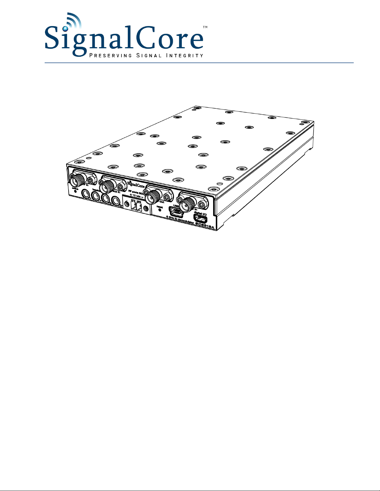
The SC5313A is a core module-based IQ demodulator with all I/O connections and indicators located on
the front face of the module as shown in Figure 1. Each location is discussed in further detail below.
SC5313A Operating & Programming Manual Rev 1.0.2 4
Figure 1. Front view of the SC5313A showing user I/O locations.

Power Connection
LO OUT
This port outputs the tunable LO signal allowing phase-coherent daisychaining of multiple IQ demodulator modules. The connector is SMA female.
The nominal output impedance is 50 Ω.
RF IN
This port accepts an RF signal ranging from 400 MHz to 6 GHz. The connector
is SMA female. The nominal input impedance is 50 Ω. Maximum input power
is +23 dBm with ATTEN #1 set to at least 10 dB attenuation.
RF AUX IN
This port accepts an RF signal ranging from 400 MHz to 6 GHz. This port can
be used as an alternate path for system-level calibration. The connector is
SMA female. The nominal input impedance is 50 Ω.
LO IN
This port accepts a tunable LO signal from an external source to drive the
demodulator. The connector is SMA female. This port is AC-coupled with a
nominal input impedance of 50 Ω. Maximum input power is +10 dBm.
!
!
1
2
Power is provided to the device through a two-position screw terminal block connection as shown in
Figure 1. Proper operation of the device requires +12 VDC source and ground return wires capable of
delivering a minimum current of 1.5 Amps. The polarity of the connector is shown on the front panel of
the RF module, just above the screw terminal block.
RF Signal Connections
All RF signal connections (ports) on the SC5313A are SMA-type. Exercise caution when fastening cables
to the signal connections. Over-tightening any connection can cause permanent damage to the device.
The condition of your system‘s signal connections can significantly affect measurement
accuracy and repeatability. Improperly mated connections or dirty, damaged or worn
connectors can degrade measurement performance. Clean out any loose, dry debris from
connectors with clean, low-pressure air (available in spray cans from office supply stores).
If deeper cleaning is necessary, use lint-free swabs and isopropyl alcohol to gently clean
inside the connector barrel and the external threads. Do not mate connectors until the
alcohol has completely evaporated. Excess liquid alcohol trapped inside the connector may
take several days to fully evaporate and may degrade measurement performance until fully
evaporated.
Tighten all SMA connections to 5 in-lb max (56 N-cm max)
SC5313A Operating & Programming Manual Rev 1.0.2 5
Baseband Connections
Pin Number
USB Function
Description
1
VBUS
Vcc (+5 Volts)
2
D -
Serial data
3
D +
Serial data
4
ID
Not used
5
GND
Device ground (also tied to connector shell)
Pin Number
SPI Function
RS-232 Function
3
MISO
TxD 5 –
RTS
9
MOSI
RxD
11
CS
CTS
15
SRDY
–
17
CLK
CLK
4, 7, 10, 13, 16
GND
GND
2, 8, 12, 14, 18, 19
NC
NC
3
4
The SC5313A has four baseband output ports, comprised of differential in-phase (I+ and I-) and
differential quadrature (Q+ and Q-) outputs. Nominal differential output impedance is 100 Ω. The
demodulator can also be configured for single-ended or differential IF output. When configured for
single-ended operation, it is recommended to terminate the other half of the differential pair using a
50 Ω terminator. All baseband connectors are MCX female.
Communication Connection
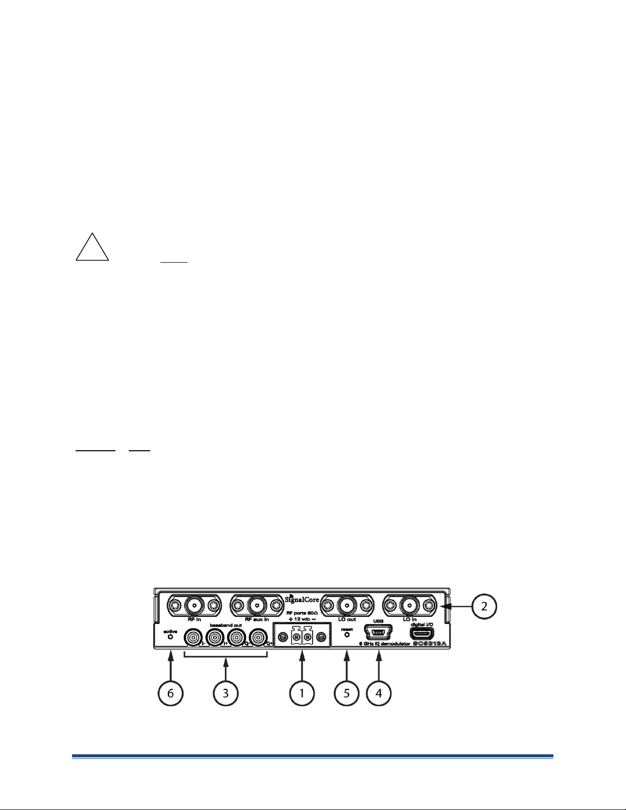
The SC5313A uses a mini-USB Type B connector for primary communication with the device using the
standard USB 2.0 protocol found on most host computers. The pinout of this connector, viewed from
the front of the module, is listed in Table 1.
Table 1. Pinout of the SC5313A USB communication connector.
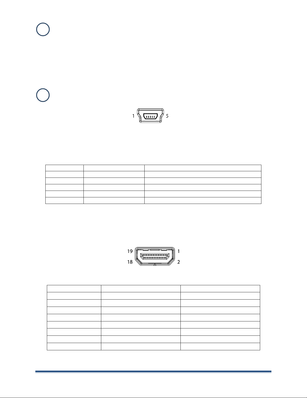
The user can also communicate with the device through the micro-HDMI port. Depending on the
product version ordered, this connector provides either the SPI or RS-232 communication path. The
pinout of this connector, viewed from the front of the module, is listed in Table 2.
Table 2. Pinout of the SC5506A micro-HDMI connector for either SPI or RS-232 communication.
SC5313A Operating & Programming Manual Rev 1.0.2 6
Reset Button
LED
Color
Definition
ACTIVE
Orange
Device is powered on and working properly.
ACTIVE
Green
Device is open (communication has been established). This
indicator is also user programmable. See register map.
ACTIVE
Off
Power fault. Contact SignalCore.
5
6
Depressing this momentary-action push button switch will reset the device to its default state. The
SC5313A has the ability to store the current configuration at any point as the default setting. If the
factory setting has been overwritten with a saved user configuration, resetting the device will reinitialize
the device to the saved user configuration.
Indicator LED
The SC5313A provides visual indication of important modes. There one LED indicator on the unit. Its
behavior under different operating conditions is shown in Table 3.
Table 3. LED indicator states.
SC5313A Operating & Programming Manual Rev 1.0.2 7

S C 5 3 1 3 A T H E O R Y O F O P E R A T I O N
Overview
The SC5313A is a single-stage, direct coversion Inphase-Quadrature (IQ) demodulating mixer, or simply
an IQ demodulator. The SC5313A can operate as a single-stage downconverter or as an IQ demodulator.
The SC5313A demodulator operates in the 400 MHz to 6 GHz RF range with a typical 3 dB IF bandwidth
of 160 MHz in single-stage converter mode, or 320 MHz in IQ mode. The RF input stage has adjustable
gain to allow the user to adjust the incoming RF signal prior to the demodulation process for the
purpose of optimizing RF dynamic range. The IF stage has adjustable gain to ensure that linearity and
noise of the IF output are optimized. The SC5313A has the necessary RF amplifiers, attenuators, IF
amplifiers, and IF control via DACs to allow the user to optimally operate the device over the entire
frequency range as well as for both small and large RF input levels. Figure 2 shows a simplified block
diagram of the SC5313A, showing only the signal conditioning components critical for the following
discussion. The following sections below provide more in-depth discussion on how to optimize the
converter for linearity and signal-noise dynamic range. Power supply generation and regulation, and
digital control functions are not covered. Should the user require more information than what is
provided in this manual, please contact SignalCore.
RF Input Section
In the design of the RF input section, care was taken to ensure that the dynamic range of the IQ
demodulator is preserved as seen at the input port of the device. This requires that the demodulator is
not driven too hard (high signal amplitude) nor too soft (low signal amplitude). When the device is
driven hard, nonlinear effects dominate the system. When driven too softly, signal-to-noise dynamic
range suffers. A general rule is to apply more attenuation earlier in the RF signal path to improve
linearity, and more gain to improve signal-to-noise performance. As an example, for a given input signal
level and while maintaining a relatively constant output IF level, the user would switch in RF AMP#1 and
apply attenuation on ATTEN#3 to improve signal-to-noise dynamic range. The factory default state sets
all the RF amplifiers off, all attenuators set to 0 dB attenuation, and the IF gain set to 8 dB (DAC code of
32). In this default state, the device is optimized for a -10 dBm RF signal in the 1.0 GHz to 2.4 GHz range.
The IF output is typically 0.5 V – 1.0 V peak-to-peak differential at these settings.
The RF amplifiers are used to improve the gain of the device if the input signal is too low or when the
losses at higher frequencies are large. RF AMP#1 is usually selected when the RF signals are lower than
-25 dBm at the input port. With RF AMP#1 enabled, the device sensitivity is improved and the detection
of low level signals is better resolved. RF AMP#2 should be selected and switched into the signal path at
RF frequencies greater than 5 GHz, where the signal power loss through the front end prior to the
demodulator can be as high as 15 dB due to filter and switch insertion losses. At these high RF
frequencies, if the IF gain is at its maximum of 15.75 dB (DAC code = 63) and the IF output level falls
below -10 dBm or outside the digitizers optimal levels, RF AMP#2 should be enabled.
SC5313A Operating & Programming Manual Rev 1.0.2 8
 Loading...