

Page 1
Integrated Mixed-Signal Solutions
PRODUCT DATA SHEET
STMP35xx
D-Major™Audio System on Chip
with USB 2.0, LCD, Voice Record and Battery Charger
Third Generation Audio Decoder
Version 1.06 July 16, 2004
Host Processor
(Optional)
Rechargeable
Battery
LED/LCD Screen
FM Tuner
9
0
9
4
9
8
1
0
2
1
0
6
Hi-Speed USB
Microphone
Voice Record
OFFICIAL PRODUCT DOCUMENTATION 8/10/04
5-35xx-D1-1.06-071604
Flash Memory
Hard Drive
Buttons/Switches
SDRAM
Headphones
CD Pickup
Copyright © 2004 SigmaTel, Inc.
All rights reserved.
SigmaTel, Inc. makes no warranty fo r t he use of i ts pr od uc ts, a ssu mes no res po nsi bil ity fo r a ny err or s wh ich may app ea r in t his document,
and makes no commitment to update the information contained herein. SigmaTel reserves the right to change or discontinue this product at
any time, without notice. There are no express or implied licenses granted hereunder to design or fabricate any integrated circuits based on
information in this document.
The following are trademarks of SigmaTel, Inc., and may be used to identify SigmaTel products only: SigmaTel, the SigmaTel Logo, C Major,
D Major and Go-Chip. Other products and company names contained herein may be trademarks of their respective owners.
Page 2

OFFICIAL PRODUCT DOCUMENTATION 8/10/04
STMP35xx
D-Major™Audio System on Chip
1. TABLE OF CONTENTS
1. TABLE OF CONTENTS .....................................................................................................................2
2. PRODUCT OVERVIEW .....................................................................................................................3
3. CHARACTERISTICS/SPECIFICATIONS ........................................................................................ 21
4. DSP CORE .......................................................................................................................................25
5. ON-CHIP MEMORY SUBSYSTEM ..................................................................................................30
6. CHIP WIDE PROGRAMMABLE CONTROL REGISTERS .............................................................38
7. INTERRUPT SUBSYSTEM ..............................................................................................................49
8. USB CONTROLLER ........................................................................................................................60
9. INTEGRATED USB 2.0 PHY (HS,FS) .............................................................................................79
10. PARALLEL EXTERNAL MEMORY CONTROLLER (EMC) .......................................................103
11. GENERAL PURPOSE FLASH CONTROLLER ..........................................................................118
12. FLASH ECC ACCELERATOR ....................................................................................................134
13. FILTER COPROCESSOR (FILCO) .............................................................................................154
14. PULSE WIDTH MODULATOR (PWM) CONTROLLER .............................................................. 185
2
C INTERFACE ...........................................................................................................................196
15. I
16. ENHANCED SPI INTERFACE .....................................................................................................209
17. SPI INTERFACE ..........................................................................................................................217
18. TIMERS ........................................................................................................................................220
19. SDRAM INTERFACE ...................................................................................................................227
20. SWIZZLE ..................................................................................................................................... 239
21. REAL-TIME CLOCK/ALARM/WATCHDOG RESET & PERSISTENT BITS .............................. 248
2
S SERIAL AUDIO INTERFACE ................................................................................................259
22. I
23. GENERAL PURPOSE INPUT/OUTPUT (GPIO) .........................................................................266
24. DAC ..............................................................................................................................................276
25. ADC ..............................................................................................................................................286
26. MIXER ..........................................................................................................................................297
27. HEADPHONE DRIVER ................................................................................................................310
28. LOW RESOLUTION ADC ............................................................................................................315
29. BOOT MODES .............................................................................................................................329
30. DC-DC CONVERTER ..................................................................................................................339
31. PIN DESCRIPTION .....................................................................................................................377
32. PACKAGE DRAWINGS ...............................................................................................................389
33. STMP35XX FAMILY MEMBER PART NUMBERS & ORDERING INFORMATION ...................391
34. INDEX OF REGISTERS ...............................................................................................................393
ADDITIONAL SUPPORT
Additional product and company information can be obt ained by goin g to the SigmaTel website at:www.sigmatel.com
available for authorized customers at: extranet.
2 5-35xx-D1-1.06-071604
. Additional product and design information is
sigmatel.com
Page 3

OFFICIAL PRODUCT DOCUMENTATION 8/10/04
STMP35xx
D-Major™Audio System on Chip
2. PRODUCT OVERVIEW
2.1. Features
• Decodes MP3 and WMA and is upgradeable to other digital music formats
• Supports WMA Digital Rights Management (DRM) and other security schemes
• Includes on-chip read only unique ID for digital rights management algorithms
• USB High Speed Device Interface (up to 480Mb/s transfers)
• Enables file transfer and firmware upgrade using USB Mass Storage Class
• Both Windows and Macintosh drivers available
• Integrated USB High S peed PHY
• Direct connection to USB 5V power for operation and battery charging
• 96K Words (288K Bytes) of on-chip RAM
• Hardware support for flexible external storage options
• NAND Flash, MMC, Secure Digital, SmartMedia, CompactFlash
• Five byte address support for new 1Gb/die (128KB block) NAND Flash
• MLC NAND Flash support
• 1.8V NAND Interface Support
• 16 bit wide NAND support
• Hardware
• SDRAM
• ATA/IDE Hard Disk digital devices.
• Optimized for very long battery life
• 50 hours of operation on a single AA battery
• Flexible, efficient on-chip DC-DC converter
• Flexible battery configurations, including 1xAA, 1xAAA, 2xAA, 2xAAA, LiIon
• Pulse frequency modulation mode for low standby power
• Energy saving dynamic power management
• Typical off current is 250µ
• More than 1 year battery life in “off” mode on one AA Alkaline battery
• Integrated battery charger for LiIon and NiMH
• Battery temperature sensor support for safest charging protocols
• Real time clock with alarm function wakes up from powerdown/standby modes
• High quality integrated audio mixed signal sub-system
• <0.05% THD direct drive headphone amplifier
– Eliminates DC blocking capacitors
– Including anti-pop and short-circuit protection
• High performance 18-bit Σ∆ technology stereo D/A and A/D converters
• Full analog mixer configuration
• Line-in to Headphone/Line-out SNR >90 dB
• Two an alog line-level input s: Line1 In (stereo), Line2 In ( stereo, 144-pin p ackage)
• Mic(mono) input with integrated pre-amp and microphone biasing circuit
• Volume control
• GPIO, button I/O controls, and LCD/LED Disp lay Compatible Inter face
• Pulse Width Modulators for EL backlights
• Integrated 75MHz DSP with Filter Coprocessor for power optimization
• Optimized for audio applications
• Field upgradeable firmware
accelerated ECC off-loads DSP bit error correction
A (crystal oscillator & real time clock only)
5-35xx-D1-1.06-071604 3
Page 4
OFFICIAL PRODUCT DOCUMENTATION 8/10/04
STMP35xx
D-Major™Audio System on Chip
• Integrated Development Environment, SDK, and debugger
• Application and support libraries
• Bass and Treble control; configurable multiple band EQ control
• Voice record in ADPCM format (upgradable to other formats)
• FM tuner input and control support
• Optional interface to a host chip/processor for cell phone & PDA applications, etc.
• Application notes, reference schematics, sample PCB layouts are available.
• Offered in 100-pin TQFP, and 144-pin fpBGA packages
• Backward pin and firmware compatible with STM P3 4 10
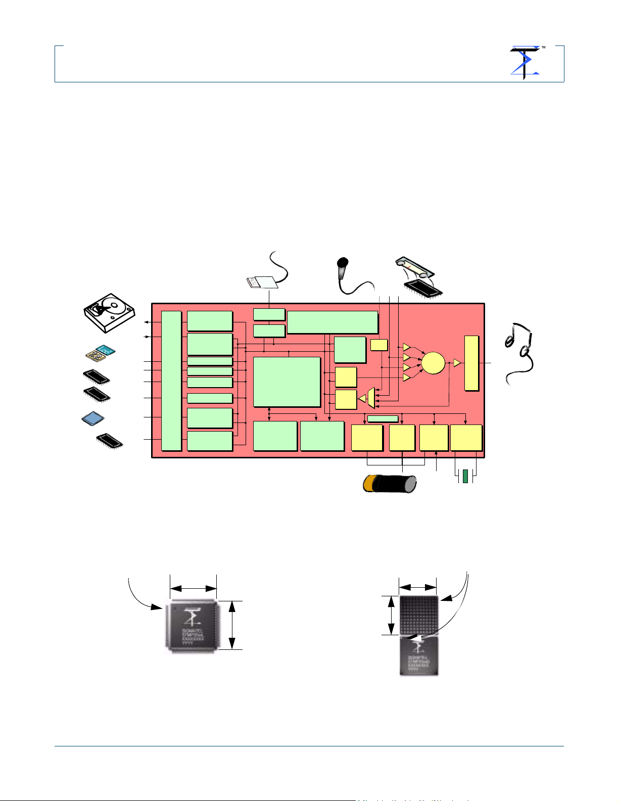
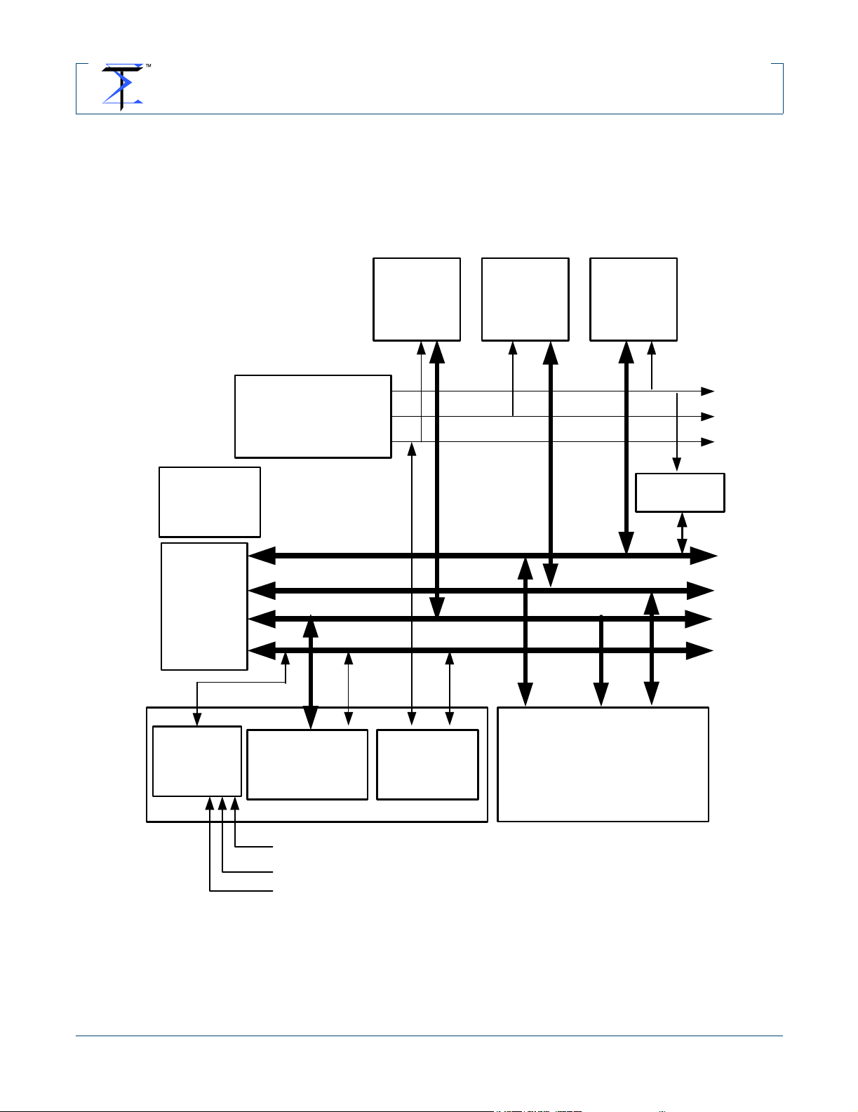
2.2. STMP35xx Block Diagram
9
0
9
4
9
8
1
0
2
1
0
6
Hard Drive
LED/LCD
Buttons/
Switches
E.L. Backlight
MMC/SD
Card
I2C
Peripherals
SmartMedia
CompactFlash
NOR Fla sh
NAND Flash
MLC Flash
SDRAM
Pin 1
Synchronization
Synchronization
GPIO Interface
I/O Pin Multiplexer
General Purpose Input/Output
14 mm
CD Control
IDE Interface
Interface
I2 S & CD
I2S CD
Interface
I2C Interface
Pulse Width
SPI Interface
SPI Interface
SPI Interface
I2C Interface
I2C Interface
Flash/IDE
EMC
Interface
SDRAM
SDRAM
Interface
Interface
USB High Speed
USB Full Speed
USB PHY
USB
(HS & FS)
USB 2. 0
USB
Device
24-bit
DSP
On-Chip ROM
On-Chip ROM
16K x 24bits
8K x 24bits
Inte rrupt Control, Timers,
Interrupt Control, Timers, Bit
Bit Manipulation Unit,
Manipulation Unit, RTC, Trace
Trace Debug Unit
Debug Unit, Reed-Solomon
Memory Bus
Peri p he ral Bus
DSP
On-Chip RAM
On-Chi p RAM
96K x 24bits
96K x 24bits
Microphone
Filter &
ECC
USB
engines
DAC
DAC
ADC
ADC
Low
DCDC
Resolution
Converter
ADC x3
Rechargable Battery
Figure 1. Chip Block Diagram
FM Radio
Mic in
Amp
DAC
Temperature
FM in
Low
Battery
Resoluti
Charger
on ADC
10 mm
STMP35xx
Line in
Σ
Σ
DCDC
DCDC
Converter
Converter
Input
5V
Headphone Amplifier
RTC,
ALARM,
PLL
PLL,
xtal
XTAL
Crystal
Pin A1
Headphone Amplifier
Headphones
Cap-less
Direct Drive
10 mm
14 mm
100-pin TQFP
For additional package measurements, please see 32. “PACKAGE DRAWINGS” on page 389.
Figure 2. Chip Package Photos
4 5-35xx-D1-1.06-071604
144-pin fpBGA
Page 5

OFFICIAL PRODUCT DOCUMENTATION 8/10/04
STMP35xx
D-Major™Audio System on Chip
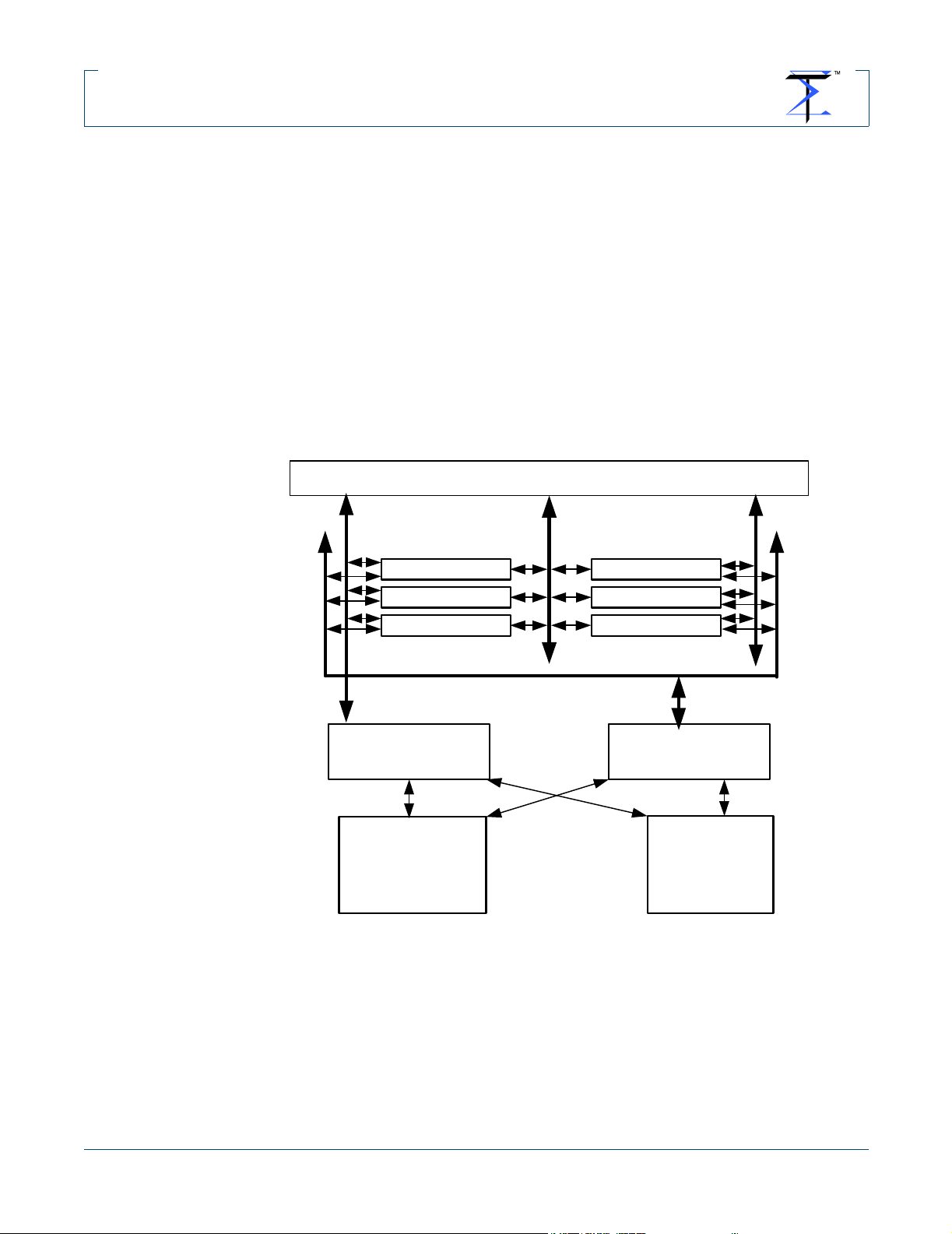
2.3. Description
SigmaTel's STMP35xx is a third generation single-chip highly-integrated digital music
system solution for devices such as digital audio players, PDAs, voice recorders, MP3encode recorders, and cell phones. It includes a high performance DSP, 288KBytes of
on-chip SRAM, and a USB 2.0 interface (including High speed 480Mb/second transfers)
for downloading music and uploading voice and MP3 recordings. The chip also includes
a mixer, DAC, ADC and provides interfaces to IDE Hard Drives, CD-DSPs, Flash memory, LCD/LEDs, button & switch inputs, headphone driver, FM tuner input & controls and
a microphone. The chip’s highly programmable architecture supports MP3, WMA, and
other digital audio standards. WMA digital rights management and other security
schemes are also supported. For devices like PDAs and cell phones, the STMP35xx
can act as a slave chip to a host chip/processor.
The DAC includes a headphone driver to directly drive low impedance headphones. The
ADC includes inputs for both microphone and analog audio in to support voice recording &
FM radio integration and MP3 encode features. Si gmaTel's propr ietary Sig ma-De lta ( Σ∆)
technology achieves a DAC SNR in excess of 90 dB for high-quality audio playback.
The STMP35xx has low power consumption to allow long battery life and includes an
efficient flexible on-chip DC-DC converter that allows many different battery configurations, including 1xAA, 1xAAA, 2xAA, 2xAAA and LiIon. Th e chip inclu des a n inte grat ed
intelligent charger for NiMH and LiIon batteries. In addition, the single-chip design and
low pin count enables very small digital audio devices to be designed.
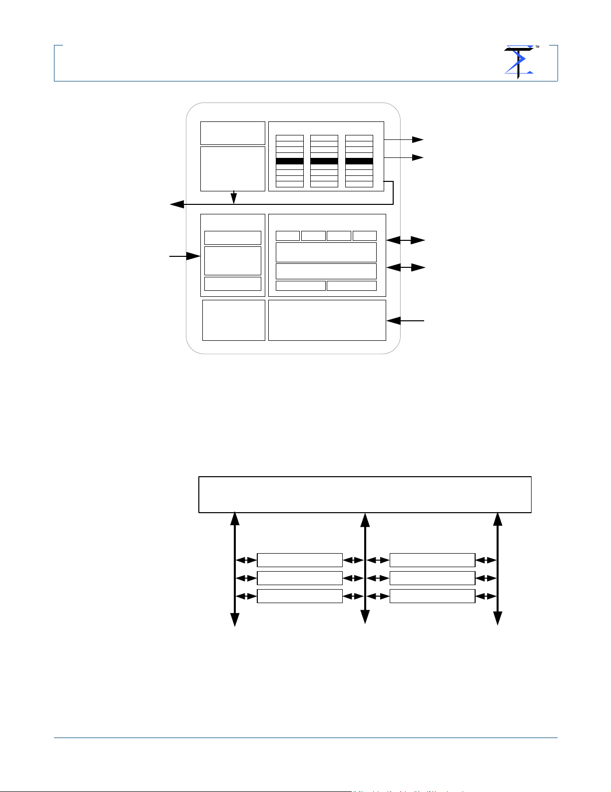
2.3.1. DSP Core
The on-chip DSP core is modeled exactly after the Motorola DSP56004. It supports
the identical instruction set, registers, addressing modes, etc., as the DSP56000
family of digital signal processors. Figure 3 shows a high level view of the DSP core.
This architecture is highly optimized for battery operated audio applications. Its 24bit intrinsic data size provides sufficient precision for high quality audio algorithms
while minimizing the number of register and data path signals that must be toggled
for any operation. The term “WORD”, as used in this data sheet, refers to a 24-bit
unit of storage unless otherwise noted.
The functionality that defines the on-chip DSP, is the memory map, interrupt processing, and peripherals it offers.
The integrated DSP comprises three execution units, an interrupt controller and a
debug interface. It connects to the rest of the STMP35xx chip via thr ee memory busses, a set of interrupt input signals and various reset and clock inputs. It implements
a 3 memory space Harvard architecture, simultaneously referencing an X data element, a Y data element and a program element. These references are conveyed
over the program or “P” bus, the X b us and the Y bus. Ea ch bus c omprises a 24 bit
wide data path and a 16 bit address bus. Program accessible I/O registers reside in
the top 4K word addresses on the X-bus. The DSP architecture has special programmed I/O support for the to p 64 words of this space bu t Sigm aTel has extended
this space to the top 4K words, i.e. addresses $F000 through $FFFF, inclusive.
The DSP Core also implements the OnCE debugger that is the norm for this DSP
architecture. The OnCE interface connects to an external debugger over four I/O
signal pins on the STMP35xx.
Using an industry standard instruction set architecture and debugger interface for
the integrated DSP means that development tools and debuggers are in the highly
evolved and stable portion of their life cycle. In addition, it means that system devel-
5-35xx-D1-1.06-071604 5
Page 6
OFFICIAL PRODUCT DOCUMENTATION 8/10/04
STMP35xx
D-Major™Audio System on Chip
DSP Core
Address to
X space
Address to
Y space
Data to/from
X space
Data to/from
Y space
Interrupts
To/from
P space
Debug Interface
Program
Address
Generator
ProgramDecoder
Instruction Latch
Decoder
&
State Machines
Registered Control
Bit Manipulation
Unit
Address
R0
R1
R2
R3
R4
R5
R6
R7
DATA ALU
X0 X1
A
Generation Unit
N0
N1
N2
N3
N4
N5
N6
N7
M0
M1
M2
M3
M4
M5
M6
M7
Y0 Y1
x
+
B
Interrupt
Controller
Figure 3. DSP Core at a Glance
opers with experience developing on this DSP can be found. The Sigma Tel sof twar e
developers kit (SDK) provides an excellent integrated development environment
with an assembler, C compiler, debugger and other re quisite tools.
2.3.2. On-chip RAM and ROM
The STMP35xx includes 96K words of on-chip RAM. This amounts to 2.25Mbits of
on-chip SRAM in six 16K Word blocks. The RAM is split into two 48K word banks
with one bank attached to the X bus and one attached to the Y bus. The P bus is
X-BUS
16KW or d S RAM
16KW or d S RAM
16KW or d S RAM
Figure 4. 6 x 16K Word On-chip SRAM Blocks
connected to both RAM banks so that program space can be allocated from the
same two banks that hold X and Y data values. An adjustable switching mechanism
DSP CORE
P-BUS
Y-BUS
16KWord SRAM
16KWord SRAM
16KWord SRAM
6 5-35xx-D1-1.06-071604
Page 7
OFFICIAL PRODUCT DOCUMENTATION 8/10/04
STMP35xx
D-Major™Audio System on Chip
is provided so that a portion of the X bus RAM or Y bus RAM can be allocated to the
P bus in units of 8K words from 0K to the full 64K words.
A typical application will allocate a portion of the X bus RAM and another portion of
the Y bus RAM to the P bus. In normal operation, this switching mechanism will
present a contiguous block of RAM beginning at location zero in the P bus address
space, or P:$0000 as it is written in assembler syntax
Suppose we allocate 24K Words from the X bus RAM to the P bus and another 24K
Words from the Y bus RAM to the P Bus. This gives us 24K Words of X RAM, 24K
Words of Y RAM and 48K Words of P RAM fo r o ur ap plication . All 96K Words of onchip SRAM are allocated, as shown in Figure 5.
$FFFF
$F000
$6000
$5FFF
X
Address
Space
PIO
Regs.
No
SRAM
24K
Words
X
RAM
$BFFF
48K Words Physical SRAM
$C000
P
Address
Space
on-chip
ROM
24K
Words
from
Y
RAM
24K
Words
from
X
RAM
$BFFF
48K Words Physical SRAM
Y
Address
Space
No
SRAM
$5FFF
24K
Words
Y
RAM
$0000
Figure 5. On-Chip RAM Allocation Example
The STMP35xx contains an on-chip 16K Word ROM which holds the Bootstrap
code. At power-on time, the first instruction executed by the DSP comes from this
ROM. Power-on reset causes the on-chip ROM to be placed at P:$0000. The reset
interrupt vector is located at P:$0000, thus the first instructions executed come from
this ROM. Software in this ROM offers a large number of BOOT configuration
options, including manufacturing boot modes for “burn-in” and “tester” operation.
Other boot modes are responsible for loading app lication code from off-chip into the
on-chip RAM. Off chip sources for application bootstrapping include:
• External NAND FLASH
• Host (PC) controlled bootstrapping using USB,
5-35xx-D1-1.06-071604 7
Page 8
OFFICIAL PRODUCT DOCUMENTATION 8/10/04
STMP35xx
D-Major™Audio System on Chip
• Host (PC) controlled bootstrapping using I2C slave.
2
•I
C Master transfers from serial EEPROM
Once the on-chip boot code has loaded the application code into on-chip RAM, it
can relocate the 16K Word on-chip ROM to the very top of the P address sp ace, se e
Figure 5. “On-Chip RAM Allocation Example” on page 7. The on-chip ROM can be
disabled entirely so that all 64K words of P space is available for on-chip RAM.
The on-chip boot code includes a firmware recovery mod e. If the de vice fails to bo ot
from NAND flash, for example, the device will boot from a PC host connected to its
USB port. This firmware recovery m ode can be invoked at anytime by holding the
PSWITCH or “play” button for at least five seconds during power up.
The on-chip RAM serves as one end of all DMA transfers, e.g either the source or
destination. Every SRAM block has three potential accessors: P-BUS, DMA-BUS,
and its respective X-BUS or Y-BUS. A number of the integrated peripheral controllers use a distributed DMA implementation to transfer data to or from on-chip
SRAM.
DSP CORE
X-BUS
16KWord SRAM
16KWord SRAM
16KWord SRAM
DMA-BUS
Exter nal Flash/I DE
External SDRAM
USB
FLASH ECC
Figure 6. On-Chip RAM & Distributed DMA
In this distributed DMA architecture, all of the peripheral controllers that use DMA
share a common DMA address and data bus path to and from on-chip RAM. Each
peripheral controller implements its own a ddress ge nerator. Address generation can
be highly sequential as in the case of the D/A converter or fairly random as in the
case of the USB controller. Thus each device that uses the distributed DMA will
have at least one base address register (HW_xxxBAR) and various address modifying registers. Most of the distributed DMA devices implement some form of circular
buffering in their addressing modes. There is a centralized arbiter that selects wh ich
of the distributed DMA peripheral co ntrollers has access to the DMA bus on any
given clock cycle.
P-BUS
Y-BUS
16KWord SRAM
16KWord SRAM
16KWord SRAM
CD
D/A
A/D
Trace Buffer
Filter Coproc.
8 5-35xx-D1-1.06-071604
Page 9

OFFICIAL PRODUCT DOCUMENTATION 8/10/04
STMP35xx
D-Major™Audio System on Chip
With a DSP core clock of 65MHz, a single block of on-chip RAM can provide 65MHz
times 3 bytes or 195 MByte/second of bandwidth. There are four 24 bit data busses
connected to the on-chip SRAM blocks. Furthermore, each SRAM block is single
ported and has its own independent address and data busses. Thanks to the arbitration logic in this memory subsystem, all four busses (P, X, Y, DMA) can be made
to cycle on every clock. Thus the peak bandwidth available from the on-chip RAM is
four times 195 MByte/second or 780 MByte/second.
Of course, there are times when more than one data bus needs to transfer into or
out of the same SRAM block. When conflicts occur, the arbiter will “stall” the DSP for
one (or more) clock(s) to resolve the conflict.
The reader should not be surprised to see devices like A/D or D/A converters using
DMA transfers. Some readers may be surprised to learn that external FLASH and
external SDRAM are only accessible via the DMA. Th e external memories are not
mapped into the “load/store” space of the DSP’s instruction set.
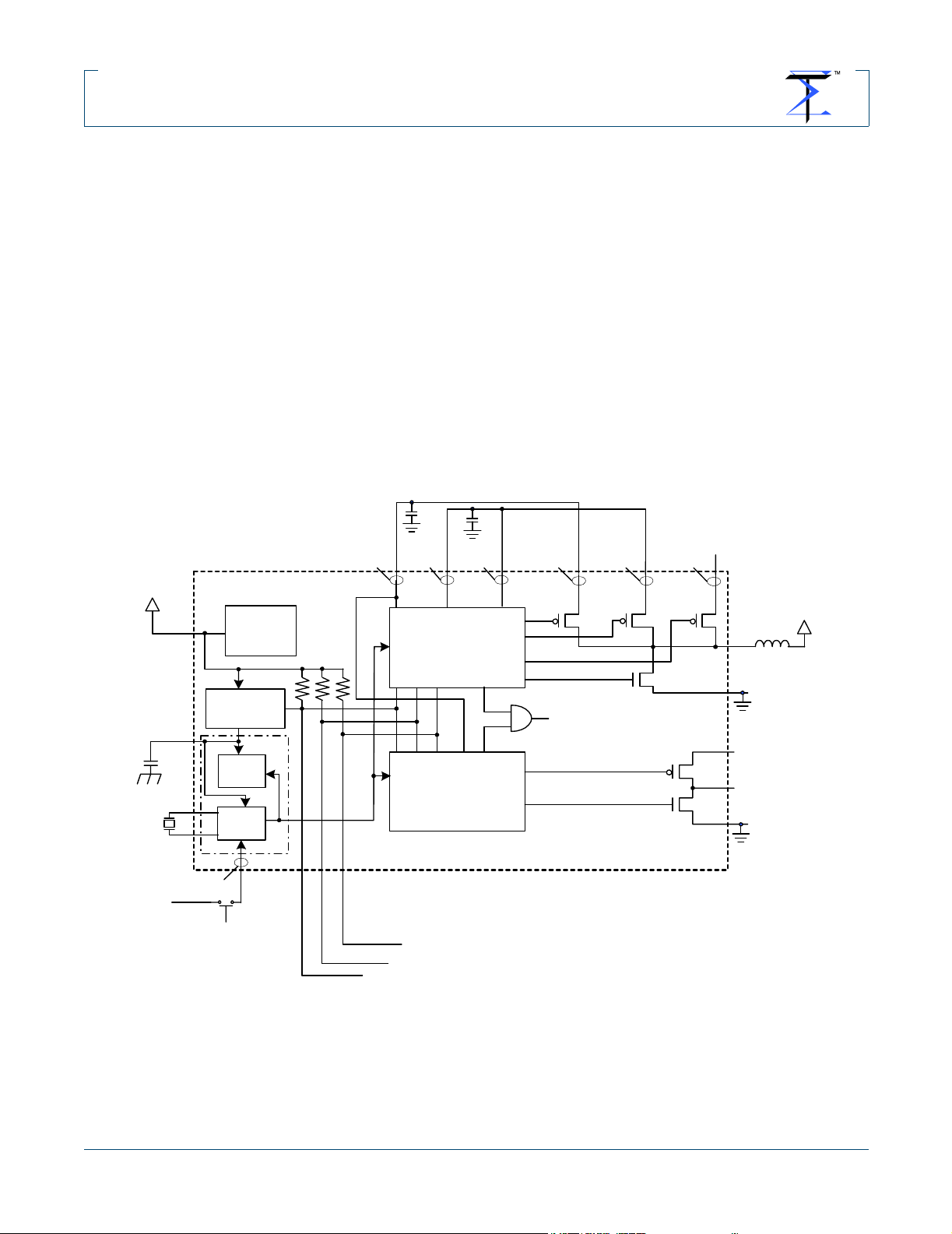
2.3.3. Power Subsystem
The STMP35xx contains a sophisticated pow er subsystem inc luding two inte grated
DC to DC converters to produce a very cost effective product with flexible battery
configurations. In addition, it contains power monitoring circuits for battery brownout
detection as well as system overload br ownout detection. The chip also contains
detection circuits for battery installation and removal. It manages power state
changes caused by battery changes or from monitoring the on/off power switch circuit.
The chip has two programmable integrated DC-DC converters that can be used to
provide power for the device as well as the entire application. The converters can be
configured to operate from standard battery chemistries in the range of 0.9-4.2 volts
including alkaline cells, NiMH, LiIon etc. These converters use off chip reactive components (L/C) in a pulse width or frequency modulated DC to DC converter.
The DC to DC converter circuit consists of the of f-ch ip reactive component s, an integrated controller and integrated low resistance FET switches. The DC-DC converter
#1, as shown in Figure 7, has one n-channel FET and three independently controlled p-channel FETs generating three independent channels of separately controlled voltages. For the case shown, the battery is a sin gle AA alkaline battery in the
range 0.9 to 1.5 volts. DC-DC converter # 1 is used to “boost” this input voltage to
3.3 volts for use in driving the I/O VDD rail and two separate 1.8 volt sour ces for
driving the analog VDD rail and the digital VDD rail. This case is shown in the first
row of Table 1, “Flexible Battery Config urations,” on page 11. Other rows show different configurations supported by the DC to DC converters. For example, when th e
battery chemistry provides an input voltage that is higher than that desired for the
I/O rail, digital rail or analog rail, then the DC to DC converte rs can opera te in “buck”
mode which provides a regulated output that is lower than its input.
One obvious use for the DCDC converter is in boosting the output of a nearly
depleted alkaline battery delivering 0.9 volts up to th e re gula te d 3. 3 vo lt I/O rail voltage and the regulated 1.8 volt digital and core rails. The DCDC converter can also
be used to lower the voltage of a 4.2 v olt LiIon b attery down to the 1.8V digital core
and analog rails. Table 1, “Flexible Battery Configurations,” on page 11 shows various battery configurations that can be sup po rt ed .
1
1.Note VddA3 == VddHP, VddA4== VddPLL. The analog power pair formerly known, in the STMP3410,
as VddA2 and VssA2 have been redefined for the STMP35xx as Vdd5V and LRADC2.
5-35xx-D1-1.06-071604 9
Page 10
OFFICIAL PRODUCT DOCUMENTATION 8/10/04
STMP35xx
D-Major™Audio System on Chip
In addition, the DCDC converter can regulate these voltages to lower the standard
core and I/O values to extend the battery life. Recall that energy consumed in a
CMOS AC circuit is proportional to V
These program controlled reductions in operating voltage are used in various SigmaTel software applications to provide very long battery life products. The
STMP35xx also contains a silicon speed sensor so that each device can tailor its
operating voltage to the minimum required for safe operation as constrained by its
individual silicon process parameters and junction temperature.
The DC to DC converters control the power up sequence of the device and hold the
rest of the chip in reset until the power supplies have stabilized at the correct voltages. The power up sequence begins when the battery is connected to the BATT
pin. As shown in Figure 7, the crystal oscillator will begin running as soon as the battery is connected and the pswitch is asserted. The crystal oscillator and the real
time clock (RTC) can be programmed to continue to operate even when the player
is in the off state. The crystal oscillator and RTC are the only drains on the battery in
the off state and designed for very small energy consumption. The RTC module
includes an alarm function that can be used to “wake-up” the DC to DC converters
which will then wake up the rest of the system.
2
so this reduction can be quite significant.
battery
BATT
VddXTAL
Resolution
Regulator
VddXTAL=BATT
RTC
XTAL
OSC
Pswitch
Power Button
VddA
1/2/3
DC-DC
(boost mode)
DC-DC
* only available on 144-pin package
DCDC_VddIO
Low
ADC
VddIO
1/2/3*/4*
DCDC_mod2
DCDC_mod0*
DCDC_mod1*
VddD
1/2/3
#1 Control System
#2 Control System
NC
NC
NC
Figure 7. Lowest Cost 1xAA 100-pin Configuration
DCDC_VddD
DSP_RESET
medium V (2 Alkaline/NimH)
or hi V LiIon Applications
DCDC_VddA*
1
NC
battery
DCDC_Batt
DCDC_Gnd
NC
DCDC2_Vout*
NC
DCDC2_Batt*
DCDC2_Gnd*
The power down sequence is also controlled by the DC to DC converters. When a
power down event is detected, they return the player to the power off state. In the
power off state with non-LiIon chemistries, the I/O Vdd rail is connected to the Battery and the internal VddD and VddA rails are pulled down to ground to minimize
10 5-35xx-D1-1.06-071604
Page 11

OFFICIAL PRODUCT DOCUMENTATION 8/10/04
STMP35xx
D-Major™Audio System on Chip
leakage currents. For LiIon mode, the I/O Vdd rail is connected to ground instead of
connecting to BATT.
In addition to the various voltage detectors, a power up or p ower down eve nt can be
signaled by the special power switch circuitry in the DC to DC converters. A simple
resistor network and momentary contact push button switch is sufficient for player
on/off control.
There is a special three channel low resolution A/D converter on-chip to help with
battery based applications. One channel is dedicated to measuring the voltage on
the BATT pin and is used to monitor the battery condition to estimate its remaining
life. All low resolution channel also have digital trip point comparator functions that
can be used to generate inter rupts to the DSP. The trip point can be program matically set at one of 512 levels for battery b rown out detect ion on the Battery LRADC
or for threshold detection on the other two LRADCs. NOTE: ONLY the battery can
be connected directly to the BATT pin for correct operation of the device, thus the
battery channel of the low resolution A/D converter is not available for any other purpose. The second and third low resolution A/D converters are uncommitted and
available for application use. An optional current source can be enabled to either the
second or third LRADC pin to support external temperature sensors with minimal
external components.
In addition, the DC to DC converters have comparators to monitor their output voltages. They can report “brownout” conditions resulting from over dr awing their power
capabilities. These conditions are reported either on a normal interrupt level or as a
non-maskable interrupt (NMI).
The device contains an integrated PLL which is referenced to the 24.0MHz crystal
oscillator. It can generate clock sources from 39.6MHz to 120.0MHz in steps of
1.2MHz. It includes a post divide stage for the dig ital cloc k fro m a div ide by one to a
divide by 2048. With the PLL turned off and the post divider set to 2048, one can
achieve a low power 11.7KHz operating point.
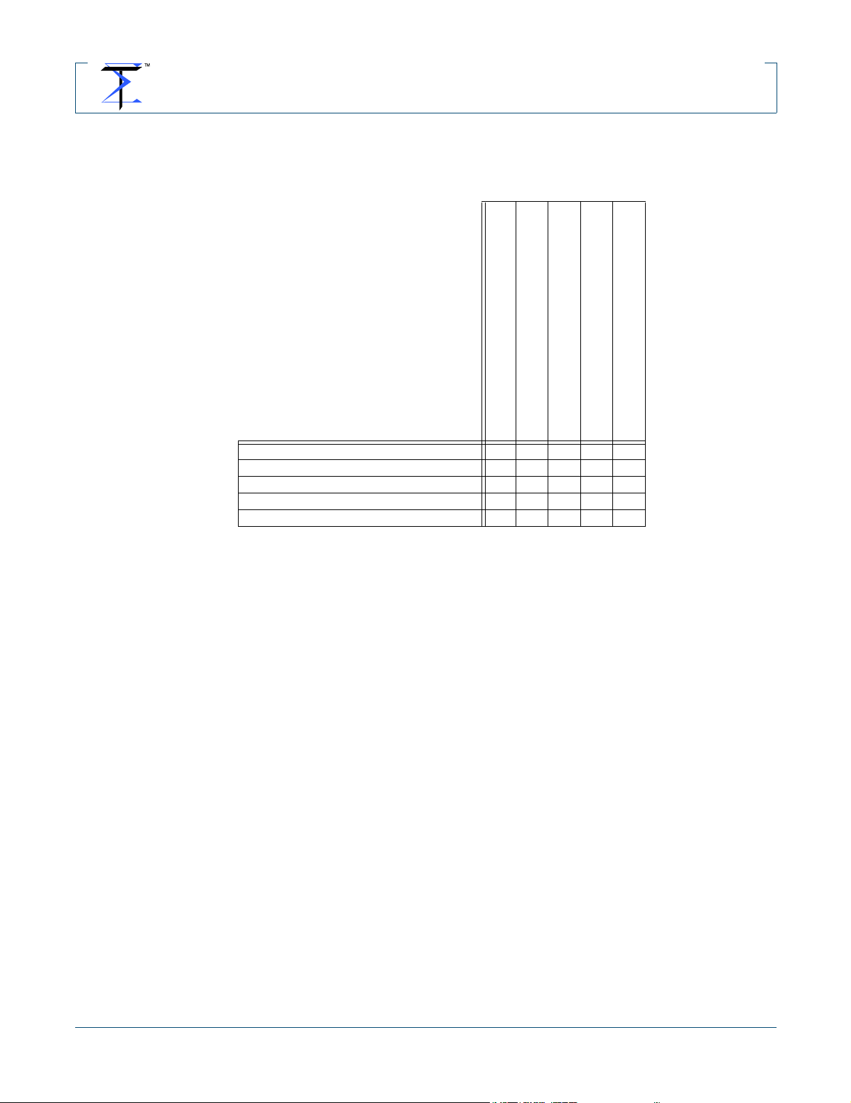
POWER SOURCE VDD I/O VDD D VDD A
1 Alkaline or 1 NiMH
(0.9V-1.5V)
1 Alkaline or 1 NiMH
(0.9V-1.5V)
LiIon, (3.0-3.6V) LiIon Battery DCDC1
2 Alkaline or 2 NiMH
(1.8V-3.0V)
LiIon (3.3V-4.2V) DCDC2
DCDC1
DCDC_VddIO
Boost
3.3V
DCDC1
DCDC_VddIO
Boost
3.3V
DCDC2
Boost
3.3V
Buck
3.3V
Table 1. Flexible Battery Configurations
DCDC1
DCDC_VddD
Boost
1.8V
DCDC1
DCDC_VddD
Boost
1.8V
lowest cost (shared
passives & 100-pin)
Buck
1.8V
DCDC1
Buck
1.8v
DCDC1
Buck
1.8V
DCDC1
DCDC_VddA
Boost
1.8V
better noise floor
(144-pin)
DCDC1
DCDC_VddD
Boost
1.8V
DCDC1
Buck
1.8V
DCDC1
Buck
1.8V
DCDC1
Buck
1.8V
5-35xx-D1-1.06-071604 11
Page 12
OFFICIAL PRODUCT DOCUMENTATION 8/10/04
STMP35xx
D-Major™Audio System on Chip
There is an integrated watchdog reset timer available for automatic recovery from
catastrophic software errors. If programmed by software, this circuit will generate a
reset sequence if its timer is ever allowed to reach zero. Normally functio ning s oftware will reload the watchdog count before expiration of the count. The maximum
delay until a watchdog reset is greater than four hours.
2.3.4. Battery Charger
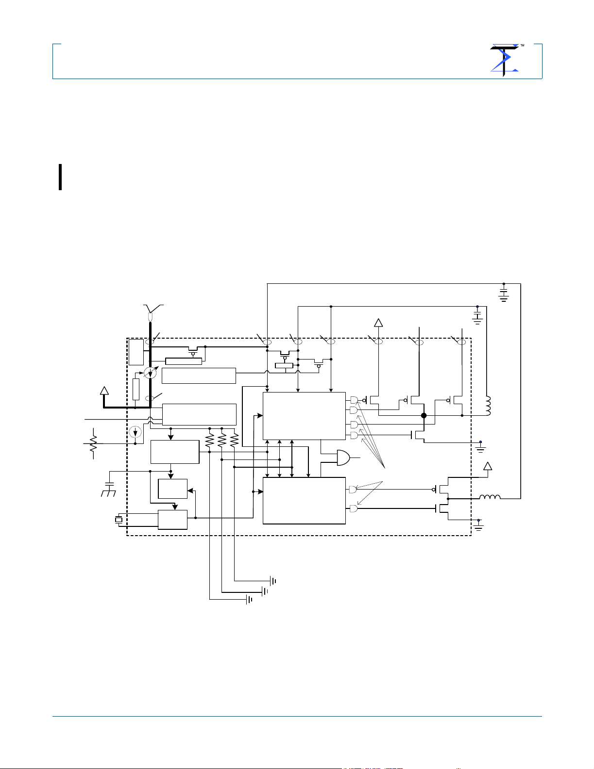
The STMP35xx integrates support for LiIon charging protocols in USB or AC line
attached environments. When the 5 V source is detected on the VDD5V pin the
power management system autom atically reconfigures to use the integr ated linear
regulators to supply the core and I/O rails. Software can then enable the integrated
current source to provide battery charge current, as shown by the bold path in Figure 8. The variable current sources tappers of the charge current as it approaches
the maximum LiIon battery voltage. Software can then take over to control the final
“topping-off” algorithm, as desired.
USB Vbus 5v Line 5V input
>4.35V
VDD5V
5V
detect
Linear Reg.
battery
Charge Current Path
BATT
LRADC1
LRADC2
Temp.
VddXTAL
V Sense
Low Resolution AD C
Regulator
VddXTAL=BATT
RTC
XTAL
OSC
linear charger
controller
3 Channel
DCDC_mod2
DCDC_mod1*
VddIO
1/2/3*/4*
DCDC_mod0*
VddD
1/2/3
Linear
#1 Control System
#2 Control System
VddA
1/2/3
DCDC_VddIO
DC-DC
(boost mode)
DC-DC
* only available on 14 4-pi n p ac kages
battery
DCDC_VddD
DSP_RESET
disabled during linear
battery charge
NC
DCDC_VddA*
NC
DCDC_Batt
DCDC_Gnd
DCDC2_Vout*
DCDC2_Batt*
DCDC 2_G nd*
MODE = 000, for LiIon, both converters in buck mode
battery
Figure 8. Integrated LiIon Battery Charger
2.3.5. USB Interface
The chip includes a Universal Serial Bus (USB) version 2. 0 controller and integrated
UTMI PHY. The STMP35xx device interface can be attached to USB 2.0 hosts and
12 5-35xx-D1-1.06-071604
Page 13
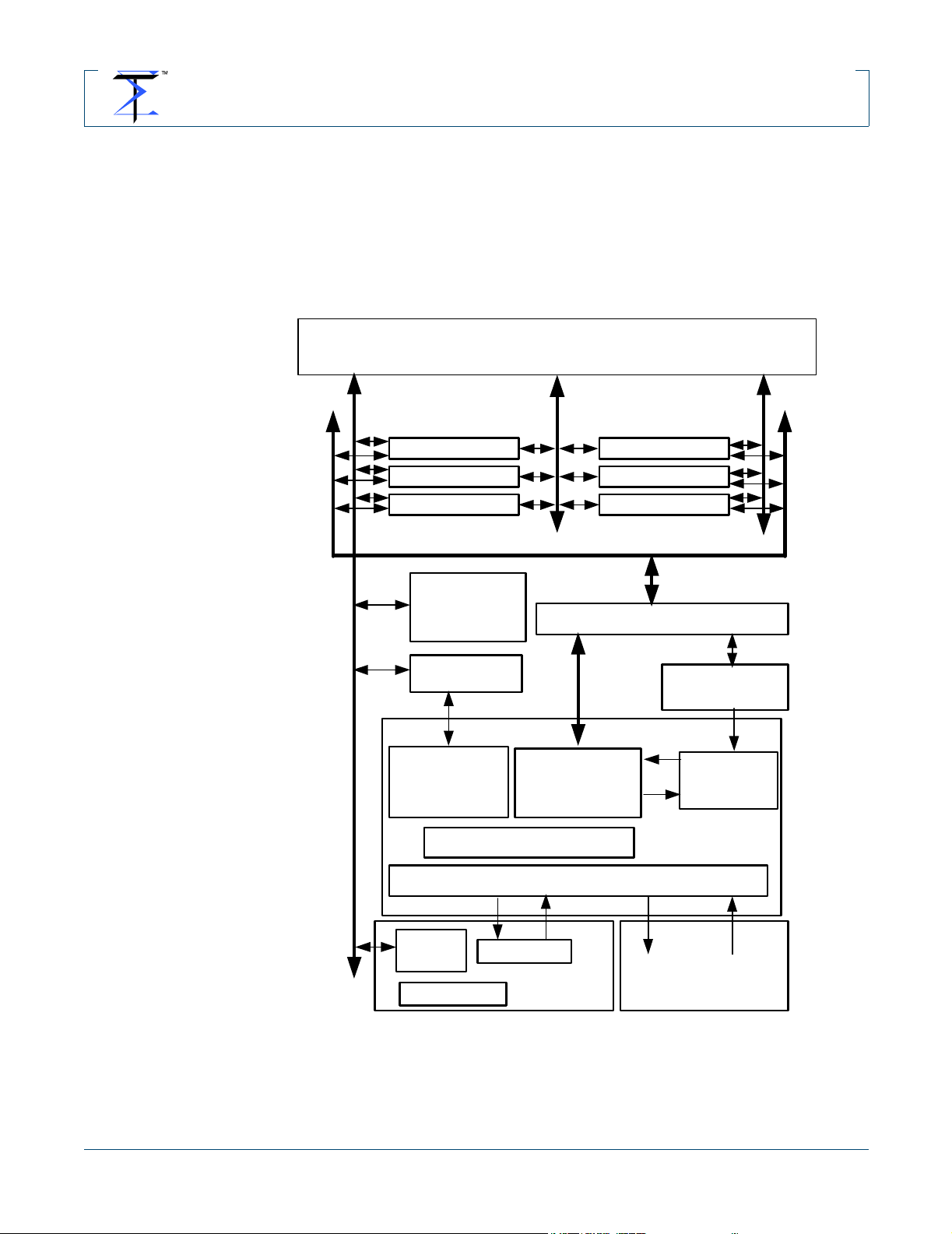
OFFICIAL PRODUCT DOCUMENTATION 8/10/04
STMP35xx
D-Major™Audio System on Chip
hubs running in the USB 2.0 High Speed mode at 480Mbit/second. It can be
attached to USB 2.0 Full Speed interfaces at 12Mbit/second. Of course, the USB
2.0 Full Speed mode allows the STMP35xx to attach to USB 1.1 compliant hosts
and hubs.
The USB interface is used to download digital music data or program code into
external memory and to upload voice recordings or MP3 encoded recordings from
external memory to the PC. Program updates can also be loaded into the flash
memory area using the USB interface.
DSP CORE
X-BUS
16KWord SRAM
16KWord SRAM
16KWord SRAM
DMA-BUS
USB System
Programmable
Registers
Bus Interface
USB Controller
Programmable
Registers
P-BUS
End Point
Controller
Protocol Lay er
Y-BUS
16KWord SRAM
16KWord SRAM
16KWord SRAM
USB DMA Interface
USB Config
State Machine
End
Point
Info
ARC USB 2.0
Device Controller
Serial Interf ac e E ngine
PHY
Regs.
480MHz PLL
Figure 9. USB Interface Block Diagram
The Universal Serial Bus (USB) is a cable bus that supports data exchange
between a host computer and a wide range of simultaneously accessible peripherals. The attached peripherals share USB bandwidth through a host-scheduled,
5-35xx-D1-1.06-071604 13
USB Xcvr
Integrated
USB 2.0 PHY
External USB 2.0
UTMI PHY
Page 14
OFFICIAL PRODUCT DOCUMENTATION 8/10/04
STMP35xx
D-Major™Audio System on Chip
token based protocol. The bus allows peripherals to be attached, configured, used
and detached while the host and other peripherals are in operation.
The USB subsystem is designed to make efficient use of system resources within
the SMTP35xx. It contains a random access DMA engine that reduces the interrupt
load on the DSP and reduces the total bus bandwid th that must be dedicate d to servicing the eight on-chip physical endpoints
It is a dynamically configured port which can suppor t up to 6 general use physical
endpoints and 8 logical endpoints, each of which may be configured for bulk, interrupt or isochronous transfers. The USB configuration information is read from onchip memory via the USB controller’s DMA.
Figure 9 shows a block diagram of the USB controller. This device makes extensive
use of the DMA to read and write the multiple buffers associated with all of the endpoints that it can have open at one time
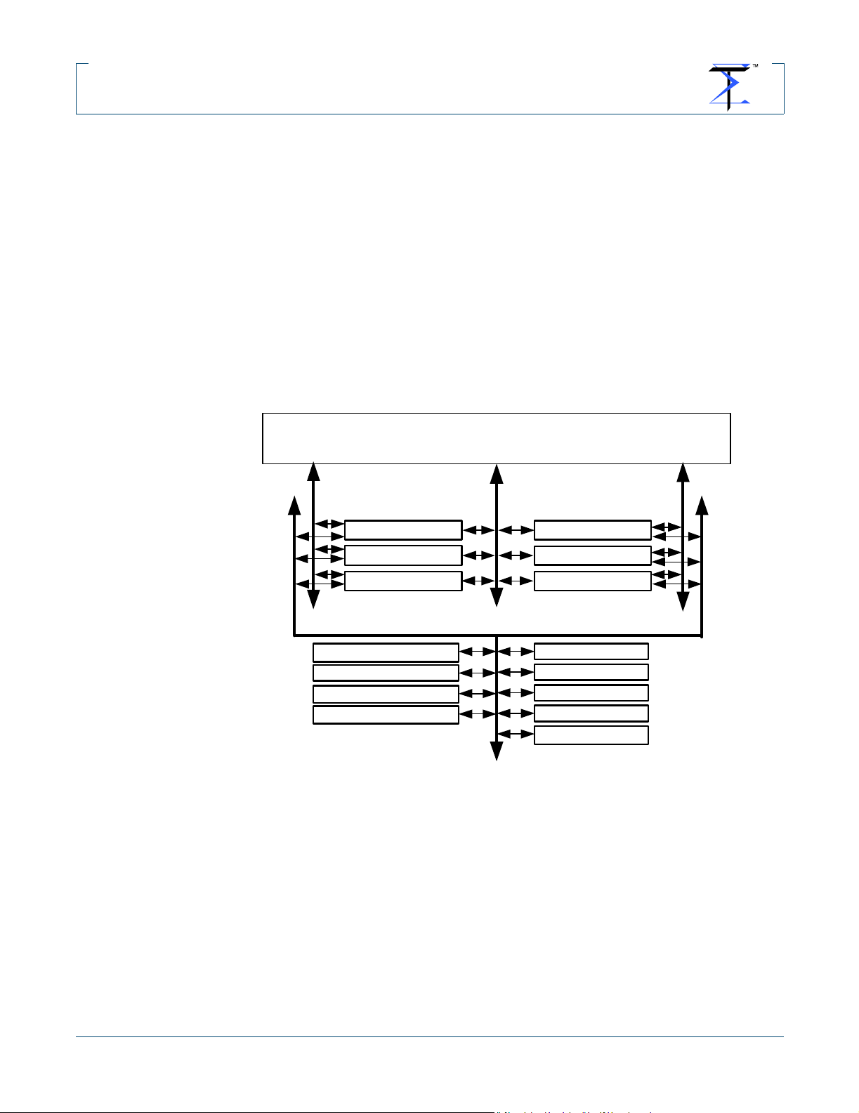
2.3.6. External Memory Interfaces.
DSP CORE
X-BUS
16KWord SRAM
16KWord SRAM
16KWord SRAM
DMA-BUS
EMC
Programmable
Registers
EMC
NAND Flash/
SmartMedia
State Machine
Figure 10. External Memory Controller
The chip includes an external memory controller that has two major functional
modes: SmartMedia/NAND and CompactFlash. The SmartMedia/NAND flash interface provides a state machine that provides all of the logic necessary to perform
DMA functions between on-chip RAM and the flash. The CompactFlash interface
supports the CompactFlash M emory mode. This mode can be used to communicate
with standard CompactFlash (CF) devices such as CF Flash and the IBM MicroDrive. The CF Memory mode can be used to communicate with standard
ATA/ATAPI devices like CD-ROM and hard drives
P-BUS
16KWord SRAM
16KWord SRAM
16KWord SRAM
EMC
DMA Engine
EMC
Compact Flash
State Machine
Y-BUS
14 5-35xx-D1-1.06-071604
Page 15

OFFICIAL PRODUCT DOCUMENTATION 8/10/04
STMP35xx
D-Major™Audio System on Chip
The external memory controller can be described as three fairly independent
devices in one: a SmartMedia/NAN D flash interfac e based on th e STMP3410 flash
controller, a CompactFlash/NOR flash/IDE interface, and a new general purpose
flash state machine that can support the new 1Gb/die NAND flash devices with
128KByte block erase modes. These interfaces share the same device pins, some
registers and the DMA engine.
The interfaces use memory mapped registers to setup and control the transactions.
Data is always sent through DMA – there are no data registers that correspond to
the interface data bus. Transactions are always started with a kick bit. The interface
sets up the control lines and transfers data to/from the internal RAM. Once the
transaction is complete the interface signals the DSP with either a polled flag or an
interrupt.
2.3.7. Hardware Acceleration for ECC for Robust External Storage
The forward error correction module is used to provide STMP35xx applications with
a reliable interface to various storage media, especially storage media that would
otherwise have unacceptable bit error r at es . T he ECC m od ule co m pr ise s two different error correcting code proces so rs:
• 1-bit correcting Samsung SSFDC (Hamming-code) encoder/decoder.
• 4-symbol correcting (9-bits/symbol) Reed-Solomon encoder/decoder.
The 1-bit hamming code is defined by Samsung for use with all SSSFDC compliant
NAND flash memories. This code is capable of correcting a single incorrect bit over
the block for which the ECC is valid (256 bytes per page).
The purpose of the Reed-Solomon decoder is to process a coded block (data block
followed by “parity” check data) to determine if there is an error and, if there are
errors, where they are located and how to correct them. The purpose of the ReedSolomon encoder is to read a block of 503-symbols from RAM, calculate and
append 8-parity symbols to form a 512-symbol RS-codeword.
The Hamming code error corrector is strong enoug h to detect two bit s in erro r in 256
bytes and to correct 1-bit/256 byte errors. Both of these error correction
encoder/decoders use DMA transfers to move data to and from on-chip RAM completely in parallel with the DSP performing other useful work.
2.3.8. Mixed Signal Audio Subsystem
The STMP35xx contains an integrated high quality mixed signal audio subsystem,
including high quality sigma delta D/A and A/D converters. The D/A is of course the
mainstay of the Audio Decoder/Player product application while the A/D is used for
Voice Record and MP3 Encode applications.
The chip includes a low noise headphone driver that allows it to directly drive low
impedance (8Ω or 16Ω) headphones. The direct drive, or “cap-less” mode removes
the need for large expensive DC blocking capacitors in the headphone circuit. The
headphone power amplifier can detect headphone shorts and report them via the
DSP interrupt system. A digitally programmable master volume control allows user
control of the headphone volume. Annoying clicks and pops are eliminated by zero
crossing updates in the volume/mute circuits and by headphone driver startup and
shutdown circuits.
There is an integrated analog mixer that drives the master volume control programmable gain amplifier. The chip provides for two stereo line level inputs and a mono
microphone input. The microphone circuit has a mono to stereo programmable gain
5-35xx-D1-1.06-071604 15
Page 16
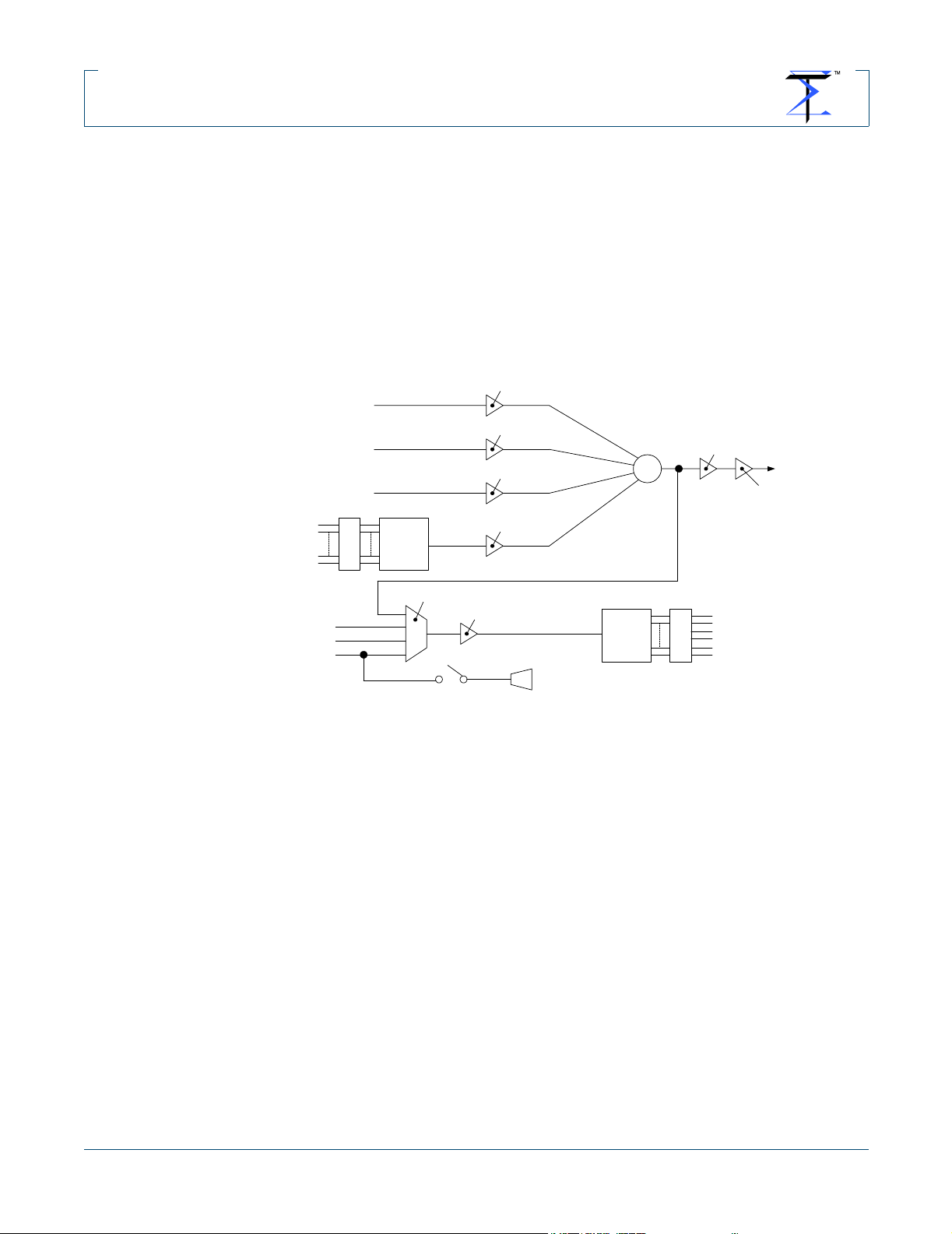
OFFICIAL PRODUCT DOCUMENTATION 8/10/04
STMP35xx
D-Major™Audio System on Chip
pre-amp and an optional microphone bias generator. The line inputs have programmable gain/attenuation and balance capability. The integrated sigma delta DAC has
a programmable gain/attenuation analog amplifier. The programmable gain/attenuation stage outputs from all three stereo inputs and from the DAC are mixed together
to drive the master volume control. There is an analog mux in front of the ADC that
can select any of the three input sources or the mixer output. The se lected source is
then sent to the ADC Gain stage and from there to the ADC. The mixer can be independently powered down. In this configuration, the mixer is bypassed so that the
DAC can still play audio through the headphone driver saving power consumption
and improving the SNR and THD performance.
Line 1 In Gain
LINEIN
Mixer
Master
Volume
Headphone
Driver
FROM
DAC
DMA
MICIN
FMIN
EN
DAC
CLK
Mic In Gain
FM In Gain
DAC Gain
+ OUTPUT
ADC Input Mux
LINEIN
FMIN
MICIN
ADC GAIN
Figure 11. Mixed Signal Audio Elements
2.3.9. Filter Coprocessor
A filter coprocessor has been added to the STMP35xx to reduce th e DSP load associated with filter calculations. Additional enhancements in the ADC and DAC buffer
management have greatly reduced the DSP work load as compared with
STMP3410 based applications. The concomitant reduction in DSP overhead yields
more available MIPS for more intensive software applications or allows the reduction in clock frequency/voltage and thereby dramatically extends the battery life.
The filter coprocessor is a DMA based engine that overlaps execution with the DSP.
2.3.10. IDE/ATA Hard Drive Interface
The external memory controller interface supports the attachment of an ATA/IDE
hard drive device. This is particularly useful for one inch 2GByte hard drive and 2.5
inch 10GByte hard drive MP3 players. Hard drive and external SDRAM configurations are supported in the same application, i.e. large blocks of hard drive data can
be copied to SDRAM leaving the hard drive unused for most of the MP3 play time.
Mic Bias
ADC
CLK
EN
TO
ADC
DMA
2.3.11. SDRAM Interface
The STMP35xx contains an SDRAM controller that can be used to connect external
SDRAM memory chips. The controller is designed to work with 8 bit wide memory
16 5-35xx-D1-1.06-071604
Page 17

OFFICIAL PRODUCT DOCUMENTATION 8/10/04
STMP35xx
D-Major™Audio System on Chip
systems. It supports SDRAM products from the 64Mbit, 128Mbit and 256MBit
JEDEC families. SDRAM memory systems as small as 8MBytes can be configured.
SDRAM memory subsystem are useful for applications that include CD-ROM or IDE
hard drives.
2.3.12. Serial Peripheral Control Interface and I2C
The chip contains a four wire SPI bus. It can act as a master for this bus to control
other chips in the system, such as EEPROMs. It can also act as a slave on this bus
to allow a host processor to communicate with the STMP35xx. The STMP35xx
includes an enhanced SPI interface that provides DMA transfer supp ort. In addition,
the chip contains a two wire SMB/I
master on the SMB interface.
2.3.13. LCD/LED and GPIO
The STMP35xx contains 85 GPIO pins in the 144-pin p ackage. Most digita l pins that
are available for specific functions, e.g. SDRAM interface are also available as
GPIO pins if they are not otherwise used in a particular application.
Most LCD and LED displays can be directly controlled from the GPIO interface.
2
C bus interface. It can act as either a slave or
2.3.14. PULSE WIDTH MODULATOR (PWM) CONTROLLER
The STMP35xx contains four PWM output controllers that can be used in place of
GPIO pins. Applications include LED brightness control and high voltage genera tors
for electroluminescent lamp (E.L.) display back lights. Independent output control of
each phase allows zero, one or hi-Z to be independently selected for the active and
inactive phases. Individual outputs can be run in lock step with guaranteed nonoverlapping portions for differential drive applications.
The controller does not use the DMA. Initial values of Period, Active, and Inactive
widths are set for each desired chan nel. The outputs are selected by phase and
then the desired PWM channels are simultaneously enabled. This effectively
launches the PWM outputs to autonomously drive their loads without further DSP
intervention.
Each PWM channel has a dedicated internal 12 bit counter which increments once
for each divided clock period presented from the clock divider. The internal counter
resets when it reaches the value stored in the channel control registers. The Active
flip flop is set to one when the internal counter reaches the value stored in a register .
It remains high until the internal counter exceeds the value stored in another register. These two value define the starting and ending points for the logically “active”
portion of the waveform. The actual state on the output for each phase, e.g. active
or inactive, is completely controlled by the active and inactive state values in the
channel control registers and can be: HIGH, LOW, or TRI-STATE.
5-35xx-D1-1.06-071604 17
Page 18

OFFICIAL PRODUCT DOCUMENTATION 8/10/04
STMP35xx
D-Major™Audio System on Chip
2.4. STMP35xx Family Members
The STMP35xx is available in a number of ordering options whose function content
is represented in Figure 12, also see 33. “STMP35xx FAMILY MEMBER PART
NUMBERS & ORDERING INFORMATION” on page 391..
STMP3550
‡
STMP3501
STMP350 2
MP3
WMA
LED/LCD Interface
USB Mass Storage
Voice Record
†
FM Tuner
Headphone Amp
& Driver
20-25 Hour
Battery Life
1xAA, 1xAAA Batt.
USB 2.0 (Full Speed)
SLC, MLC NAND
100-pin TQFP
†
STMP3505
STMP3506
MP3
WMA, WMA w/DRM
‡
MP3 Encode
LED/LCD Interface
EL Backlight
USB Mass Storage
RTC [Janus DRM]
Voice Record
FM Tuner
Headphone Amp
& Driver
50 Hour
Battery Life
1,2xAA, 1,2xAAA,
LiIon batteries
USB 2.0 (Full Speed)
SLC, MLC NAND
100-pin TQFP
144-pin BGA
‡
STMP3510
STMP3520
MP3
WMA, WMA w/DRM
‡
MP3 Encode
LED/LCD Interface
EL Backlight
USB Mass Storage
RTC [Janus DRM]
Voice Reco rd
FM Tuner
Headphone Amp
& Driver
50 Hour
Battery Life
1,2xAA, 1,2xAAA ,
LiIon batteries
High-Speed USB 2.0
SLC, MLC NAND
100-pin TQFP
144-pin BGA
‡
STMP3560
MP3
WMA, WMA w/DRM
‡
MP3 Encode
LED/LCD Interface
EL Backlight
USB Mass Storage
SDRAM Interface
RTC [Janus DRM]
Voice Record
FM Tuner
Headphone Am p
& Driver
50 Hour
Battery L ife
1,2xAA, 1,2xAAA,
LiIon batteries
High-Speed USB 2.0
Battery Charging
SLC, MLC NAND
100-pin TQFP
144-pin BGA
Figure 12. STMP35xx Family Members
18 5-35xx-D1-1.06-071604
Page 19
OFFICIAL PRODUCT DOCUMENTATION 8/10/04
STMP35xx
D-Major™Audio System on Chip
2.5. Signal Pin Sharing Among Various Application Configurations
A large number of the chips I/.O pins are shared between various functions. The
exact conflicts can be found in Table 491, “Pin Definition Table,” on page 377.
SDRAM
EMC NAND & SmartMedia
EMC CompactFlash Memory & A TA/IDE
EMC NAND & SmartMedia #2 #1
EMC CompactFlash memory & ATA/IDE #2 #1
SDRAM #1 #1
CapLess Mode Headphone #3
Line In 1 #3
Table 2. Pin Sharing Constraints by Subsystem
NOTES:
#1: The EMC and SDRAM interfaces share a number of pins, including addr ess and
data busses. While precluding exactly simultaneous accesses, careful attention to
chip selects and controller programing allows them to be used within the same
application, e.g. reading CompactFlash in IDE mode and writing SDRAM for H DD
MP3 player applications. Recommendation: use driver level mutual exclusion semaphores.
#2: Within the EMC devices, conflicts can occur between shared pins in the
NAND/SmartMedia interface and the CompactFlash interface. Use driver level
mutual exclusion semaphores.
#3: Capless headphone mode common amplifier output shares a pin with the analog line 1 Right input. In addition, the headphone common mode sense input shares
a pin with analog line 1 Left input. Only one of these uses can be designed into a
specific application.
Line In 1)
CapLess Mode Headphone
2.6. Additional Documentation
Additional documentation and information is available from SigmaTel, including an
extensive software development kit (SDK), application notes, reference schematics,
sample PCB board layouts, sample bill of materials, etc.
It is specifically recommended that the reader refer to the peripheral device include
files from the SDK. These files provide constant declarations for address offsets to
the registers defined in the following sections. Note that the name of each programmable register defined in this data sheet corresponds to a C language #define or
assembly language equate of the exact same name. In addition, these files contain
5-35xx-D1-1.06-071604 19
Page 20

OFFICIAL PRODUCT DOCUMENTATION 8/10/04
STMP35xx
D-Major™Audio System on Chip
declarations that allow symbolic access to the individual bit fields within these registers. User programs can include all of these peripheral include files by simply including the file hw_equ.inc into their assembly files and hw_equ.h into their C files.
20 5-35xx-D1-1.06-071604
Page 21
OFFICIAL PRODUCT DOCUMENTATION 8/10/04
STMP35xx
D-Major™Audio System on Chip
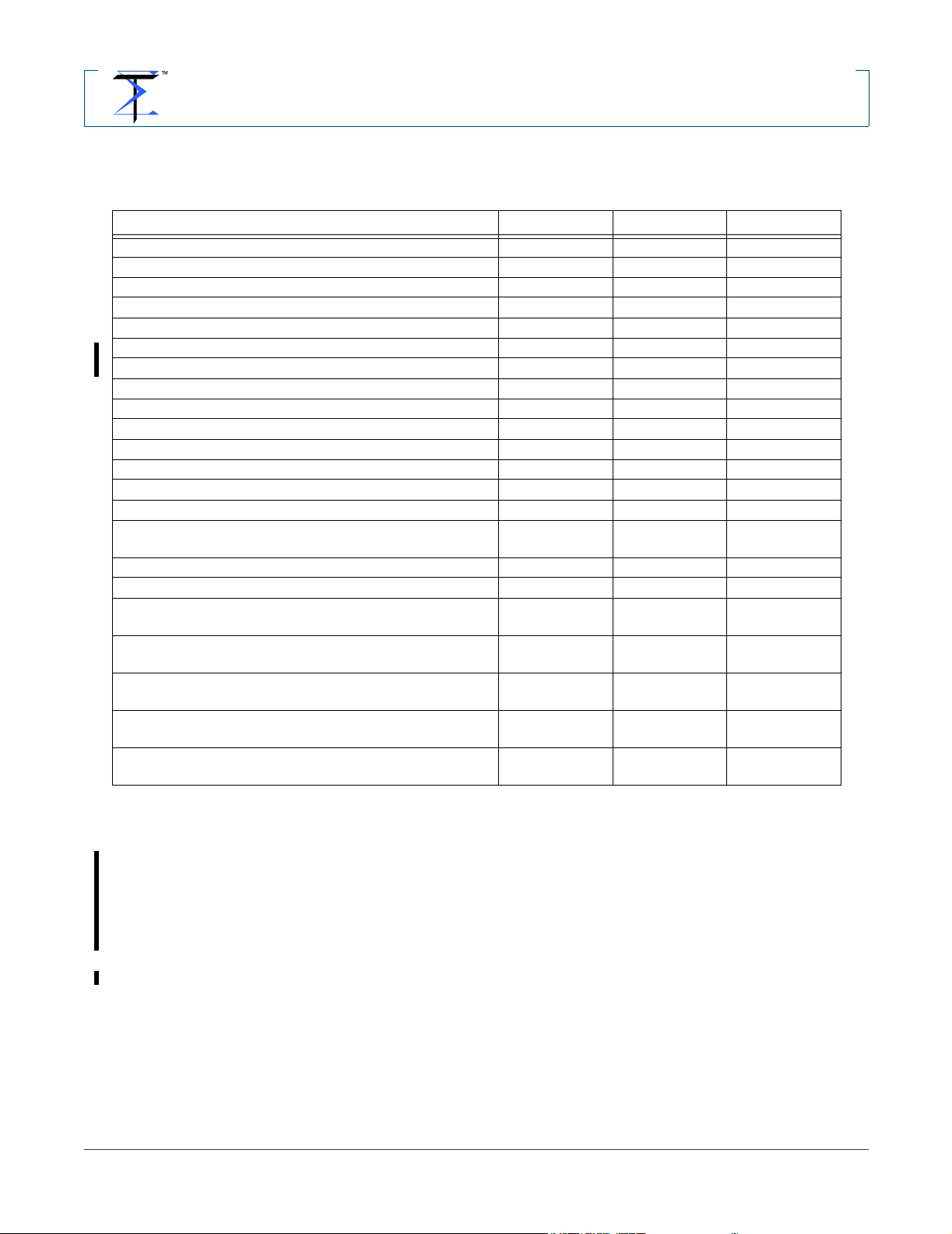
3. CHARACTERISTICS/SPECIFICATIONS
3.1. Absolute Maximum Ratings
PARAMETER MIN MAX UNITS
Ambient operating temperature (Note 1) -10 70 °C
Storage temperature -40 125 °C
Battery Pin (BATT) DCDCMODE 000, 001, 010,011 -0.3 4.2 V
Battery Pin (BATT) DCDCMODE 101,111 -0.3 1.98 V
5 Volt Source Pin (VDD5V) -0.3 5.25 V
PSWITCH DCDCMODE 101,111 -0.3 VddIO V
PSWITCH DCDCMODE 000,001,010,011(Note 2). -0.3 BATT V
Analog supply voltage (VddA1, 2, VddHP, VddPLL) Digital Supply 1.98 V
Digital supply voltage (VddD1, 2, 3) -0.3 Analog Supply V
I/O Supply (VddIO1, 2, 3, 4) -0.3 3.63 V
DCDC converter #1 (DCDC_VddD) -0.3 VddD Rail V
DCDC converter #1 (DCDC_VddA) -0.3 VddA Rail V
DCDC converter #1 (DCDC_VddIO) DCDC Mode 000 -0.3 4.2V V
DCDC converter #1 (DCDC_VddIO) all other DCDC Modes -0.3 3.6V V
DCDC converter #1 (DCDC_Batt) -0.3 max (VddIO,
BATT)
DCDC converter #2 (DCDC2_Vout) DCDC Mode 000 -0.3 4.2 V
DCDC converter #2 (DCDC2_Vout) all other DCDC Modes -0.3 3.6 V
Input voltage on any DCDC MODE input pin relative to
ground (DCDCMOD) (Note 3)
Input voltage on any digital I/0 pin relative to ground (DIO3)
(Note 3)
Input voltage on any digital I/O pin in 1.8V mode relative to
ground (DIO18) (Note 3)
Input voltage on USB D+, D- pins relative to ground (USBIO)
(Note 3)
Input voltage on any analog pin relative to ground (AIO)
(Note 3)
Table 3. Absolute Maximum Ratings
Note: 1. Contact SigmaTel for extended temperature range options. In most systems designs, battery
-0.3 BATT V
-0.3 VDDIO+0.3 V
-0.3 VDDD+0.3 V
-0.3 3.6 V
-0.3 VDDA+0.3 V
and display specifications will limit the operating range to well within these specifications.
2. The maximum voltage limit on the PSWITCH pin can be achieved in DCDCMODE 000, 001, 010, and
011 by connecting the power switch to battery. A 20kohm resistor is placed between the switch and the
PSWITCH pin to limit the current into the pin. In DCDCMODE 111 and 101, the power switch is tied to
VDDIO and a 20kohm resistor is placed between the switch and the PSWITCH pin to limit the current
into the pin. The ESD protection diode limits the input voltage to an acceptable level as long as a 20kohm
resistor is placed in series with PSWITCH pin to limit the current.
3. Pin sets for DCDCMODE, DIO3, DIO18, and AIO are defined in the pin list, see Table 491. “Pin Definition
Table” on page 377.
V
5-35xx-D1-1.06-071604 21
Page 22
OFFICIAL PRODUCT DOCUMENTATION 8/10/04
STMP35xx
D-Major™Audio System on Chip
3.2. Recommended Operating Conditions
PARAMETER MIN TYP MAX UNITS
Digital core supply voltage – VddD1, VddD2, VddD3 (Note 4)
Specification dependent on DSP frequency
Digital I/O supply voltage – VddIO1, VddIO2 2.9 3.0 3.6 V
Analog supply voltage – VddA(VddA1, VddA2, VddA3) for
player type applications where the mixer is powered down.
Specification dependent on maximum output power
Analog supply voltage – VddA(VddA1, VddA2, VddA3) for FM
or Voice Record type applications which utilize the mixer.
Specification dependent on maximum output power
Battery startup input voltage in 1xAA or 1xAAA mode 0.9 - - V
Full Scale Input Voltage:
Line Inputs (Note 5) - 0.6 - Vrms
Mic Input
With 20 dB boost
Without 20 dB boost
Full Scale Output Voltage with 16Ω load:
Headphone/Line Outputs (VddA = 1.8 V) - 0.54 - Vrms
Headphone/Line Outputs (VddA = 1.38 V) - 0.42 - Vrms
Crosstalk between output channels (16Ω loads at 1Khz) - -75 - dB
THD+N (16Ω headphone at 1 Khz) except STMP3501
(Note 9)
THD+N (10KΩ load at 1 Khz) -87 dB
THD+N (16Ω headphone at 1 Khz) for STMP3501 -64 dB
Analog line input resistance (Note 6) - 25 - kΩ
Microphone input resistance - 10 0 - kΩ
Analog output resistance - - <1 Ω
DAC SNR Idle Channel (Note 7) - 96 - dB
DAC -60dB dynamic range (Note 7) 92 94 - dB
ADC SNR Idle Channel (Note 7) 90 dB
ADC -60dB dynamic range (Note 7) 90 dB
Line SNR (Note 7) except STMP3501 92 94 - dB
Line SNR (Note 7) for STMP3501 87 89 - dB
Standby Current (Note 8) 150 200 uA
Table 4. Recommended Operating Conditions
Note: 4. Recommended operating voltages for DCLK can be found in Table 5 In all cases, design must allow for
board and bypass design variations.
5. At 1.38VddA max input is 0.45Vrms
6. Input resistance changes with volume setting: 10KΩ at +12dB, 25KΩ at 0dB, 50KΩ at -34.5dB
7. Measured “A weighted” over a 20 Hz to a 20 kHz bandwidth, relative to full scale output voltage (1.8V)
8. The chip consumes current when in the “OFF” mode to keep the crystal oscillator and the real time clock
running. With a typical 2850mAh AA battery, the standby current would take more than 1 year to drain the
battery fully . It also is possible to design a system that disables the crystal oscillator and real time clock to
achieve a much lower OFF current.
9. The BGA package reduces THD performance by approximately 4dB.
1.35 - Analog
Supply
Digital
Supply
1.45 - 1.98 V
-
--70-66dB
-1.98V
- Vrms
0.06
0.6
V
22 5-35xx-D1-1.06-071604
Page 23
OFFICIAL PRODUCT DOCUMENTATION 8/10/04
STMP35xx
D-Major™Audio System on Chip
The following table can be used to select a proper setting for VddD and VddD
brownout voltages based on standar d analysis of worst case design and characterization data.
MAX
DCLK
TARGET
75.6MHz 1.92 V 11100 1.85 V 11010
69.6MHz 1.82 V 11001 1.76 V 10111
64.8MHz 1.73 V 10110 1.66 V 10100
60.0MHz 1.63 V 10011 1.54 V 10000
48.0MHz 1.4 V 01100 1.34 V 01010
39.6MHz 1.37 V 01011 1.28 V 01000
Min.
VddD
Table 5. Recommended Operating Conditions for sp ecific dclk targets
HW_DCDC_VDDD_
VOLTAGE_LEVEL
Corresponding
VddD
Brownout Voltage
HW_DCDC_VDDD_
BROWNOUT_LEVEL
.
5-35xx-D1-1.06-071604 23
Page 24
OFFICIAL PRODUCT DOCUMENTATION 8/10/04
STMP35xx
D-Major™Audio System on Chip
3.3. DC Characteristics
PARAMETER MIN TYP MAX UNITS
Power Dissipation, VddD = 1.37 V, VddA = 1.37 V, VddIO =
3.05 V DCDC mode = 2-Channel Boost, DCLK = 36 MHz on
PLL, USB off, Application = MP3 Play, minimum power
configuration selected.
V
(DIO3) - Input high voltage for DIO3 digital I/O pin set, in
iH
3.3 Volt mode.
V
(DIO3) - Input low voltage for DIO3 digital I/O pin set in 3.3
IL
Volt mode.
V
(DIO18) - Input high voltage for DIO18 digital I/O pin set in
IH
1.8 Volt mode.
(DIO18) - Input low voltage for DIO18 digital I/O pin set in
V
IL
1.8 Volt mode.
V
(DIO3) - Output high voltage for DIO3 digital I/O pin set in
OH
3.3 Volt mode, 4mA mode.
V
(DIO3) - Output high voltage for DIO3 digital I/O pin set in
OH
3.3 Volt mode, 8mA mode.
(DIO3) - Output low voltage for DIO3 digital I/O pin set in
V
OL
3.3 Volt mode.
V
(DIO18) - Output high voltage for DIO18 digital I/O pin
OH
set in 1.8 Volt mode.
V
(DIO18) - Output low voltage for DIO18 digital I/O pin set
OL
in 1.8 Volt mode.
Table 6. DC Characteristics
2.0 V
0.7*VddD V
0.8*VddIO V
0.8*VddIO V
VddD - 0.4 V
80 mW
0.8 V
0.3*VddD V
0.4 V
0.4 V
3.4. Restrictions on Approved Usage of SigmaTel Parts
SigmaTel Products are not designed or intended for use in life support appliances,
or systems where malfunction of a SigmaTel product can reasonably be expected to
result in personal injury or death nor are they intended for use in any application
where malfunction of a SigmaTel product can reasonably be expected to result in
environmental or other subsequent damage.
24 5-35xx-D1-1.06-071604
Page 25
OFFICIAL PRODUCT DOCUMENTATION 8/10/04
STMP35xx
D-Major™Audio System on Chip
4. DSP CORE
The on-chip DSP core is modeled exactly after the Motorola DSP56004. It supports
the identical instruction set, registers, addressing modes, etc., as the DSP56000
family of digital signal processors. Figure 13 shows the DSP architecture.The DSP
core is a general-purpose 24-bit DSP especially suited to high fidelity digital audio
applications for very low power/energy environments.
OnCE
Debugger
Interface
Data
Bus
Switch
ADDRESS
GENERATION
UNIT
ON-CHIP
PROGRAM
RAM/ROM
XAB
YAB
PAB
XDB
YDB
PDB
GDB
ON-CHIP
Y
RAM
ON-CHIP
X
RAM
Peripherals
PROGRAM
Interrupt
Controller
5-35xx-D1-1.06-071604 25
PROGRAM
DECODE
CONTROLLER
Mode GPIO bits
IVL[6:0],IRQA, IRQB, NMI
RESET
Figure 13. DSP Architecture
PROGRAM
ADDRESS
GENERATOR
DATA ALU
24 x 24 +56 --> 56-bit M AC
Two 56 bit Accumulators
Page 26

OFFICIAL PRODUCT DOCUMENTATION 8/10/04
STMP35xx
D-Major™Audio System on Chip
The central components are:
• Data Busses (XD,YD,PD)
• Address Busses (XA,YA,PA)
• Data Arithmetic Logic Unit (Data ALU)
• Address Generation Unit (AGU)
• Program Control Unit (PCU)
• On-Chip Program ROM
• On-Chip X,Y,P RAM
• On-Chip Emulation circuitry
The DSP is organized around the registers of three independent e xecution unit s: the
PCU, the AGU and the data ALU. Data movement between the execution units
occurs over four bidirectional 24-bit buss es: the X data bus (XDB), the Y data bus
(YDB), the program data bus (PDB) and the global data bus (GDB). Certain instruc tions treat the X and Y data buses as one 48-bit data by concatenating them. Data
transfers between the data ALU and the X data memory or Y data memory occu r
over the XDB and YDB respectively.
The bus structure supports general register-to-register, register-to-memory, and
memory-to-register data movement. It can transfer up to two 24-bit words or one 56bit word in the same instruction cycle.
Transfers between busses occur in the internal bus switch. The internal bus switch,
which is similar to a switch matrix, can connect any two internal busses without adding pipeline delays. Thus greatly simplifying the programming model.
The bit manipulation unit is located in the bus switch so that it can access each
memory space. The bit manipulation un it performs bit operations on memory locations, address registers, control registers and data regi sters over the XDB, YDB and
GDB.
The data ALU performs all of the arithmetic and logical operations on data operands. It consists of four 24 bit input registers, two 48-bit accumulators and two 8-bit
accumulator extension registers, an accumulator shifter, two data bus shifter/limiter
circuits, and a parallel single cycle, non-pipelined multiply-accumulator (MAC) unit.
The address generation unit (AGU) performs all of the ad dress storage and address
generation computations necessary to indirectly address data operands in memory.
It operates in parallel with other DSP resources to minimize address generation
overhead and keep the su pply of da ta operand s fed to the da ta ALU. The A GU has
two identical address arithmetic units that can generate two 16-bit addresses every
instruction cycle. Each of the arithmetic units can perform one of three types of
address arithmetic: linear, modulo and reverse-carry.
The program control unit performs instruction prefetch, instruction decode, hardware DO loop control, and interrupt/exception processing. It consists of three components: the program address generator, the program decode controller, and the
program interrupt controller. It contains a 15-level by 32 bit system stack memory
and the following directly addressable registers: the program counter (PC), loop
address (LA), loop counter (LC), status register (SR), and the operating mode register (OMR).
The DSP core responds to 7 interrupt vector level inputs (IVL[6:0], two peripheral
interrupts (IRQA, IRQB) and a non-maskable interrupt (NMI).
26 5-35xx-D1-1.06-071604
Page 27
OFFICIAL PRODUCT DOCUMENTATION 8/10/04
STMP35xx
D-Major™Audio System on Chip
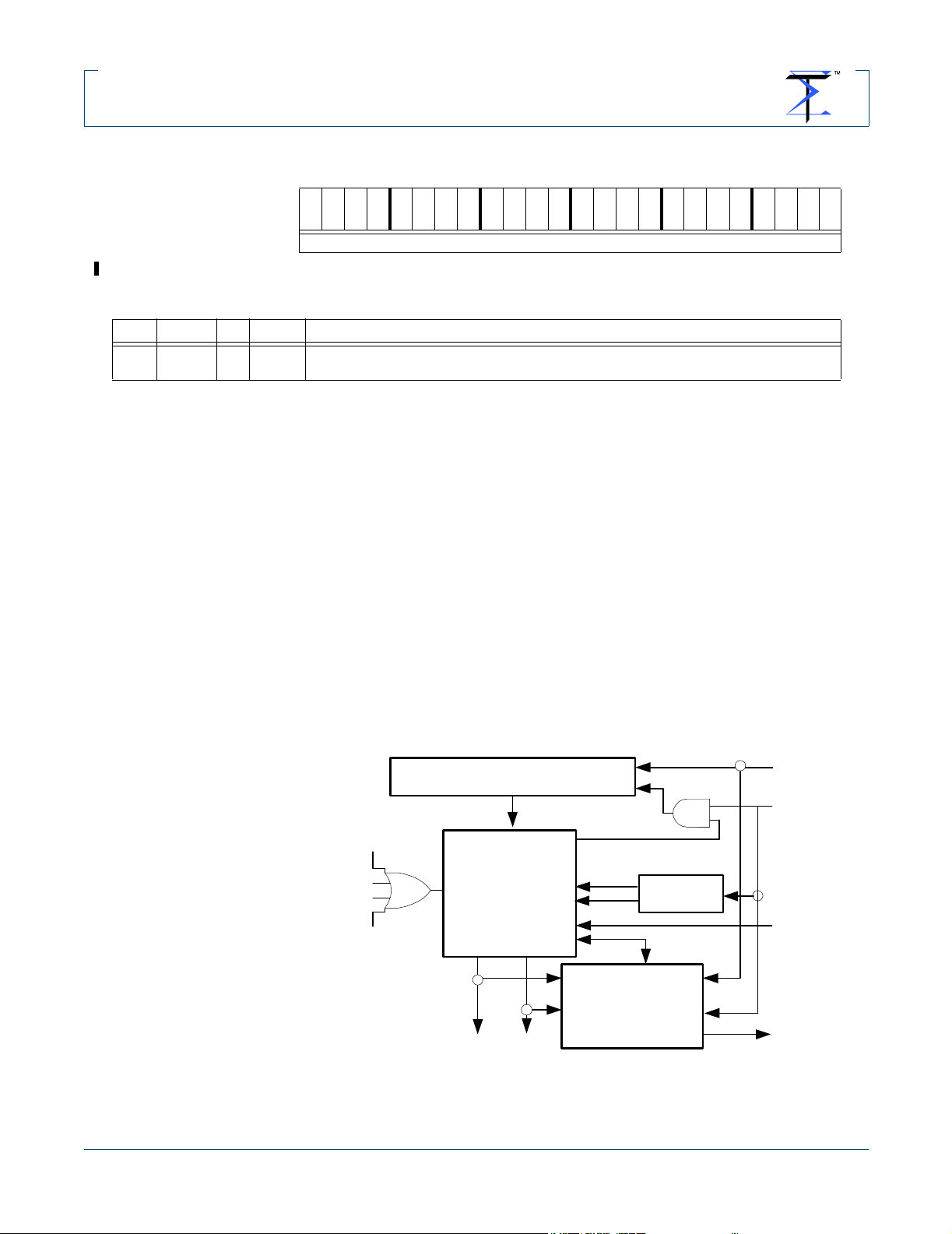
4.1. Operating Mode Register
The organization of the operating mode register is shown below. The operating
mode register determines chip configuration including boot modes, and memory
configuration. The HW_OMR is a core register that is accessible by special DSP
instructions. It therefore has no address.
HW_OMR SPECIAL
BITS LABEL RW RESET DEFINITION
23:8 RSRVD R0 Reserved – Must be written with 0.
7 RSRVD R 0 Reserved – Must be written with 0.
6 SD RW 0 Stop Delay – This bit is exported from the core as an output. It can be used when
waking up from the STOP low power standby mode. If this bit is set, then when an
IRQA interrupt occurs to wake up the core from the STOP state, the clock control
circuitry will wait a time period (e.g. 65536 clock cycles) before allowing the clocks
back in to the DSP core. This can be used, for example, to restabilize a PLL clock
oscillator. If this bit has a zero value, then the clocks will be allowed back into the core
immediately after the occurrence of the IRQA interrupt, thus implementing a “warm
boot” from the STOP low power standby state.
5 RSRVD R 0 Reserved – Must be written with 0.
4 MC RW GP0 Operating Mode C – This bit is used to configure the boot mode for the STMP35xx.
When the hardware reset is active, this bit samples the state of GP0 pin. Once the
boot code executes, it can check the state of this bit in order to make decisions about
what type of boot mode to perform.
3:2 RSRVD R 0 Reserved – Must be written with 0.
1 MB RW GP1 Operating Mode B – This bit is used to configure the boot mode for theSTMP35xx.
When the hardware reset is active, this bit samples the state of the GP1 pin. Once the
boot code executes, it can check the state of this bit in order to make decisions about
what type of boot mode to perform.
0 MA RW 1 Operating Mode A – This bit is used to choose between Boot ROM and Program
Memory for instruction fetches and read accesses. When this bit is set, as it is after
hardware reset, the Boot ROM space is activated and any fetches or read accesses to
the P: space will refer to the on-chip ROM. When this bit is a zero, the Program RAM
Memory space is enabled instead of the Boot ROM memory space and any fetch or
read access to P: space will refer to the on-chip RAM. Writes to P: space always
access the program RAM regardless of the state of the MA bit. It is not possible to
write to the program ROM. This bit affects ROM access in region P:$0000 through
P:$3FFF. Accesses to the high mapped region of ROM, P:$C000 through P:$FFFF is
controlled by HW_RAM_ROM_CFG_PROMIE.
Table 7. Operating Mode Register Description
4.2. General Debug Register
The HW_GDBR Register is also mapped into the X Peripheral I/O space. This register is used as a gateway between the DSP and the Debug port. For instance, when
displaying the states of the internal registers and memory of the DSP core, the DSP
moves the data to this register and the data is then shifted out the OnCE_DSO pin.
The HW_GDBR register operation is controlled automatically by the emulator and
the debug circuitry within the core. An added feature of the Debug Unit is that the
emulator cannot access the debug unit unless a write to the HW_GDBR Register is
executed by the DSP (normally in the boot code).
5-35xx-D1-1.06-071604 27
Page 28
OFFICIAL PRODUCT DOCUMENTATION 8/10/04
K
N
STMP35xx
D-Major™Audio System on Chip
HW_GDBR X:$FFFC
23222120191817161514131211100908070605040302010
VALUE
Table 8. HW_GDBR
BITS LABEL RW RESET DEFINITION
23:0 VALUE RW 0 Value to be read by the debugger or debugger value to be read by a DSP instruction
from the debugger.
Table 9. General Debug Register (GDBR)
4.3. OnCE (On-Chip Emulator) Debug Interface
The DSP on-chip emulation (OnCE) circuitry provides a sophisticated debugging
tool that allows simple, inexpensive, and speed independent access to the processor’s internal registers, memories and peripherals. OnCE provides software engineers with access to the internal state including the addresses of the last five
instructions and provides the ability to modify that state, and single step the processor. OnCE capabilities are accessed through a four pin interface
1. Debug Serial input (OnCE_DSI)
2. Debug Serial Clock (OnCE_DSK)
3. Debug Serial Output (OnCE_DSO)
4. Debug Request Input (OnCE_DRN)
The OnCE controller and serial interface consists of the following blocks: OnCE
command register, bit counter, OnCE decoder and the status/control register. For a
block diagram, see Figure 14. “OnCE Interface Block Diagram” on page 28.
0
OnCE COMMAND REGISTER
ISBKPT
ISDR
ISTRACE
ISSWDBG
Figure 14. OnCE Interface Block Diagram
28 5-35xx-D1-1.06-071604
OnCE
DECODER
REG
READ
WRITE
REG
bit 7
Bit Counter
bit 23
Status and Control
Register
OnCE_DSI
OnCE_DS
OnCE_DR
OnCE_DSO
Page 29
OFFICIAL PRODUCT DOCUMENTATION 8/10/04
STMP35xx
D-Major™Audio System on Chip
The OnCE Command Register is an 8 bit shift register that receives the serial data
from the OnCE_DSI pin. It holds the 8 bit commands to be used as input for the
OnCE controller.
OnCE Command Register
BITS LABEL RW RESET DEFINITION
7 RW RW The read/write bit specifies the direction of the data transfer. For zero, write the data
associated with the command into the register specified in the RS field. For one, read
the data contained in the register specified in the RS field.
6 GO RW If the GO bit is set, the chip will execute the instruction which resides in the PIL
register. To execute the instruction, the processor leaves the debug mode, and the
status is reflected on the OS0,OS1 pins. The processor will return to the debug mode
immediately after executing the instruction.
5 EX RW If the Exit Command bit is set, the processor will leave the debug mode and resume
normal operation. The Exit command is executed only if the Go command was issued
and the operation is a write to OPDBR or a read/write to” No Register Selected”.
4:0 RS RW Register Select field
Table 10. OnCE Command Register
The Register Select field (RS[4:0]) selects one of 32 OnCE debug registers to be
read or written.
RS[4:0] REGISTER SELECTED
00000 OnCE Status and Control Register
00001 Memory Breakpoint register
00010 Reserved
00011 Trace Counter
0010X Reserved
00110 Memory Upper Limit
00111 Memory Lower Limit
01000 GDB Register NOTE: this register can be read or written by the DSP instructions
01001 PDB Register
01010 PAB Register for Fetch
01011 PIL register, next instruction from debugger comes from here
01100 Clear Memory Breakpoint Counter
01101 Reserved
01110 Clear Trace Counter
01111 Reserved
10000 Reserved
10001 Program Address Bus FIFO and Increment Counter
10010 Reserved
10011 PAB Register for Decode
101XX Reserved
11XX0 Reserved
11111 No Register Selected
Table 11. OnCE Register Selects
5-35xx-D1-1.06-071604 29
Page 30
OFFICIAL PRODUCT DOCUMENTATION 8/10/04
STMP35xx
D-Major™Audio System on Chip
5. ON-CHIP MEMORY SUBSYSTEM
The chip includes 96 kwords of on-chip RAM (96k x 24 bits = 2.25 Mbits) that is
used for program and data storage, and 16 K word s of on-chip ROM (16K x 24 b it s =
384kbits) that is used for the code that boots the device (see Section 20 for more
details on boot modes and the contents of the on-chip ROM). The on-chip ROM is
mapped at the address range P:$0000-$3FFF at reset, it can also be configured to
be mapped at address range P:$CFFF-$FFFF, or it can be disabled.
The on-chip RAM is organized into two banks of 48K words each, called PXRAM
and PYRAM. PXRAM can be mapped into the DSP P memory space, starting at
P:$0000, or into the DSP X memory space, starting at X:$0000. PYRAM can be
mapped into the DSP P memory space, starting immediately after the end of the
PXRAM memory, or into the DSP Y memory space, starting at Y:$0000. Both
PXRAM and PYRAM memory can be allocated to the DSP P, X or Y memory
spaces in 8K word increments, from a minimum of 0K word s to all available memo ry.
The memory configuration is controlled by the PX & PY Memory Configuration registers documented below. There are no hardware safeguards against improper programming of these registers. It is possible to allocate less than all of the on-chip
RAM, unallocated memory will then be invisible to the DSP.
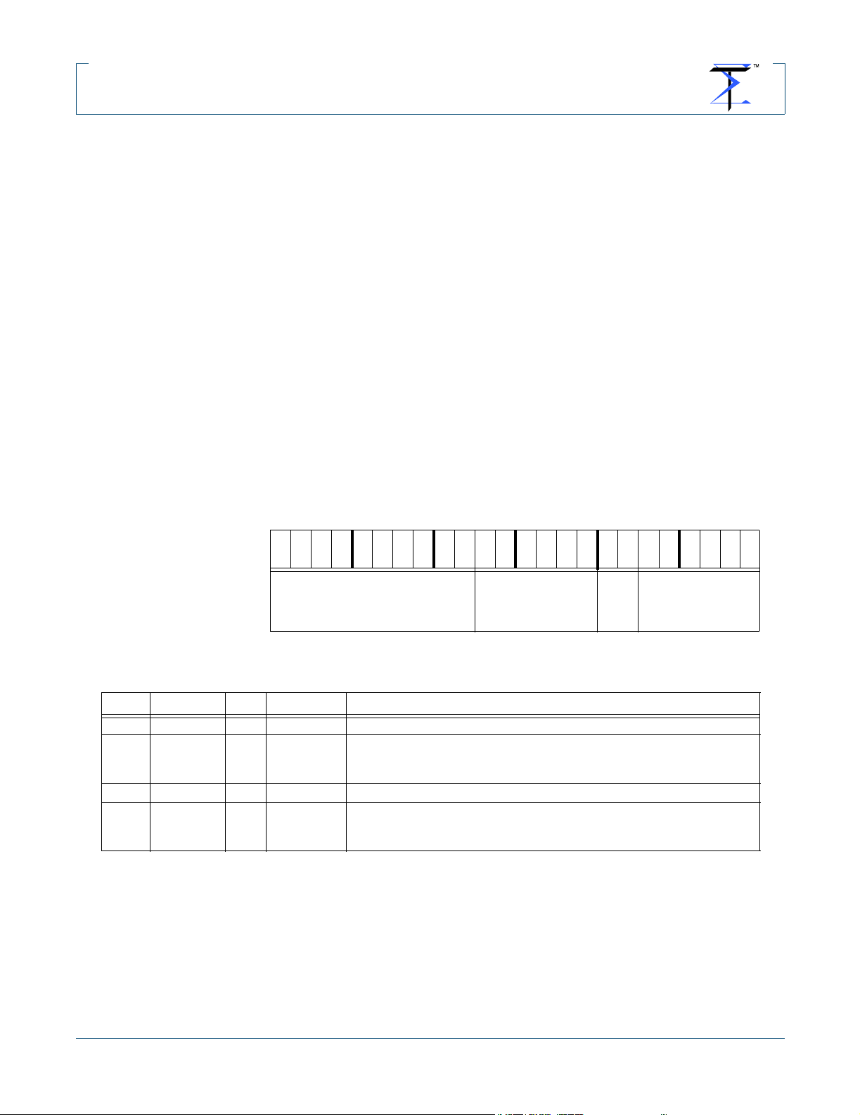
5.1. PXRAM Configuration Register
HW_PXCFG X:$FFE8
23222120191817161514131211100908070605040302010
PXXSIZE
Table 12. HW_PXCFG
BITS LABEL RW RESET DEFINITION
23:14 RSRVD R0 Reserved – Must be written with 0.
13:8 PXXSIZE RW 011000 Number of kwords of PXRAM that is mapped in the DSP X memory
space. Initialize 24KW to X RAM. This six bit field represents 1K
increments of RAM. It must be allocated in 8K word chunks.
7:6 RSRVD R0 Reserved – Must be written with 0.
5:0 PXPSIZE RW 011000 Number of kwords of PXRAM that is mapped in the DSP P memory
space. Initialize 24KW to Y RAM. This six bit field represents 1K
increments of RAM. It must be allocated in 8K word chunks.
Table 13. PXRAM Configuration Register Description
PXPSIZE
0
30 5-35xx-D1-1.06-071604
Page 31

OFFICIAL PRODUCT DOCUMENTATION 8/10/04
STMP35xx
D-Major™Audio System on Chip
5.2. PYRAM Configuration Register
HW_PYCFG X:$FFE9
23222120191817161514131211100908070605040302010
0
PYYSIZE
Table 14. HW_PYCFG
BITS LABEL RW RESET DEFINITION
23:14 RSRVD R0 Reserved – Must be written with 0.
13:8 PYYSIZE RW 011000 Number of kwords of PYRAM that is mapped in the DSP Y memory
space. Initialized to 24KW Y RAM.This six bit field represents 1K
increments of RAM. It must be allocated in 8K word chunks.
7:6 RSRVD R0 Reserved – Must be written with 0.
5:0 PYPSIZE RW 011000 Number of kwords of PYRAM that is mapped in the DSP P memory
space. Initialized to 24KW to P RAM. This six bit field represents 1K
increments of RAM. It must be allocated in 8K word chunks.
Table 15. PYRAM Configuration Register Description
PYPSIZE
The PXRAM bank is accessible to DSP P space accesses, DSP X space accesses,
and DMA accesses. The PYRAM bank is accessible to DSP P space accesses,
DSP Y space accesses, and DMA accesses. PXRAM & PYRAM are made up of 3
physical blocks of 16K words each for a total of 48K words each. Since the allocation of on-chip RAM to DSP P space, X space, & Y space is in 8K Word increments,
it is possible for a single physical memory block in the PXRAM bank to be accessed
by the DSP P, DSP X, and DMA busses at the same time, similarly for the PYRAM
bank. When this happens, the memory interface control logic steals one or more
clock cycles from the DSP to allow all of the accesses to complete in separate clock
cycles. In case of conflict, DMA accesses take priority over DSP accesses, and DSP
program accesses take priority over DSP data accesses.
It is possible to eliminate cycle steals because of DSP P space and DSP X or Y conflicts by allocating PXRAM & PYRAM in increments of 16K words, this means that
each physical memory block is allocated to DSP P , X or Y sp ace. It is not possible to
eliminate the cycle steal that happens because a DMA access conflicts with a DSP
access to memory. In order to allow the programmer to monitor total number of
cycle steals are happening, the contents of the Cycle Steal Count Register
(HW_CYCSTLCNT) will increment whenever a cycle is stolen for a memory access
conflict.
Figure 15 below shows an example of how the PXRAM and PYRAM memory banks
can be allocated. In this example, PXRAM is allocated as 24K words P, &
5-35xx-D1-1.06-071604 31
Page 32

OFFICIAL PRODUCT DOCUMENTATION 8/10/04
STMP35xx
D-Major™Audio System on Chip
24K words X, and PYRAM is allocated as 24K words P, & 24K words Y, for a total of
48K words of P, 24K words of X, and 24K words of Y.
PYMEM
Y:$0000
Y:$1FFF
Y:$2000
24kwords
Y memory
from PYRAM
Y:$3FFF
Y:$4000
Y:$5FFF
P:$BFFF
P:$A000
24 kwords
X memory
from PXRAM
PXMEM
X:$0000
X:$1FFF
X:$2000
X:$3FFF
X:$4000
X:$5FFF
P:$5FFF
P:$4000
physical:$BFFF
48 kwords
total per
memory
bank
8 kwords
per
instance
8 kwords
per
instance
8 kwords
per
instance
8 kwords
per
instance
24 kwords
P memory
from PXRAM
P:$2000
P:$0000
8 kwords
per
instance
8 kwords
per
instance
physical:$0000
24 kwords
P memory
from PYRAM
P:$8000
P:$6000
Figure 15. On-Chip RAM Organization
When the memory is configured as shown in Figure 15, the DSP’s view of the memory map will be as shown below in Figure 16. The DSP P address space has 48K
words of RAM as shown in the range P:$0000 to P:$BFFF. If the ROM is enabled
then it appears in the DSP P address space at P:$C000 to P:$FFFF. The DSP X
space has 24K words of RAM at X:$0000 to X:$5FFF, likewise th e DSP Y space has
24K words of RAM at Y:$0000 to Y:$5FFF. The address ranges X:$6000 to
X:$EFFF, and Y:$6000 to Y:$FFFF are not populated with any memory. The
address range P:$C000 to P:$FFFF is unpopulated if the ROM is not enabled. The
address range X:$F000 to X:$FFFF is reserved for on-chip peripherals.
In the above example memory configuration, it is possible for cycle steals to happen
because of either DSP access conflicts, or because of DMA access conflicts. The
areas in the memory map where DSP access conflicts can occur are cross hatched
in Figure 16. If the DSP attempts to access an address in the range P:$4000 to
P:$5FFF at the same time as an address in the range X:$4000 to X:$5FFF, a stall
cycle will occur. If the DSP attempts to access an address in the range P:$A000 to
32 5-35xx-D1-1.06-071604
Page 33

OFFICIAL PRODUCT DOCUMENTATION 8/10/04
STMP35xx
D-Major™Audio System on Chip
P:$BFFF at the same time as an address in the range Y:$4000 to Y:$5FFF, a stall
cycle will also occur.
64 kwords
total
16 kwords
from PROM
24 kwords
from PYMEM
24 kwords
from PXMEM
DSP
P space
P:$FFFF
P:$C000
P:$BFFF
P:$A000
P:$9FFF
P:$8000
P:$7FFF
P:$6000
P:$5FFF
P:$4000
P:$3FFF
P:$2000
P:$1FFF
24 kwords
from PXMEM
DSP
X Space
X:$FFFF
peripherals
X:$F000
not
populate d
X:$6000
X:$5FFF
X:$4000
X:$3FFF Y:$3FFF
X:$2000
X:$1FFF Y:$1FFF
24 kwords
from PYMEM
DSP
Y space
Y:$FFFF
not
populate d
Y:$6000
Y:$5FFF
Y:$4000
Y:$2000
It is possible to reallocate on-chip RAM at any time, however doing so is dangerous
and should be done carefully. In particular, the DSP P space memory that is allocated from the PYMEM memory bank will move within the P address space if the
allocation of PXRAM memory is changed.
5.3. On-Chip ROM
When the chip comes out of reset, the OMR MODE A bit is set to one, see 4.1.
“Operating Mode Register” on page 27. This bit, when set to one, enables the OnChip ROM to be read instead of whatever PXRAM or PYRAM is assigned to the first
16KW of the P address space, i.e. P:$0000 through P:$3FFF. For the default
PXRAM/PYRAM allocation described above, the cross hatched region of Figure 17
shows the 16KW of PXRAM space that are overla id by ROM. Whenever a P space
access is made in the range P:$0000 through P:$3FFF, AND OMR_MODE_A =1
AND a read cycle is performed, then ROM data is presented to the DSP P-bus. If
mode A is not set then reads in this range access the alloca ted PXRAM data. Wh enever a P-bus write cycle is performed within this address range it is always directed
P:$0000
Figure 16. DSP Memory MAP
X:$0000
Y:$0000
5-35xx-D1-1.06-071604 33
Page 34

OFFICIAL PRODUCT DOCUMENTATION 8/10/04
STMP35xx
D-Major™Audio System on Chip
to PXRAM. Thus at power on time, Instructions and P-space read data are read
from the On-Chip ROM while P-space write data is written to the PXRAM.
OMR_MODE_ A =0 & READ
& HW_RAM_ROM_CFG_ROMIE =1
64 kwords
total
16 kwords
from PROM
24 kwords
from PYMEM
24 kwords
from PXMEM
DSP
P space
P:$FFFF
P:$C000
P:$BFFF
P:$A000
P:$9FFF
P:$8000
P:$7FFF
P:$6000
P:$5FFF
P:$4000
P:$3FFF
P:$2000
P:$1FFF
P:$3FFF
16KW
ROM
24 kwords
from PXMEM
DSP
X Space
X:$FFFF
peripherals
X:$F000
not
populate d
X:$6000
X:$5FFF
X:$4000
X:$3FFF Y:$3FFF
X:$2000
X:$1FFF Y:$1FFF
24 kwords
from PYMEM
DSP
Y space
Y:$FFFF
not
populate d
Y:$6000
Y:$5FFF
Y:$4000
Y:$2000
P:$0000
P:$0000
X:$0000
OMR_MODE_ A =1 & READOMR_MODE_ A =0 | WRITE
Y:$0000
Figure 17. DSP Memory MAP with On-Chip ROM
The boot strap code, which begins execution in the on-chip ROM takes advantage
of these mode settings as follows: The boot code reads the new program code in
from the NAND Flash, or other source. It copies the data, as described in the boot
mode section below, to the appropriate memory locations. If a block is copied to Pspace in the range P:$0000 through P:$3FFF then it is written to PXRAM as if the
ROM were not there. When the boot load is complete, the DSP software must turn
off the ROM and begin execution of the loaded code. All code loaded by the ROM
Boot begins execution at location P:$0000 after the ROM is turned off. The ROM
boot loader calls a routine to copy the program and branch to P:$0000, as follow:
jsr (R5) ; call the boot copy program
bclr #0,HW_OMR ; turn off the ROM
jmp $0 ; begin execution at the first location in RAM
34 5-35xx-D1-1.06-071604
Page 35

OFFICIAL PRODUCT DOCUMENTATION 8/10/04
STMP35xx
D-Major™Audio System on Chip
Recall that the DSP is pipelined and that the reset of the OM R bit hap pens when th e
bclr instruction reaches the execute stage. By that time, the jmp $0 has already
been fetched into the pipeline and will fetch a RAM location instead of a ROM location for its next instruction.
5.4. On-Chip Memory Configuration Register
HW_RAM_ROM_CFG X:$FFED
23222120191817161514131211100908070605040302010
0
PROMIE
RAMAWT
ROM_CLK_EN
PYRAM_CLK_EN
PXRAM_CLK_EN
Table 16. HW_RAM_ROM_CFG
BITS LABEL RW RESET DEFINITION
23:22 RSRVD R0 Reserved – Must be written with 0.
21 PYRAM_CLK_EN RW 1 PYRAM Clock Enable – This bit enables or disables the clock to the PYRAM
array. This clock must be turned on for normal operation.
0 Disable clock for the PYRAM array
1 Enable clock for the PYRAM array
20 PXRAM_CLK_EN RW 1 PXRAM Clock Enable – This bit enables or disables the clock to the PXRAM
array. This clock must be turned on for normal operation.
0 Disable clock for the PXRAM array
1 Enable clock for the PXRAM array
19 ROM_CLK_EN RW 1 PROM Clock Enable – This bit enables or disables the clock to the on-chip
ROM. This clock should be turned off to save power if the ROM is not being
used. It must be turned on for the correct operation of the on-chip ROM.
0 Disable clock for the on-chip ROM
1 Enable clock for the on-chip ROM
18 PROMIE RW 1 PROM Image Enable – After reset, the on-chip ROM is located at the address
range P:$0000-$3FFF. Once the bootloader in the ROM clears the MODEA bit
in the Operating Mode Register (HW_OMR), this address range reverts to onchip RAM. This mode bit enables the contents of the ROM to be viewed at the
address range P:$C000-$FFFF, irrespective of the state of the MODEA bit of
the Operating Mode Register . Since this address range can also be used by onchip RAM, it is necessary to be able to disable the ROM in this address range.
0 Disable P:$C000-$FFFF image for on-chip ROM
1 Enable P:$C000-$FFFF image for on-chip ROM
NOTE: This bit does not affect ROM accesses in the lower region of P: space
between P:$0000 and P:3FFF which is controlled solely by HW_OMR_MA.
17 RSRVD R0 Reserved – Must be written with 0.
16 RAMAWT RW 0 RAM AWT Mode – This register is used to select the asynchronous write
through (AWT) mode for the on-chip RAM. This is a test mode that should not
be used in normal operation.
0 Disable AWT mode
1 Enable AWT mode
Table 17. On-Chip Memory Configuration Register Description
RAMRM
PROMCT
PYRAMCT
PXRAMCT
5-35xx-D1-1.06-071604 35
Page 36

OFFICIAL PRODUCT DOCUMENTATION 8/10/04
STMP35xx
D-Major™Audio System on Chip
BITS LABEL RW RESET DEFINITION
15:12 RAMRM RW 0000 RAM Read Margin – This register is used to optimize the read performance of
all of the on-chip RAM. The optimum value of this register will be determined
by SigmaTel, and should not be modified.
11:8 PROMCT RW 1000 PROM clock tune – This register is used to optimize the placement of the
clock to the on-chip ROM. The optimum value of this register will be
determined by SigmaTel, and should not be modified.
7:4 PYRAMCT RW 1000 PYRAM Clock Tune – This register is used to optimize the placement of the
clock to the PYRAM block. The optimum value of this register will be
determined by SigmaTel, and should not be modified.
3:0 PXRAMCT RW 1000 PXRAM Clock Tune – This register is used to optimize the placement of the
clock to the PXRAM block. The optimum value of this register will be
determined by SigmaTel, and should not be modified.
Table 17. On-Chip Memory Configuration Register Description (Continued)
5.5. PXRAM0 Repair Register
HW_PXRAM0_RPR X:$F5A3
BITS LABEL RW RESET DEFINITION
23:0 REPAIR RW $000000 Rep air register, each bit controls a 2:1 mux on the input and output of the
PXRAM0 array. If the bit is set to one, then the corresponding bit in the
array is substituted by the next higher significant bit in the array. When
set to zero, there is a 1:1 correspondence between the control bit
position and the array bit position. This register controls the data bus for
the 16K Word SRAM bank covering X:$8000 through X:$BFFF.
Table 18. PXRAM0 Repair Register Description
5.6. PXRAM1 Repair Register
HW_PXRAM1_RPR X:$F5A4
BITS LABEL RW RESET DEFINITION
23:0 REPAIR RW $000000 Rep air register, each bit controls a 2:1 mux on the input and output of the
PXRAM1 array. If the bit is set to one, then the corresponding bit in the
array is substituted by the next higher significant bit in the array. When
set to zero, there is a 1:1 correspondence between the control bit
position and the array bit position. This register controls the data bus for
the 16K Word SRAM bank covering X:$4000 through X:$7FFF.
Table 19. PXRAM1 Repair Register Description
5.7. PXRAM2 Repair Register
HW_PXRAM2_RPR X:$F5A5
BITS LABEL RW RESET DEFINITION
23:0 REPAIR RW $000000 Rep air register, each bit controls a 2:1 mux on the input and output of the
PXRAM2 array. If the bit is set to one, then the corresponding bit in the
array is substituted by the next higher significant bit in the array. When
set to zero, there is a 1:1 correspondence between the control bit
position and the array bit position. This register controls the data bus for
the 16K Word SRAM bank covering X:$0000 through X:$3FFF.
Table 20. PXRAM2 Repair Register Description
36 5-35xx-D1-1.06-071604
Page 37

OFFICIAL PRODUCT DOCUMENTATION 8/10/04
STMP35xx
D-Major™Audio System on Chip
5.8. PYRAM0 Repair Register
HW_PYRAM0_RPR X:$F5A6
BITS LABEL RW RESET DEFINITION
23:0 REPAIR RW $000000 Rep air register, each bit controls a 2:1 mux on the input and output of the
PYRAM0 array. If the bit is set to one, then the corresponding bit in the
array is substituted by the next higher significant bit in the array. When
set to zero, there is a 1:1 correspondence between the control bit
position and the array bit position. This register controls the data bus for
the 16K Word SRAM bank covering Y:$8000 through Y:$BFFF.
Table 21. PYRAM0 Repair Register Description
5.9. PYRAM1 Repair Register
HW_PYRAM1_RPR X:$F5A7
BITS LABEL RW RESET DEFINITION
23:0 REPAIR RW $000000 Rep air register, each bit controls a 2:1 mux on the input and output of the
PYRAM1 array. If the bit is set to one, then the corresponding bit in the
array is substituted by the next higher significant bit in the array. When
set to zero, there is a 1:1 correspondence between the control bit
position and the array bit position. This register controls the data bus for
the 16K Word SRAM bank covering Y:$4000 through Y:$7FFF.
Table 22. PYRAM1 Repair Register Description
5.10. PYRAM2 Repair Register
HW_PYRAM2_RPR X:$F5A8
BITS LABEL RW RESET DEFINITION
23:0 REPAIR RW $000000 Rep air register, each bit controls a 2:1 mux on the input and output of the
PYRAM0 array. If the bit is set to one, then the corresponding bit in the
array is substituted by the next higher significant bit in the array. When
set to zero, there is a 1:1 correspondence between the control bit
position and the array bit position. This register controls the data bus for
the 16K Word SRAM bank covering Y:$0000 through Y:$3FFF.
Table 23. PYRAM2 Repair Register Description
5-35xx-D1-1.06-071604 37
Page 38

OFFICIAL PRODUCT DOCUMENTATION 8/10/04
STMP35xx
D-Major™Audio System on Chip
6. CHIP WIDE PROGRAMMABLE CONTROL REGISTERS
6.1. Revision Register
The Revision Register reports the Device ID and revision to the software. In addition, it shows the strap state of the DCDC_MOD E[2:0] bit s. This register is read only.
The organization of the Revision Register is shown below.
HW_REVR X:$FA02
23222120191817161514131211100908070605040302010
0
RMJ
DCDCMODE
Table 24. HW_REVR
BITS LABEL RW RESET DEFINITION
23:8 RMJ R $3500 Revision Majo r ID – This is the device part number
in binary coded decimal:
STMP35xx $3500
7:5 DCDCMODE R depend s on DCDC
mode pin strapping
4:0 RMN R depends on silicon
revision
Table 25. Revision Register Description
DCDC MODE[2:0] pin state, see 30. “DC-DC
CONVERTER” on page 339.
Revision Minor ID – Device revision number
$00 TA1 revision
RMN
38 5-35xx-D1-1.06-071604
Page 39

OFFICIAL PRODUCT DOCUMENTATION 8/10/04
STMP35xx
D-Major™Audio System on Chip
6.2. Reset Control Register
The organization of the Reset Control Register is shown below.
HW_RCR X:$FA01
23222120191817161514131211100908070605040302010
NMI
IRQB
SOVFL
SUNFL
SOVFLEN
IRQB2NMI
BITS LABEL RW RESET DEFINITION
23 SOVFL R0 Stack Overflow Status Bit – This bit indicates that the current stack depth is
equal to or greater than the value of the SOVFLLVL Stack Overflow Interrupt
Level field. This is set or cleared independently of the SOVLLEN Stack Overflow
Interrupt Enable field. In other words, once set this bit can only be cleared by
fixing the stack underflow event by adding words to the stack.
22 SUNFL R0 Stack Underflow Status Bit – This bit indicates that the current stack depth is
equal to or greater than the value of the SUNFLLVL Stack Under Interrupt Level
field. This is set or cleared independently of the SUNFLEN Stack Underflow
Interrupt Enable field. In other words, once set this bit can only be cleared by
fixing the stack underflow event by adding words to the stack.
21 IRQB2NMI RW 0 Redirect battery+VddD+VddIO Brownout Interrupt to NMI
0 battery+VddD+VddIO brownout interrupt on IRQB only
1 battery+VddD+VddIO brownout interrupt on IRQB & NMI
(see brownout Figure
20 SOVFLEN RW 0 Stack Overflow Interrupt Enable
0 Stack overflow interrupt disabled
1 Stack overflow interrupt enabled
19:16 SOVFLLVL RW 1111 Stack Overflow Interrupt Level
15 SUNFLEN RW 0 Stack Underflow Interrupt enable
0 Stack underflow interrupt disabled
1 Stack underflow interrupt enabled
14:1 1 SUNFLLVL RW 0000 Stack Underflow Interrupt Level
10 NMI R1 NMI Interrupt – An NMI interrupt will be generated by a stack over-/underflow
event. If the IRQB2NMI control bit above is set, an NMI interrupt will also be
generated when a brownout event is detected. This bit will be cleared by
hardware when a DSP hardware stack over- or underflow is detected. A falling
edge on this bit causes an NMI interrupt in the DSP.
0 S tack over-/underflow (or brownout if the IRQB2NMI bit is set) detected
1 No Stack over-/underflow (or brownout if the IRQB2NMI bit is set)
detected
Table 27. Reset Control Register Description
SOVFLLVL
SUNFLEN
SUNFLLVL
Table 26. HW_RCR
131 for details)
IRQA
SRST
STKLVL
0
5-35xx-D1-1.06-071604 39
Page 40

OFFICIAL PRODUCT DOCUMENTATION 8/10/04
STMP35xx
D-Major™Audio System on Chip
BITS LABEL RW RESET DEFINITION
9 IRQB R1 IRQB Interrupt – An IRQB interrupt will be generated when a brownout event is
detected. This bit will be cleared by hardware to indicate that a brownout event
has been detected.
0 Brownout detected
1 No brownout detected
8 IRQA R1 IRQA Interrupt – An IRQA interrupt will be generated when a headphone short is
detected. This bit will be cleared by hardware to indicate that a headphone short
event has been detected.
0 Headphone short detected
1 No headphone short detected
7:4 SRST RW 0000 Software Reset – Writing 1101 will cause a full chip hardware reset, writing any
other value will have no effect.
NOTE: This soft reset generates a “digital wide” reset condition. As a result, it will
return the DCDC converter digital registers to their default states. This will result
in an immediate change in the DCDC conversion loop. Software should use the
normal DCDC voltage change algorithm to restore the DCDC state to its default
state before issuing this soft reset. Failure to properly change the DCDC state can
lead to unstable DCDC converter operation.
3:0 STKLVL R 0000 Stack Level – The current position of the DSP hardware stack.
Table 27. Reset Control Register Description (Continued)
Note that when the IRQB2NMI bit is set, the ISR that services the NMI will need to
do a few special things. When this bit is set, if both interrupts happen at the same
time, only one NMI will be received. Also, if one interrupt occurs while the other is
being serviced, a new NMI interrupt will not be triggered. The NMI routine will need
to check each possible NMI event and take appropriate action to clear the interr upt
event, and then recheck that all NMI interrupt sources are clear before returning. If
the NMI ISR returns with a NMI interrupt event still pending, that event (and all subsequent NMI interrupts) will be lost. Finally, the NMI ISR needs to be able to deal
with the case where no interrupt event is pending when the ISR checks it, since the
latency of the NMI interrupt is several cycles long, and the stack over-/underflow
could have been cleared by the time that the NMI runs. In fact, this is guaranteed to
happen in the case of the stack underflow interrupt, as the very fact of calling the
NMI will push items onto the stack.
6.3. Hardware Profiling Support
Two clock counters are implemented to allow accurate code profiling and cycle
counting. The HW_DCLKCNTL & HW_DCLKCNTU registers together form a 48 bit
counter that
reading and writing these registers atomically. It is possible to read the lower register before it wraps around, and then read the upper register after it has been
wrapped around, and get an erroneous value. Various software techniques can be
used to avoid this problem. The HW_DCLKCNTL & HW_DCLKCNTU registers will
increment every clock cycle, including cycles that the DSP doesn’t see because
they are stolen for DMA accesses or because of an access conflict in the on-chip
RAMs. The HW_CYCSTLCNT register counts these cyc les, and if you want to calculate the number of cycles actually seen by the DSP during a pe riod of time, you
must subtract the number of stolen clock cycles by referring to this register.
will increment once per clock cycle. There is no hardware support for
40 5-35xx-D1-1.06-071604
Page 41

OFFICIAL PRODUCT DOCUMENTATION 8/10/04
STMP35xx
D-Major™Audio System on Chip
6.3.1. DCLK Count Lower Register
HW_DCLKCNTL X:$FFEA
23222120191817161514131211100908070605040302010
0
HW_DCLKCNTL
Table 28. HW_DCLKCNTL
BITS LABEL RW RESET DEFINITION
23:0 HW_DCLKCNTL RW 0 DCLK Counter Lower – This counter will increment once per DSP clock
cycle.
Table 29. DCLK Count Lower Register Description
6.3.2. DCLK Count Upper Register
HW_DCLKCNTU X:$FFEB
23222120191817161514131211100908070605040302010
HW_DCLKCNTU
Table 30. HW_DCLKCNTU
0
BITS LABEL RW RESET DEFINITION
23:0 HW_DCLKCNTU RW 0 DCLK Counter Upper – This counter will increment every time that the
HW_DCLKCNTL counter overflows.
T able 31. DCLK Count Upper Register Description
5-35xx-D1-1.06-071604 41
Page 42

OFFICIAL PRODUCT DOCUMENTATION 8/10/04
STMP35xx
D-Major™Audio System on Chip
6.3.3. Cycle Steal Count Register
HW_CYCSTLCNT X:$FFEC
23222120191817161514131211100908070605040302010
HW_CYCSTLCNT
Table 32. HW_CYCSTLCNT
BITS LABEL RW RESET DEFINITION
23:0 HW_CYCSTLCNT RW 0 Cycle Steal Counter – This counter will increment every time a cycle is
stolen from the DSP for DMA or because of an access conflict in the RAMs
Table 33. Cycle Steal Count Register Description
0
6.4. Clock Control Register
24.0 MHz
Crystal
Crystal
Oscillato r
PWDN
Real Time
Clock
Figure 18. Clock Control Register (HW_CCR)
PLLEN
PLLPDN
XTLENACKEN
SYSTEM PLL
÷20
USB2.0 PLL
φ
RTC & ALARM
DAC Divider
ADC Divider
φ
PDIV
DACDIV
ADCDIV
PWM
PDIV
USBCLKDIV
CKSRC
PLL_SOURCE_SEL
Clock to
DAC
Clock to
ADC
Post
Divider
DDIV
DCLK
The Clock Control Register configures the system clock sources, including the Analog clock and PLL. It is also used to shut down system power by turning off the DCDC converter. Note that none of the bits in this register have any effect unless the
CLKRST bit (bit [0]) is set to one.
42 5-35xx-D1-1.06-071604
Page 43

OFFICIAL PRODUCT DOCUMENTATION 8/10/04
STMP35xx
D-Major™Audio System on Chip
The digital clock can be set to nearly any value between 12kHz and 77 MHz using
the PLL and post divider.
The various clock multiplexors shown in Figure 18 are fully synchronous “glitch-free”
switches. In order to successfully change a clock multiplexor “switch setting”, the
clock inputs to each leg must be operating. In particular to throw the switch controlled by HW_CCR_PLL_SOURCE_SEL, both the system PLL and the USB 2.0
PLL must be operating. In addition, dividers like HW_CCR_DDIV are glitch free
upon change. This implies that it takes several clocks to transition to new divider
settings. This requires certain rules for changing various controls in the HW_CCR
register.
1. HW_CCR_DDIV must not be changed in the same clock change window as
either HW_CCR_CKSRC or HW_CCR_PLL_SOURCE_SEL. The clock change
window is satisfied with four DSP NOPS.
2. If DDIV is going to a larger value, then change it first followed by CKSRC. If
DDIV is going to a smaller value, then change it after CKSRC, again observing
clock change window.
3. Changing HW_CCR_PLL_SOURCE_SEL and DDIV have similar constraints.
HW_CCR X:$FA00
23222120191817161514131211100908070605040302010
LOCK
PWDN
DDIV_MSB
BITS LABEL RW RESET DEFINITION
23 DDIV_MSB RW 0 Extension to digital clock divider, used in conjunction with DDIV field
22:20 DACDIV RW 000 Analog clock divider for DAC – Changes the clock rate used by the
DACDIV
Table 35. Clock Control Register Description
ACKEN
below.
DAC. This is used to scale down the frequencies used in the DAC
when using audio sample rates less than the maximum. These are
calculated for a 24.0MHz crystal (not 24.576MHz).
000 xtal/4 = 6.0 MHz = 128*Fssc = 128*46.875 kHz
001 xtal/6 = 4.0 MHz = 128*Fssc = 128*31.25 kHz
010 xtal/8 = 3.0 MHz = 128*Fssc = 128*23.4375 kHz
01 1 xtal/12 = 2.0 MHz = 128*Fssc = 128*15.625 kHz
100 xtal/8 = 3.0 MHz = 128*Fssc = 128*23.4375 kHz
101 xtal/12 = 2.0 MHz = 128*Fssc = 128*15.625 kHz
1 10 xtal/16 = 1.5 MHz = 128*Fssc = 128*11.71875kHz
1 11 xtal/24 = 1.0 MHz = 128*Fssc = 128*7.8125 kHz
PDIV
Table 34. HW_CCR
DDIV
CKSRC
ADCDIV
PLL_SOURCE_SEL
XTLEN
PLLEN
LTC
0
CKRST
5-35xx-D1-1.06-071604 43
Page 44

OFFICIAL PRODUCT DOCUMENTATION 8/10/04
STMP35xx
D-Major™Audio System on Chip
BITS LABEL RW RESET DEFINITION
19 LOCK R PLL lock status
0 PLL not locked
1 PLL locked
18 ACKEN RW 0 Analog clock enable – The crystal clock runs digital circuitry for the
ADC, DAC, PWM and for the TIMERs when in crystal clock mode.This
bit enables clocks to the analog circuitry. This bit must be set before
using the RTC, Alarm, PWM, Timers, DAC or ADC. In addition to this
mode bit, the ADC or DAC power down bits in the Mixer Power Down
Control Status Register must not be asserted for the ADC or DAC to
operate.
0 Analog clocks disabled
1 Analog clocks enabled
17 PWDN RW 0 System power-down
0 No action
1 Power down system
Note: bit 9 of HW_MIXTBR must be set low to enable this functionality
Note: When the once port is attached, the DCDC converter does not
accept a power down signal from the HW_CCR_PWDN bit.
Note: HW_CCR_PLLEN must be cleared before using the
HW_CCR_PWDN bit functionality.
16:12 PDIV RW 00000 PLL frequency divider – Assuming a 24.0 MHz crystal, the PLL can
be programmed in 1.2 MHz steps, from a minimum frequency of
39.6 MHz to a maximum frequency of 76.8 MHz. The reset value is
00000, which yields a PLL frequency of 39.6 MHz. When used in
combination with DDIV post-divider, it is possible to reach frequencies
below 39.6 MHz with smaller granularities.
PLL output frequency = (33 + PDIV) * (Crystal frequency/20)
11:9 DDIV RW 000 Digital clock post-divider – The post divider one cycle to update. It is
recommended to change the clock source to be the crystal (via
CKSRC) before altering DDIV to limit the maximum frequency the
divider will output during the update time. To achieve the minimum
power mode, select the crystal as the source for the digital clocks
(CKSRC=0), turn off the PLL (PLLEN=0), and set this divider to the
maximum divide rate. The digital clock will then be set to
24.0 MHz/2048 = 11.7 kHz.
if DDIV_MSB = 0:
000 divide by 1 011 divide by 8 110 divide by 64
001 divide by 2 100 divide by 16 111 divide by 128
010 divide by 4 101 divide by 32
if DDIV_MSB = 1:
000 divide by 256 001 divide by 512 010 divide by 1024
011 divide by 2048 1XX undefined
8 CKSRC RW 0 Clock source – This bit may only be set from 0 to 1 if the PLL is
enabled and locked. The new clock source may not be available to the
system until two periods of the crystal clock have elapsed.
0 Digital clock generated from crystal
1 Digital clock generated from PLL
Table 35. Clock Control Register Description (Continued)
44 5-35xx-D1-1.06-071604
Page 45

OFFICIAL PRODUCT DOCUMENTATION 8/10/04
STMP35xx
D-Major™Audio System on Chip
BITS LABEL RW RESET DEFINITION
7:5 ADCDIV RW 000 Analog clock divider for ADC – Changes the clock rate used by the
ADC. This is used to scale down the frequencies used in the ADC
when using audio sample rates less than the maximum.These are
calculated for a 24.0MHz crystal (not 24.576MHz).
000 xtal/4 = 6.0 MHz = 128*Fssc = 128*46.875 kHz
001 xtal/6 = 4.0 MHz = 128*Fssc = 128*31.25 kHz
010 xtal/8 = 3.0 MHz = 128*Fssc = 128*23.4375 kHz
01 1 xtal/12 = 2.0 MHz = 128*Fssc = 128*15.625 kHz
100 xtal/8 = 3.0 MHz = 128*Fssc = 128*23.4375 kHz
101 xtal/12 = 2.0 MHz = 128*Fssc = 128*15.625 kHz
1 10 xtal/16 = 1.5 MHz = 128*Fssc = 128*11.71875kHz
1 11 xtal/24 = 1.0 MHz = 128*Fssc = 128*7.8125 kHz
4 PLL_SOURCE_SEL RW 0 PLL_SOURCE_SEL – This bit selects either the low speed system PLL
or the USB 2 PHY high speed PLL as the source for DCLK, see Figure
33. “USB 2.0 PHY PLL Block Diagram” on page 89.
0 select system PLL
1 select USB 2.0 PHY high speed PLL
3 XTLEN RW 0 Crystal clock enable – The crystal clock runs digital circuitry for the
ADC, DAC, PWM and for the TIMERs when in crystal clock mode. This
clock should be disabled when all of these blocks are not in use. The
crystal clock must enabled for these blocks to function correctly .
0 Crystal clock disabled
1 Crystal clock enabled
2 PLLEN RW 0 PLL enable
0 PLL disabled
1 PLL enabled
1 LTC RW 0 Lock timer reset – Resets the PLL lock timer. Must be written as 0,
then 1 to start the PLL lock timer.
0 CKRST RW 0 Clock reset – Must be written with 1 for all writes to this register. If set
to 0, the entire clock logic block stays in its reset state.
Table 35. Clock Control Register Description (Continued)
5-35xx-D1-1.06-071604 45
Page 46

OFFICIAL PRODUCT DOCUMENTATION 8/10/04
STMP35xx
D-Major™Audio System on Chip
6.5. Misc./Spare Register
The Misc./Spare Register is used for system updates. It is used to detect the state of
the analog PSWITCH pin and to configure the I
2
S pins onto alternate pins. It also
indicates when the ONCE port is plugged in and activated. The organization of the
Misc./Spare Register is shown below.
HW_SPARER X:$FA16
23222120191817161514131211100908070605040302010
PSWITCH
ONCE_MODE
Table 36. HW_SP AR E R
BITS LABEL RW RESET DEFINITION
23:10 RSRVD R0 Reserved – Must be written with 0.
10 ONCE_MODE R 0 When the once port debugger is attached to the chip several special
operating modes are forced, e.g. power down is suppressed, etc.
This bit is set to one to indicate when the once port debugger is
attached and enabled. It is set to zero for normal operation.
9 PSWITCH R PSWITCH status – This bit indicates the state of the PSWITCH pin.
Normally, this pin will be a 1 when the power switch is pressed.
0 PSWITCH pin is 0
1 PSWITCH pin is 1
8 RSRVD R0 Reserved – Must be written with 0.
7:2 SPARE_BITS RW 0 Spare bits – These bits can be written or read normally but have no
function in this revision of the chip.
1 RSRVD R0 Reserved – Must be written with 0.
0 I2S_SELECT RW 0 I2S select – This bit is used to switch the I2S functions onto
alternate pins. One setting allows a subset of the I
be supported in a 100-pin package, the other setting allows the full
2
S functionality but is only supported in a 144-pin package. (see
I
2
22.1. “I
Table 37. Misc./Spare Register Description
S External Pins” on page 259.)
0 Subset of I
1Full I
2
S functionality for the 100-pin package
2
S functionality for the 144-pin package
SPARE_BITS
2
S functionality to
0
I2S_SELECT
46 5-35xx-D1-1.06-071604
Page 47

OFFICIAL PRODUCT DOCUMENTATION 8/10/04
STMP35xx
D-Major™Audio System on Chip
6.6. PIN Control Register
Special controls related to the optional low voltage pin mode. Also see 31. “PIN
DESCRIPTION” on page 377.
HW_PIN_CTRL X:$FA30
23222120191817161514131211100908070605040302010
0
ESD_TEST
Table 38. HW_PIN_CTRL
BITS LABEL RW RESET DEFINITION
23:13 RSRVD R0 Reserved – Must be written with 0.
12 ESD_TEST W 0 ESD Test Mode – Set to one to deactivate the ESD clamp devices.
There is an internal delay of 400 to 600 nSeconds after this bit is set to
one until the clamp is deactivated. WARNING: this bit is WRITE ONLY
on the STMP35xx TA1-TA4. It will always read as a zero.
11:9 RSRVD R000 Reserved – Mu st be written with 0.
8 KEEPER_EN RW 0 Keeper Enable – Each of the 1.8V capable pads have an optional small
keeper that can be enabled when this bit is set to one. WARNING: do
NOT set KEEPER_EN to one until AFTER PAD1_8V bits have been set
to one.
7:0 PIN1_8V RW $00 1.8Volt Pin Control – These bits select between 3.3V and 1.8V P AD I/O
functions for the 8 pad groups, see Table 40. “Pin Control to PIn
Mapping” on page 47. Set these pins to one BEFORE setting
KEEPER_EN to one.
Table 39. Pin Control Register Description
100
TQFP
PIN #
1 M2 14 SPI_MOSI HW_PIN_CTRL_PIN1_8V[7]
2 L2 13 SPI_MISO HW_PIN_CTRL_PIN1_8V[7]
3 K4 12 SPI_SCK HW_PIN_CTRL_PIN1_8V[7]
16 K7 36 CF/RAM A4, SM CE3n HW_PIN_CTRL_PIN1_8V[0]
17 J7 37 CF/RAM A5, SM CE2n HW_PIN_CTRL_PIN1_8V[1]
18 K8 38 CF/RAM A6, SM CE0n HW_PIN_CTRL_PIN1_8V[2]
20 L9 40 CF/RAM A8, SM CLE HW_PIN_CTRL_PIN1_8V[4]
21 L10 41 CF/RAM A9, SM ALE HW_PIN_CTRL_PIN1_8V[4]
23 M11 53 CF OEn, SM REn HW_PIN_CTRL_PIN1_8V[4]
24 K10 45 CF CE0n, SM CE1n HW_PIN_CTRL_PIN1_8V[3]
25 M12 56 CF WAITn, SM READY HW_PIN_CTRL_PIN1_8V[4]
26 L11 54 CF WEn, SM WEn HW_PIN_CTRL_PIN1_8V[4]
144
FPBGA
PIN #
GPIO
PIN
#
Table 40. Pin Control to PIn Mapping
PIN NAME 1.8 V ENABLE BIT
KEEPER_EN
PIN1_8V
5-35xx-D1-1.06-071604 47
Page 48

OFFICIAL PRODUCT DOCUMENTATION 8/10/04
STMP35xx
D-Major™Audio System on Chip
100
TQFP
PIN #
27 K12 55 SM WPn HW_PIN_CTRL_PIN1_8V[4]
30 J10 24 CF/RAM/SM D0 HW_PIN_CTRL_PIN1_8V[5]
- J12 79 CF/RAM/SM D15 HW_PIN_CTRL_PIN1_8V[6]
31 H9 25 CF/RAM/SM D1 HW_PIN_CTRL_PIN1_8V[5]
- J11 78 CF/RAM/SM D14 HW_PIN_CTRL_PIN1_8V[6]
32 H12 26 CF/RAM/SM D2 HW_PIN_CTRL_PIN1_8V[5]
- H11 77 CF/RAM/SM D13 HW_PIN_CTRL_PIN1_8V[6]
33 H10 27 CF/RAM/SM D3 HW_PIN_CTRL_PIN1_8V[5]
- G11 76 CF/RAM/SM D12 HW_PIN_CTRL_PIN1_8V[6]
34 G10 28 CF/RAM/SM D4 HW_PIN_CTRL_PIN1_8V[5]
- G12 75 CF/RAM/SM D11 HW_PIN_CTRL_PIN1_8V[6]
35 G9 29 CF/RAM/SM D5 HW_PIN_CTRL_PIN1_8V[5]
- F9 74 CF/RAM/SM D10 HW_PIN_CTRL_PIN1_8V[6]
36 F11 30 CF/RAM/SM D6 HW_PIN_CTRL_PIN1_8V[5]
- F12 73 CF/RAM/SM D9 HW_PIN_CTRL_PIN1_8V[6]
37 F10 31 CF/RAM/SM D7 HW_PIN_CTRL_PIN1_8V[5]
- E9 72 CF/RAM/SM D8 HW_PIN_CTRL_PIN1_8V[6]
144
FPBGA
PIN #
GPIO
PIN
#
Table 40. Pin Control to PIn Mapping (Continued)
PIN NAME 1.8 V ENABLE BIT
48 5-35xx-D1-1.06-071604
Page 49

OFFICIAL PRODUCT DOCUMENTATION 8/10/04
STMP35xx
D-Major™Audio System on Chip
7. INTERRUPT SUBSYSTEM
7.1. Interrupt Priority Register
The DSP core has seven main interrupt lines, IVL[6:0]. This register is used to
enable each line and set its priority. Some peripherals connect directly to this interrupt bus, but most interrupt sources go through the Interrupt collector, which multiplexes many interrupt sources onto 4 interrupts of these 7 interrupt lines.
If an interrupt with a higher priority level occurs while the DSP core is servicing
another interrupt, the higher priority interrupt will preempt the lower priority interrupt.
If the new interrupt is of the same or lower priority level, then it will not preempt the
interrupt that is currently being serviced.
HW_IPR X:$FFFF
BITS LABEL RW RESET DEFINITION
23:22 L6P RW 0 Interrupt line 6 priority level
00 Disabled
01 Priority Level 0 (lowest priority level)
21:20 L5P RW 0 Interrupt line 5 priority level – SPI
00 Disabled
01 Priority Level 0 (lowest priority level)
19:18 L4P RW 0 Interrupt line 4 priority level – I
00 Disabled
01 Priority Level 0 (lowest priority level)
17:16 L3P RW 0 Interrupt line 3 priority level
00 Disabled
01 Priority Level 0 (lowest priority level)
15:14 L2P RW 0 Interrupt line 2 priority level
00 Disabled
01 Priority Level 0 (lowest priority level)
13:12 L1P RW 0 Interrupt line 1 priority level
00 Disabled
01 Priority Level 0 (lowest priority level)
11:10 L0P RW 0 Interrupt line 0 priority level – I
00 Disabled
01 Priority Level 0 (lowest priority level)
9:6 RSRVD R0 Reserved – Must be written with 0.
5 IRQBT RW 0 IRQB Type
0Level
1 Negative Edge
4:3 IRQBP RW 0 IRQB Priority Level
00 Disable
01 Enable
2 IRQAT RW 0 IRQA Type
0Level
1 Negative Edge
1:0 IRQAP RW 0 IRQA Priority Level
00 Disable
01 Enable
Table 41. Interrupt Priority Register Description
2
2
C
S
10 Priority Level 1
11 Priority Level 2 (highest priority level)
10 Priority Level 1
11 Priority Level 2 (highest priority level)
10 Priority Level 1
11 Priority Level 2 (highest priority level)
10 Priority Level 1
11 Priority Level 2 (highest priority level)
10 Priority Level 1
11 Priority Level 2 (highest priority level)
10 Priority Level 1
11 Priority Level 2 (highest priority level)
10 Priority Level 1
11 Priority Level 2 (highest priority level)
10 Enable
11 Enable
10 Enable
11 Enable
5-35xx-D1-1.06-071604 49
Page 50

OFFICIAL PRODUCT DOCUMENTATION 8/10/04
STMP35xx
D-Major™Audio System on Chip
7.2. Interrupt Collector
The DSP core provides seven interrupt lines, IVL[6:0], for individual interrupt
requests. The peripheral interrupt count exceeds the seven interrupt request lines,
so the Interrupt Collector (ICOLL) muxes all sources to the seven lines. Three of the
seven interrupt lines are reserved for certain per ipherals, so the ICOLL steers 36
interrupt sources to four of the interrupt request lines: IVL[6,3,2,1]. Within an individual interrupt request line, the ICOLL offers an 8-level priority for each of it is interrupt
sources, although preemption of a lower priority interrupt by a higher priority is not
supported. If preemption is required, the interrupt source that needs to preempt
must be routed to a higher priority interrupt request line.
INT
Sources
0
.
.
.
23
24
.
.
.
30
HW_ICLENABLE0R
(Enable Register)
HW_ICLENABLE1R
(Enable Register)
Interrupt response time is dependent on the interrupt priority. The minimum interrupt
time is as follows:
0
7
8
15
16
23
24
30
HW_ICLPRIOR0R
(Priority Register)
HW_ICLPRIOR1R
(Priority Register)
HW_ICLPRIOR2R
(Priority Register)
HW_ICLPRIOR3R
(Priority Register)
0
11
12
23
24
30
HW_ICLSTEER0R
(Steering Register)
HW_ICLSTEER1R
(Steering Register)
HW_ICLSTEER2R
(Steering Register)
IVL1
IVL2
IVL3
IVL6
IVL0
IVL4
IVL5
IRQA
IRQB
NMI
HW_IPR
(Enable and
Priority Control
Register)
Figure 19. Interrupt Collector Diagram
• 2 clock cycles for interrupt to appear at DSP.
• 2 clock cycles to respond and get vector to execute interrupt service routine.
DSP
50 5-35xx-D1-1.06-071604
Page 51

OFFICIAL PRODUCT DOCUMENTATION 8/10/04
STMP35xx
D-Major™Audio System on Chip
7.2.1. Interrupt Sources
Table 42 shows all the interrupt sources.
INTERRUPT SOURCE SRC IVL BIT # VECTOR DESCRIPTION
DAC Refill 0 6,3,2,1 $003C DAC request to fill DAC FIFO buffer
DAC Underflow 1 6,3,2,1 $003E DAC FIFO buffer underflow
ADC Refill 2 6,3,2,1 $0042 ADC request to empty ADC FIFO buffer
ADC Overflow 3 6,3,2,1 $0044 ADC FIFO buffer overflow
GP Flash Done 4 6,3 ,2,1 $006E Flash transaction complete
EMC-CompactFlash Card IRQ 5 6,3,2,1 $0070 CompactFlash card interrupt
EMC-SmartMedia/NAND Timeout 6 6,3,2,1 $0072 SmartMedia/NAND card WAIT timeout
EMC-SmartMedia/NAND Interface
Invalid Programming
EMC-CompactFlash No Card 8 6,3,2,1 $0076 CompactFlash card remove/absence
EMC-CompactFlash Status Change 9 6,3,2,1 $0078 CompactFlash card status change
GPIO0 10 6,3,2,1 $0024 GPIO module 0 interrupt
GPIO1 11 6,3,2,1 $0020 GPIO module 1 interrupt
GPIO2 12 6,3,2,1 $0022 GPIO module 2 interrupt
Timer0 13 6,3,2,1 $0026 Timer module 0 interrupt
Timer1 14 6,3,2,1 $0028 Timer module 1 interrupt
Timer2 15 6,3,2,1 $002A Timer module 2 interrupt
Timer3 16 6,3,2,1 $0048 Timer module 3 interrupt
GPIO3 17 6,3,2,1 $004A GPIO module 3 interrupt
SDRAM 18 6,3,2,1 $004C SDRAM interrupt
CDI 19 6,3,2,1 $007E CDI interface interrupt
Vdd5V Connected 20 6,3,2,1 $0050 Vdd5V Connected(Vdd5V > VddIO+0.5V)
USB Controller 21 6,3,2,1 $0052 USB Controller Interrupt
USB Wakeup 22 6,3,2,1 $0054 USB Wakeup (Resume from Suspend)
Vdd5V Disconnected 23 6,3,2,1 $0056 Vdd5V pin disconnected from 5V
ESPI 24 6,3,2,1 $0058 ESPI (enhanced SPI)
FILCO 25 6,3,2,1 $005A Filter Coprocessor
LRADC1 26 6,3,2,1 $005C Low Resolution ADC
RTC Alarm 27 6,3,2,1 $005E Real Time Clock Alarm
LRADC2 28 6,3,2,1 $0060 Low Resolution ADC #2
Flash ECC 29 6,3,2,1 $0062 Hardware ECC accelerator for ECC
- 30 6,3,2,1 reserved
CDSync Interrupt 31 6,3,2,1 $0066 CD synchronizer/formatter interrupt
CDSync Exception 32 6,3,2,1 $0068 CD synchronizer/formatter exception
CD-RS Interrupt 33 6,3,2,1 $006A Reed-Solomon error corrector interrupt
2
I
C Rx Ready - 4 $0030 I
I2C Rx Overflow - 4 $0032 I2C receiver data overflow
I2C Tx Empty - 4 $0034 I2C transmitter data empty
I2C Tx Underflow - 4 $0036 I2C transmitter data underflow
SPI Complete - 5 $000E SPI transfer complete
I2S Rx Overflow - 0 $0016 I2S receiver data overflow
I2S Tx Underflow - 0 $0012 I2S transmitter data underflow
I2S Rx Ready - 0 $0014 I2S receiver data ready
I2S Tx Empty - 0 $0010 I2S transmitter data empty
IRQA - Headphone Short - IRQA $0008 Headphone Short
IRQB - Battery LRADC - IRQB $000A Battery Brown Out
NMI - NMI $001E Non-Maskable Interrupt
7 6,3,2,1 $0074 Bad programming of SmartMedia/NAND
interface
2
C receiver data ready
Table 42. Interrupt Sources
5-35xx-D1-1.06-071604 51
Page 52

OFFICIAL PRODUCT DOCUMENTATION 8/10/04
STMP35xx
D-Major™Audio System on Chip
7.2.2. Interrupt Vectors
Table 43 below shows the interrupt vectors used for each possible interrupt source.
ADDRESS INTERRUPT SOURCE ADDRESS INTERRUPT SOURCE
P:$0000 Hardware Reset P:$0040 P:$0002 Stack Error P:$0042 ADC Full
P:$0004 Unused (formerly Trace) P:$0044 ADC Overfl ow
P:$0006 SWI P:$0046 P:$0008 IRQA/Hea d p h o ne S h or t De t ec t P:$0048 Timer 3
P:$000A IRQB/ Ba t te r y B ro w no u t De t e ct P:$004A GPIO3
P:$000C - P:$004C SDRAM
P:$000E SPI Complete P:$004E P:$0010 I
P:$0012 I
P:$0014 I
P:$0016 I
P:$0018 - P:$0058 ESPI (enhanced SPI)
P:$001A - P:$005A FILCO (filter coprocessor)
P:$001C - P:$005C Low Resolution ADC 1
P:$001E NMI P:$005E RTC Alarm
P:$0020 GPIO 1 P:$0060 Low Resolution ADC 2
P:$0022 GPIO 2 P:$0062 Flash ECC Accelerator
P:$0024 GPIO 0 P:$0064 P:$0026 Timer 0 P:$0066 CDSync Interrupt
P:$0028 Timer 1 P:$0068 CDSync Exception
P:$002A Timer 2 P:$006A CD-RS Interrupt
P:$002C - P:$006C P:$002E - P:$006E GPFlash Done
P:$0030 I
P:$0032 I
P:$0034 I2C Tx Data Empty P:$0074 EMC-SmartMedia/NAND Invalid
P:$0036 I
P:$0038 Invalid DSP instruction P:$0078 EMC-CompactFlash Status
P:$003A - P:$007A P:$003C DAC Empty P:$007C P:$003E DAC Underflow P:$007E CDI Interrupt
2
S Tx Data Empty P:$0050 Vdd5V Pin Connected to 5V
2
S Tx Underflow P:$0052 USB Controller
2
S Rx Data Full P:$0054 USB Wakeup (Resume)
2
S Rx Overflow P:$0056 Vdd5V Pin Disconnected
2
C Rx Data Ready P:$0070 EMC-CompactFlash Card IRQ
2
C Rx Overflow P:$0072 EMC-SmartMedia/NAND
Timeout
2
C Tx Underflow P:$0076 EMC-CompactFlash No Card
Table 43. Interrupt Vector Map
Programming
Change
7.2.3. Interrupt Collector Registers
7.2.3.1. ICOLL Enable 0 Register
The enable registers provide bits to enable/disable interrupts for each source. Each
enable corresponds to a specific interrupt source listed in Table 42. A 1 enables the
relevant interrupt, a 0 disables the relevant interrupt.
52 5-35xx-D1-1.06-071604
Page 53

OFFICIAL PRODUCT DOCUMENTATION 8/10/04
STMP35xx
D-Major™Audio System on Chip
HW_ICLENABLE0R X:$F300
BITS LABEL RW RESET DEFINITION
23:0 SEN23:SEN0 RW 0 0 Disables this interrupt
1 Enables this interrupt
Table 44. ICOLL Enable 0 Register Description
7.2.3.2. ICOLL Enable 1 Register
The enable registers provide bits to enable/disable interrupts for each source. Each
enable corresponds to a specific interrupt source listed in Table 42. A 1 enables the
relevant interrupt, a 0 disables the relevant interrupt.
HW_ICLENABLE1R X:$F301
BITS LABEL RW RESET DEFINITION
23:10 RSRVD R0 Reserved – Must be written with 0.
9:0 SEN33:SEN24 RW 0 0 Disables this interrupt
1 Enables this interrupt
Table 45. ICOLL Enable 1 Register Description
7.2.3.3. ICOLL Status 0 Register
The status registers reflect the interrupt state of each source. Each enable corresponds to a specific interrupt source listed in Table 42. A 1 indicates an active interrupt, a 0 indicates an inactive interrupt. This register is read only.
HW_ICLSTATUS0R X:$F302
BITS LABEL RW RESET DEFINITION
23:0 SST23:SST0 R 0 Interrupt is not active
1 Interrupt is active
Table 46. ICOLL Status 0 Register Description
7.2.3.4. ICOLL Status 1 Register
The status registers reflect the interrupt state of each source. Each enable corresponds to a specific interrupt source listed in Table 42. A 1 indicates an active interrupt, a 0 indicates an inactive interrupt. This register is read only.
HW_ICLSTATUS1R X:$F303
BITS LABEL RW RESET DEFINITION
23:10 RSRVD R0 Reserved – Must be written with 0.
9:0 SST33:SST24 RW 0 0 Interrupt is not active
1 Interrupt is active
Table 47. ICOLL Status 1 Register Description
7.2.3.5. ICOLL Priority 0 Register
The priority registers set the priority for each source. Each enable corresponds to a
specific interrupt source listed in Table 42. Lowest priority is 111 and highest is 000.
5-35xx-D1-1.06-071604 53
Page 54

OFFICIAL PRODUCT DOCUMENTATION 8/10/04
STMP35xx
D-Major™Audio System on Chip
HW_ICLPRIOR0R X:$F304
BITS LABEL RW RESET DEFINITION
23:21 S7P RW Unknown Priority level for interrupt source 0
20:18 S6P RW Unknown
17:15 S5P RW Unknown
14:12 S4P RW Unknown
11:9 S3P RW Unknown
8:6 S2P RW Unknown
5:3 S1P RW Unknown
2:0 S0P RW Unknown
Table 48. ICOLL Priority 0 Register Description
7.2.3.6. ICOLL Priority 1 Register
The priority registers set the priority for each source. Each enable corresponds to a
specific interrupt source listed in Table 42. Lowest priority is 111 and highest is 000.
HW_ICLPRIOR1R X:$F305
000 Highest priority level
.
.
.
1 11 Lowest priority level
BITS LABEL RW RESET DEFINITION
23:21 S15P RW Unknown Priority level for interrupt source 1
20:18 S14P RW Unknown
17:15 S13P RW Unknown
14:12 S12P RW Unknown
11:9 S11P RW Unknown
8:6 S10P RW Unknown
5:3 S9P RW Unknown
2:0 S8P RW Unknown
Table 49. ICOLL Priority 1 Register Description
000 Highest priority level
.
.
.
1 11 Lowest priority level
7.2.3.7. ICOLL Priority 2 Register
The priority registers set the priority for each source. Each enable corresponds to a
specific interrupt source listed in Table 42. Lowest priority is 111 and highest is 000.
HW_ICLPRIOR2R X:$F306
BITS LABEL RW RESET DEFINITION
23:21 S23P RW Unknown Priority level for interrupt source 2
20:18 S22P RW Unknown
17:15 S21P RW Unknown
14:12 S20P RW Unknown
11:9 S19P RW Unknown
8:6 S18P RW Unknown
5:3 S17P RW Unknown
2:0 S16P RW Unknown
Table 50. ICOLL Priority 2 Register Description
000 Highest priority level
.
.
.
1 11 Lowest priority level
7.2.3.8. ICOLL Priority 3 Register
The priority registers set the priority for each source. Each enable corresponds to a
specific interrupt source listed in Table 42. Lowest priority is 111 and highest is 000.
54 5-35xx-D1-1.06-071604
Page 55

OFFICIAL PRODUCT DOCUMENTATION 8/10/04
STMP35xx
D-Major™Audio System on Chip
HW_ICLPRIOR3R X:$F307
BITS LABEL RW RESET DEFINITION
23:21 S31P RW Unknown Priority level for interrupt source 3
20:18 S30P RW Unknown
17:15 S29P RW Unknown
14:12 S28P RW Unknown
11:9 S27P RW Unknown
8:6 S26P RW Unknown
5:3 S25P RW Unknown
2:0 S24P RW Unknown
Table 51. ICOLL Priority 3 Register Description
7.2.3.9. ICOLL Priority 4 Register
The priority registers set the priority for each source. Each enable corresponds to a
specific interrupt source listed in Table 42. Lowest priority is 111 and highest is 000.
HW_ICLPRIOR4R X:$F311
000 Highest priority level
.
.
.
1 11 Lowest priority level
BITS LABEL RW RESET DEFINITION
23:6 RSRVD R0 Reserved – Must be written with 0.
5:3 S33P RW Unknown Priority level for interrupt source 4
2:0 S32P RW Unknown
Table 52. ICOLL Priority 4 Register Description
000 Highest priority level
.
.
.
1 11 Lowest priority level
7.2.3.10. ICOLL Steering 0 Register
The steering registers are used to steer a given source to a given IVL as follows:
SETTING IVL
00 1
01 2
10 3
11 6
Each steering value corresponds to a specific interrupt source listed in Table 42.
HW_ICLSTEER0R X:$F308
BITS LABEL RW RESET DEFINITION
23:22 S11S RW Unknown
21:20 S10S RW Unknown
19:18 S9S RW Unknown
17:16 S8S RW Unknown
15:14 S7S RW Unknown
13:12 S6S RW Unknown
11:10 S5S RW Unknown
9:8 S4S RW Unknown
7:6 S3S RW Unknown
5:4 S2S RW Unknown
Table 53. ICOLL Steering 0 Register Description
5-35xx-D1-1.06-071604 55
Page 56

OFFICIAL PRODUCT DOCUMENTATION 8/10/04
STMP35xx
D-Major™Audio System on Chip
BITS LABEL RW RESET DEFINITION
3:2 S1S RW Unknown
1:0 S0S RW Unknown
Table 53. ICOLL Steering 0 Register Description
56 5-35xx-D1-1.06-071604
Page 57

OFFICIAL PRODUCT DOCUMENTATION 8/10/04
STMP35xx
D-Major™Audio System on Chip
7.2.3.11. ICOLL Steering 1 Register
The steering registers are used to steer a given source to a given IVL as follows:
SETTING IVL
00 1
01 2
10 3
11 6
Each steering value corresponds to a specific interrupt source listed in Table 42.
HW_ICLSTEER1R X:$F309
BITS LABEL RW RESET DEFINITION
23:22 S23S RW Unknown
21:20 S22S RW Unknown
19:18 S21S RW Unknown
17:16 S20S RW Unknown
15:14 S19S RW Unknown
13:12 S18S RW Unknown
11:10 S17S RW Unknown
9:8 S16S RW Unknown
7:6 S15S RW Unknown
5:4 S14S RW Unknown
3:2 S13S RW Unknown
1:0 S12S RW Unknown
T able 54. ICOLL Steering 1 Register Description
7.2.3.12. ICOLL Steering 2 Register
The steering registers are used to steer a given source to a given IVL as follows:
SETTING IVL
00 1
01 2
10 3
11 6
Each steering value corresponds to a specific interrupt source listed in Table 42.
HW_ICLSTEER2R X:$F30A
BITS LABEL RW RESET DEFINITION
23:20 RSRVD R Reserved – Must be written with 0.
19:18 S33S RW Unknown
17:16 S32S RW Unknown
15:14 S31S RW Unknown
13:12 S30S RW Unknown
11:10 S29S RW Unknown
9:8 S28S RW Unknown
7:6 S27S RW Unknown
5:4 S26S RW Unknown
3:2 S25S RW Unknown
1:0 S24S RW Unknown
T able 55. ICOLL Steering 2 Register Description
5-35xx-D1-1.06-071604 57
Page 58

OFFICIAL PRODUCT DOCUMENTATION 8/10/04
STMP35xx
D-Major™Audio System on Chip
7.2.4. Interrupt Collector Debug Registers
7.2.4.1. ICOLL Debug Force 0 Register
The debug force value registers will force an interrupt for a given source. The
enable registers enable the forcing mechanism. Each enable corresponds to a specific interrupt source listed in Table 42.
HW_ICLFORCE0R X:$F30B
BITS LABEL RW RESET DEFINITION
23:0 S23FV:S0FV RW 0
T able 56. ICOLL Force Value 0 Register Description
7.2.4.2. ICOLL Debug Force 1 Register
The debug force value registers will force an interrupt for a given source. The
enable registers enable the forcing mechanism. Each enable corresponds to a specific interrupt source listed in Table 42.
HW_ICLFORCE1R X:$F30C
BITS LABEL RW RESET DEFINITION
23:10 RSRVD R0 Reserved – Must be written with 0.
9:0 S33FV:S24FV
T able 57. ICOLL Force Value 1 Register Description
7.2.4.3. ICOLL Force Enable 0 Register
To generate a forced interrupt you have to write a 1 into the relevant position in bo th
the force and force enable registers. Writing a 1 to the force enable register will
block any interrupts from the normal interrupt source for the relevant bit. Each force
bit corresponds to a specific interrupt source listed in Table 42.
HW_ICLFENABLE0R X:$F30D
BITS LABEL RW RESET DEFINITION
23:0 S23FE:S0FE RW 0
T able 58. ICOLL Force Enable 0 Register Description
7.2.4.4. ICOLL Force Enable 1 Register
To generate a forced interrupt you have to write a 1 into the relevant position in bo th
the force and force enable registers. Writing a 1 to the force enable register will
block any interrupts from the normal interrupt source for the relevant bit. Each force
bit corresponds to a specific interrupt source listed in Table 42.
HW_ICLFENABLE1R X:$F30E
BITS LABEL RW RESET DEFINITION
23:10 RSRVD R0 Reserved – Must be written with 0.
9:0 S33FE:S24FE RW 0
Table 59. ICOLL Force Enable 1 Registers Description
7.2.5. ICOLL Observation Registers (HW_ICLOBSV0R/1R)
58 5-35xx-D1-1.06-071604
Page 59

OFFICIAL PRODUCT DOCUMENTATION 8/10/04
STMP35xx
D-Major™Audio System on Chip
The observation registers make visible the state of the interrupt request vector that
the ICOLL is sending out on IVL[6:0] and the winnin g (prioritized) interrupt vectors
for destinations A, B, C, and D.
AIVL1
BIVL2
CIVL3
DIVL6
Each observation bit corresponds to a specific interrupt source listed in Table 42.
This register is read only and is primarily for debug purposes.
7.2.5.1. Interrupt Collector Observe 0 Register
HW_ICLOBSVZ0R X:$F30F
BITS LABEL RW RESET DEFINITION
23:21 RSRVD R0 Reserved – Must be written with 0.
20:14 IVB R
13:7 IVA R
6:0 REQ R
Table 60. ICOLL Observe 0 Register Description
7.2.5.2. Interrupt Collector Observe 1 Register
HW_ICLOBSVZ1R X:$F310
BITS LABEL RW RESET DEFINITION
23:14 RSRVD R0 Reserved – Must be written with 0.
13:7 IVD R
6:0 IVC R
Table 61. ICOLL Observe 1 Register Description
5-35xx-D1-1.06-071604 59
Page 60

OFFICIAL PRODUCT DOCUMENTATION 8/10/04
STMP35xx
D-Major™Audio System on Chip
8. USB CONTROLLER
The STMP35xx includes a Universal Serial Bus (USB) version 2.0 device co n troller.
The USB controller is used to download digital music data or program code into
external memory and to upload voice recordings from memory to the PC. Program
updates can also be loaded into the flash memory area using the USB interface.
The reader should refer to the USB Im plementer ’s Forum website www.usb.org for
detailed specifications and information on the USB protocol, timing and electrical
characteristics.
The USB 2.0 controller comprises both a programmed I/O (PIO) interface and a
DMA interface, see Figure 9. “USB Interface Block Diagram” on page 13. Both of
these interfaces, as implemented in the ARC High S peed USB core, ar e designed to
meet a VSI Alliance Basic Virtual Component Interface BVCI, see www.vsi.org. The
BVCI used by the USB controller has a target (PIO) and initiator (DMA) data bus of
32-bits. In addition, the initiator address bus is also 32 bits wide.
In integrating this core into the STMP35xx, the 24 bit nature of the DSP is mapped
onto the 32 bit nature of th e BV CI by a SigmaTel developed USB interface block. In
addition, the STMP35xx only makes use of a 16 bit subset of the BVCI initiator ’s 32
bit address. For the following discussion, the USB interface block is broken into a
target mapping function and an initiator mapping function. A third portion of the USB
interface block maps the ARC core USB controller to the UTMI PHY interface. see
Figure 20. “USB 2.0 Device Controller” on page 61.
8.1. USB Programmed I/O (PIO) Target Interface
The programmed I/O interface uses three 24 bit registers, HW_USBARCACCESS,
HW_USBARCDATALOW, and HW_USBARCDATAHIGH. A hardware state
machine then translates PIO requests from the DSP into target bus cycles for the
ARC USB 2.0 Device Controller core. see Figure 21. “USB 2.0 PIO Target In terface”
on page 62. To write data to a register in the USB device controller, software first
loads the DATAHIGH and DATALOW registers with the upper and lower 16 bit parts
of the 32 bit data to be written. It then loads the ARC access register,
HW_USBARCACCESS, fields with the address, the Read/Write bit and sets the
Kick bit to one. Setting the Kick bit starts the st ate machine which tran sfers the 32 bit
data into a USB controller PIO register. All transfers to and from the USB controller
are exactly 32 bits wide.
The Kick bit will remain set until the state machine finishes the target write cycle.
While the Kick bit is high, software must not modify any field in the
HW_USBARCACCESS, HW_USBARCDATALOW, or HW_USBARCDATAHIGH
registers. Fortunately the maximum number of cycles the Kick bit can be high is 18
DCLKs. As long as the software path length is guaranteed to be at least this long
until the next PIO operation is initiated, software does not have to poll the kick bit.
In order to read a PIO register from the USB controller, software loads the ARC
access register, HW_USBARCACCESS, fields with the address, the Read/Write bit
60 5-35xx-D1-1.06-071604
Page 61

OFFICIAL PRODUCT DOCUMENTATION 8/10/04
STMP35xx
D-Major™Audio System on Chip
and sets the Kick bit to one. The Read/Write bit is set to one for reads and zero for
writes.
SigmaTel USB
Interface Block
USB System
Programmable Register s
DMA-BUS
X-BUS
USB PIO Interface
VSIA BVCI Target Bus VSIA BVCI Initiator Bus
USB DMA Interface
Programmed I/O
Target Inteface
! Bus Interface
! Control & Status
! Interrupts
ARC USB 2.0
Device Controller
DMA Engine
! Bus Interface
! Endpoint Priming state ma chine
! Data Movement
Dual Port RA M Cont roller
! Virtual FIFO chann els
! DMA Contexts
On-Chip Dual Port
Synchro nous SRAM
Protocol E ngine
! Interval Timers
! Error Handling
! CRC Ha ndling
Port Controller
! Asynchronous clock domain crossing
! Transceiver Interface Logic
USB UTMI Interface
PHY
Regs.
480MHz PLL
Figure 20. USB 2.0 Device Controller
USB Xcvr
Integrated
USB 2.0 PHY
External USB 2.0
UTMI PHY
The target bus and the intitiator busses emanating from the USB Device Controller
do not share any resources in common. Thus no arbitration or other startup delay is
encounter in performing PIO operations to/from the USB Device Controller.
5-35xx-D1-1.06-071604 61
Page 62

OFFICIAL PRODUCT DOCUMENTATION 8/10/04
STMP35xx
D-Major™Audio System on Chip
t_data_r[31:0]
31
HW_USBARCDATAHIGH:
15
DATA
31
C versions of generalized PIO read and PIO write routines are gi ven below, see Figure 22. “USB 2.0 PIO Target Interface Sample Code” on page 62. These routines
are provided to facilitate understanding. Actual software uses tightly coded assembly routines to manipulate the USB Controller’s programmable registers.
HW_USBARCACCESS:KICK
Machine
HW_USBARCACCESS:RWB
0
HW_USBARCDATALOW:
00
15
DATA
HW_USBARCACCESS:
15
ADD
0
t_data_w[31:0]
t_address[8:0]
ARC USB 2.0 Device Contr oller
Figure 21. USB 2.0 PIO Target Interface
State
0
t_cmd,t_cmdack, et c .
//This function unpacks the 48-bit double word into two 16-bit words and writes
// it back to the ARC register
void _reentrant write_usb_reg(USHORT usRegAdd, DWORD dwData)
{
HW_USBARCDATALOW.B.DATA =
(WORD)(dwData & (WORD)(HW_USBARCDATALOW_DATA_SETMASK));
HW_USBARCDATAHIGH.B.DATA =
(WORD)((dwData >> 16) & (DWORD)(HW_USBARCDATAHIGH_DATA_SETMASK));
usRegAdd &= (USHORT)HW_USBARCACCESS_ADD_SETMASK;
HW_USBARCACCESS.B.ADD = usRegAdd;
HW_USBARCACCESS.B.RWB = 0;
HW_USBARCACCESS.B.KICK = 1;
}
// This function reads the ARC 32-bit register and packs it in a 48-bit double word
// Use this function in combination with write_usb_reg() to read-modify-write
// an ARC register
void _reentrant read_usb_reg(USHORT usRegAdd, DWORD * dwData)
{
usRegAdd &= HW_USBARCACCESS_ADD_SETMASK;
HW_USBARCACCESS.B.ADD = usRegAdd;
HW_USBARCACCESS.B.RWB = 1;
HW_USBARCACCESS.B.KICK = 1;
while(HW_USBARCACCESS.B.KICK); // wait for state machine
*dwData = (DWORD)(HW_USBARCDATALOW.B.DATA & HW_USBARCDATALOW_DATA_SETMASK);
*dwData |= (DWORD)(HW_USBARCDATAHIGH.B.DATA << 16);
}
Figure 22. USB 2.0 PIO Target Interface Sample Code
62 5-35xx-D1-1.06-071604
Page 63

OFFICIAL PRODUCT DOCUMENTATION 8/10/04
STMP35xx
D-Major™Audio System on Chip
8.2. USB DMA Interface
Most software interactions with the USB device controller occur with data or control
structures that have been DMA transferred to the on-chip RAM.
time order of payl oad byt es on USB wire
A DCB E HGF I LKJ M PON
31
D C B
i_wdata[31:0]
from USB Controller
Figure 23. USB 2.0 32 bit to 24 bit Packing Example
23
P
-M
0
O N
L K J
H G
I
D
E
F
MP O N A
C B
IL K J
EH G F
A
N
-
P O
L
M
K J
H G
F
D
E
C
A
B
Contents
of on-chip RAM
0
ARC & DSP
Addresses Align
I
do NOT Align
-
ARC & DSP Address es
The USB DMA interface has to handle data transfer s to and from a 32 bit interf ace
to the ARC USB Device Controller. It has to map these data transfers to and from a
24-bit on-chip RAM DMA bus. Figur e 23, abov e shows one exa mple of a st ream of
bytes coming across the USB cable, being DMAed across the 32-bit BVCI initiator
bus and from there being packed into the 24 b it wide on-chip memory. The DMA
interface data flow that performs this packing is shown below, see Figure 24. “USB
2.0 DMA Data Flow” on page 64.
From these figures one sees that all DMA address pointers are referenced to the 3 2
bit data bus world of the ARC USB DMA engine. When the data lands in on-chip
RAM or is taken from on-chip RAM, then software has to access it with full knowledge of how the USB DMA transferred the bytes. The figure above shows that
depending on where the starting address for the data is assigned in the ARC
address space determines how the data aligns with 24 bit DSP RAM. In particular,
one divides the ARC byte address by three to obtain a 24 bit word address in the
DSP RAM. The remainder of this division determines the alignment in the DSP
RAM. A remainder of zero implies a perfectly aligned transfer point. A remainder of
one yields the alignment shown in the lower right hand portion of Figure 23. Software must be constantly aware of this alignment and must deal with it as it arises.
5-35xx-D1-1.06-071604 63
Page 64

OFFICIAL PRODUCT DOCUMENTATION 8/10/04
STMP35xx
D-Major™Audio System on Chip
For example, the eight end points implemented in the USB Device contro ller r equir e
16 Queue Head structures to be accessed by the DMA from on-chip RAM. Each
queue head is 64 bytes long or 21 remainde r 1 DSP wor ds in len gth. The re main der
of one causes the alignment each successive queue head to shift by one byte.
usb2_ram_dma_db[23:0]ram_dma_db[23:0]
DMA Bus Interface to/from on-chip RAM
0
24-bit RAM to USB
32-bit USB to RAM
[WPTR]
[WPTR+1]
[WPTR+2]
[WPTR+3]
70
15
[RPTR]
[RPTR+1]
[RPTR+2]
[RPTR+3]
1 byte wide multi- t ap FI FO
USB to 24-bit RAM
RAM to 32-bit USB
Interface to BVCI Initiator in USB Controller
i_rdata{31:0]
USB Controller Initiator & DMA
Figure 24. USB 2.0 DMA Data Flow
i_rdata{31:0]
The general strategy used by software is have pack and unpack routines to access
data structures shared with the USB controller, i.e. queue heads, transfer descriptors. In addition, software uses pack and unpack routines to access the packet
headers, etc.
8.3. ERRATA: USB DMA WRITE BUFFER ERROR AFFECTING ADJACENT SRAM
There is an error in the DMA write command p roces sin g for cer tain combinations of
USB Device Core 32-bit address pointers and 24-bit SRAM buffer t arget s. When the
Device core generates a 32-bit address with byte enables set to modify less than 3
bytes on the first transfer to a buffer, then a NULL read modify write (RMW) cycle is
generated for the 24-bit SRAM word immediately ahead of the targeted USB DMA
Buffer. This NULL RMW cycle reads the word, does no modification and then writes
it back out. This normally have no ef fect on the SRAM location accessed by the r ead
modify write cycle, UNLESS, another DMA device such as the hardware ECC tries
to perform a DMA write to the same word. If the ECC write occurs between the time
the USB interface has done the read portion of the RMW cycle and the time it does
the write back portion of the RMW then the data written by the ECC will be over writ-
64 5-35xx-D1-1.06-071604
Page 65

OFFICIAL PRODUCT DOCUMENTATION 8/10/04
STMP35xx
D-Major™Audio System on Chip
ten by the USB with the location’s original contents. This will leave the SRAM in
state it was in BEFORE the hardware ECC wrote its result value.
To circumvent this problem in software, do not place SRAM write buffers for other
DMA devices such that they end immediately before an y USB buffer or descriptor or
queue head. This will keep the other DMA from intermittently having its last word
written being destroyed by this USB interface error.
8.4. USB UTMI Interface
The SigmaTel developed UTMI interface logic allows multiplexing between the integrated USB 2.0 High Sp eed PHY and an off-chip UTMI compliant USB 2.0 PHY, see
Figure 28. “USB 2.0 PHY at the System on Chip Level” on page 79. The
HW_USBCSR_UTMI_EXT bit selects the external PHY when set to one.
8.5. USB Device Controller Core
The USB Device Controller is an instantiation of the ARC VUSBHS-DEV High
Speed USB Device Controller Core. This propriet ary core, the intellectual property it
represents and the copyrighted documentation for the core are the property of ARC
International. For detailed information about the device controller core, the reader is
referred to the appropriate ARC documentation. The core synthesized as a device
controller only and implements eight endp oints, including endpoint zero.
8.6. USB Controller Flowcharts
5-35xx-D1-1.06-071604 65
Page 66

OFFICIAL PRODUCT DOCUMENTATION 8/10/04
STMP35xx
D-Major™Audio System on Chip
Check_USB_Plugged_In()
Set HW_USBCSR_PLUGGEDIN_EN=1
NO
NO
NO
Set HW_USBCSR_PLUGGEDIN_EN=0
HW_USBCSR_
VDD5VSENSE == 1
1 mSecond
Expired ?
YES
HW_USBCSR_
PLUGGED_IN == 1
YES
turn on the USB
Plugged In detector.
Check for 5V input
Wait for light pull-ups to settle
Turn off plugged in detector
RETURN
NOT_CONNECTED
Plugged In Detector Remains ON
Figure 25. USB 2.0 Check_USB_Plugged_In Flowchart
Set HW_USBCSR_USBEN=1
Set HW_USBCSR_ARCCONNECT=1
RETURN
CONNECTED
Turn on USB Device Control ler Clocks
ARC Core has a Virtual
Plugged In Indicator
66 5-35xx-D1-1.06-071604
Page 67

OFFICIAL PRODUCT DOCUMENTATION 8/10/04
STMP35xx
D-Major™Audio System on Chip
Called wi th or without 5V
InitVDD5VAtStartup
Preferred Automa ti c
Power down on
5V disconnect
Enable (op tional)
5V Disconnect IRQ $0056
This mode is typically not used.
HW_USBCSR_VDD5VDISCXIE=1
HW_USB_PWR_CHARGE_PWDN_ON_IOBRNOUT =1
HW_PERSIST_CFG_AUTO_RESTART =1
HW_PERSIST_CFG_UPDATE = 0
HW_PERSIST_CFG_UPDATE = 1
USB Cable
Connected?
YES
Start USB
Connect Sequence
Set HW_USBCSR_PLUGGEDIN_EN=1
HW_USB_PWR_CHARGE_DISABLE_ILIMIT=1
YES
call USB
Connect Check
VDD5VSENSE == 1
NO
turn on the USB
Plugged In detector.
Turn off current lim it
Check for 5V input from USB or Wall
HW_USBCSR_
Enable Au to Restart
Update Persistant Bits: note UPDATE bit normally
left high, taken low o n same cycle a s data setup to
persistent regs, raised high to update in registers.
NO
HW_USBCSR_VDD5VCXIE=1
STOP
Start Regular App
Inform App that wall current is
available for charging.
Enable 5V Connect
IRQ $0050
STOP
STOP
Figure 26. USB 2.0 InitializeVDD5VSense Flowchart
5-35xx-D1-1.06-071604 67
Page 68

OFFICIAL PRODUCT DOCUMENTATION 8/10/04
STMP35xx
D-Major™Audio System on Chip
$0050
VDD5V_CONN_ISR
HW_USBCSR_VDD5VDISCXIE=1
HW_USBCSR_VDD5VCXIE=0
Disable Conn IRQ
Opitonal Au tomatic
Power down on 5V
disconnect
HW_USB_PWR_CHARGE_PWDN_ON_IOBRNOUT =1
HW_PERSIST_CFG_AUTO_RESTART =1
HW_PERSIST_CFG_UPDATE = 0
HW_PERSIST_CFG_UPDATE = 1
USB Cable
Connected?
YES
Stop Current App &
Start USB Connect Sequence
Enable Au to Restart
Connect Check
Enable 5V Disconnect
IRQ $0056
cal l USB
NO
$0056
VDD5V_DISCONN_ISR
If HW_USB_PWR_CHARGE_PWDN_ON_IOBRNOUT
is set then this interrupt routine will never be entered,
since the DCDC converter will power down before it can
run. If not set, DSP can execute for a few hundred
nanoseconds be fore the core fails due to low voltage.
HW_CCR_PWDN = 1
STOP
Update Persistant Bits: note UPDATE bit normally
left high, taken low on same cycle as data setup to
persistent regs, raised high to update in registers.
Inform App that wall current is
available for charging.
Force Power Down
STOP STOP
Figure 27. USB 2.0 VDD5V Conn, Disconn ISR Flowchart
8.7. USB Interface Registers
The following subsections describe the programmable registers of the SigmaTel
USB Interface Block.
8.7.1. USB Control Status Register
This register handles the overall configuration and control of the USB interface. It
provides specific interrupt status and interrupt enables for interrupt events arising
from the USB Controller as well as interrupts arising from monitoring the 5V sense
comparator and the cable plugged in monitoring circuit in the integrated PHY.
68 5-35xx-D1-1.06-071604
Page 69

OFFICIAL PRODUCT DOCUMENTATION 8/10/04
STMP35xx
D-Major™Audio System on Chip
HW_USBCSR X:$F200
23222120191817161514131211100908070605040302010
SUSP
SUSPF
VDD5VSENSE
HOSTDISCONNECT
Table 62. HW_USBCSR
BITS LABEL RW RESET DEFINITION
23 VDD5VSENSE R0 USB 5Volt Vdd5V Sense State – This read only bit returns a one
when the VDD5V pin is more than one Vt above the VDDIO
voltage. This situation indicates that a 5V power source either from
a wall transformer or from the USB VBUS has been connected to
the STMP35xx. It returns a zero otherwise, refer to the power
charger, see Section 30.5.11. on page 367
22 HOSTDISCONNECT R 0 Host Disconnect – This disconnect signal reports the state of the
Hub Disconnect detector in the integrated PHY.
21:14 RSRVD R 0 Reserved – Must be written with 0.
13 PLUGGED_IN R 0 Cable Plugged In – This read only bit returns a zero when the
integrated PHY’s plugged-in detector reports that both DP and DN
are high. This can only occur when the cable is unplugged and the
200KΩ integrated pull-ups are enabled onto D
detector is powered down at reset. Power control is located in bit
HW_USBCSR_PLUGGEDIN_EN and must be turned on for at
least 1mSecond prior to relying on the state of this bit.
12 PLUGGEDIN_EN RW 0 USB plugged-in detector Enable – Set this bit to one to power up
the plugged in detector and to switch in the two 200KΩ pull-up
resistors.
11 ARC_CONNECT RW 0 ARC Connect – The ARC core has an input that is designed to be
hooked up to a VBUS Sensor to tell it when to go to powered state.
In this implementation, the DSP detects this situation using the
VDD5VSENSE bit above. The DSP therefore virtualizes this
indication by controlling the ARCCONNECT bit. When the DSP
sets this bit to one, the ARC core moves its internal state machine
from the “detached” state to the “powered” state.
10 UTMI_EXT RW 0 UTMI EXTERNAL Interface Enable – When set to one, this bit
causes the external USB 2.0 PHY to be selected instead of the
integrated PHY. Set this bit to zero for normal operation.
9 SUSPF RW 0 Force USB Suspend mode – This bit controls a mux which
determines the drive source for the utmi_suspendm signal. When
set to one, the mux select the SUSP bit below as the source for
driving utmi_suspendm. Set this bit to zero for normal operation.
8 SUSP RW 0 USB Suspend – This bit provides direct programmable control of the
utmi_suspendm signal when enabled by the SUSPF bit above.
Table 63. USB Control Status Register Description
PLUGGED_IN
UTMI_EXT
ARCCONNECT
PLUGGEDIN_EN
CLKOFF
VDD5VDISCXIE
VDD5VDISCXIRQ
and DN. This
P
VDD5VCXIE
VDD5VCXIRQ
WAKEUPIE
0
USBEN
WAKEUPIRQ
5-35xx-D1-1.06-071604 69
Page 70

OFFICIAL PRODUCT DOCUMENTATION 8/10/04
STMP35xx
D-Major™Audio System on Chip
BITS LABEL RW RESET DEFINITION
7 CLKOFF RW 1 USB clock off – When set to one, clocks to the USB module will be
set to zero. Set CLKOFF to zero for normal operation of the USB
interface.
6 VDD5VDISCXIE RW 0 USB 5V Vdd5V pin Disconnect Interrupt Enable– When this bit
is set to one, then VDD5VDISCXIRQ below will cause an interrupt
at vector $0056 when it is set to one.
5 VDD5VDISCXIRQ RW 0 USB 5V Vdd5V Disconnect Interrupt – This bit is set to one
whenever a falling edge is detected on the VDD5SENSE
comparator. This bit can be reset by writing a one directly to it.
4 VDD5VCXIE RW 0 USB 5V Vdd5V Connect Interrupt Enable– When this bit is set to
one, then VDD5VCXIRQ below will cause an interrupt at vector
$0050 when it is set to one.
3 VDD5VCXIRQ RW 0 USB 5V Vdd5V Connect Interrupt – This bit is set to one
whenever a rising edge is detected on the VDD5SENSE
comparator. This bit can be reset by writing a one directly to it.
2 WAKEUPIE RW 0 Wakeup Interrupt Enable – When this bit is set to one, then
WAKEUPIRQ below will cause an interrupt at vector $0054 when it
is set to one.
1 WAKEUPIRQ RW 0 Wakeup Interrupt – This bit is set to one whenever the
synchronized versions of utmi_linestate indicate a K-state on the
line, i.e linestate[0] == D
can be reset by writing a one directly to it. Activity on. NOTE: this
interrupt bit monitors the raw state of the USB signals and will
continue to be set as transitions occur on the USB. Software
should reset WAKEUPIE and then clear WAKEUPIRQ as soon as
this interrupt is detected.
0 USBEN RW 0 USB Enable Bit – The USBEN bit enables the USB port. This bit
must be set before any other USB registers are written to.
Table 63. USB Control Status Register Description (Continued)
==0 & linestate[1] == DN ==1. This bit
P
8.7.2. USB DMA Offset Register
All ARC core DMA addresses have an offset added to them. This addition takes
place after the 32-bit ARC byte address is divided by three to obtain a DSP 24-bit
word address. USB DMA buffers can be placed in any one of the three processor
memory spaces (P,X,Y).
HW_USBDMAOFF X:$F201
23222120191817161514131211100908070605040302010
0
MEM
T a ble 64. HW_USBDMAOFF
70 5-35xx-D1-1.06-071604
ADD
Page 71

OFFICIAL PRODUCT DOCUMENTATION 8/10/04
STMP35xx
D-Major™Audio System on Chip
BITS LABEL RW RESET DEFINITION
23:18 RSRVD R 0 Reserved – Must be written with 0.
17:16 MEM RW 0 MEM – Selects the memory space (P,X or Y) to which or from
which all DMA transfers occur.
15:0 ADD RW 0 USB DMA ADDRESS OFFSET – All DMA addresses generated in
the USB controller have this 16 bit offset added to them, after the
division by 3.
Table 65. USB DMA Offset Address Register Description
8.7.3. USB ARC ACCESS
This register is used in programm ed I/O (PIO) access to ARC core internal regis ters, see 8.1. “USB Programmed I/O (PIO) Target Interface” on page 60.
HW_USBARCACCESS X:$F202
23222120191817161514131211100908070605040302010
0
KICK
BITS LABEL RW RESET DEFINITION
23 KICK RW 0 KICK – This bit is set to a one to initiate either a read or write
programmed I/O cycle to the ARC Core BVCI bus target. This bit
will be automatically reset when the transfer is complete. Software
must not read or modify the data or address registers until the KICK
bit has been reset by hardware.
22:17 RSRVD R 0 Reserved – Must be written with 0.
16 RWB RW 0 Read Write Bit – This bit determines whether a programmed I/O
cycle to the ARC core will be a read or a write transfer. When this
bit is a one, an ARC core PIO register will be read into the data
registers. When this bit is a zero, the data registers will be written to
an ARC core PIO register.
RWB = 1 =READ
RWB = 0 =WRITE
15:9 RSRVD R 0 Reserved – Must be written with 0.
8:0 ADD RW 0 ARC Register Address – The ARC core target interface receives
ADD[8:0] as an address for its internal programmed I/O registers.
Table 67. USB ARC Access Register Description
RWB
T a ble 66. HW_USBARCACCESS
ADD
8.7.4. USB ARC Data Low Register
All programmed I/O data transfers to and from the ARC core’s internal registers are
32 bits wide. This register holds the lower order 16 data bits for such tran sfers, see
8.1. “USB Programmed I/O (PIO) Target Interface” on page 60.
5-35xx-D1-1.06-071604 71
Page 72

OFFICIAL PRODUCT DOCUMENTATION 8/10/04
STMP35xx
D-Major™Audio System on Chip
HW_USBARCDATALOW X:$F203
23222120191817161514131211100908070605040302010
DATA
Table 68. HW_USBARCDATALOW
BITS LABEL RW RESET DEFINITION
23:16 RSRVD R 0 Reserved – Must be written with 0.
15:0 DATA RW 0 DAT A – The lower 16 bits of a data read/write operation to an ARC
internal register.
Table 69. USB ARC Data Low Register Description
0
8.7.5. USB ARC Data High Register
All programmed I/O data transfers to and from the ARC core’s internal registers are
32 bits wide. This register holds the higher order 16 data bits for such transfers, see
8.1. “USB Programmed I/O (PIO) Target Interface” on page 60.
HW_USBARCDATAHIGH X:$F204
23222120191817161514131211100908070605040302010
DATA
T a ble 70. HW_USBARCDATAHIGH
BITS LABEL RW RESET DEFINITION
23:16 RSRVD R 0 Reserved – Must be written with 0.
15:0 DATA RW 0 DAT A – The higher 16 bits of a data read/write operation to an ARC
internal register.
Table 71. USB ARC Data High Register Description
0
72 5-35xx-D1-1.06-071604
Page 73

OFFICIAL PRODUCT DOCUMENTATION 8/10/04
STMP35xx
D-Major™Audio System on Chip
8.7.6. USB UTMI Test Control Status Register
HW_USBUTCSR X:$F205
23222120191817161514131211100908070605040302010
0
UTMI_TEST_ENABLE
Table 72. HW_USBUTCSR
BITS LABEL RW RESET DEFINITION
23:9 RSRVD R 0 Reserved – Must be written with 0.
8 UTMI_TEST_ENABLE RW 0 UTMI TEST ENABLE –
7:0 UTMI_XFER_SIZE RW 0 UTMI TRANSFER SIZE – Load this field with the number of DMA
transfers to make during UTMI loop back test mode.
Table 73. USB UTMI Test Control Status Register Description
UTMI_XFER_SIZE
8.7.7. USB UTMI1 Register
HW_USBUTMI1 X:$F206
23222120191817161514131211100908070605040302010
UNUSED
Table 74. HW_USBUTMI1
0
LABEL RW RESET DEFINITION
20:16 RSRVD R 0 Reserved – Must be written with 0.
15:0 UNUSED RW 0 UNUSED Bit – This field is currently unused in the design.
Table 75. USB UTMI1 Register Description
5-35xx-D1-1.06-071604 73
Page 74

OFFICIAL PRODUCT DOCUMENTATION 8/10/04
STMP35xx
D-Major™Audio System on Chip
8.7.8. USB UTMI2 Register
HW_USBUTMI2 X:$F207
23222120191817161514131211100908070605040302010
UNUSED
Table 76. HW_USBUTMI2
BITS LABEL RW RESET DEFINITION
20:16 RSRVD R 0 Reserved – Must be written with 0.
15:0 UNUSED RW 0 UNUSED Bit – This field is currently unused in the design.
Table 77. USB UTMI2 Register Description
0
74 5-35xx-D1-1.06-071604
Page 75

OFFICIAL PRODUCT DOCUMENTATION 8/10/04
STMP35xx
D-Major™Audio System on Chip
8.7.9. USB UTMI Sense Register
This register provides hardware debug and design verification access to various signals on the internal UTMI interface.
HW_USBUTMISENSE X:$F208
23222120191817161514131211100908070605040302010
0
UTMI_RESET
UTMI_XCVR_SELECT
UTMI_TERM_SELECT
Table 78. HW_USBUTMISENSE
BITS LABEL RW RESET DEFINITION
20:16 RSRVD R Reserved – Must be written with 0.
15 UTMI_RESET R UTMI Reset Signal – T
14 UTMI_XCVR_SELECT R UTMI High Speed Transceiver Select – T
13 UTMI_TERM_SELECT R UTMI High Speed Terminator Select – T
12:1 1 UTMI_LINESTATE R UTMI Linestate[1:0] – T
10:9 UTMI_OPMODE R UTMI Opmode[1:0] – T
8 UTMI_TXVALIDH R UTMI Transmit V alid High – T
7 UTMI_TXVALID R UTMI Transmit Valid Low – T
6 UTMI_TXREADY R UTMI Transmit Ready – T
5 UTMI_RXVALIDH R UTMI Receive Valid High – T
4 UTMI_RXVALID R UTMI Receive Valid low – T
3 UTMI_RXACTIVE R UTMI Receive Active –
2 UTMI_RXERROR R UTMI Receive Error –
1 UTMI_DATAOE R UTMI Data Output Enable –
0 UTMI_DATABUS16_8 R UTMI Data Bus 16 or 8 – The USBEN bit enables the USB port.
This bit must be set before any other USB registers are written to.
Table 79. USB UTMI Sense Register Description
UTMI_OPMODE
UTMI_LINESTATE
UTMI_TXVALID
UTMI_TXVALIDH
UTMI_RXVALID
UTMI_TXREADY
UTMI_RXVALIDH
UTMI_RXERROR
UTMI_RXACTIVE
UTMI_DATAOE
UTMI_DATABUS16_8
8.7.10. USB Read Test Register
HW_USBREADTEST X:$F209
23222120191817161514131211100908070605040302010
0
TESTVALUE
Table 80. HW_USBREADTEST
5-35xx-D1-1.06-071604 75
Page 76

OFFICIAL PRODUCT DOCUMENTATION 8/10/04
STMP35xx
D-Major™Audio System on Chip
LABEL RW RESET DEFINITION
15:0 TESTVALUE R $ABCDEF Read Only Test Value – This field always reads back the same
constant value $ABCDEF
Table 81. USB UTMI1 Register Description
8.7.11. USB State Machine Sense Register
This register provides hardware debug and design verification access to various
state machines in the ARC core interface.
HW_USBSTATEMACHINES X:$F20A
23222120191817161514131211100908070605040302010
0
DMA_STATE
Table 82. HW_USBSTATEMACHINES
BITS LABEL RW RESET DEFINITION
20:18 RSRVD R Reserved – Must be written with 0.
17:12 DMA_STATE R DMA State Machine State
11 RSRVD R Reserved – Must be written with 0.
10:8 IRESP_STATE R Interrupt Response State Machine State
7:5 RSRVD R Reserved – Must be written with 0.
4:0 CMD_STATE R PIO Command State Machine State
Table 83. USB State Machine Sense Register Description
IRESP_STATE
8.7.12. USB ARC Unused Signals Sense Register
This register provides hardware debug and design verification access to various
unused signals of the ARC core.
HW_USBARCUNUSED X:$F20B
23222120191817161514131211100908070605040302010
CMD_STATE
0
SERIAL_SIGS
T able 84. HW_USBARCUNUSED
76 5-35xx-D1-1.06-071604
PHILIPS_SIGS
Page 77

OFFICIAL PRODUCT DOCUMENTATION 8/10/04
STMP35xx
D-Major™Audio System on Chip
BITS LABEL RW RESET DEFINITION
20:1 1 RSRVD R Reserved – Must be written with 0.
10:5 SERIAL_SIGS R Unconnected Serial PHY Interface Signals
4:0 PHILIPS_SIGS R Unconnected Philips PHY Interface Signals
T able 85. USB ARC UNUSED Signal Sense Register Description
8.7.13. USB Laser Fuse Sense Register
This register provides hardware debug and design verification access to various
unused signals of the ARC core.
HW_USBLASERFUSE X:$F20C
23222120191817161514131211100908070605040302010
0
LASER_FUSE
ARC_UNCONNECTED
Table 86. HW_USBSTATEMACHINES
BITS LABEL RW RESET DEFINITION
20:1 1 RSRVD R Reserved – Must be written with 0.
21:20 LASER_FUSE R USB Laser Fuse – When LASER_FUSE[1] is a one, then the USB
controller core is limited to Full Speed operation only. When
LASER_FUSE[0] is a one, then the USB controller clock is gated
off and the function is not available.
19:15 RSRVD R Reserved – Must be written with 0.
14:0 ARC_UNCONNECTED R Various Unconnected Signals from ARC USB 2.0
Table 87. USB State Machine Sense Register Description
8.8. Known Chip Defects with USB Device
8.8.1. Clear Quest Entry STMP00004471
All revisions of the chip are known to have a defect in which th e USB device contr oller incorrectly handles short packets that are multiples of 128 bytes.
Simulations revealed a bug in the USB gasket for OUT transfers. The bug can corrupt the end of the data buf fer. It occurs when the Host sends out a short packet that
is multiple of 128 Bytes. During this scenario the USB core does writes that are
voided (byte enable == all zero), which were an undefined capability and thus the
5-35xx-D1-1.06-071604 77
Page 78

OFFICIAL PRODUCT DOCUMENTATION 8/10/04
STMP35xx
D-Major™Audio System on Chip
gasket did not apply a proper response. This does not affect Mass Storage applications because data transfers are 512 Bytes and SCSI commands are <16 Bytes.
78 5-35xx-D1-1.06-071604
Page 79

OFFICIAL PRODUCT DOCUMENTATION 8/10/04
STMP35xx
D-Major™Audio System on Chip
9. INTEGRATED USB 2.0 PHY (HS,FS)
The STMP35xx contains an integrated USB 2.0 PHY macro -cell capa ble of connecting to PC host systems at the USB Full Speed (FS) rate of 12Mbits/Second or at the
USB 2.0 High Speed (HS) rate of 480Mbits/Second. The integrated PHY provides a
standard UTMI interface. This allows the STMP35xx to alternatively connect to an
external UTMI compliant USB 2.0 PHY chip.
On-Chip
RAM
DSP
System PLL
Crystal
Oscillator
DMA (P,X,Y)
USB 2.0
DSP X-Bus
DCLK
Bus Interface
CONTROLLER
UTMI Digital
High
Speed
PLL
(480MHz)
Digital
TX
Digital
RX
Integrated USB 2.0 PHY
(UTMI macro cell)
Figure 28. USB 2.0 PHY at the System on Chip Level
UTMI PHY
External USB 2.0
DP
RX/TX
Analog
DN
The following subsections describe the external inter faces, internal inte rfaces, major
blocks, and programable registers that comprise the integrated USB 2.0 PHY.
9.1. External Signals
DP,DN – These pins connect directly to a USB device connector.
Precision Calibration Resistor. This pin connects a 620Ω +/- 1% resistor to ground.
The key on chip resistors, i.e. the 45Ω high speed termination resistor and the
1500Ω pull up resistor contain digitally controlled trimming and calibration circuits to
match their impedance to the external prec ision resistor for USB 2.0 specification
compliance.
5-35xx-D1-1.06-071604 79
Page 80

OFFICIAL PRODUCT DOCUMENTATION 8/10/04
STMP35xx
D-Major™Audio System on Chip
9.2. UTMI Internal Signals
utmi_clk – Used to clock receive and transmit data to and from the USB controller.
The internal UTMI interface is 16 bits wide resulting in a 30MHz UTMI_CLK source d
by the PHY. This clock can either be derived from a divide by sixteen off of the USB
2.0 PHY PLL or can be divided by two from DCLK. see Figure 33. “USB 2.0 PHY
PLL Block Diagram” on page 89.
utmi_reset – From chip wide master rese t distr i b ution .
utmi_xcvr_select – Selects between the High Speed and Full Speed transceivers
(0 = High Speed, 1 = Full Speed).
utmi_term_select – Selects between High Speed and Full Speed terminations.
(0 = High Speed Termination, 1 = Full Speed Termination).
utmi_suspend – Not implemented in the internal UTMI interface. The availability of
PHY control registers that are directly accessible by DSP instructions obviates the
need for this signal.
utmi_line_state[1:0] – These signals directly reflect the current state of the single
ended receivers (DP and DN) in the PHY.
DN
LS[1]DPLS[0]
0 0
0 1 01 = ‘j’ State
1 0 10 = ‘K’ State
1 1 11 = SE1, single ended one
00 = SE0, single ended zero
Table 88. USB PHY line_state[1:0]l
UTMI_LINE_STATE[1:0]
utmi_op_mode[1:0] – These input signals tell the PHY whether to encode and
decode transmissions with bit stuffing and NRZI or to simply pass the data straight
through.
OP_MODE UTMI_OP_MODE[1:0]
00
01 Non-driving
10 Disable bit stuffing and NRZI encoding
11 Reserved
Normal operation
Table 89. USB PHY op_ode[1:0]l
utmi_tx_data[15:0] – These PHY inputs convey the tra nsmit data from the USB controller to the PHY.
utmi_tx_valid – This signal indicates when tx_data[7:0] has a valid data output byte.
utmi_tx_validh – This signal indicates when tx_data[15:0] has a valid data output
byte.
utmi_tx_ready – The USB controller us es this signal in conjunction with the current
state of tx_valid to determine when a data cycle has been accepted into the PHY
serializer. When utmi_tx_rdy and utmi_tx_valid are both asserted at the rising edge
of utmi_clk then a new data word should be presen ted by the USB controller to the
PHY.
80 5-35xx-D1-1.06-071604
Page 81

OFFICIAL PRODUCT DOCUMENTATION 8/10/04
STMP35xx
D-Major™Audio System on Chip
utmi_rx_data[16:0] – These s ignals convey the received data from the PHY to the
USB controller.
utmi_rx_valid – When high, this signal tells the USB controller that utmi_rx_dat a[7:0]
contains a valid byte of data.
utmi_rx_validh – When high, this signal tells the USB controller that
utmi_rx_data[15:8] contains a valid byte of data.
utmi_rx_active – Indicates that th e USB PHY receive mach ine has detected SYNC
and is active.
utmi_rx_error – Zero indicate s no error detected. One indicates tha t a receive e rror
has been detected.
usb_plugged_in_detect – Digital output from the receiver’s analog plugged- in detector circuit. This signal is captured within the USB controller and made available fro m
there to the DSP.
9.3. UTMI and Digital Circuits
The UTMI provides a 16 bit interface to the USB Controller. This interface is clocked
at 30MHz. There are four parts to the UTMI/Digital circuits block. The UTMI bloc k,
the Digital Transmitter, the Digital Receiver and the Programmable Registers block.
9.3.1. UTMI Block
This block handles the line_state bits, reset buffering, suspend distribution, transceiver speed selection, and transceiver termination selection. The PLL supplies a
60MHz signal to all of the digital logic. The UTMI block does a final divide by two to
develop the 30MHz clock used in the interface.
9.3.2. Digital Transmitter Block
The digital transmitter block receives the 16 bit transmit data from the USB controller, and handles the tx_valid, tx_validh and tx_ready handshake. In addition, it contains the transmit serializer which converts the 16 bit parallel words at 30MHz to a
single bit stream at 480Mbit for High Speed or 12Mbit for Full Speed. It does this
while implementing the bit stuffing algorithm and the NRZI encoder that are used to
remove the DC component from the serial bit stream. The output of this encoder is
sent to the Full Speed (FS) or High Speed (HS) drivers in the analog transceiver
section’s transmitter block.
9.3.3. Digital Receiver Block
The digital receiver block receives the raw se rial bit str eam either from the HS dif ferential transceiver or from the FS differential transceiver. The HS input goes to a very
fast DLL which uses one of eight identically spaced phases of the 480MHz clock to
pick a sample point. As the phase of the USB host transmitter shifts relative to the
local PLL, the receiver section’s HS DLL tracks these changes to give a reliable
sample of the incoming 480Mbit/Seco nd bit stream. Since this sample point shifts
relative to the PLL phase used by the digital logic, a rate matching elastic buffer is
provided to cross this clock domain boundary. Once the bit stream is in the local
clock domain, an NRZI decoder and Bit Unstuffer restores the original payload data
bit stream and passes it to a de-serializer and holding register. The Receive state
machine handles the rx_valid, rx_validh and handshake with the USB controller.
The handshake is not interlocked in that there is no rx_ready sign al coming fr om the
controller. The controller must take each 16 bit value as presented by the PHY. The
5-35xx-D1-1.06-071604 81
Page 82

OFFICIAL PRODUCT DOCUMENTATION 8/10/04
STMP35xx
D-Major™Audio System on Chip
Receive state machine provides an rx_active signal to the controller that indicates
when it is inside a valid packet (SYNC detected, etc.).
9.3.4. Programmable Registers Block
The PHY contains four 24 bit programmable registers that are read and written via
the DSP’s X bus, see 9.7. “Programmable Registers” on page 93.
9.4. Analog Transceiver
The analog transceiver section comprises an analog receiver and an analog transmitter, see Figure 29 below.
RPU Enable
HS Current Source Enable
HS Drive Enable
HS Data Dri v e
FS Driver Output Enable
FS DataDrive
Assert SE0
FS Edge Mode Select
test, calibration,
& discrete powerdown contols
HS Different ial RCVR
Squelch
FS Differential RCVR
Transmitter
VDDIO
(3.3V)
1500Ω
DP
USB
Cable
DN
HS_Disconnect_Detect
USB_Plugged_In_Detect
Single Ended Detector SE_DP
Single Ended Detector SE_DM
Receiver
Figure 29. USB 2.0 PHY Analog Transceiver Block Diagram
82 5-35xx-D1-1.06-071604
Page 83

OFFICIAL PRODUCT DOCUMENTATION 8/10/04
STMP35xx
D-Major™Audio System on Chip
9.4.1. Analog Receiver
The analog receiver comprises five differential receivers and two single ended
receivers, described below.
9.4.1.1. HS Differential Receiver
The high speed differential receiver is both a differential analog receiver and threshold comparator. Its output is a one if the differential signal is greater than a 0V
threshold. Its output is zero otherwise. Its purpose is to discriminate the +/- 400mV
differential voltage resulting from the high speed drivers current flow into the dual
45Ω terminations found on each leg of the differential pair. The envelope or squelch
detector, below, ensures that the differential signa l has sufficient magnitude to be
valid. The HS differential receiver tolerates up to 500mV of common mode offset.
9.4.1.2. Squelch Detector
The squelch detector is a differential analog receiver and threshold comparator. Its
output is a one if the differential magnitude is less than a nominal 100mV threshold.
Its output is zero otherwise. Its purpose is to invalidate the HS differential receiver
when the incoming signal is simply to low to receive reliably.
9.4.1.3. FS Differential Receiver
The full speed differential receiver is both a differential analog receiver and threshold comparator. The crossover voltage falls between 1.3V and 2.0V. Its output is a
one when the D
crossover point.
line is above the crossover point and the DN line is below the
P
9.4.1.4. HS Disconnect detector
This Host side function is not used in STMP35xx applications but is included to
make a complete UTMI macro-cell. It is a differential analog receiver and threshold
comparator. Its output is a one if the differential magnitude is greater than a nominal
575mV threshold. Its output is zero otherwise.
9.4.1.5. USB Plugged-In Detector
The USB Plugged-In detector looks for both DP and DN to be high. There is a pair of
large on-chip pull-up resistors (200KΩ) that hold both D
USB cable not attached. The USB Plugged-In detector signals a zero in this case.
The host/hub interface that is upstream from the STMP35xx contains a 15KΩ pulldown resistor that easily over-rides the 200KΩ pull-up. When plugged in, at least
one signal in the pair will be low which will force the Plugged-In detector’s output
high.
and DN high when the
P
9.4.1.6. Single Ended DP Receiver
The single ended DP receiver output is high whenever the DP input is above its
nominal 1.8V threshold.
9.4.1.7. Single Ended DN Receiver
The single ended DN receiver output is high whenever the DN input is above its
nominal 1.8V threshold.
5-35xx-D1-1.06-071604 83
Page 84

OFFICIAL PRODUCT DOCUMENTATION 8/10/04
STMP35xx
D-Major™Audio System on Chip
9.4.2. Analog Transmitter
The analog transmitter comprises two differential drivers, one for high speed signaling and one for full speed signalling. It also contains the switchable1500Ω pull up
resistor.
9.4.2.1. Switchable High Speed 45Ω Termination Resistors
High speed current mode differential signalling requires good 90Ω differential termination at each end of the USB cable. This results from switching in 45Ω terminating
resistors from each signal line to ground at each end of the cable. Since each signal
is parallel terminated with 45Ω at each end, each driver sees a 22.5Ω load. This is
much too low of a load impedance for full speed signalling levels hence the need for
switchable high speed terminating resistors. Switchable trimming resistors are provided to tune the actual termination resistance of each device, see Figure 30. “USB
2.0 PHY Transmitter Block Diagram” on page 85. The
HW_USBPHYTX_TXCAL45DP bit field, for example, allows one of 16 trimming
resistor values to be placed in parallel with the 45Ω terminator on the D
calibration operation is described below, see 9.4.2.5. “Resistor Calibration Mode” on
page 86.
signal. The
P
9.4.2.2. Full Speed Differential Driver
The full speed differential drivers are essentially “open drain” low impedance pull
down devices which are switched in a differential mode for full speed signalling, i.e.
either one or the other device is turned on to signal the “J” state or the “K” state.
These drivers are both turned on, simultaneously, for high speed signalling. This
has the effect of switching in both 45Ω terminating resistors. The tx_fs_hiz signal
originates in the digital transmitter section. Th e hs_term signal which also controls
these drivers comes from the UTMI.
9.4.2.3. High Speed Differential Driver
The high speed differential driver receives a 1 7.78m A curr ent fr om the co nstant current source and essentially steers it down either the D
alternatively to ground. This current will produce approximately a 400mV drop
across the 22.5Ω termination seen by the driver when it is steered onto one of the
signal lines. The approximately 17.78mA current source is referenced back to the
integrated voltage band gap circuit. The Iref, IBias and V to I circuits are shared
with the integrated battery charger.
signal or the DN signal or
P
9.4.2.4. Switchable 1500Ω DP Pull up resistor
The STMP35xx contains a switchable 1500Ω pull-up resistor on the DP signal. This
resistor is switched on to tell the Host/Hub controller that a full speed capable device
is on the USB cable, powered on, and ready. This resistor is switched off at power
on reset so the host doesn’t recognize a USB device until DSP software enables the
announcement of a full speed device. This pull-up also includes 16 switchable parallel trimming resistors, see HW_USBPHYTX_TXCAL1500.
84 5-35xx-D1-1.06-071604
Page 85

OFFICIAL PRODUCT DOCUMENTATION 8/10/04
STMP35xx
D-Major™Audio System on Chip
To Battery
Vbg
Ibias
Iref
Charger
V to I
force
disconn
1500ΩPU
&
Calibration
REF_RES
620Ω
+/- 1%
HW_USBPHYTPWD:
TXPWDVBG,
TXPWDV2I,
TXPWDIBIAS
Current Steering
current
switch
data_p,hs_xcvr
data_n,hs_xcvr
45Ω
HW_USBPHYTX:
TXCAL45DP
HW_USBPHYTX:
TXCAL45DN
HW_USBPHYTX:
TXENCAL45DP,DN
data_p,data_n,
fs_hiz, hs_term
HW_USBPHYTX:TXHSTERM
HW_USBPHYRX:XCVRTERMSELECTEN
FS
DRVR
~utmi_hsterm
hs_term
HW_USBPHYPWD:
17.78mA
current
switch
45Ω
FS
DRVR
TXDISCON1500
HW_USBPHYTX:TXHSXCVR
hs_term
~utmi_hsxcvr
Calibration
HW_USBPHYTX:
Comparator
TXCAL1500,
TXENCAL1500
DP
USB
Cable
DN
HW_USBPHYTX:
TXCOMPOUT
HW_USBPHYTX:
TXENCAL45DP,
TXENCAL45DN,
TXENCAL1500,
TXCALIBRATE
hs_xcvr
HW_USBPHYTX:TXFSHIZ
~phy_tx_fs_hiz
HW_USBPHYRX:TXFSHIZEN
Figure 30. USB 2.0 PHY Transmitter Block Diagram
5-35xx-D1-1.06-071604 85
fs_hiz
Page 86

OFFICIAL PRODUCT DOCUMENTATION 8/10/04
STMP35xx
D-Major™Audio System on Chip
The following table summarizes the response of the PHY analog transmitter to various states of UTMI input and key transmit/receive state machine states.
UTMI
OPMODE
00=Normal
01=NoDrive
10=NoNRZI
NoBitStuff
11= Invalid
UTMI
TERM
UTMI
XCVR
0 0 X HS 0
1 1 T FS 0 0
1 1 R FS 1 0 SUSPEND
1 0 R CHIRP 1 0
1 0 T CHIRP 1 0
0 1 X DISCONNECT 1 1
0 0 T HS 1 1
0 0 R HS 1 1
1 1 X FS 1 1
1 0 X CHIRP 1 1
0 1 X DISCONNECT 1 1 POR
0 0 X HS 0
1 1 T FS 0 0
1 1 R FS 1 0
1 0 R CHIRP 1 0
1 0 T CHIRP 1 0
0 1 X DISCONNECT 1 1
0 0 T HS 1 1
0 0 R HS 1 1
1 1 X FS 1 1
1 0 X CHIRP 1 1
0 1 X DISCONNECT 1 1
T/R FUNCTION 45 Ω
Table 90. USB PHY Terminator States
HIZ
1500Ω
HIZ
1
1
9.4.2.5. Resistor Calibration Mode
The analog transmitter section includes a calibration comparator that can monitor
the D
or DN voltage as desired. Setting HW_USBPHYTX_ENCAL45DP select s the
P
D
signal. The comparator output is vis ible in HW_USBPHYTX_TXCOMPOUT. To
P
calibrate the 45Ω D
all ones ($F). The flowchart of Figure 31, below, shows how to search for the proper
trimming resistor to calibrate the D
Essentially one first puts the chip into termination resistor calibration mode for the
D
terminator. One starts with the largest value of trimming select, i.e. all ones. One
P
has to make several precise minimum delay calculations to allow the mixed signal
components to stabilize. The comparator output is sampled and then checked. If the
comparator has not tripped, then one reduces the value of the trimming select field
and tries again. This repeats until the trip point is reached.
While this flowchart shows how to calibrate the D
terminator is accomplished in a similar manner, substituting *DN bit fields for *DP
backfields.
Calibrating the 1500Ω pull-up is done in a similar manner. The flow chart of Figure
32 shows how to accomplish this task.
86 5-35xx-D1-1.06-071604
terminator, first set the field HW_USBPHYTX_TXCAL45DP to
P
terminator.
P
terminator, calibration of the D
P
N
Page 87

OFFICIAL PRODUCT DOCUMENTATION 8/10/04
STMP35xx
D-Major™Audio System on Chip
START
Set TXPWDVBG=0.
Set TXPWDV2I=0.
Set TXPWDIBIAS=0.
Set TXPWDFS=0.
Set TXPWDCOMP=0.
Set TXCAL45DP=1111.
Set TXENCAL45DP=1.
FLOWCHART FOR
CALIBRATING THE
45-OHM HIGH SPEED
TERMINATION
RESISTOR.
Allow 1.5us (forty-five 30MHz cycles) for
analog circuitry to stabilize.
Set TXCALIBRATE=1.
Set TXCALIBRATE=0.
TXCOMP0UT == 1?
YES
Set TXENCAL45DP=0.
Set TXPWD bits for normal operation.
STOP
Figure 31. 45Ω Calibration Flow Chart
Allow 1us (thirty 30MHz cycles) for
analog circuitry to stabilize.
Decrement TXCAL45DP.
NO
TXCAL45DP == 0000?
NO
YES
5-35xx-D1-1.06-071604 87
Page 88

OFFICIAL PRODUCT DOCUMENTATION 8/10/04
STMP35xx
D-Major™Audio System on Chip
START
Set TXPWDVBG=0.
Set TXPWDV2I=1.
Set Battery Charge
and Temperature
Sensor PWDs = 1.
Set TXPWDIBIAS=0.
Set TXPWDFS=0.
Set TXPWDCOMP=0.
Set TXCAL1500=1111.
Set TXENCAL1500=1.
Allow 500ns (fifteen 30MHz cycles) for
analog circuitry to stabilize.
Set TXCALIBRATE=1.
Set TXCALIBRATE=0.
FLOWCHART FOR
CALIBRATING THE
1500-OHM RESISTOR.
Allow 100ns (three 30MHz cycles)
for analog circuitry to stabilize.
Decrement TXCAL1500.
NO
TXCOMP0UT == 1?
YES
Set TXENCAL1500=0.
Set TXPWD bits for
normal operation.
STOP
NO
TXCAL1500 == 0000?
YES
Figure 32. 1500Ω pull up resistor Calibration Flow
88 5-35xx-D1-1.06-071604
Page 89

OFFICIAL PRODUCT DOCUMENTATION 8/10/04
STMP35xx
D-Major™Audio System on Chip
9.5. USB 2.0 PHY 480MHz PLL
The STMP35xx includes a 480MHz PLL to clock the high speed transceiver. This
PLL can also be used for generating th e system wide DCLK. In addition, it c an be
left powered down and the system wide DCLK can be used to drive 60MHz into the
Full Speed PHY to operate the USB.
HW_CCR:CKSRC
DCLK
HW_CCR:
PLL_SOURCE_SEL
System PLL Block
HW_CCR:PDIV,DDIV
dclk_u
24MHz
Phase/F req Det.
HW_USBPHYPLL:
PLLCPNSEL
USB 2.0 PHY PLL
HW_USBPHYRX:
PLLCKDIVCTL
HW_USBPHYPLL:
PLLCLKDIVSEL
VCO
Charge
Pump
Phase Followers
8
HW_USBPHYPLL:
FSCKSOURCESEL
480MHz Phase 2
480MHz Phase 2Z
480MHz Phase 3
480MHz Phase 3Z
480MHz Phase 4
480MHz Phase 4Z
480MHz Phase 1
480MHz Phase 1Z
2
30MHz
UTMI CLK
60MHz
FS XCVR
CLK
Figure 33. USB 2.0 PHY PLL Block Diagram
9.5.1. 480MHz VCO and Phase Followers
The heart of the PLL is the VCO which can operate from 120MHz to 720MHz. The
VCO frequency is determined by the output of the charge pump, in standard fashion. The VCO produces a 480MHz clock and its exact out of phase component. In
the design, these are identified as vco_clk2 and vco_clk2z. In addition, three
5-35xx-D1-1.06-071604 89
Page 90

OFFICIAL PRODUCT DOCUMENTATION 8/10/04
STMP35xx
D-Major™Audio System on Chip
phase followers are included to produce a precise eight phase clock at 480M Hz.
These eight phases are used in the high speed digital receiver to operate the DLL
that tracks the incoming 480Mbit/second USB receive digital stream. vco_clk2 is
also used as a single phase 480MHz digital clock for various clock dividers and
other circuits. The VCO and various of its phase followers can be selectively powered down to reduce the overall energy requirements of the STMP35xx.
9.5.2. PFD and Charge Pump
The phase/frequency detector (PFD) and charge pump (CP) are used to lock the
VCO to the reference oscillator. For the STMP35xx the re ference is the integrated
crystal oscillator. The most common reference crystal frequencies are 24MHz and
20MHz. Selective power down and control of the PFD, the CP and various lo op filter
parameters can be controlled in HW_USBPLL. The charge pump gain (current)
should be adjusted for different feedback settings, see
HW_USBPLL_PLLCPNSEL.
9.5.3. Feedback Divider
The feedback divider is connected to dived the VCO frequency by one of several
constant dividers. The loop goal is to lock to 480MHz from several different reference frequencies. If a 24MHz crystal is used with a divide by 20, then the loop will
stabilize to 480MHz. Similarly if a 20MHz crystal is used with a divide by 24, then
the loop will stabilize again at 480MHz. With a 20MHz crystal and a divide by 6 the
loop will stabilize to 120MHz. Of course the charge pump gain must be set appropriately. The feedback divider is programmed in HW_USBPLL_PLLCLKDIVSEL.
9.5.4. DCLK_U Generation
The high speed PLL supplies a post divider output of the VCO that can be used to
drive the DCLK chip wide clock net. The divider value is set in
HW_USBRX_PLLCKDIVCTL which defaults to a divide by eight. With the VCO
locked to 480MHz, this produces a 60MHz clock which is driven out on the signal
dclk_u. Dclk_u is wired to the system PLL where a 2:1 mux selects either the system PLL or the high speed PLL to drive DCLK. The HW_CCR_PLLSOURCESEL bit
selects the desired PLL. Of course, the HW_CCR_CKSRC bit selects either the
crystal oscillator or the selected PLL to drive the DCLK clock net.
9.5.5. 60MHz Full Speed USB PHY Clock Generation
A fixed divide by eight post divider is included to generate 60MHz from a 480MHz
VCO. This clock is used within the full speed USB transceiver. It is also further
divided by two to produce the 30MHz clock used in the UTMI interface for the integrated USB 2.0 PHY. For test purposes, the chip wide DCLK can be selected
instead of this high speed PLL version of the 60MHz signal, see
HW_USBPHYPLL_FSCKSOURCESEL.
90 5-35xx-D1-1.06-071604
Page 91

OFFICIAL PRODUCT DOCUMENTATION 8/10/04
STMP35xx
D-Major™Audio System on Chip
9.6. Integrated USB 2.0 PHY Initialization Flow Charts
Turn USB Device Con troller Clocks
Set HW_USBCSR_USBEN=1
NO
Set HW_SPARER_USB_PLUGGEDIN_EN=1
NO
HW_USBCSR_
VDD5VSENSE == 1
HW_USBCSR_
PLUGGED_IN == 1
YES
START_INT_PHY
Set HW_CCR_CLKRST = 1
Only Start the PHY when 5V
sensed
5V power is present so turn on the
USB Plugged In detector.
Only Start the PHY when
cable is plugged in
Flow chart for starting Internal PHY
if not already done
system PLL must be on for mux change
Set HW_CCR_PLL_EN = 1
Set HW_USBPHYPWD = $80000000
Set HW_USBPHYPWD = $00000000
Set HW_USBPHYRX.PLLLOCKED = 0
NO
Set HW_CCR_PLL_SOURCE_SEL = 1
HW_USBPHYRX_
PLLLOCKED == 1
Set HW_CCR_CKSRC = 1
Set HW_CCR_PLL_EN = 0
YES
STOP
PHY STARTED, now start the ARC USB Device Controller
force all PLL regs to default state
turn off powe rd own bits that were
just forced to a default of one.
Write zero to PLLLOCKED bit to start
PLL lock sequence. At the end of this
sequence, PHY will be on.
Wait for PLL Lock Sequence
Completion
Switch to PHY PLL source for D CLK
Figure 34. USB 2.0 PHY PLL START_PHY Flow Chart
5-35xx-D1-1.06-071604 91
Page 92

OFFICIAL PRODUCT DOCUMENTATION 8/10/04
STMP35xx
D-Major™Audio System on Chip
ARC IRQ
Only suspend the phy when
the ARC knows it is OK within
To Other
ARC ISR
NO
Arc Suspend
Interrupt?
YES
START_INT_PHY
the USB protocol.
Flow chart for Suspending
the Internal PHY
Set HW_CCR_PLLEN = 0
Set HW_USBPHYRX_PLLLOCKED = 0
Set HW_USBPHYPWD = $7FFFDF
Set HW_USBCSR_WAKEUPIE =1
STOP
PHY powere d down, ARC
powered down, other low power
Switch back to XTAL DCLK
start PHY PLL lock sequence to
switch PHY interna ls back to DCLK
Power down PHY
Bit 23 -> do not establish defautlts,
this preserves calibration info
Bit 5 TXDISCON1500 =0
-> keep ARC in charge of pull up
Call SHUTDOWN_ARC
Wake Up for Resume
Call OTHER_LOW_POWER_SETTINGS
clocking, etc in effect
Figure 35. USB 2.0 PHY PLL Suspend Flowchart
92 5-35xx-D1-1.06-071604
Page 93

OFFICIAL PRODUCT DOCUMENTATION 8/10/04
STMP35xx
D-Major™Audio System on Chip
9.7. Programmable Registers
The USB 2.0 Integrated PHY contains four registers that are directly programmable
from the DSP, as follows:
9.7.1. USB PHY Analog Power Control
HW_USBPHYPWD X:$F210
23222120191817161514131211100908070605040302010
0
PWDIBIAS
REGRESET
BITS LABEL RW RESET DEFINITION
23 REGRESET R W 0 Writing a one to this bit resets the Analog Control register to its default
22 PWDIBIAS RW 1 Powers down the bias generation circuit for the USB 2.0 PHY. This
21 RSRVD R 0 RESERVED -- must be written with zero.
20 RXPWDRX RW 1 Set to one to power down the entire USB PHY receiver block except
19 RXPWDDIFF RW 1 Set to one to power down the USB PHY high speed differential
18 RXPWD1PT1 RW 1 Set to one to power down the USB 1.1 style full speed differential
17 RXPWDENV RW 1 Set to one to power down the USB 2.0 PHY receiver envelope
16 RXPWDDISCONDET RW 1 Set to one to power down the USB 2.0 PHY receiver disconnect
15 RSRVD R 0 RESERVED -- must be written with zero.
14 TXPWDCOMP RW 1 Set to one to power down the USB 2.0 PHY transmit calibration
13 TXPWDVBG RW 1 Set to one to power down the USB 2.0 PHY transmit voltage band gap
RXPWDRX
(reset) state. This bit always reads a Zero.
should be set only when all of the other power down bits (PWD) for the
USB PHY are set to zero. This bit must be set to zero (low) during
battery charge operation.
for the full speed differential receiver. Set to zero for normal operation.
receiver. Set to zero for normal operation.
receiver. Set to zero for normal operation.
detector (squelch signal). Set to zero for normal operation.
detector. Set to zero for normal operation.
comparator. Set to zero during calibration and set to one after
calibration is complete.
buffer amp as well as the V-to-I converter and the current mirror. Note
these circuits are shared with the battery charge circuit, setting this bit
to one will not power down these circuits unless the corresponding bit
in the battery charger is also set for power down, see 30.5.11. “Power
Charger Register” on page 367. Set to zero for normal operation and
for calibration.
Table 92. USB PHY Analog Power Control
RXPWDENV
RXPWDDIFF
RXPWD1PT1
RXPWDDISCONDET
TXPWDVBG
TXPWDCOMP
Table 91. HW_USBPHYPWD
TXPWDFS
TXPWDV2I
TXPWDIBIAS
PLLPWDCP
PLLPWDVCO
TXDISCON1500
5-35xx-D1-1.06-071604 93
Page 94

OFFICIAL PRODUCT DOCUMENTATION 8/10/04
STMP35xx
D-Major™Audio System on Chip
BITS LABEL RW RESET DEFINITION
12 TXPWDV2I RW 1 Set to one to power down the USB 2.0 PHY transmit V-to-I converter
and current mirror.Note these circuits are shared with the battery
charge circuit, see 30.5.11. “Power Charger Register” on page 367.
Setting this bit to one will not power down these circuits unless the
corresponding bit in the battery charger is also set for power down. Set
to zero for normal operation and for calibration.
11 TXPWDIBIAS RW 1 Set to one to power down the USB 2.0 PHY current bias block for the
transmitter. This bit should only be set when the USB is in suspend
mode. This effectively powers down the entire USB transmit path.
Note these circuits are shared with the battery charge circuit, see
30.5.1 1. “Power Charger Register” on page 367. Setting this bit to one
will not power down these circuits unless the corresponding bit in the
battery charger is also set for power down. Set to zero for normal
operation and for calibration.
10 TXPWDFS RW 1 Set to one to power down the USB 2.0 PHY full speed drivers. This
turns off the current starvation sources and puts the drivers into a Hi-Z
output.
9:8 RSRVD R 00 RESERVED -- must be written with zero.
7 PLLPWDCP RW 1 Set to one to power down the USB 2.0 PHY charge pump in the PLL.
Should be used in conjunction with PLLPWDVCO to completely power
down the PLL. Set to zero for normal operation.
6 PLLPWDVCO RW 1 Set to one to power down the USB 2.0 PHY VCO in the PLL. This bit
only powers down the VCO section, use in conjunction with
PLLPWDCP. Set to zero for normal operati on.
5 TXDISCON1500 RW 0 Set to zero to connect the integrated 1500Ω pull up resistor tied to the
DPLUS USB pad. This defaults to “disconnected” to allow the DSP
and USB controller to perform the appropriate initialization before
connecting to the USB DPLUS & DMINUS.
4:0 RSRVD R 00000 RESERVED -- must be written with zero.
Table 92. USB PHY Analog Power Control
94 5-35xx-D1-1.06-071604
Page 95

OFFICIAL PRODUCT DOCUMENTATION 8/10/04
STMP35xx
D-Major™Audio System on Chip
9.7.2. USB PHY Analog Transmit Control
HW_USBPHYTX X:$F211
23222120191817161514131211100908070605040302010
0
TXFSHIZ
TXCOMPOUT
TXENCAL45DP
BITS LABEL RW RESET DEFINITION
23 TXCOMPOUT RW 0 The calibration comparator output is latched to this bit. This bit should
22 TXFSHIZ RW 1 Set to zero to tri-state the full speed driver. The actual tristate control is
21 TXENCAL45DP RW 0 Set to one for the time you wish to compare the 45Ω DP termination
20 RSVRD R 0 RESERVED -- must be written with zero.
19:16 TXCAL45DP RW 0110 Decode to select a 45Ω resistance for the DP output pin.
15 TXSKEW RW 0 Test mode bit to skew the transmit signal in order to test the receiver
Table 94. USB PHY Analog Transmit Control
TXCAL_45DP
be erased for every new calibration. This bit can set to zero or set to
one by a normal write from the DSP. In addition, it is loaded with the
state of the calibration comparator’s output whenever
HW_USBPHT_TXCALIBRATE is set to one. It continuously copies
the comparator to this bit as long TXCALIBRATE is set to one, i.e.
when TXCALIBRATE is one, writing to this bit has no effect.
muxed between the normal source coming from the PHY transmitter
logic and this bit. The mux is controlled by
HW_USBPHYRX_TXFSHIZEN. Set to one for normal operation.
resistor to the reference resistor. This bit should be set to one each
time a new value of HW_USBPHYTX_TXCAL45DP is set in order to
compare the resulting resistance. NOTE: only one of the following bits
can be set to one for any calibration operation:
HW_USBPHYTX_TXENCAL1500, HW_USBPHYTX_TXCAL45DN &
HW_USBPHYTX_TXENCAL45P. Set to zero when D
completed. The result of a comparison can be seen in
HW_USBPHYTX_TXCOMPOUT.
0000= Maximum resistance. Resistance is centered by design at 01 10.
Perform calibration routine by initially setting to 1111 and counting
down until the comparator trips.
sensitivity.
TXSKEW
TXHSTERM
TXENCAL45DN
Table 93. HW_USBPHYTX
TXCAL45DN
TXHSXCVR
TXENCAL1500
TXCALIBRATE
calibration is
P
TXCAL1500
5-35xx-D1-1.06-071604 95
Page 96

OFFICIAL PRODUCT DOCUMENTATION 8/10/04
STMP35xx
D-Major™Audio System on Chip
BITS LABEL RW RESET DEFINITION
14 TXHSTERM RW 0 Set to one to connect the high speed 45Ω terminations. This forces
both of the FS drivers to zero so that the 45Ω resistors are connected
between D
from VDD so that the pull-up is not there. When first communicating
with a hub, the PHY needs to be in Full Speed mode, i.e. leaving this
bit at zero. Only after the proper high speed handshaking should this
bit be set to one. When the PHY enters Suspend mode, this bit needs
to revert to zero so that Full Speed terminations are re-established. 0--
> full speed termination, 1 --> high speed termination.
This bit is muxed with the inverse of UTMI_TERM. The mux is
controlled by HW_USBRX_TERMSELECTEN.
13 TXENCAL45DN RW 0 Set to one for the time you wish to compare the 45Ω DN termination
resistor to the reference resistor. This bit should be set to one each
time a new value of HW_USBTX_TXCAL45DN is set in order to
compare the resulting resistance. NOTE: only one of the following bits
can be set to one for any calibration operation:
HW_USBTX_TXENCAL1500, HW_USBPYTX_TXCAL45DN &
HW_USBPHYTX_TXENCAL45P. Set to zero when D
completed. The result of a comparison can be seen in
HW_USBPHYTX_TXCOMPOUT.
12 RSVRD R 0 RESERVED -- must be written with zero.
11:8 TXCAL45DN RW 0110 Decode to select a 45Ω resistance for the DN output pin.
0000= Maximum resistance. Resistance is centered by design at 01 10.
Perform calibration routine by initially setting to 1111 and counting
down until the comparator trips.
7 TXCALIBRATE RW 0 Set to one to effect calibration of any of the three precision resistances
and set back to zero to read the result of calibration in
HW_USBPHYTX_TXCOMPOUT. When set to one, it causes the
calibration comparator output to continuously update the state of
HW_USBPHYTX_TXCOMPOUT. Set to zero for normal operation.
NOTE: only one of the following bits can be set to one for any
calibration operation: HW_USBTX_TXENCAL1500,
HW_USBPYTX_TXCAL45DN & HW_USBPHYTX_TXENCAL45P.
6 TXHSXCVR RW 0 Set to one to enable the high speed transceiver. This enables the data
lines to control the current steer block. Set to zero for full speed
operation. This bit is muxed with the inverse of UTMI_XCVR_SELECT.
The mux is controlled by HW_USBRX_XCVRSELECTEN.
5 TXENCAL1500 RW 0 Set to one for the time you wish to compare the 1500Ω RPU resistor to
the reference resistor. This bit should be set to one each time a new
value of HW_USBTX_TXCAL1500 is set in order to compare the
resulting resistance. NOTE: only one of the following bits can be set to
one for any calibration operation: HW_USBTX_TXENCAL1500,
HW_USBPYTX_TXCAL45DN & HW_USBPHYTX_TXENCAL45P.
Set to zero when R
comparison can be seen in HW_USBPHYTX_TXCOMPOUT.
4 RSVRD R 0 RESERVED -- must be written with zero.
3:0 TXCAL1500 RW 1000 Decoded to select a 1500Ω resistance for the RPU Output.
0000= Maximum resistance. Resistance is centered by design at
1000. Perform calibration routine by initially setting to 11 11 and
counting down until the comparator trips.
Table 94. USB PHY Analog Transmit Control
and ground. It also disconnects the 1500Ω resistor
P/DN
calibration is
N
calibration is completed. The result of a
PU
9.7.3. USB PHY Analog PLL Control
96 5-35xx-D1-1.06-071604
Page 97

OFFICIAL PRODUCT DOCUMENTATION 8/10/04
STMP35xx
D-Major™Audio System on Chip
HW_USBPHYPLL X:$F212
23222120191817161514131211100908070605040302010
0
PLLPFDRST
PLLVCOKSTART
PLLCLKDIVRSTZ
PLLCPSHORTLFR
Table 95. HW_USBPHYPLL
BITS LABEL RW RESET DEFINITION
23 PLLCLKDIVRSTZ RW 1 This bit should normally be set to one. It can be momentarily set to
zero and then back to one to provide a pulse to load the clock divider
bits whenever HW_USBPHPLL_PLLCLKDIVSEL is changed.
DCLK should always be switch back to the 24MHz crystal oscillator
source before changing the PLL frequency.
22 PLLVCOKSTART RW 0 This test bit is provided for the very unlikely event that the VCO does
not start oscillation. This theoretically possible but highly unlikely event
can only happen in a noiseless system-- an unlikely scenario. This bit
is normally set to zero. To kick start the VCO, perform a zero to one
transition on this bit followed by a one to zero transition.
21 PLLCPSHORTLFR RW 0 This normally low test mode bit is used to short the charge pump
resistor for a highly under-damped response. Set to one to short the
resistor. The resistor should only be shorted in test mode.
20 PLLPFDRST RW 0 This bit can be used to reset the PFD. This bit is set to zero for normal
operation. T o reset the PFD, perform a zero to one transition on this bit
followed by a one to zero transition. This transition is not needed for
normal operation.
19:16 RSVRD R 0000 RESERVED -- must be written with zero.
15:12 PLLCLKDIVSEL RW 0000 The PLLCLKDIVSEL bit-field is used to select the PLL feedback divide
ratios. See Table 97, “PLL Clock Divider Values,” on page 99 for
recommend values for 24MHz and 20MHz crystals.
0000 DIV20
0001 DIV24
0010 DIV30
0011 DIV16
0100 DIV12
0101 DIV10
01 10 DIV8
0111 DIV6
1XXX reserved, do not use
Table 96. USB PHY Analog PLL Control
PLLCLKDIVSEL
PLLCPNSEL
PLLCPDBLIP
PLLVCOCLK2
PLLVCOCLK24
PLLV2ISEL
5-35xx-D1-1.06-071604 97
Page 98

OFFICIAL PRODUCT DOCUMENTATION 8/10/04
STMP35xx
D-Major™Audio System on Chip
BITS LABEL RW RESET DEFINITION
11:8 PLLCPNSEL RW 0000 These bits are set in conjunctions with the
HW_USBPHYPLL_PLLCLKDIVSEL bits to maintain a constant loop
filter damping factor for the different divide ratios. They can also be
used independently to speed up or slow down the activity of the PLL.
Recommended settings are found in Table 97, “PLL Clock Divider
Values,” on page 99.
0000 ip current (default)
0001 ip current
0010 1.50 * ip current
0011 0.75 * ip current
0100 0.50 * ip current
0101 0.50 * ip current
0110 0.40 * ip current
0111 0.40 * ip curren t
1XXX reserved do not use
7 PLLVCOCLK24 RW 0 Set to one to disable four of the eight phases of PLL clock output, i.e.
turn off vco_clk1, vco_clk1z, vco_clk3, and vco_clk3z. Only vco_clk2,
vco_clk2z, vco_clk4, and vco_clk4z remain enabled when this bit is
set. Disabling these clock phases when they are not needed can save
approximately 1mA. Set to zero to enable all eight phases out of the
PLL. Note this bit overlaps with PLL VCOCLK2 in disabling these
phases.
6 PLLVCOCLK2 RW 0 Set to one to disable six of the eight phases of PLL clock output, i.e.
turn off vco_clk1, vco_clk1z, vco_clk3, vco_clk3z, vco_clk4, and
vco_clk4z. Only vco_clk2 and vco_clk2z remain enabled when this bit
is set to one. vco_clk2 is also used as the digital clock for the 480MHz
digital clock domain and the various digital clock domains resulting
from divisions of the 480MHz oscillator. Disabling these clock phases
when they are not needed can save approximately 1.5mA. Set to zero
to enable driving all phases out of the PLL. Note: this bit overlaps with
PLLVCOCLK24 in disabling some phases. Setting this bit provides
useful power reductions when the high speed PLL is used to drive
DCLK in applications that do not use the USB.
5 PLLCPDBLIP RW 0 Set this bit to one to double the charge pump current to speed up lock
time. It can be used in conjunction with
HW_USBPHYPLL_PLLCPNSEL to change the loop performance. At
start up time it can be set to one to shorten the lock time. During
normal operation, this be should be set to zero for lowest overall
tracking jitter.
4 RSVRD R 0 RESERVED -- must be written with zero.
3:0 PLLV2ISEL RW 0000 These bits can be used to extend the frequency range of the PLL.
0000 Nominal frequency range (default)
0001 Lower the useful frequency range
0010 Lowest useful frequency range
0011 Highest useful frequency range
01XX Reserved, do not use
1XXXf Reserved, do not use
Table 96. USB PHY Analog PLL Control
.
9.7.4. USB PHY Analog Receive Control
98 5-35xx-D1-1.06-071604
Page 99

OFFICIAL PRODUCT DOCUMENTATION 8/10/04
STMP35xx
D-Major™Audio System on Chip
PLLCLKDIVSEL DIVIDERFREQUENCY
FOR 24MHZ
CRYSTAL
OSCILLATOR
0000 DIV20 480MHz 400MHz 0000,0001
0001 DIV24 576MHz 480MHz 0000,0001
0010 DIV30 720MHz 600MHz 0010
0011 DIV16 384MHz 320MHz 0011
0100 DIV12 288MHz 240MHz 0100
0101 DIV10 240MHz 200MHz 0101
0110 DIV8 192MHz 160MHz 0110
0111 DIV6 144MHz 120MHz 0111
1XXX unused unused unused
Table 97. PLL Clock Divider Values
FREQUENCY
FOR 20MHZ
CRYSTAL
OSCILLATOR
PLLCPNSEL
HW_USBPHYRX X:$F213
23222120191817161514131211100908070605040302010
0
PLLLOCKED
REGRXDBYPASS
HOSTMODETEST
FSCKSOURCESEL
BITS LABEL RW RESET DEFINITION
23 PLLLOCKED R PLL
LOCK
STATE
W N/A Software must write a zero to this bit position to initiate a new PLL
22 REGRXDBYPASS RW 0 Set this bit to one to use the output of the DP single ended receiver
Table 99. USB PHY Analog RX Control
PLLCKDIVCTL
This bit is set whenever the PLL achieves its lock state, i.e.
whenever the PLL lock counter counts down to zero. This is
determined by design and from characterization to be a maximum
time period. The PLL includes a lock counter to time this period. The
initial value of the lock counter is taken from the
HW_USBPHYRX_PLLLKTIMECTL bit field. What is written to this
bit is indirectly related to what is read.
lock count. After powering up the USB PHY or changing the PLL
feedback divider, software must write a zero to this bit to restart the
lock count.
WARNING: To modify other bits in this register without initiating a
PLL lock cycle, software must write a ONE to this bit position.
in place of the full speed differential receiver. This test mode is
intended for lab use only. For normal operation, set this bit to zero.
TXFSHIZEN
PLLLKTIMECTL
XCVRTERMSELECTEN
Table 98. HW_USBPHYRX
DEBUGMODE
DISCONADJ
ENVADJ
5-35xx-D1-1.06-071604 99
Page 100

OFFICIAL PRODUCT DOCUMENTATION 8/10/04
STMP35xx
D-Major™Audio System on Chip
BITS LABEL RW RESET DEFINITION
21 FSCKSOURCESEL RW 0 The UTMI interface of the PHY and the digital full speed transceiver
receive a 60MHz clock from the PHY’s PLL, see Figure 33. “USB
2.0 PHY PLL Block Diagram” on page 89. The source of this clock is
either a divide by eight from the 480MHz PLL or from the chip wide
DCLK. The FSCKSOURCESEL bit selects the 480MHz divided by
eight or the DCLK as the source.
Set this bit to zero to use the 480MHz PLL divided by eight to drive
the Full Speed transceiver and the divide by two that generates the
UTMI clock. Set this bit to one to use the chip wide DCLK to drive
the Full Speed transceiver and the divide by two that generates the
UTMI clock.
20 HOSTMODETECT RW 0 Set this bit to one to put the USB 2.0 PHY into host mode. This
mode is not supported in the STMP35xx, however the functionality
is built into the PHY and will be characterized for subsequent
product use of the USB 2.0 PHY in host mode. Set this bit to zero
for normal operation.
19:16 PLLCKDIVCTL RW 01 11 The USB 2.0 PHY PLL can be used as the clock generator to drive
DCLK for the entire chip. These bits select the divide ratio used for
driving DCLK. The USB 2.0 PHY PLL frequency is adjusted using
HW_USBPHYPLL_PLLCLKDIVSEL. For some of the values of
PLLCKDIVCTL, the PLL must be running at 120MHz maximum
frequency, these values are marked with a †.
0000 DIV1† (PLL freakiness ≤ 120MHz pass through)
0001 DIV2† (PLL freakiness ≤ 120MHz)
0010 DIV3† (PLL freakiness ≤ 120MHz)
0011 DIV4 (480MHz ÷ 4 = 120MHz = DCLK)
0100 DIV5 (480MHz ÷ 5 = 96MHz = DCLK)
0101 DIV6 (480MHz ÷ 6 = 80MHz = DCLK)
0110 DIV7 (480MHz ÷ 7 = 68.57MHz = DCLK)
0111 DIV8 (480MHz
1000 DIV9 (480MHz ÷ 9 = 53.33MHz = DCLK)
1001 DIV10 (480MHz ÷ 10 = 48MHz = DCLK)
1010 DIV11 (480MHz ÷ 11 = 43.64MHz = DCLK)
1011 DIV12 (480MHz ÷ 12 = 40MHz = DCLK)
11XX reserved, do not use
÷ 8 = 60MHz = DCLK)
15 TXFSHIZEN RW 0 This bit is set to one to override the normal control by the PHY
transmitter of the full speed driver’s Hi Z control signal. Set to zero
for normal operation, i.e. controlled by the PHY transmitter.
14 XCVRTERMSELECTEN RW 0 This bit is set to one to override the normal control by the ARC core
of the xcvr_select and the term_select signals. Set to zero for
normal operation.
Table 99. USB PHY Analog RX Control
100 5-35xx-D1-1.06-071604
 Loading...