Sigma designs ZM5304 Datasheet
DATASHEET: ZM5304
FCC ID
TBD
IC ID
TBD
Features
Complete Z-Wave stack available over
Fully Integrated crystal, EEPROM, SAW
Supply voltage range from 2.3V-3.6V for
Receiver sensitivity with SAW filter down
Transmit power with SAW filter up to
Supports all Z-Wave sub-1 GHz frequency
Supports multi-channel frequency agility
Z-Wave serial API accessed over UART or
FULLY INTEGRATED Z-WAVE® WIRELESS MODEM WITH
ON-BOARD ANTENNA
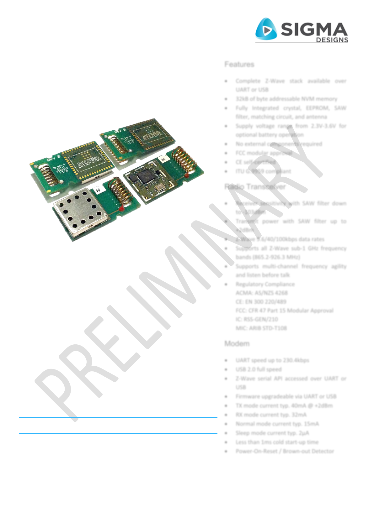
The Sigma Designs ZM5304 Modem is a fully integrated Z-Wave modem
module in a small 27mmx15.2mmx5.5mm form factor. It is an ideal
solution for home control applications such as access control, appliance
control, AV control, building automation, energy management, lighting,
security, and sensor networks in the “Internet of Things”.
A baseband controller, sub-1 GHz radio transceiver, crystal, decoupling,
SAW filter, matching, and the antenna is included to provide a complete
Z-Wave solution to an application executing in an external host
microcontroller. The ZM5304 Modem is certified with the FCC modular
approval, ready to be used in any product without additional testing and
license costs.
The ZM5304 Modem is based on an 8-bit 8051 CPU core, which is
optimized to handle the data and link management requirements of a
Z-Wave node. The UART or USB interface can be used to access the
Z-Wave stack available in the on-chip Flash memory, or to easily upgrade
the modem firmware.
UART or USB
32kB of byte addressable NVM memory
filter, matching circuit, and antenna
optional battery operation
No external components required
FCC modular approval
CE self-certified
ITU G.9959 compliant
Radio Transceiver
to -103dBm
+2dBm
Z-Wave 9.6/40/100kbps data rates
bands (865.2-926.3 MHz)
and listen before talk
Regulatory Compliance
ACMA: AS/NZS 4268
CE: EN 300 220/489
FCC: CFR 47 Part 15 Modular Approval
IC: RSS-GEN/210
MIC: ARIB STD-T108
Modem
UART speed up to 230.4kbps
USB 2.0 full speed
USB
Firmware upgradeable via UART or USB
TX mode current typ. 40mA @ +2dBm
RX mode current typ. 32mA
Normal mode current typ. 15mA
Sleep mode current typ. 2µA
Less than 1ms cold start-up time
Power-On-Reset / Brown-out Detector
DSH12461-3 | 7/2013 1

Datasheet: ZM5304
1 CONTENT
2 OVERVIEW .......................................................................................................................................................................... 4
2.1 PERIPHERALS ........................................................................................................................................................................... 4
2.1.1 Advanced Encryption Standard Security Processor ..................................................................................................... 4
2.1.2 Analog-to-Digital Converter ........................................................................................................................................ 5
2.1.3 Crystal Driver and System Clock .................................................................................................................................. 5
2.1.4 Interrupt Controller ..................................................................................................................................................... 5
2.1.5 Power-On-Reset / Brown-Out Detector ....................................................................................................................... 6
2.1.6 Reset Controller ........................................................................................................................................................... 6
2.1.7 Universal Asynchronous Receiver / Transmitter ......................................................................................................... 6
2.1.8 Universal Serial Bus ..................................................................................................................................................... 6
2.1.9 Watchdog .................................................................................................................................................................... 7
2.1.10 Wireless Transceiver.................................................................................................................................................... 7
2.2 MEMORY MAP ........................................................................................................................................................................ 7
2.3 MODULE PROGRAMMING .......................................................................................................................................................... 8
2.3.1 Entering In-System Programming Mode ..................................................................................................................... 8
2.3.2 Entering Auto Programming Mode ............................................................................................................................. 8
2.4 POWER SUPPLY REGULATOR ...................................................................................................................................................... 8
3 TYPICAL APPLICATION ........................................................................................................................................................ 9
4 PAD CONFIGURATION ....................................................................................................................................................... 10
4.1 PAD FUNCTIONALITY ............................................................................................................................................................... 10
5 ELECTRICAL CHARACTERISTICS .......................................................................................................................................... 12
5.1 TEST CONDITIONS .................................................................................................................................................................. 12
5.1.1 Typical Values ............................................................................................................................................................ 12
5.1.2 Minimum and Maximum Values ............................................................................................................................... 12
5.2 ABSOLUTE MAXIMUM RATINGS ................................................................................................................................................ 13
5.3 GENERAL OPERATING RATINGS ................................................................................................................................................. 13
5.4 CURRENT CONSUMPTION ........................................................................................................................................................ 13
5.5 SYSTEM TIMING ..................................................................................................................................................................... 14
5.6 NON-VOLATILE MEMORY RELIABILITY ........................................................................................................................................ 15
5.7 ANALOG-TO-DIGITAL CONVERTER ............................................................................................................................................. 16
5.8 DC CHARACTERISTICS ............................................................................................................................................................. 16
5.9 RF CHARACTERISTICS .............................................................................................................................................................. 17
5.9.1 Transmitter................................................................................................................................................................ 17
5.9.2 Receiver ..................................................................................................................................................................... 18
5.9.3 Antenna ..................................................................................................................................................................... 21
5.9.4 Regulatory Compliance ............................................................................................................................................. 22
6 Z-WAVE FREQUENCIES ...................................................................................................................................................... 23
7 MODULE INFORMATION ................................................................................................................................................... 24
7.1 MODULE MARKING ................................................................................................................................................................ 24
7.2 MODULE DIMENSIONS ............................................................................................................................................................ 24
8 PCB MOUNTING AND SOLDERING..................................................................................................................................... 25
8.1 RECOMMENDED PCB MOUNTING PATTERN ................................................................................................................................ 25
8.2 RECOMMENDED PLACEMENT ON PCB ....................................................................................................................................... 26
2 DSH12461-3 | 7/2013

Datasheet: ZM5304
8.3 SOLDERING INFORMATION ....................................................................................................................................................... 26
9 ORDERING INFORMATION ................................................................................................................................................ 28
9.1 TAPE AND REEL INFORMATION ................................................................................................................................................. 29
10 REVISION HISTORY ........................................................................................................................................................ 31
11 REFERENCES .................................................................................................................................................................. 32
DSH12461-3 | 7/2013 3
Datasheet: ZM5304
EEPROM
Memory
ZM5304
TXD
USB_DP
RESET_N
USB_DM
RXD
VDD
SPI
Voltage
Regulator
UART
USB
Sub-1 GHz
Radio
Transceiver
SD3503
SAW Filter &
Matching
Helical
Antenna
32MHz
XTAL
8051 CPU
Decoupling
Flash
Memory
AES
ADC
POR / BOD
HOST
Application
UART / USB
ZM5304
Z-Wave® Serial API
Z-Wave® Protocol Stack
Network Layer
MAC Layer
PHY Layer
ITU G.9959
2 OVE R VI EW
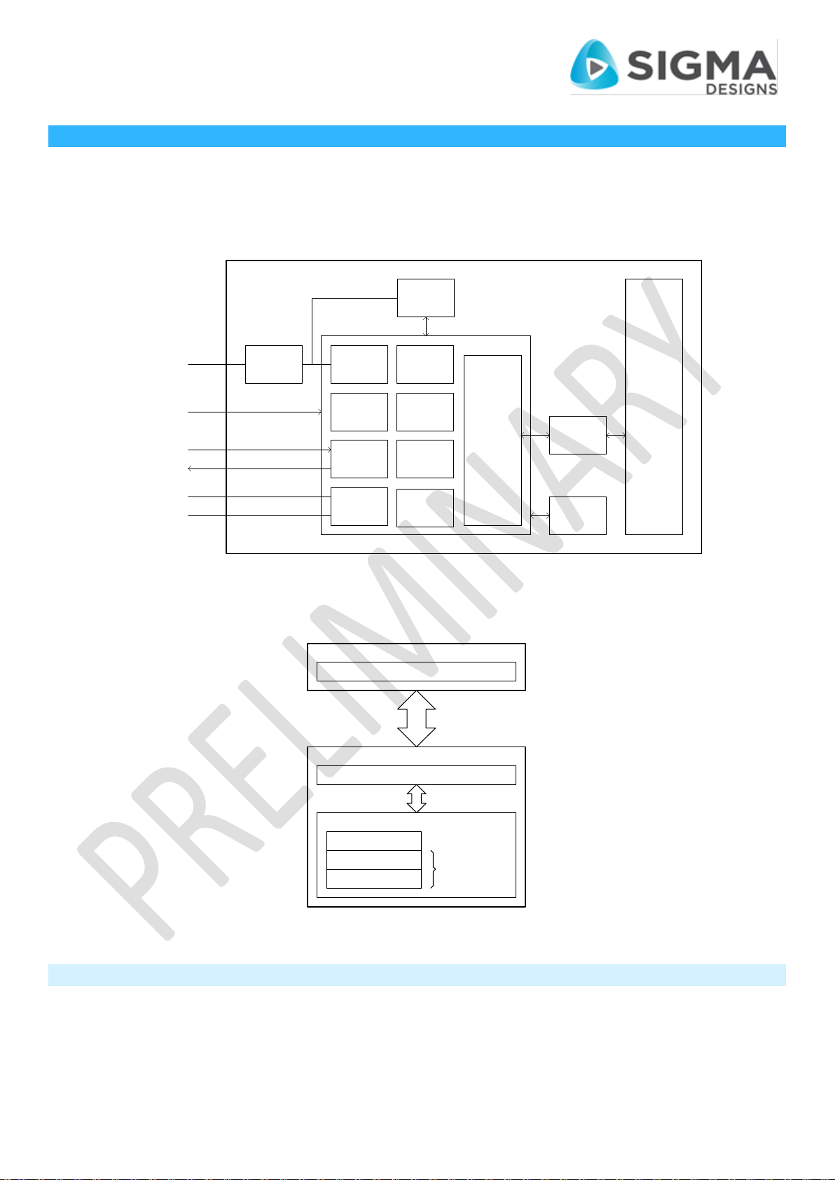
The ZM5304 Modem is a fully integrated module with an on-board antenna that allows the establishment of a Z-Wave network
with minimum risk. The SD3503 modem chip is used with an external NVM (EEPROM), 32MHz crystal, power supply decoupling,
SAW filter, matching circuit, and a helical antenna. Figure 2.1 shows the main blocks of the ZM5304 Modem, while Figure 2.2
illustrates the firmware stack of an example application.
2.1 PERIPHERALS
Figure 2.1: Functional block diagram
Figure 2.2: Firmware stack
2.1.1 ADVANCE D ENCRYPTION STANDARD SE CURITY PROCESSOR
The Z-Wave protocol specifies the use of Advanced Encryption Standard (AES) 128-bit block encryption for secure applications.
The built-in Security Processor is a hardware accelerator that encrypts and decrypts data at a rate of 1 byte per 1.5µs. It encodes
4 DSH12461-3 | 7/2013

Datasheet: ZM5304
Source
Description
Pin
VIN
The sampling input voltage
VBG
V
REF+
The positive node of the reference voltage
VBG, VDD
V
REF-
The negative node of the reference voltage
GND
Vector
Interrupt Name
Priority
Resources served
4
UART
5
UART
7
General Purpose Timer
8
General Purpose Timer
8
ADC 9 Battery monitor, ADC low and high monitor
9
RF
10
RF DMA
14
NMI 0 Non Maskable Interrupt for debugger and more
the frame payload and the message authentication code to ensure privacy and authenticity of messages. The processor supports
Output FeedBack (OFB), Cipher-Block Chaining (CBC), and Electronic CodeBook (ECB) modes to target variable length messages.
Payload data is streamed in OFB mode, and authentication data is processed in CBC mode as required by the Z-Wave protocol.
The processor implements two efficient access methods: Direct Memory Access (DMA) and streaming through Special Function
Register (SFR) ports. The processor functionality is exposed via the Z-Wave API for application use.
2.1.2 ANALO G -TO-DIGITAL CONVERTER
The Analog-to-Digital Converter (ADC) is capable of sampling an input voltage source and returns an 8 or 12 bit unsigned
representation of the input scaled relative to the selected reference voltage, as described by the formula below.
The ADC is capable of operating rail to rail, while the following input configurations apply (VBG = built-in Band-gap 1.25V,
VDD = supply voltage):
Table 2.1: ADC voltage source configuration options
If the sampling input voltage crosses a predefined lower or upper voltage threshold, an interrupt is triggered. Setting VIN = VBG
and V
= VDD implements a battery monitor.
RFE+
2.1.3 CRYSTAL DRIVER AND SYSTEM CL OCK
The system clock and RF frequencies are derived from an external 32MHz crystal (XTAL) which is factory trimmed to guarantee
initial frequency precision. The temperature and 5 years aging margin for the 32MHz crystal is 15 ppm.
2.1.4 INT ERRUPT CONTROLLER
The interrupts are shared between the user application and the Z-Wave protocol. Priorities for the interrupts are pre-assigned
by the Z-Wave protocol implementation. Therefore, constraints for the user application apply.
Table 2.2: Interrupt vector table
DSH12461-3 | 7/2013 5

Datasheet: ZM5304
Reset Cause
Description
GPIO state
Maskable
POR
Reset request generated by Power-OnReset hardware
High impedance with
pull-up
NO
BOR
Reset request generated by Brown-OutReset hardware
High impedance with
pull-up
NO
RESET_N
Reset request generated by the RESET_N
pin being de-asserted
High impedance with
pull-up
NO
WATCHDOG
Reset request generated by the
WATCHDOG Timer timing out
High impedance with
pull-up
YES
START
BIT
D0 D1 D2 D3 D4 D5 D6 D7
STOP
BIT
2.1.5 POWER-ON-RESET / BROWN-OUT DETE C T OR
When a cold start-up occurs, an internal Power-On-Reset (POR) circuit ensures that code execution does not begin unless the
supply voltage is sufficient. After which, an internal Brown-Out Detector (BOD) circuit guarantees that faulty code execution
does not occur by entering the reset state, if the supply voltage drops below the minimum operating level. These guarantees
apply equally in both the active and sleep modes.
2.1.6 RESET CONTROLLER
After a reset event, the MCU is reinitialized in less than 1ms. This delay is mostly due to the charge time of the internal and
external supply capacitances, and bringing the XTAL clock into a stable oscillation. Multiple events may cause a reset. Therefore,
the actual cause is latched by hardware and may be retrieved via software when the system resumes operation. Some reset
methods deliberately leave the state of GPIO pins unchanged, while other GPIO pins are set to high impedance with an internal
weak pull-up.
Table 2.3: Supported reset methods
2.1.7 UNIVER SAL ASYNCHRONOUS RECEI VE R / TRANSMITTER
The Universal Asynchronous Receiver / Transmitter (UART) is a hardware block operating independently of the 8051 CPU. It
offers full-duplex data exchange, up to 230.4kbps, with an external host microcontroller requiring an industry standard NRZ
asynchronous serial data format. The UART interface is available over EP4 and EP5 (refer section 4). A data byte is shifted as a
start bit, 8 data bits (lsb first), and a stop bit, respectively, with no parity and hardware handshaking. Figure 2.3 shows the
waveform of a single serial byte. The UART is compliant with RS-232 when an external level converter is used.
Figure 2.3: UART waveform
2.1.8 UNIVER SAL SERIAL BUS
A Universal Serial Bus (USB) 2.0 full speed interface is available over EP6 and EP7 (refer section 4). The Communication Device
Class / Abstract Control Mode (CDC/ACM) provides an emulated virtual COM port to a host. This makes it easy to migrate from
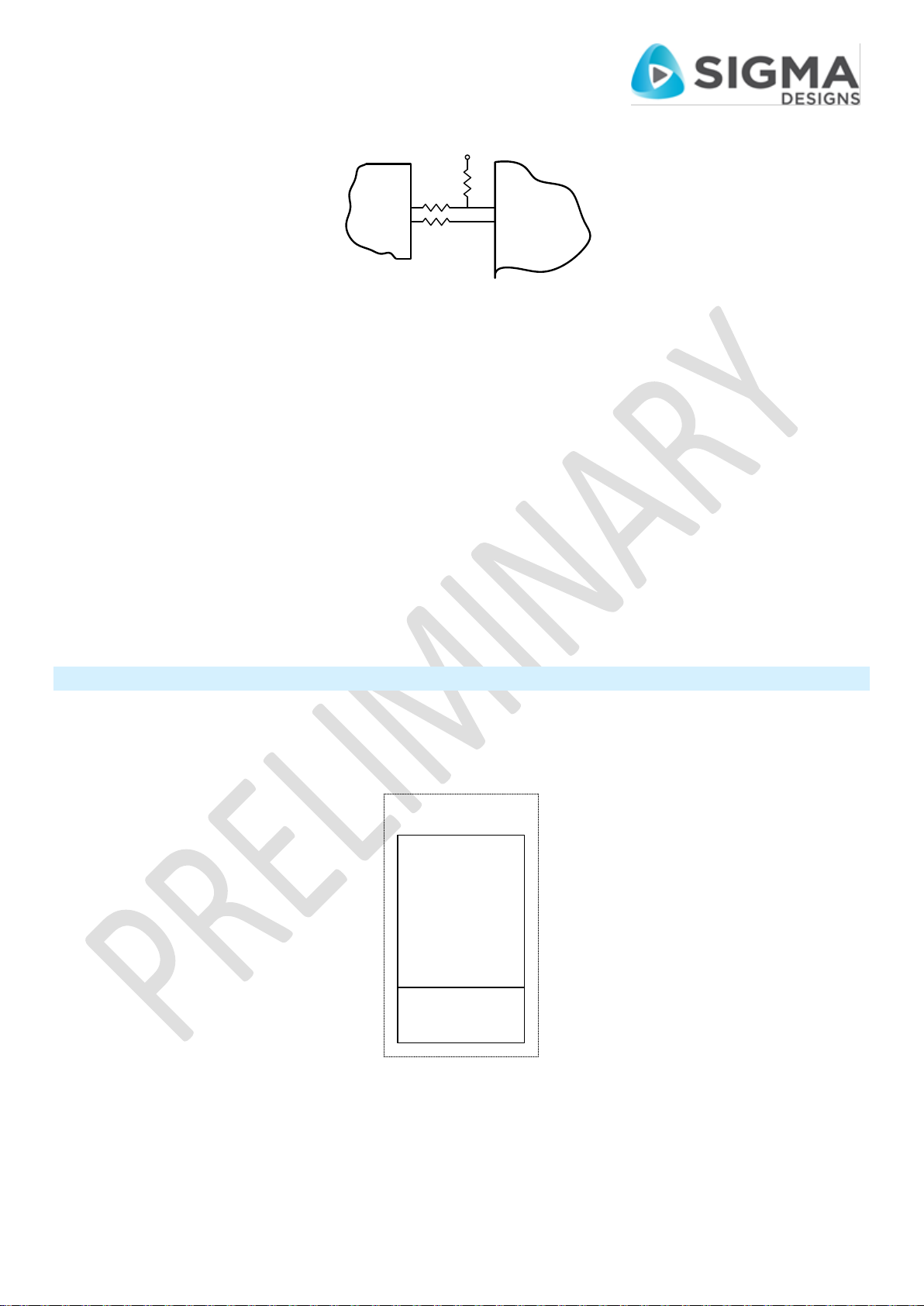
legacy RS-232 communication to USB communication. Figure 2.4 shows the two termination resistors necessary to maintain
signal integrity of the differential pair and a single pull-up resistor on USB_DP, which indicates a full speed device to the host.
6 DSH12461-3 | 7/2013
Datasheet: ZM5304
ZM5304
USB_DP
USB_DM
Host
EEPROM Memory
(Byte addressable)
Protocol Data
(Reserved for Modem)
Application Data
(Available to Host)
0
16kB (min)
Offset
0
Figure 2.4: USB interface
2.1.9 WATCHDOG
The watchdog helps prevents the CPU from entering a deadlock state. A timer that is enabled by default achieves this by
triggering a reset event in case it overflows. The timer overflows in 1 second, therefore it is essential that the software clear the
timer periodically. The watchdog is disabled when the chip is in power down mode, and automatically restarts with a cleared
timer when waking up to the active mode.
2.1.10 WIRELESS TRANSCEIVER
The wireless transceiver is a sub-1 GHz ISM narrowband FSK radio, a modem, and a baseband controller. This architecture
provides an all-digital direct synthesis transmitter and a low IF digital receiver. The Z-Wave protocol currently utilizes 2-key
FSK/GFSK modulation schemes at 9.6/40/100 kbps data rates throughout a span of carrier frequencies from 865.2 to 926.3MHz.
The output power of the transmitter is configurable in the range -26dBm to +2dBm (VDD = 2.3 to 3.6V, TA = -10 to +85°C).
2.2 MEMORY MAP
An application executing on an external host microcontroller can access a minimum of 16kB allocated on the higher address
space of the integrated EEPROM via the serial API. As shown in Figure 2.5, the protocol data is stored in the lower address space.
A serial API function returns the size of the application data space. [1][2]
Figure 2.5: EEPROM memory map
DSH12461-3 | 7/2013 7

Datasheet: ZM5304
2.3 MODULE PROGRAMMING
The firmware of the ZM5304 Modem can be upgraded through the UART or USB interface. [3] In-System Programming is the
default mode delivered from the factory.
2.3.1 ENTERING IN-SYSTEM PROGRAMM ING MODE
The module can be placed into the UART In-System Programming (ISP) mode by asserting the active low RESET_N signal for
4.2ms. The programming unit of the module then waits for the “Interface Enable” serial command before activating the ISP
mode over the UART.
2.3.2 ENTERING AUTO PROGRAMMING M O DE
Alternatively, the module can be placed into the Auto Programming Mode (APM) by calling a serial API function. The
programming unit of the module will enter APM immediately after a hardware or software reset. Once the module is in APM,
the firmware can be written to the internal flash using either the UART or USB interface.
2.4 POWER SUPPLY REGULATOR
While the supply to the digital I/O circuits is unregulated, on-chip low-dropout regulators derive all the 1.5 V and 2.5 V internal
supplies required by the Micro-Controller Unit (MCU) core logic, non-volatile data registers, flash, and the analogue circuitry.
8 DSH12461-3 | 7/2013
Datasheet: ZM5304
ZM5304Host
RESET_N
RXD
TXD
GPIO
TXD
RXD
3V3
3V3
VDD
GND
ZM5304Host
USB_DP
USB_DM
RESET_N
USB_DP
USB_DM
GPIO
3V3
3V3 3V3
1.5kΩ±5%
22Ω±5%
22Ω±5%
VDD
GND
1
3 TYPICAL APPLICATION
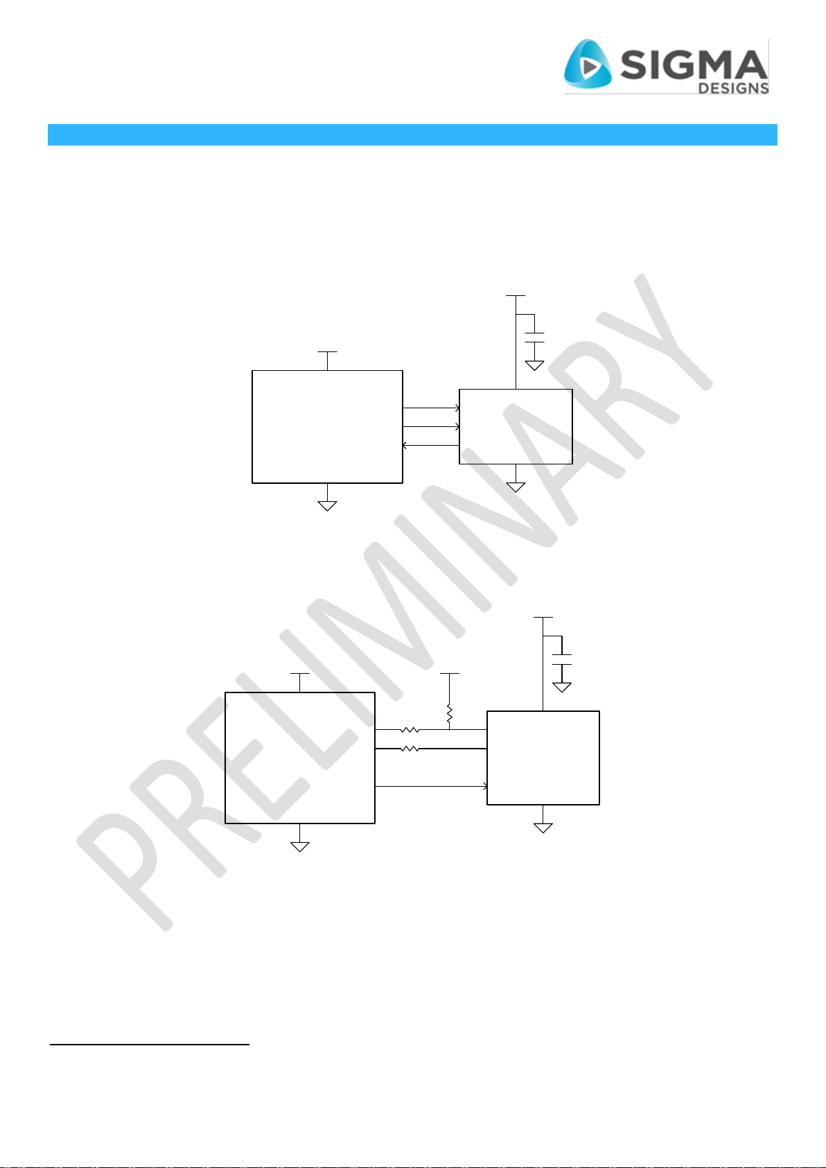
An illustration of two application examples using the ZM5304 Modem implementation follows. The host application located on
an external microcontroller accesses the Z-Wave stack via the serial API. Figure 3.1 depicts the scenario when the UART is used
as the primary interface to the ZM5304 Modem, while Figure 3.2 shows the scenario when the USB1 is used. It is strongly
recommended that the power supply is decoupled sufficiently, and a pull-up resistor placed on the RESET_N signal if the host
GPIO is unable to drive it.
Figure 3.1: Example of a host microcontroller based application using the UART
Figure 3.2: Example of a host microcontroller based application using the USB
Firmware upgrades can be performed only when the ZM5304 Modem is placed in APM.
DSH12461-3 | 7/2013 9
Datasheet: ZM5304
10
9
8
7
6
5
4
3
2
1
48474645444342414039383736
35
11121314151617181920212223
24
B
O
A
R
D
C
U
T
O
U
T
25
26
27
28
29
30
31
32
33
34
GND
VDD
GND
USB_DP
USB_DM
RXD
TXD
NC
RESET_N
GND
GND
GND
GND
GND
NC
NC
NC
NC
GND
NC
GND
GND
NC
NC
NC
NC
NC
NC
NC
NC
NC
NC
NC
NC
NC
NC
NC
NC
NC
NC
NC
NC
NC
NC
NC
NC
GND
Plane
Copper
Free
GND
NC
Pad Name
Pad Location
Type2
Function
VDD 9 S
Module power supply.
GND
1, 8, 10, 11, 24, 25, 28, 30, 34, 35, 48
S
Ground. Must be connected to the ground
plane.
NC
3, 12, 13, 14, 15, 16, 17, 18, 19, 20, 21, 22, 23, 26, 27,
29, 31, 32, 33, 36, 37, 38, 39, 40, 41, 42, 43, 44, 45, 46,
47
-
Placement pads for mechanical stability.
Leave unconnected.
Pad Name
Pad Location
Type
Function
RESET_N 2 I
Active low signal that places the module in
a reset state.
2
4 PAD CONFIGURATION
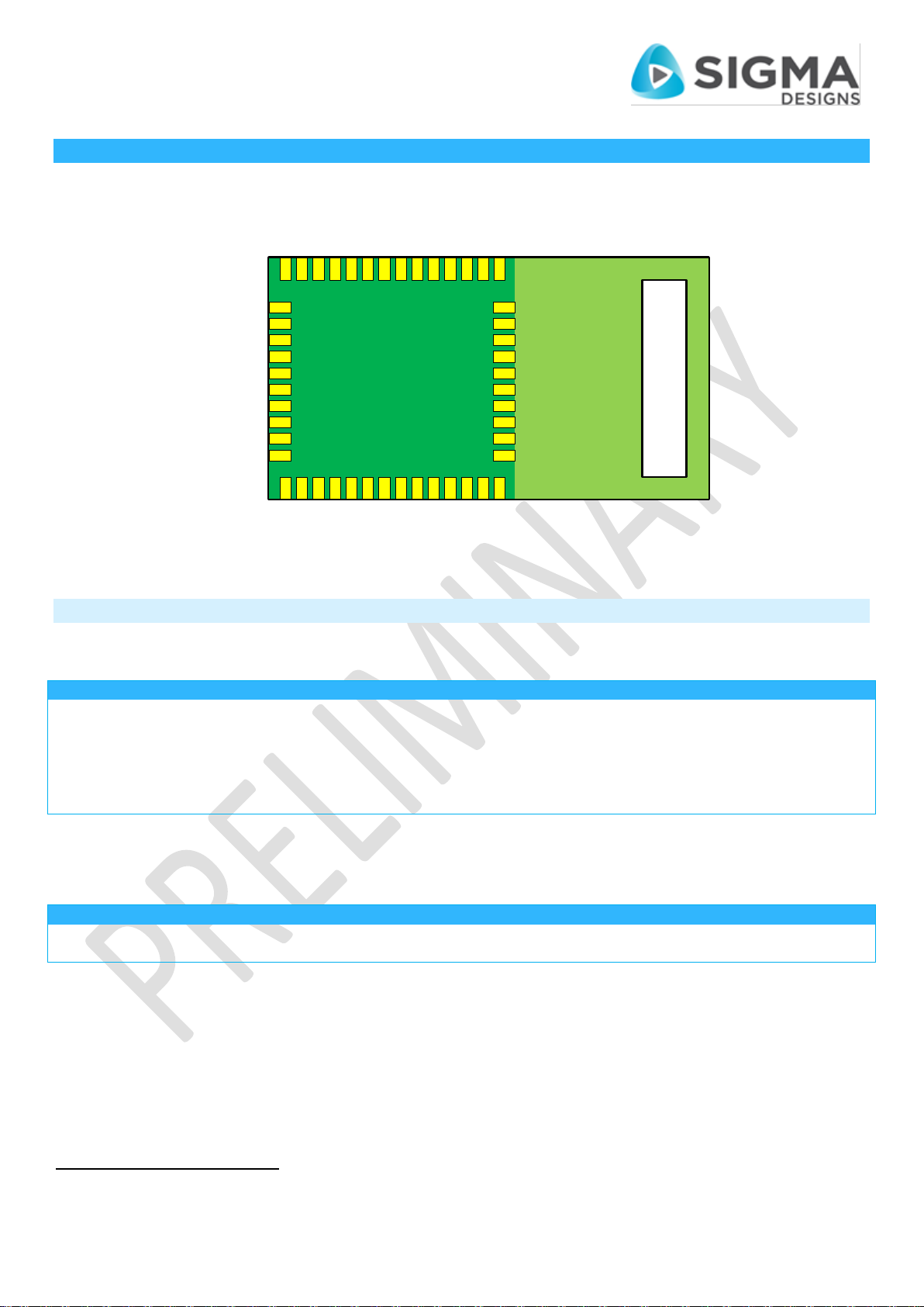
The layout of the Exposed Pads (EP) on the ZM5304 Modem is shown in Figure 4.1.
4.1 PAD FUNCTIONALITY
Figure 4.1: Pad layout (top view)
Table 4.1: Power, ground, and no connect signals
Table 4.2: Module control signals
I = Input, O = Output, D+ = Differential Plus, D- = Differential Minus, S = Supply
10 DSH12461-3 | 7/2013

Datasheet: ZM5304
Pad Name
Pad
Location
Type
Function in Reset State
Function in Active State
RXD 5 I
Waits for the “Interface Enable” serial
command after 4.2ms. Enters ISP mode
after command is received from the host.
Receive data from host serial port.
TXD 4 O
Serial data transmit when in ISP mode,
high impedance otherwise.
Transmit data to host serial port.
Pad Name
Pad
Location
Type
Function in Reset State
Function in Active State
USB_DP
7
D+
USB 2.0 full speed APM when serial API
function is used before entering the reset
state.
USB 2.0 full speed.
USB_DM
6
D-
Table 4.3: UART interface signals
Table 4.4: USB interface signals
DSH12461-3 | 7/2013 11
 Loading...