

SIGE SE2520L Datasheet
SE2520L
RangeCharger™ 2.4GHz Power Amplifier IC
Final
Applications
IEEE 802.11b DSSS Radios, Wireless LAN
2.4GHz Cordless Phones, ISM Radios
Bluetooth™ Wireless Technology
Features
High linear output power for IEEE802.11b,
+20dBm, ACPR 1st lobe –30dBc, 2nd lobe –50dBc
Low current consumption: 110mA at 3.3V
High saturated output power for cordless
telephone applications: +23dBm, 140mA at 3.6V
Single supply voltage: 2.7 to 3.6V
Wide Temperature range: -40 to +85°C
Integrated linear analog control for DC current
and output power management
Small plastic package, 6 Pin LPCC
Ordering Information
Type Package Remark
SE2520L 6 Pin LPCC
SE2520L-R 6 Pin LPCC
SE2520L-EK1 Evaluation Kit Standard
SE2520L-EK3 Evaluation Kit Power Detect,
Notes: (1) JEDEC QFN package.
(1)
Samples
(1)
Shipped in
Tape & Reel
Filter, Rx/Tx
and Diversity
Switches
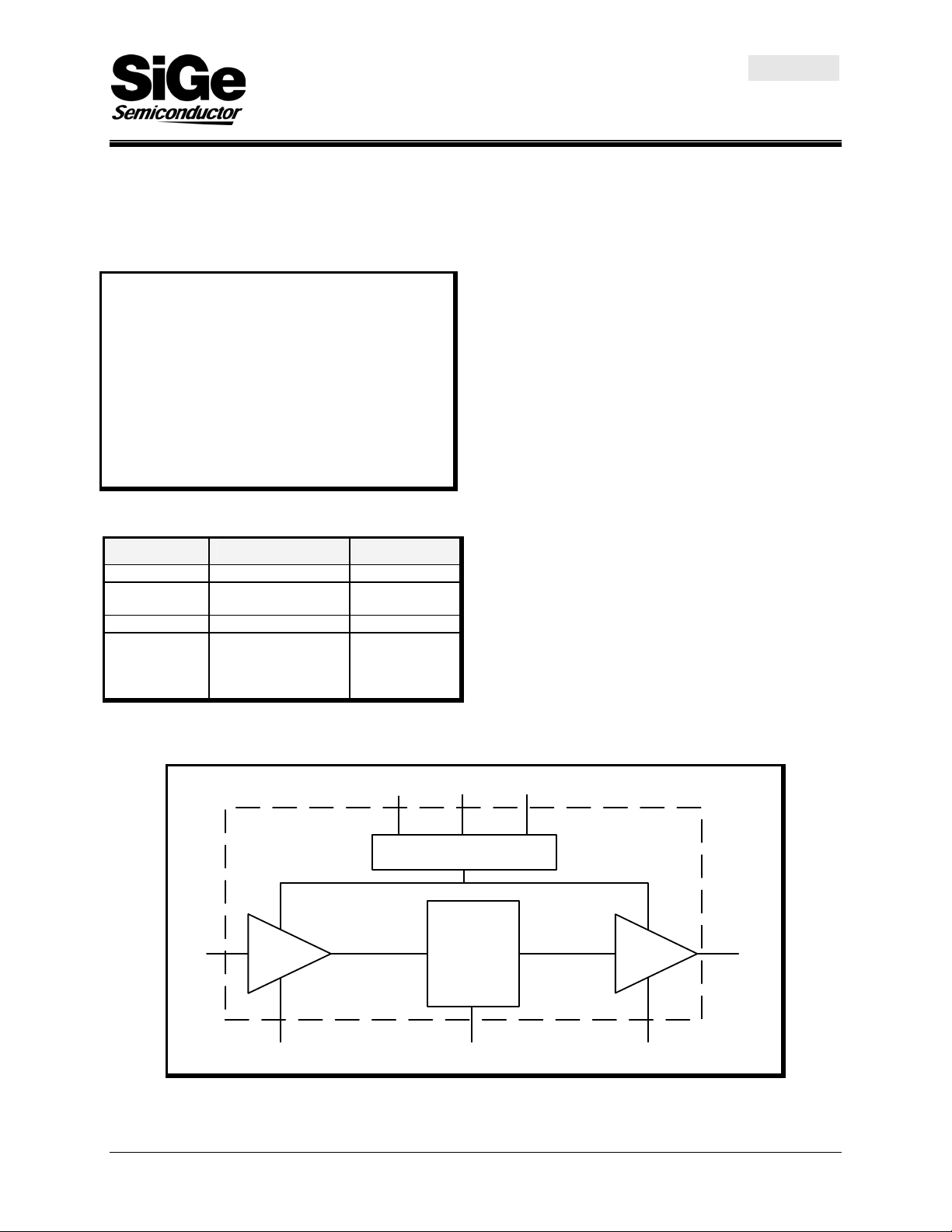
Functional Block Diagram
Product Description
The SE2520L is a power amplifier IC designed for the
2.4GHz ISM band and compliant with the IEEE
802.11b WLAN standard, providing up to +20dBm
typical output power at 3.3V with ACPR of –30dBc 1
lobe and –50dBc 2
For 2.4GHz cordless telephone applications, the
SE2520L produces +23dBm typical saturated output
power at 3.6V.
The SE2520L contains a linear analog control (0.1 to
1.6V) for controlling DC current and output power.
The SE2520L includes a digital enable control for
device on/off control. Ramping is 1 µsec typical.
This device is capable of operating at a duty cycle of
100 percent.
nd
lobe, and requiring only 110mA.
st
V
CTL
V
CC0
V
EN
Bias Generator
IN
Stage 1
GND GND
Interstage
Match
V
CC1
Stage 2
OUT/V
CC2
15-DST-01 Rev 4.8 Oct 28/02 1 of 8
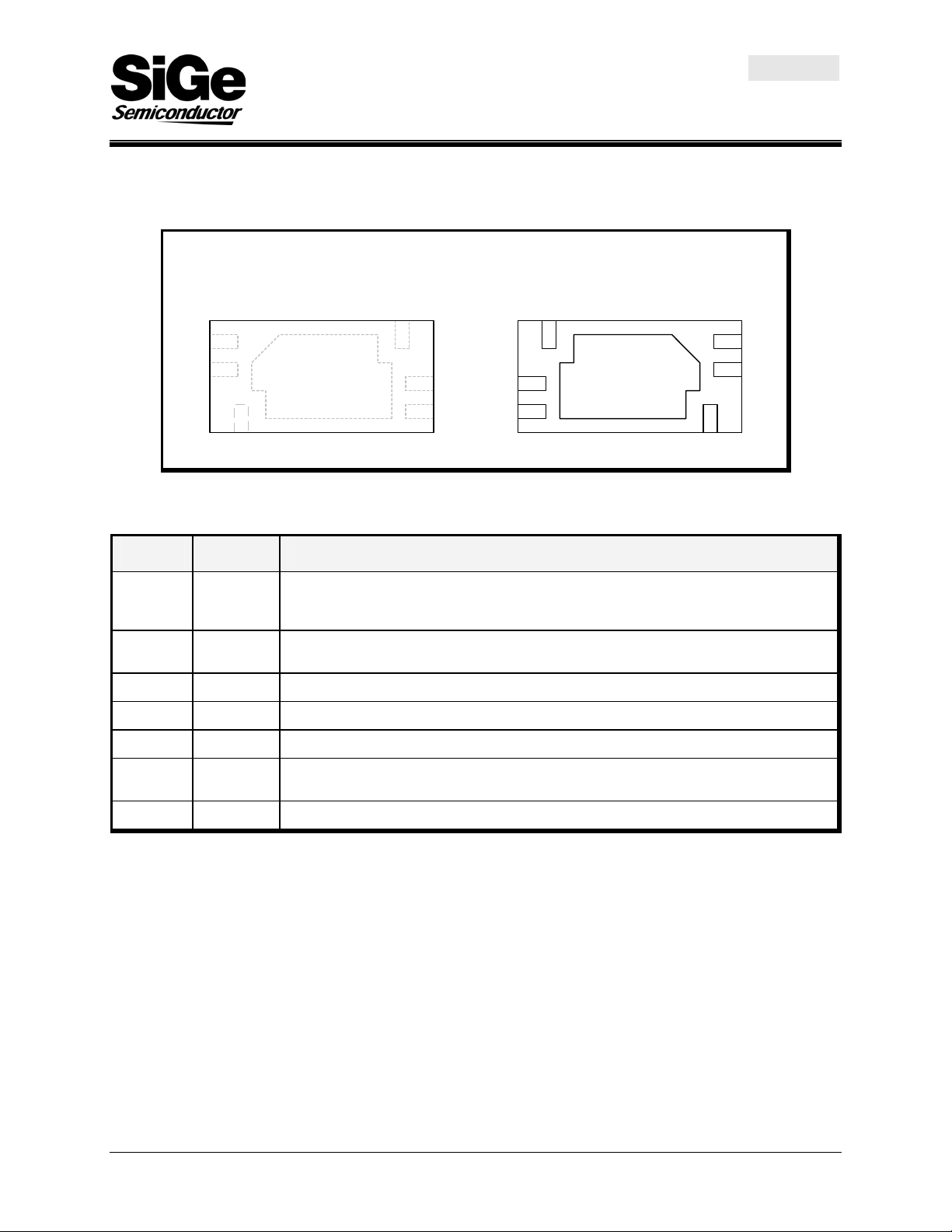
Pin Out Diagram
Note: Pads and die pad shown are at the bottom of package.
SE2520L
RangeCharger™ 2.4GHz Power Amplifier IC
Final
SE2520L
Top View
1
2
2520L
Lot Code
3
6
5
4
5
4
SE2520L
Bottom View
6
Die Pad
1
2
3
Pin Out Description
Pin No. Name Description
Controls the RF output power level and DC current of the power amplifier. An analog
1
2
3 IN Power amplifier RF input, external input matching network with DC blocking is required.
4
5
6
V
CTL
V
EN
V
CC0
V
CC1
OUT/V
control signal between 0.1V and 1.6V varies the PA output power between Min. and
Max. values.
Power Amplifier Enable pin. A digital control signal with logic high (power up) and logic
low (power down) is used to turn the device on and off.
Bias supply voltage.
Stage 1 collector supply voltage, an external inter-stage matching network is required.
PA Output and Stage2 collector supply voltage, external output matching network with
CC2
DC blocking is required.
Die Pad GND Heatslug Die Pad is ground
15-DST-01 Rev 4.8 Oct 28/02 2 of 8
SE2520L
RangeCharger™ 2.4GHz Power Amplifier IC
Final
Absolute Maximum Ratings
These are stress ratings only. Exposure to stresses beyond these maximum ratings may cause permanent damage
to, or affect the reliability of the device. Avoid operating the device outside the recommended operating conditions
defined below. This device is ESD sensitive with an ESD rating of < 600V. Handling and assembly of this device
should be at ESD protected workstations.
Symbol Parameter Min. Max. Unit
VCC Supply Voltage (V
V
Control Voltage -0.3 V
CTL
CC0
, V
CC1
, V
) -0.3 +3.6 V
CC2
V
CC
VEN Power Amplifier Enable -0.3 VCC V
IN RF Input Power +8 dBm
T
Storage Temperature Range -40 +150
STG
Tj Maximum Junction Temperature +150
Recommended Operating Conditions
Symbol Parameter Min. Typ. Max. Unit
TA Operating Temperature -40 +85
VCC Supply Voltage 2.7 3.3 3.6 V
DC Electrical Characteristics
Conditions: V
Symbol Parameter Min. Typ. Max. Unit
CC0
= V
CC1
= V
= VEN = 3.3V, V
CC2
SE2520L-EV1 Evaluation Board.
= 1.6V, PIN = -8dBm, T
CTL
= 25°C, f = 2.45GHz, using SiGe
A
°C
°C
°C
ICC Supply Current, V
I
Supply Current (sat) @ PIN = 2dBm 140 175 mA
CC(sat)
= 1.6V, PIN = -8dBm 110 130 mA
CTL
Supply Current variation over temperature from
= 25°C
T
∆Icc
V
I
TEMP
CTL
CTL
A
(-40°C < T
< +85°C)
A
PA Output Power Control Voltage Range 0.1 1.6 V
Current Sunk by V
Pin 60 100
CTL
25 %
µA
Logic High Voltage 2.0 V
VEN
Logic Low Voltage 0.8 V
I
Leakage Current when VEN = 0V, V
STBY
= 0V 0.1 200
CTL
µA
15-DST-01 Rev 4.8 Oct 28/02 3 of 8
 Loading...