SIGE SE1230Q Datasheet

2
A
LightCharger™ 2.5 Gb/s Automatic Gain Control Amplifier
Applications
SONET/SDH-based transmission systems, test
equipment and modules
OC-48 fibre optic modules
Gigabit Ethernet
Fibre Channel
Wideband RF gain block
Features
Single +3.3 V supply
Power dissipation = 230 mW (typ)
Noise figure < 12 dB
Small signal gain = 23.5 dB differential
Fully integrated AGC function
On-chip 50 Ω input and output terminations
Wide bandwidth (–3 dB) > 2.0 GHz
Maximum input level of 200 mVpk
AGC output level of 370 mVpk differential
Loss of signal functionality
Single-ended or differential operation
Minimal external components
Operating ambient temperature range = -40°C to
+85°C
Equivalent to Nortel Networks AC10
Ordering Information
SE1230Q
Final
Product Description
SiGe Semiconductor offers a portfolio of optical
networking ICs for use in high-performance optical
transmitter and receiver functions, from 155 Mb/s up
to 12.5 Gb/s.
SiGe Semiconductor’s SE1230 is a fully integrated
AGC amplifier aimed primarily at SONET OC-48 and
SDH STM-16 systems. The device may also be used
in any datacom application with input data rates up to
2.5 Gb/s.
The device is designed with differential I/Os and
signal levels compatible with SiGe Semiconductor’s
SE1030 and SE1031 transimpedance amplifiers. A
system block diagram is shown after the functional
description, on page 4.
Optimum performance is provided by differential
connections but with appropriate terminations, the
device can also be used in single-ended mode if
required by the application.
Type Package Remark
SE1230Q 5 mm, 32 pin LQFP None
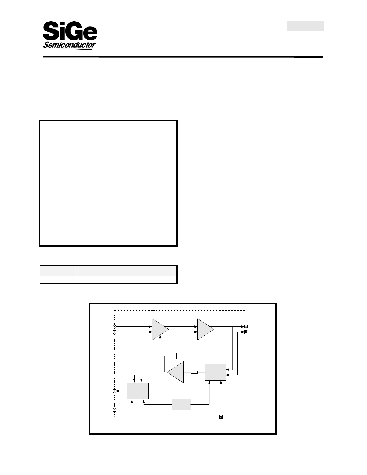
Functional Block Diagram
INP
INN
LOS
LOS_INIT
SE1230
AGC Amp
2.5 Gb/s
Recti fie r/
Comparator
Variable
OUTN OUTP
Gain
Vref
OUTP
Outp ut
Integr ator
Bandgap
Ref
Buffer
Recti fi er
Vref1
GC_ADJ
OUTN
49-DST-01 Rev 1.4 Apr 29/02 1 of 9

A
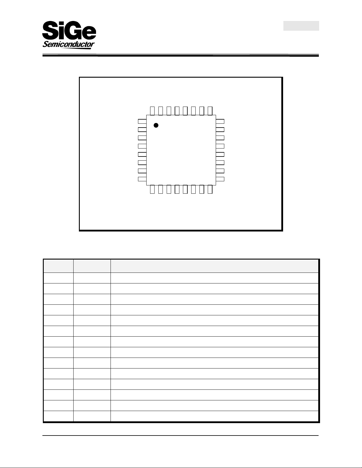
Pin Out Diagram
SE1230Q
LightCharger™ 2.5 Gb/s Automatic Gain Control Amplifier
Final
Pin Out Description
GND
GND
INP
GND
INN
GND
VCC
VCC
VCC
VCC
323130
1
2
3
4
5
6
7
8
9 10 11 12 13 14 15
GND
GND
DNC
DNC DNC
2928272625
Top
View
LOS
VCC
VCC
GC_ADJ
LOS_INIT
VCC VCC
24
23
22
21
20
19
18
17
16
16
GND
GND
GND
GND
OUTP
GND
OUTN
GND
VCC
VCC
Pin No. Name Description
1 GND Negative supply (0 V)
2 GND Negative supply (0 V)
3 INP
4 GND Negative supply (0 V)
5 INN
6 GND Negative supply (0 V)
7 VCC Positive supply (3.3 V)
8 VCC Positive supply (3.3 V)
9 GND Negative supply (0 V)
10 GND Negative supply (0 V)
11 LOS Loss of signal output (open collector)
12 VCC Positive supply (3.3 V)
13 VCC Positive supply (3.3 V)
14 LOS_INIT Sets initial state of LOS output
Non-inverting input (50 Ω impedance)
Inverting input (50 Ω impedance)
49-DST-01 Rev 1.4 Apr 29/02 2 of 9

LightCharger™ 2.5 Gb/s Automatic Gain Control Amplifier
Pin No. Name Description
15 GND Negative supply (0 V)
16 GND Negative supply (0 V)
17 VCC Positive supply (3.3 V)
18 VCC Positive supply (3.3 V)
19 GND Negative supply (0 V)
SE1230Q
Final
20 OUTN
21 GND Negative supply (0 V)
22 OUTP
23 GND Negative supply (0 V)
24 GND Negative supply (0 V)
25 VCC Positive supply (3.3 V)
26 VCC Positive supply (3.3 V)
27 AGC_ADJ AGC output level adjust
28 DNC Do not connect
29 DNC Do not connect
30 DNC Do not connect
31 VCC Positive supply (3.3 V)
32 VCC Positive supply (3.3 V)
Inverted output (50 Ω impedance)
Non-inverted output (50 Ω impedance)
49-DST-01 Rev 1.4 Apr 29/02 3 of 9
 Loading...