

SIGE PA2423MB Datasheet
2
PA2423MB
2.4 GHz Bluetooth Class 1 Power Amplifier IC
Production Information
Applications
Bluetooth
USB Dongles
Laptops
Access Points
Cordless Piconets
tm
Class 1
Features
+22.7 dBm at 45% Power Added Efficiency
Low current 80mA typical @ Pout=+20 dBm
Temperature stability better than 1dB
Power-control and Power-down modes
Single 3.3 V Supply Operation
Temperature Rating: -40C to +85C
8 lead Exposed Pad MSOP Plastic Package
Ordering Information
Product Description
A monolithic, high-efficiency, silicon-germanium
power amplifier IC, the PA2423MB is designed
for class 1 Bluetooth
applications. It delivers +22.7 dBm output power
with 45% power-added efficiency – making it
capable of overcoming insertion losses of up to
2.7 dB between amplifier output and antenna
input in class 1 Bluetooth
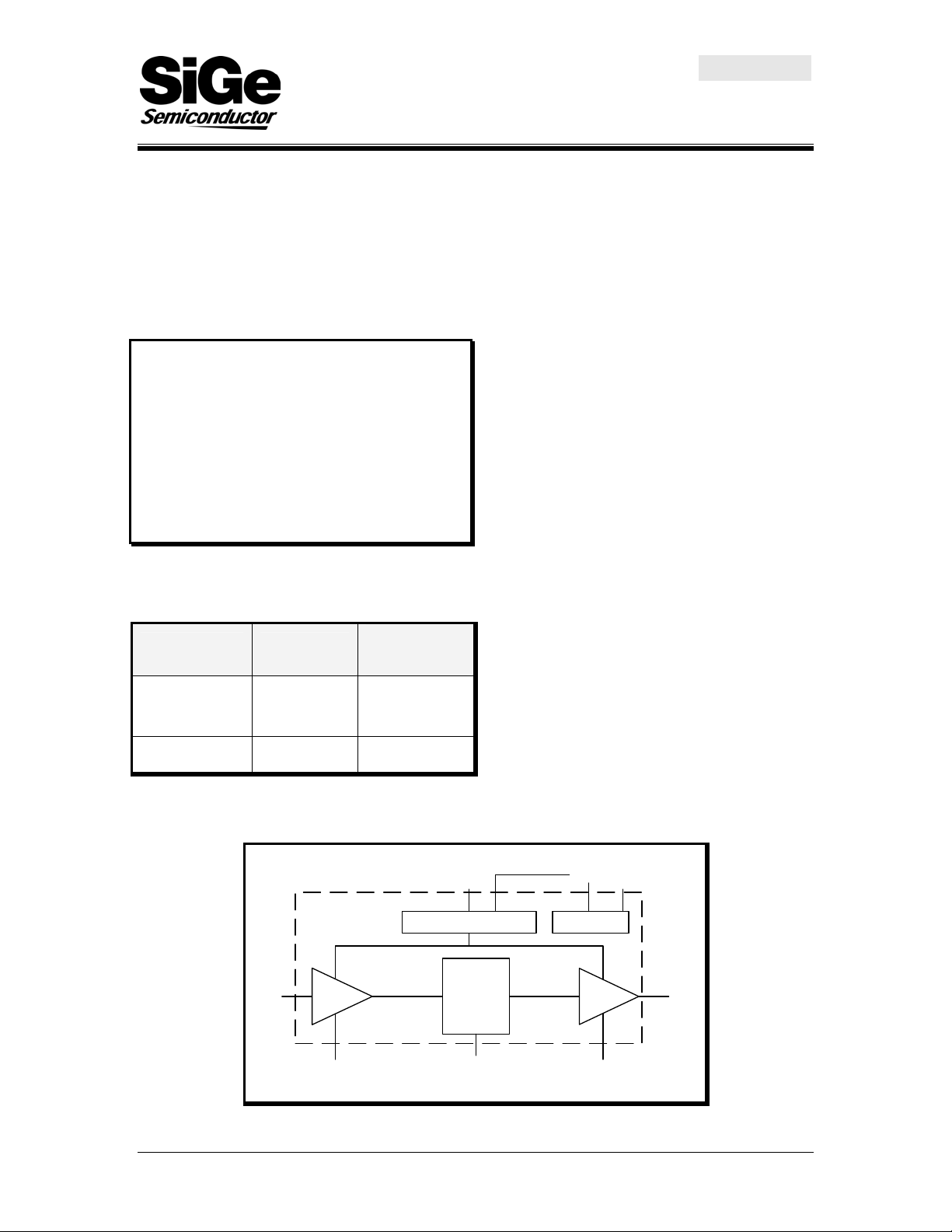
The amplifier features:
an analog control input for improving PAE at
reduced output power levels;
a digital control input for controlling power up
and power down modes of operation.
An on-chip ramping circuit provides the turnon/off switching of amplifier output with less than
3dB overshoot, meeting the Bluetooth
specification 1.1.
The PA2423MB operates at 3.3V DC. At typical
output power level (+22.7 dBm), its current
consumption is 125 mA.
tm
2.4 GHz radio
tm
applications.
tm
Type Package
Shipping
Method
PA2423MB 8 - MSOP Tape and reel
Tubes -samples
PA2423MB-EV Evaluation kit
Functional Block Diagram
Bias Generator
IN
Stage 1
GND GND
V
CTL
Interstage
Match
V
CC1
The silicon/silicon-germanium structure of the
PA2423MB – and its exposed-die-pad package,
soldered to the system PCB – provide high
thermal conductivity and a subsequently low
junction temperature. This device is capable of
operating at a duty cycle of 100 percent.
V
CC0VRAMP
Ramp
Circuitry
Stage 2
OUT/ V
CC
DOC# 05PDS001 Rev 9 07/26/2001 Page 1 of 10
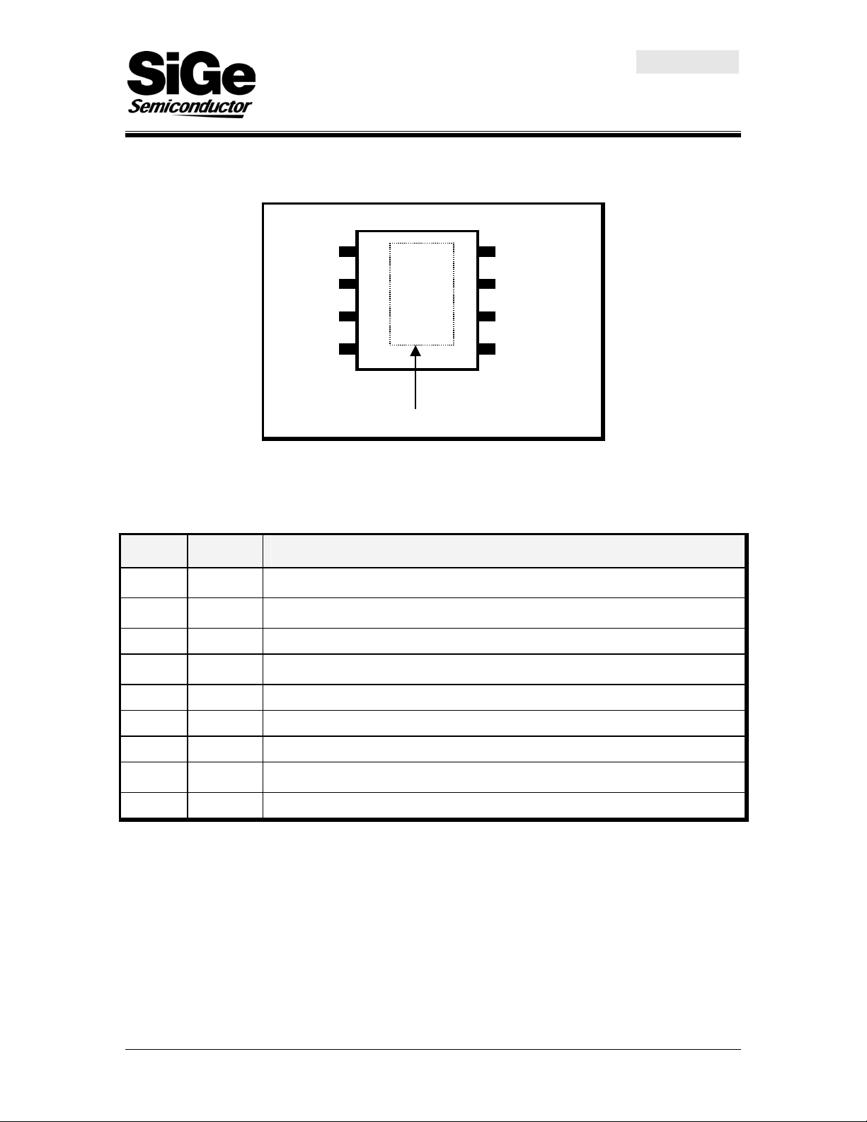
Pin Out Diagram – top view
PA2423MB
2.4 GHz Bluetooth Class 1 Power Amplifier IC
Production Information
VRAMP
VRAMP
VCTL
VCTL
NC
NC
IN
IN
1
Die
Pad
2
3
4 5
Ground
8
7
6
OUT/VCC2
NC
VCC1
VCC1
VCC0
VCC0
Pin Out Description
Pin No. Name Description
1
2
3 NC No connection
4 IN
5
6
7 NC No connection
8
Die Pad GND Heatslug Die Pad is ground
V
CTL
V
RAMP
V
CCO
V
CC1
OUT/V
Controls the output level of the power amplifier. An analog control signal between
0V and Vcc varies the PA output power between minimum and maximum values
Enable/Disable the power amplifier. A digital control signal with Vcc logic high
(power up) and 0V logic low (power down) is used to turn the device on and off.
Power amplifier RF input, external input matching network with DC blocking is
required
Bias supply voltage
Stage 1 collector supply voltage, external inter-stage matching network is required
PA Output and Stage2 collector supply voltage, external output matching network
CC2
with DC blocking is required
DOC# 05PDS001 Rev 9 07/26/2001 Page 2 of 10
PA2423MB
2.4 GHz Bluetooth Class 1 Power Amplifier IC
Production Information
Absolute Maximum Ratings
Symbol Parameter Min. Max. Unit
V
CC
V
CTL
V
RAMP
IN RF Input Power +8 dBm
T
A
T
STG
T
j
Operation in excess of any one of above Absolute Maximum Ratings may result in permanent damage. This
device is a high performance RF integrated circuit with ESD rating < 600V and is ESD sensitive. Handling
and assembly of this device should be at ESD protected workstations.
Supply Voltage -0.3 +3.6 V
Control Voltage -0.3
Ramping Voltage -0.3
Operating Temperature Range
Storage Temperature Range
Maximum Junction Temperature
-40 +85 °C
-40
V
CC
V
CC
+150
+150 °C
V
V
°C
DC Electrical Characteristics
Conditions: VCC0 = VCC1 = VCC2 = VRAMP = 3.3V, VCTL = 3.3V, PIN = +2dBm,TA =25°C, f = 2.45GHz,
Symbol Note Parameter Min. Typ. Max. Unit
∆ICC
Input and Output externally matched to 50Ω ,unless otherwise noted.
VCC
ICC 1 Supply Current (ICC = IVCC0 + IVCC1 +I VCC2), VCTL = 3.3V 125 150 mA
VCTL PA Output Power Control Voltage Range 0 VCC V
ICTL 1 Current sourced by VCTL Pin 200 250
VRAMP
I
stby
3
temp
3 Logic High Voltage 2.0 V
3 Logic Low Voltage
1 Leakage Current when Vramp = 0V, Vctl = high 0.5 10
Supply Voltage 3 3.3 3.6 V
Supply Current variation over temperature from T
(-40°C <TA <+85°C)
= 25°C
A
25 %
0.8 V
µA
µA
DOC# 05PDS001 Rev 9 07/26/2001 Page 3 of 10
 Loading...