

SIGE PA2423G Datasheet
2
PA2423G
2.4 GHz Bluetooth Class 1 Power Amplifier IC
Preliminary Information
Applications
Bluetooth
USB Dongles
Laptops
Access Points
Cordless Piconets
Flip chip and chip-on-board applications
tm
Class 1
Features
+22.5 dBm at 47% Power Added Efficiency
Low current 80 mA typical @ Pout=+20 dBm
Temperature stability better than 1dB
Power-control and Power-down modes
-40C to +85C temperature range
Gold bump bare die (0.63mm x 0.96mm)
Ordering Information
Part Package
PA2423G
Gold bump bare
die
PA2423G-EV Evaluation kit
Shipping
Method
Diced wafer
Waffle pack
Product Description
A monolithic, high-efficiency, silicon-germanium
power amplifier IC, the PA2423G is designed for
Class 1 Bluetoothtm 2.4 GHz radio applications. It
delivers +22.5 dBm output power with 47% poweradded efficiency – making it capable of
overcoming insertion losses of up to 2.5 dB
between amplifier output and antenna input in
Class 1 Bluetooth
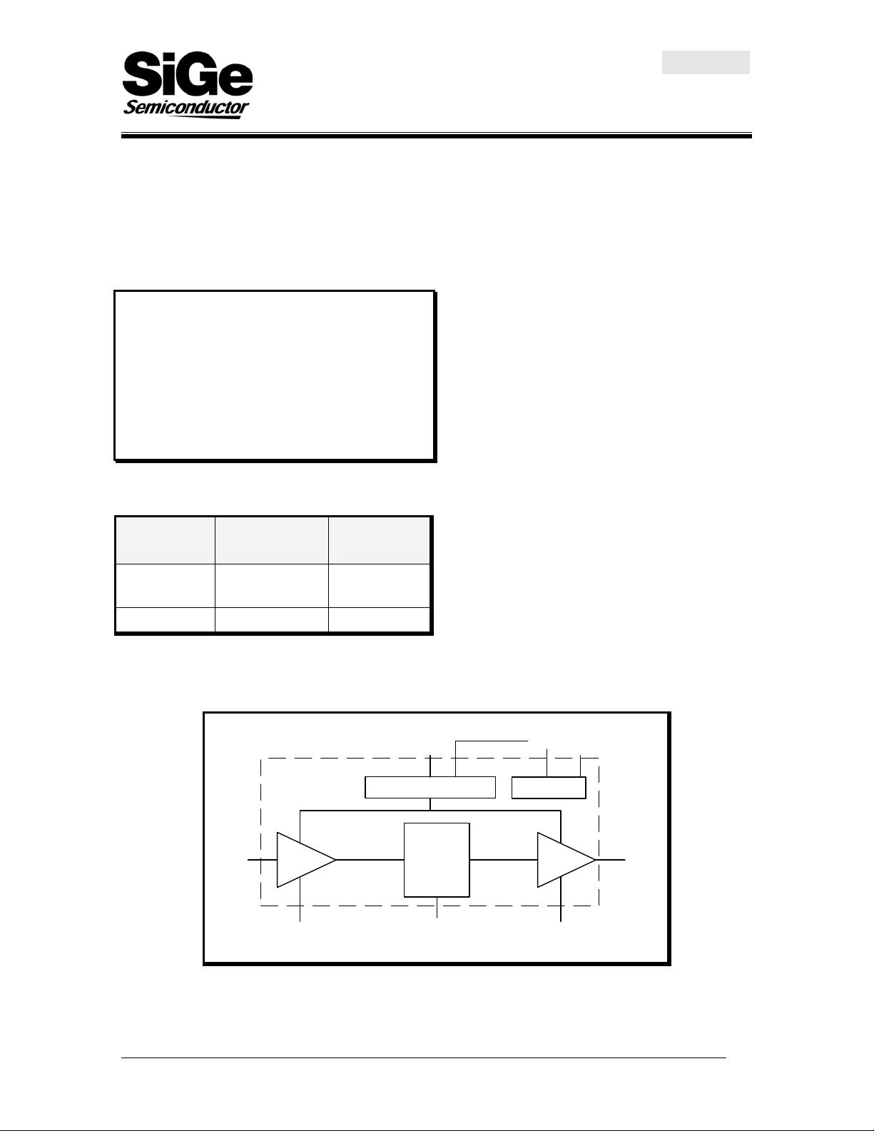
The amplifier features:
an analog control input for improving PAE at
reduced output power levels;
a digital control input for controlling power up
and power down modes of operation.
An on-chip ramping circuit corrects the turn-on/off
switching of amplifier output with less than 3 dB
overshoot, meeting the Bluetooth
The PA2423G operates at 3.3V DC. At typical
output power level (+22.5 dBm), its current
consumption is 120 mA.
The silicon/silicon-germanium structure of the
PA2423G provides high thermal conductivity and
a subsequently low junction temperature. This
device is capable of operating at a duty cycle of
100 percent.
tm
applications.
tm
specification 1.1.
Functional Block Diagram
V
CC0VRAMP
Ramp
Circuitry
Stage 2
OUT/ V
CC
IN
V
CTL
Bias Generator
Stage 1
GND GND
Interstage
Match
V
CC1
DOC # 05PDS003 Rev 5 07/26/2001 Page 1
2.4 GHz Bluetooth Class 1 Power Amplifier IC
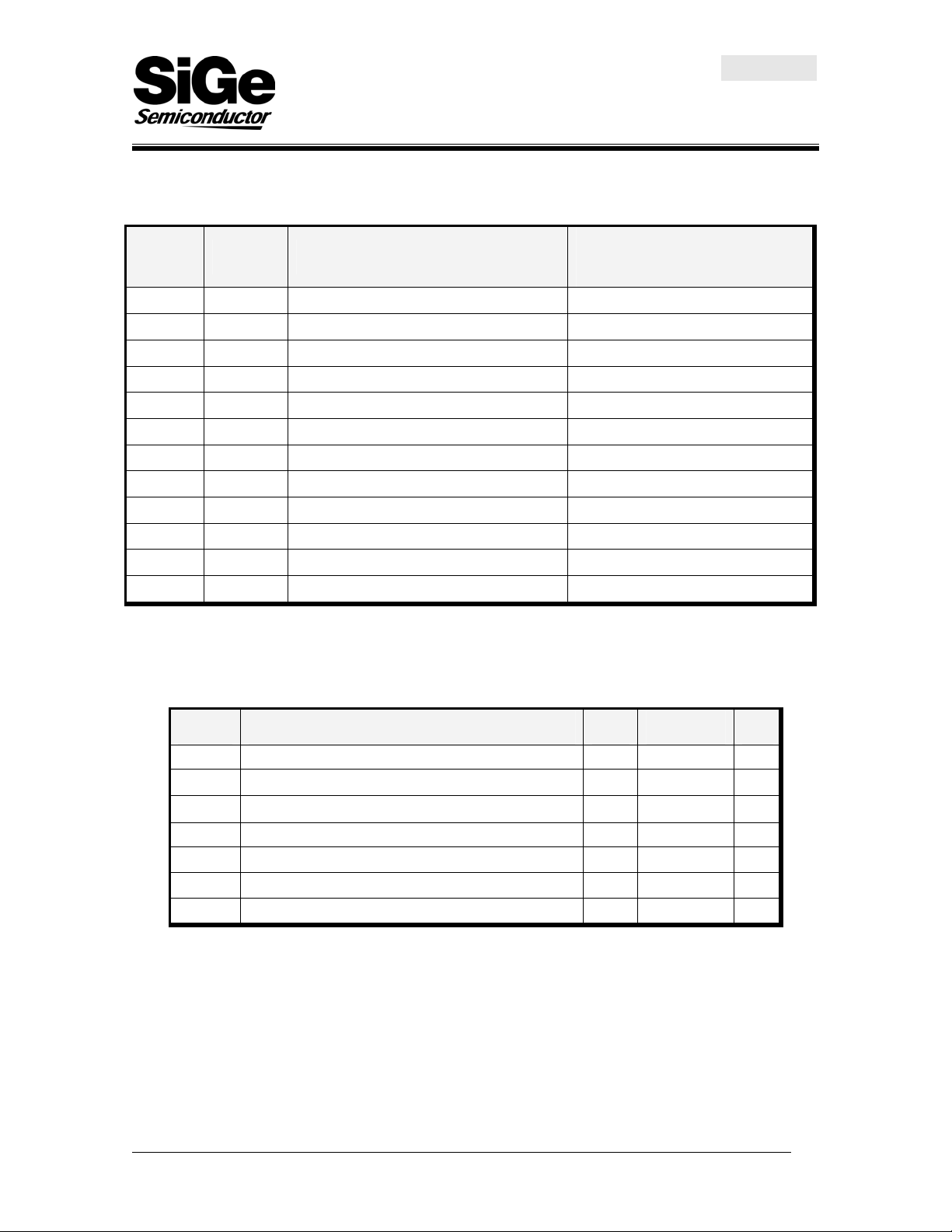
Pad Description
For reference of pad numbers to the package drawings, see pages 4 and 5.
PA2423G
Preliminary Information
Number Name Description
1
2
3
4
5
6
7
8
9
10
11
12
IN PA input X = 192µm ± 10µm, Y = 315µm ± 10µm
VRAMP PA enable/disable control input X = 192µm ± 10µm, Y = 515µm ± 10µm
GND1 Ground X = 352µm ± 10µm, Y = 515µm ± 10µm
VCTL Output power level control X = 512µm ± 10µm, Y = 515µm ± 10µm
GND2 Ground X = 672µm ± 10µm, Y = 515µm ± 10µm
GND3 Ground X = 832µm ± 10µm, Y = 515µm ± 10µm
OUT/VCC2 PA output and stage2 collector supply voltage X = 752µm ± 10µm, Y = 315µm ± 10µm
GND4 Ground X = 832µm ± 10µm, Y = 115µm ± 10µm
GND5 Ground X = 672µm ± 10µm, Y = 115µm ± 10µm
VCC1 Stage1 collector supply voltage X = 512µm ± 10µm, Y = 115µm ± 10µm
GND6 Ground X = 352µm ± 10µm, Y = 115µm ± 10µm
VCC0 Ramp supply voltage X = 192µm ± 10µm, Y = 115µm ± 10µm
Absolute Maximum Ratings
Pad Coordinate, Center of Pad
(lower left corner is (0.0))
Symbol Parameter Min. Max. Unit
VCC Supply Voltage -0.3 +3.6 V
VCTL Control Voltage -0.3
VRAMP Ramping Voltage -0.3
IN RF Input Power +8 dBm
TA Operating Temperature Range
TSTG Storage Temperature Range
Tj Maximum Junction Temperature
Operation in excess of any one of the above Absolute Maximum Ratings may result in permanent damage. This device is a
high performance RF integrated circuit with EST rating < 600V and is ESD sensitive. Handling and assembly of this device
should be at ESD protected workstations.
-40 +85 °C
-40
V
CC
V
CC
+150
+150 °C
V
V
°C
DOC # 05PDS003 Rev 5 07/26/2001 Page 2
DC Electrical Characteristics
PA2423G
2.4 GHz Bluetooth Class 1 Power Amplifier IC
Preliminary Information
Conditions: V
= V
= V
= V
CC0
CC1
CC2
= 3.3V, V
RAMP
= 3.3V, PIN = +2dBm,TA =25°C, f = 2.45GHz,
CTL
Input and Output externally matched to 50Ω ,unless otherwise noted.
Symbol Note Parameter Min. Typ. Max. Unit
VCC
ICC 1 Supply Current (ICC = IVCC0 + IVCC1 + IVCC2 ) 120 150 mA
∆ICC
temp
VCTL PA Output Power Control Voltage Range 0 VCC V
ICTL 1 Current sourced by VCTL Pin 200 250
VRAMP
I
1 Leakage Current when VRAMP = 0V 0.5 10
stby
Supply Voltage 3.0 3.3 3.6 V
3
Supply Current variation over temperature, (-40°C < T
A <+85°C)
25 %
3 Logic High Voltage 2.0 V
3 Logic Low Voltage
0.8 V
AC Electrical Characteristics
Conditions: V
Symbol Note Parameter Min. Typ. Max. Unit
fL-U
POUT
=V
CC0
CC1 =VCC2 =VRAMP
=3.3V, V
CTL
=3.3V,P
=+2 dBm, TA =25°C, f = 2.45GHz,
IN
Input and Output externally matched to 50Ω, unless otherwise noted
Frequency Range
3
240
0
2500 MHz
1 Output Power @ PIN =+2 dBm,VCTL = 3.3V 20.0 22.5 23.5 dBm
1 Output Power @ PIN =+2 dBm,VCTL =0.4V -8 0 dBm
µA
µA
∆P
TEMP
3
P
OUT variation over temperature (-40°C <TA <+85°C), VCTL =3.3V
1 2 dB
dP OUT /dVCTL 3 Control Voltage Sensitivity 60 120 dBm/V
PAE Power Added Efficiency at +22.5 dBm Output Power 47 %
GVAR 3 Gain Variation over band (2400-2500 MHz) 0.7 1 dB
2f, 3f, 4f, 5f 3,4 Harmonics -35 -30 dBc
IS21IOFF 2 Isolation in “OFF” State, PIN =+2dBm,VRAMP =0V 20 25 dB
IS12 I 2 Reverse Isolation 32 42 dB
STAB 2 Stability (PIN = +2dBm, Load VSWR = 6:1)
All non-harmonically related
outputs less than -50 dBc
Notes: (1) Guaranteed by production test at TA =25°C.
(2) Guaranteed by design only.
(3) Guaranteed by design and characterization.
(4) Harmonic levels are greatly affected by topology of external matching networks.
(5) RF characteristics specified above are for direct die attach (Flip-chip) on SiGe Applications
Board. For wire bonded applications there may be some degradation in performance due to
effects of bond wires and interconnect.
DOC # 05PDS003 Rev 5 07/26/2001 Page 3
 Loading...