

SIGE LPT16ED Datasheet
LPT16ED
30 GHz SiGe Bipolar Transistor
Final
Applications
Low phase noise oscillators up to 16 GHz
VCO’s, DRO’s and YIG oscillators
Point-to-point radios
Satellite communications
Fiber optics, OC-192 and OC-768
Local Multipoint Distribution Systems, LMDS
Features
Low 1/f noise: -142 dBc/Hz at 100 Hz offset
Phase noise: -167 dBc/Hz at 100 kHz offset
Output power up to +13 dBm
Operation down to 1 volt, 2 mA
Gold bump pads for wire bond or flip chip (for
direct die attachment)
Ordering Information
Type Package Remark
LPT16ED Bare Die Shipped in
Waffle Pack
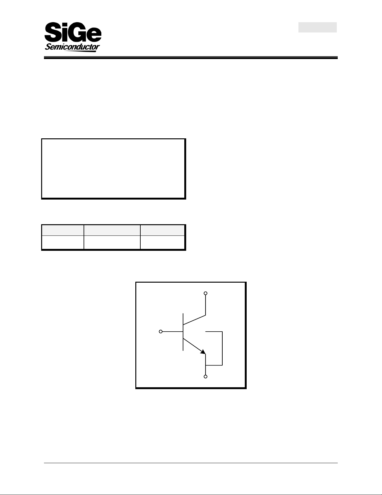
Functional Block Diagram
Product Description
The LPT16ED is a silicon germanium low phase
noise, high frequency NPN transistor for oscillator
applications up to 16GHz.
The transistor exhibits low 1/f noise and provides
+13 dBm typical output power at V
equal to 20 mA. It is easily operated from a single
supply voltage with appropriate external passive
components.
The silicon germanium technology used in this device
provides outstanding high-frequency performance
combined with high thermal conductivity and superior
reliability under harsh operating and storage
conditions.
A complete mechanical description of the transistor is
available under SiGe Semiconductor Document
07MS001.
of 3V and IC
CE
C
B
E
38-DST-01 Rev 2.3 Sept 5/02 1 of 5
LPT16ED
30 GHz SiGe Bipolar Transistor
Final
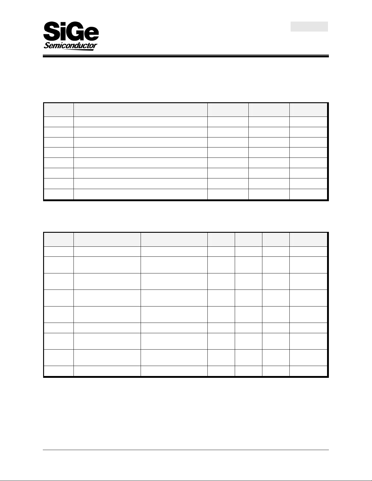
Absolute Maximum Ratings
Operation in excess of any one of Absolute Maximum Ratings may result in permanent damage. This is a high
performance RF device with ESD rating < 2keV. Handling and assembly of this device should be done at ESD
protected workstations.
Symbol Parameter Min. Max. Unit
V
Collector to Base Voltage +13.0 V
CBO
V
Collector to Emitter Voltage +4.0 V
CEO
V
Emitter to Base Voltage +1.5 V
EBO
IC Collector Current 80 mA
IB Base Current 2.0 mA
PT Total Power Dissipation 250 mW
Tj Junction Temperature +150
T
Storage Temperature -65 +150
STG
DC Electrical Characteristics
Conditions: T
Symbol Parameter Condition Min. Typ. Max. Unit
VBE Base-emitter voltage IC = 1µA 670 687 700 mV
BV
CEO
BV
CES
BV
EBO
BV
CBO
VA Early voltage IC = 10mA, VCE = 3V 100 200 300 V
I
CBO
I
EBO
hFE DC current gain VCE = 2V, IC = 20mA 50 60 150
= unless otherwise specified 25°C
A
Collector-emitter
breakdown voltage
Collector-emitter
breakdown voltage
Emitter-base breakdown
voltage
Collector-base
breakdown voltage
Collector-base cutoff
current
Emitter-base cutoff
current
Open base 4.0 4.5 5.0 V
Base-emitter shorted via
100kΩ
= 100µA, open
I
E
collector
14 15.0 16 V
2.0 2.3 2.6 V
Open emitter 14 15.0 16 V
VCB = 5V and IE = 0 100 pA
= 1.5V and IC = 0 5 10 15 µA
V
EB
°C
°C
38-DST-01 Rev 2.3 Sept 5/02 2 of 5
 Loading...